EP3503629A1 - Transceiver device with real time clock - Google Patents
Transceiver device with real time clock Download PDFInfo
- Publication number
- EP3503629A1 EP3503629A1 EP17209427.8A EP17209427A EP3503629A1 EP 3503629 A1 EP3503629 A1 EP 3503629A1 EP 17209427 A EP17209427 A EP 17209427A EP 3503629 A1 EP3503629 A1 EP 3503629A1
- Authority
- EP
- European Patent Office
- Prior art keywords
- clock
- real time
- transceiver device
- wake
- time clock
- Prior art date
- Legal status (The legal status is an assumption and is not a legal conclusion. Google has not performed a legal analysis and makes no representation as to the accuracy of the status listed.)
- Granted
Links
Images

Classifications
-
- H—ELECTRICITY
- H04—ELECTRIC COMMUNICATION TECHNIQUE
- H04W—WIRELESS COMMUNICATION NETWORKS
- H04W56/00—Synchronisation arrangements
- H04W56/001—Synchronization between nodes
- H04W56/0015—Synchronization between nodes one node acting as a reference for the others
-
- H—ELECTRICITY
- H04—ELECTRIC COMMUNICATION TECHNIQUE
- H04L—TRANSMISSION OF DIGITAL INFORMATION, e.g. TELEGRAPHIC COMMUNICATION
- H04L7/00—Arrangements for synchronising receiver with transmitter
- H04L7/0079—Receiver details
- H04L7/0083—Receiver details taking measures against momentary loss of synchronisation, e.g. inhibiting the synchronisation, using idle words or using redundant clocks
-
- H—ELECTRICITY
- H04—ELECTRIC COMMUNICATION TECHNIQUE
- H04L—TRANSMISSION OF DIGITAL INFORMATION, e.g. TELEGRAPHIC COMMUNICATION
- H04L7/00—Arrangements for synchronising receiver with transmitter
- H04L7/04—Speed or phase control by synchronisation signals
- H04L7/08—Speed or phase control by synchronisation signals the synchronisation signals recurring cyclically
-
- H—ELECTRICITY
- H04—ELECTRIC COMMUNICATION TECHNIQUE
- H04W—WIRELESS COMMUNICATION NETWORKS
- H04W52/00—Power management, e.g. Transmission Power Control [TPC] or power classes
- H04W52/02—Power saving arrangements
- H04W52/0209—Power saving arrangements in terminal devices
- H04W52/0212—Power saving arrangements in terminal devices managed by the network, e.g. network or access point is leader and terminal is follower
- H04W52/0216—Power saving arrangements in terminal devices managed by the network, e.g. network or access point is leader and terminal is follower using a pre-established activity schedule, e.g. traffic indication frame
-
- H—ELECTRICITY
- H04—ELECTRIC COMMUNICATION TECHNIQUE
- H04W—WIRELESS COMMUNICATION NETWORKS
- H04W52/00—Power management, e.g. Transmission Power Control [TPC] or power classes
- H04W52/02—Power saving arrangements
- H04W52/0209—Power saving arrangements in terminal devices
- H04W52/0225—Power saving arrangements in terminal devices using monitoring of external events, e.g. the presence of a signal
- H04W52/0229—Power saving arrangements in terminal devices using monitoring of external events, e.g. the presence of a signal where the received signal is a wanted signal
- H04W52/0235—Power saving arrangements in terminal devices using monitoring of external events, e.g. the presence of a signal where the received signal is a wanted signal where the received signal is a power saving command
-
- H—ELECTRICITY
- H04—ELECTRIC COMMUNICATION TECHNIQUE
- H04W—WIRELESS COMMUNICATION NETWORKS
- H04W52/00—Power management, e.g. Transmission Power Control [TPC] or power classes
- H04W52/02—Power saving arrangements
- H04W52/0209—Power saving arrangements in terminal devices
- H04W52/0261—Power saving arrangements in terminal devices managing power supply demand, e.g. depending on battery level
- H04W52/0274—Power saving arrangements in terminal devices managing power supply demand, e.g. depending on battery level by switching on or off the equipment or parts thereof
- H04W52/028—Power saving arrangements in terminal devices managing power supply demand, e.g. depending on battery level by switching on or off the equipment or parts thereof switching on or off only a part of the equipment circuit blocks
-
- H—ELECTRICITY
- H04—ELECTRIC COMMUNICATION TECHNIQUE
- H04W—WIRELESS COMMUNICATION NETWORKS
- H04W84/00—Network topologies
- H04W84/18—Self-organising networks, e.g. ad-hoc networks or sensor networks
-
- Y—GENERAL TAGGING OF NEW TECHNOLOGICAL DEVELOPMENTS; GENERAL TAGGING OF CROSS-SECTIONAL TECHNOLOGIES SPANNING OVER SEVERAL SECTIONS OF THE IPC; TECHNICAL SUBJECTS COVERED BY FORMER USPC CROSS-REFERENCE ART COLLECTIONS [XRACs] AND DIGESTS
- Y02—TECHNOLOGIES OR APPLICATIONS FOR MITIGATION OR ADAPTATION AGAINST CLIMATE CHANGE
- Y02D—CLIMATE CHANGE MITIGATION TECHNOLOGIES IN INFORMATION AND COMMUNICATION TECHNOLOGIES [ICT], I.E. INFORMATION AND COMMUNICATION TECHNOLOGIES AIMING AT THE REDUCTION OF THEIR OWN ENERGY USE
- Y02D30/00—Reducing energy consumption in communication networks
- Y02D30/70—Reducing energy consumption in communication networks in wireless communication networks
Definitions
- the present invention is generally related to the field of sensor networks.
- Sensor nodes typically comprise a transmitter/receiver structure (i.e. a transceiver), a sensor, a sensor interface, an energy source like e.g. a battery and a controller.
- a transmitter/receiver structure i.e. a transceiver
- a sensor i.e. a sensor
- a sensor interface i.e. a sensor interface
- an energy source like e.g. a battery and a controller.
- the sensor and the energy source may be integrated in the sensor node or be external to it.
- an RF transceiver (which is by far the most power-hungry block in a sensor network) should have an extremely low duty cycle (i.e., the ratio of on-time to sleep time), to minimize the average power consumption.
- the average power consumption of the RF transceiver should be lower than 1 ⁇ W in order to sustain for 10 years with a 100mAh small battery.
- the duty cycle need to be reduced to 10 -5 to achieve an average power below 1 ⁇ W, this requires the real-time-counter accuracy to be approximately 10ppm, i.e., an accuracy similar to that of a crystal oscillator (XO).
- the low-power RC-based real-time-counter typically has an accuracy in the order of 10000 ppm.
- the invention relates to a transceiver device comprising a real time clock arranged for providing a clock signal and a receiving section comprising
- the proposed solution indeed allows for receiving in the wake-up receiver a calibration signal on a regular basis, so that network synchronization becomes possible with reduced power consumption and cost.
- the wake-up receiver is arranged for receiving a wake-up signal and for waking up the main receiver upon reception of the wake-up signal.
- the real time clock is arranged for waking up said main receiver.
- the wake-up receiver is arranged for being enabled periodically via the clock signal from the real-time clock.
- the receiving section preferably comprises a real time clock controller arranged to receive the clock timing information from a transceiver device acting as a master and to compare the received clock timing information with timing information of the real time clock to obtain a timing error for adjusting the real time clock of the transceiver device.
- the real time clock controller advantageously comprises a counter to extract the timing information of the real time clock.
- the transceiver device comprises in certain embodiments comparing means to perform the comparing of the received clock timing information and the timing information of the real time clock.
- the real time clock controller further comprises a digital loop filter to filter the timing error.
- the transceiver device further comprises a sensor device.
- the invention in another aspect relates to a device for use as a sensor node in a sensor network comprising a transceiver device as previously described.
- the invention relates to a communication system comprising one or more transceivers as previously described.
- the communication system comprises a further transceiver arranged to act as a master device.
- the invention relates to a method for calibrating a real time clock of a first transceiver device operative as a slave in a network, the method comprising :
- a main receiver forming part of said receiving section of said first transceiver device is woken up with said wake up receiver, once said calibration signal has been received.
- the wake-up receiver is periodically enabled via a clock signal from the real-time clock.
- the present invention discloses a transceiver device with a novel structure as well as a method for calibrating such a transceiver device when it is part of a network.
- FIG.1 A network of wireless nodes is shown.
- One wireless transceiver is used as a master node.
- Two more transceiver devices are shown that act as a slave node.
- each of the slave devices is provided with a real-time clock 20.
- the transceiver devices acting as slave have a receiving section not only comprising a main receiver 40 that can receive communication signals, but also a wake-up receiver 10.
- the invention also unveils a calibration method wherein this wake-up receiver performs a crucial role.
- the wake-up receiver (WuRX) 10 is periodically enabled by the clock signal of the real-time counter (RTC) 20.
- RTC real-time counter
- the terms 'real-time counter' and real-time clock' refer to the same and are used interchangeably.
- the wake-up receiver is ready to receive from the master node a calibration signal containing clock timing information and/or wake-up signal.
- the receiving section also comprises a real time clock controller 30, which receives the clock timing information received from the master device. Based on the received clock timing information the slave device can then correct the clock signal of the real-time counter, as will be detailed below.
- the transmitter in the master node employs a precise crystal oscillator to generate a correct timing reference. It periodically transmits the calibration signal with the timing information, including a time stamp, to the slave devices.
- the precise crystal oscillator in the master node is further also used to generate a stable signal centre frequency.
- the wake-up receiver is continuously enabled. In this way the wake-up is at any time ready to listen to an incoming calibration signal.
- the wake-up receiver wakes up the main receiver in the receiving section of the slave transceiver device once the wake-up signal is received. This reduces the on time of the main receiver.
- the wake-up signal is sent just before the master node transmits a communication signal to the slave node.
- the main receiver is woken up directly via a clock signal from the real-time counter (RTC) 20. This is illustrated with a dashed line in Fig.2 .
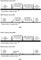
- Fig.3 illustrates a typical communication scheme. At regular times the wake-up receiver in the slave device is enabled. It can then receive the calibration signal that contains the clock timing information. Fig.3 also illustrates a second calibration signal transmission and a third signal - a wake-up signal - transmission. The wake-up signal transmission occurs just before transmitting the main burst signal.
- Fig.4 provides a similar scheme as Fig.3 , but now for the case the wake-up receiver is continuously enabled. The wake-up receiver is then all the time ready for receiving a calibration signal containing clock timing information.
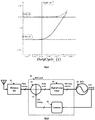
- Fig.5 illustrates the calculated average power consumption (in ⁇ W) versus duty cycle.
- the upper curve is calculated based on a typical real time clock with calibration, whereas the lower curve is calculated based on a real time clock calibrated as proposed in this invention.
- the average power consumption with a real time clock without calibration is limited to around 10 ⁇ W, even the duty cycle is reduced to below 10 -5 .
- the real time clock is being calibrated to an accuracy of 10ppm, it brings down the average power consumption of the slave node to 0.9 ⁇ W when the clock duty cycle is reduced to 10 -5 .
- the wake-up receiver receives via its antenna the calibration signal comprising a time stamp.
- Fig.6 provides a more detailed view on the real time clock controller that receives the clock timing information from the master device.
- the real-time controller is further arranged for comparing this information with timing information derived from the real-time clock comprised in the slave transceiver.
- the controller advantageously comprises a counter to extract real-time information from the real-time clock output of the slave device. The controller then can determine a timing error by comparing the received clock timing information, i.e. the time stamp contained therein, with timing information of the real time clock.
- a digital loop filter is provided to filter the timing error.
- synchronous network there is a master node as the control centre that organizes the communication with one or more slave devices. These slave devices, which typically include sensors, collect the environmental information to send it to the master node.
- the master node periodically sends control information (or a beacon signal) and the slave nodes need to wake up periodically to receive this control information and possibly send back the sensor data to the master node if that is needed.
- control information or a beacon signal
- the slave nodes need to wake up periodically to receive this control information and possibly send back the sensor data to the master node if that is needed.
- the slave nodes can wake up at the correct time because the real-time clock precision is being calibrated.
- wireless communication networks also use a similar master-slave network structure.
- the base-station of a cellular system is equivalent to a master and the cell phones are the slave devices.
- the receivers of the cell phones need to periodically turn on to receive the control information from the base station.
- a similar approach can be adopted to ensure the wake-up timing of the cell phones are precisely calibrated.
- a computer program may be stored/distributed on a suitable medium, such as an optical storage medium or a solid-state medium supplied together with or as part of other hardware, but may also be distributed in other forms, such as via the Internet or other wired or wireless telecommunication systems. Any reference signs in the claims should not be construed as limiting the scope.
Landscapes
- Engineering & Computer Science (AREA)
- Computer Networks & Wireless Communication (AREA)
- Signal Processing (AREA)
- Electric Clocks (AREA)
- Synchronisation In Digital Transmission Systems (AREA)
- Arrangements For Transmission Of Measured Signals (AREA)
Abstract
Description
- The present invention is generally related to the field of sensor networks.
- Most data collected by sensor nodes which for example form a wireless sensor network, changes very slowly. Consequently, in many applications most data needs to be transmitted only once every few minutes or even every few hours.
- Sensor nodes typically comprise a transmitter/receiver structure (i.e. a transceiver), a sensor, a sensor interface, an energy source like e.g. a battery and a controller. The sensor and the energy source may be integrated in the sensor node or be external to it.
- There is a clear tendency towards the use of batteries with an ever increasing lifetime. To meet the tough goal of a 10-year battery life time with a one-time installation or energy harvest operation, an RF transceiver (which is by far the most power-hungry block in a sensor network) should have an extremely low duty cycle (i.e., the ratio of on-time to sleep time), to minimize the average power consumption. For example, the average power consumption of the RF transceiver should be lower than 1µW in order to sustain for 10 years with a 100mAh small battery.
- There are two key limiting factors for reaching a minimum average power consumption and duty cycle: leakage current and the accuracy of the real-time counter. To address the leakage issue, a sophisticated power management and non-volatile memory have been widely explored. However, the real-time-counter accuracy has so far received little attention. If the real-time-counter has a frequency error of 1%, the lowest duty cycle is also limited to approximately 1%, because the transceiver needs to be enabled longer in order not to lose synchronization. For a transceiver with 10mW peak power, the duty cycle need to be reduced to 10-5 to achieve an average power below 1µW, this requires the real-time-counter accuracy to be approximately 10ppm, i.e., an accuracy similar to that of a crystal oscillator (XO). Note the low-power RC-based real-time-counter typically has an accuracy in the order of 10000 ppm.
- Further reducing the duty cycle does not lead to a reduction of the average power either when the settling time of the main crystal oscillator or the system processing overhead becomes a dominant factor.
- In the art the use of a high precision external temperature compensated crystal oscillator has been proposed. Such a temperature-compensated XO may consume as much as 10 µA, i.e. 100 times more than an on-chip relaxation oscillator. An important drawback is that this is a very expensive solution.
- If a crystal oscillator is used to calibrate the real-time-counter, only the frequency offset is calibrated, but not the noise, temperature or supply voltage induced variation.
- Also in case the frequency is synchronized in the network level, only frequency drift is calibrated, but not the noise induced variation.
- Hence, there is a need for a synchronization method which is ultra-low power in order to enable a long operation life time or energy harvesting based operation.
- It is an object of embodiments of the present invention to provide for a transceiver device comprising a mechanism for accurate wake-up timing. Having such a transceiver device available is an important step towards establishing ultra-low power synchronization in a sensor network. It is also an object of the invention to provide for a method for calibrating such a transceiver device.
- The above objective is accomplished by the solution according to the present invention.
- In a first aspect the invention relates to a transceiver device comprising a real time clock arranged for providing a clock signal and a receiving section comprising
- a main receiver arranged for receiving communication signals,
- a wake-up receiver arranged for receiving a calibration signal comprising clock timing information containing a time stamp and for adjusting said real time clock based on said clock timing information.
- The proposed solution indeed allows for receiving in the wake-up receiver a calibration signal on a regular basis, so that network synchronization becomes possible with reduced power consumption and cost.
- In preferred embodiments the wake-up receiver is arranged for receiving a wake-up signal and for waking up the main receiver upon reception of the wake-up signal.
- In other preferred embodiments the real time clock is arranged for waking up said main receiver.
- In other preferred embodiments the wake-up receiver is arranged for being enabled periodically via the clock signal from the real-time clock.
- The receiving section preferably comprises a real time clock controller arranged to receive the clock timing information from a transceiver device acting as a master and to compare the received clock timing information with timing information of the real time clock to obtain a timing error for adjusting the real time clock of the transceiver device. The real time clock controller advantageously comprises a counter to extract the timing information of the real time clock.
- The transceiver device comprises in certain embodiments comparing means to perform the comparing of the received clock timing information and the timing information of the real time clock.
- In one embodiment the real time clock controller further comprises a digital loop filter to filter the timing error.
- Advantageously, the transceiver device further comprises a sensor device.
- In another aspect the invention relates to a device for use as a sensor node in a sensor network comprising a transceiver device as previously described.
- In one aspect the invention relates to a communication system comprising one or more transceivers as previously described.
- In a preferred embodiment the communication system comprises a further transceiver arranged to act as a master device.
- In another aspect the invention relates to a method for calibrating a real time clock of a first transceiver device operative as a slave in a network, the method comprising :
- enabling a wake-up receiver forming part of a receiving section of said first transceiver device,
- receiving in the wake-up receiver a calibration signal comprising clock timing information containing a time stamp and adjusting the real time clock based on the clock timing information.
- In embodiments of the method a main receiver forming part of said receiving section of said first transceiver device is woken up with said wake up receiver, once said calibration signal has been received.
- In certain embodiments the wake-up receiver is periodically enabled via a clock signal from the real-time clock.
- For purposes of summarizing the invention and the advantages achieved over the prior art, certain objects and advantages of the invention have been described herein above. Of course, it is to be understood that not necessarily all such objects or advantages may be achieved in accordance with any particular embodiment of the invention. Thus, for example, those skilled in the art will recognize that the invention may be embodied or carried out in a manner that achieves or optimizes one advantage or group of advantages as taught herein without necessarily achieving other objects or advantages as may be taught or suggested herein.
- The above and other aspects of the invention will be apparent from and elucidated with reference to the embodiment(s) described hereinafter.
- The invention will now be described further, by way of example, with reference to the accompanying drawings, wherein like reference numerals refer to like elements in the various figures.
-
Fig.1 illustrates a network structure with a master transceiver and slave transceivers. -
Fig.2 illustrates a block scheme of a transceiver according to an embodiment of the invention, showing the main blocks of the receiving section. -
Fig.3 illustrates a communication scheme that can be used with the network structure ofFig.1 . -
Fig.4 illustrates another communication scheme, wherein the wake-up receiver is continuously enabled. -
Fig.5 illustrates a clock duty cycle reduction that can be achieved with the transceiver device of the invention. -
Fig.6 illustrates a block scheme illustrating the calibration and clock correction. - The present invention will be described with respect to particular embodiments and with reference to certain drawings but the invention is not limited thereto but only by the claims.
- Furthermore, the terms first, second and the like in the description and in the claims, are used for distinguishing between similar elements and not necessarily for describing a sequence, either temporally, spatially, in ranking or in any other manner. It is to be understood that the terms so used are interchangeable under appropriate circumstances and that the embodiments of the invention described herein are capable of operation in other sequences than described or illustrated herein.
- It is to be noticed that the term "comprising", used in the claims, should not be interpreted as being restricted to the means listed thereafter; it does not exclude other elements or steps. It is thus to be interpreted as specifying the presence of the stated features, integers, steps or components as referred to, but does not preclude the presence or addition of one or more other features, integers, steps or components, or groups thereof. Thus, the scope of the expression "a device comprising means A and B" should not be limited to devices consisting only of components A and B. It means that with respect to the present invention, the only relevant components of the device are A and B.
- Reference throughout this specification to "one embodiment" or "an embodiment" means that a particular feature, structure or characteristic described in connection with the embodiment is included in at least one embodiment of the present invention. Thus, appearances of the phrases "in one embodiment" or "in an embodiment" in various places throughout this specification are not necessarily all referring to the same embodiment, but may. Furthermore, the particular features, structures or characteristics may be combined in any suitable manner, as would be apparent to one of ordinary skill in the art from this disclosure, in one or more embodiments.
- Similarly it should be appreciated that in the description of exemplary embodiments of the invention, various features of the invention are sometimes grouped together in a single embodiment, figure, or description thereof for the purpose of streamlining the disclosure and aiding in the understanding of one or more of the various inventive aspects. This method of disclosure, however, is not to be interpreted as reflecting an intention that the claimed invention requires more features than are expressly recited in each claim. Rather, as the following claims reflect, inventive aspects lie in less than all features of a single foregoing disclosed embodiment. Thus, the claims following the detailed description are hereby expressly incorporated into this detailed description, with each claim standing on its own as a separate embodiment of this invention.
- Furthermore, while some embodiments described herein include some but not other features included in other embodiments, combinations of features of different embodiments are meant to be within the scope of the invention, and form different embodiments, as would be understood by those in the art. For example, in the following claims, any of the claimed embodiments can be used in any combination.
- It should be noted that the use of particular terminology when describing certain features or aspects of the invention should not be taken to imply that the terminology is being redefined herein to be restricted to include any specific characteristics of the features or aspects of the invention with which that terminology is associated.
- In the description provided herein, numerous specific details are set forth. However, it is understood that embodiments of the invention may be practiced without these specific details. In other instances, well-known methods, structures and techniques have not been shown in detail in order not to obscure an understanding of this description.
- In order to allow for low power synchronization the present invention discloses a transceiver device with a novel structure as well as a method for calibrating such a transceiver device when it is part of a network.
- To explain the invention an exemplary network structure as illustrated in
Fig.1 is considered. A network of wireless nodes is shown. One wireless transceiver is used as a master node. Two more transceiver devices are shown that act as a slave node. Apart from the transmitter section and the receiver section each of the slave devices is provided with a real-time clock 20. - According to the invention the transceiver devices acting as slave have a receiving section not only comprising a
main receiver 40 that can receive communication signals, but also a wake-up receiver 10. The invention also unveils a calibration method wherein this wake-up receiver performs a crucial role. - A more detailed view of the high level architecture of the transceiver of this invention is provided in
Fig.2 . In preferred embodiments of the invention the wake-up receiver (WuRX) 10 is periodically enabled by the clock signal of the real-time counter (RTC) 20. Note that in this description the terms 'real-time counter' and real-time clock' refer to the same and are used interchangeably. Once enabled the wake-up receiver is ready to receive from the master node a calibration signal containing clock timing information and/or wake-up signal. As illustrated inFig.2 , the receiving section also comprises a realtime clock controller 30, which receives the clock timing information received from the master device.
Based on the received clock timing information the slave device can then correct the clock signal of the real-time counter, as will be detailed below. The transmitter in the master node employs a precise crystal oscillator to generate a correct timing reference. It periodically transmits the calibration signal with the timing information, including a time stamp, to the slave devices. The precise crystal oscillator in the master node is further also used to generate a stable signal centre frequency. - Alternatively, the wake-up receiver is continuously enabled. In this way the wake-up is at any time ready to listen to an incoming calibration signal.
- However, the invention will be described below with reference to the periodically enabled wake-up receiver.
- In one embodiment the wake-up receiver wakes up the main receiver in the receiving section of the slave transceiver device once the wake-up signal is received. This reduces the on time of the main receiver. The wake-up signal is sent just before the master node transmits a communication signal to the slave node.
- In other embodiments the main receiver is woken up directly via a clock signal from the real-time counter (RTC) 20. This is illustrated with a dashed line in
Fig.2 . -
Fig.3 illustrates a typical communication scheme. At regular times the wake-up receiver in the slave device is enabled. It can then receive the calibration signal that contains the clock timing information.Fig.3 also illustrates a second calibration signal transmission and a third signal - a wake-up signal - transmission. The wake-up signal transmission occurs just before transmitting the main burst signal. -
Fig.4 provides a similar scheme asFig.3 , but now for the case the wake-up receiver is continuously enabled. The wake-up receiver is then all the time ready for receiving a calibration signal containing clock timing information. - The proposed approach regulates the real-time clock accuracy to a similar level as a crystal oscillator, i.e., from 10,000ppm to 10ppm, without increasing the power consumption of the slave node as in the case a crystal oscillator is used instead. The wake-up receiver itself consumes very low power and is only enabled for a short period of time.
Fig.5 illustrates the calculated average power consumption (in µW) versus duty cycle. The upper curve is calculated based on a typical real time clock with calibration, whereas the lower curve is calculated based on a real time clock calibrated as proposed in this invention. As illustrated inFig.5 , the average power consumption with a real time clock without calibration is limited to around 10 µW, even the duty cycle is reduced to below 10-5. On the other hand, when the real time clock is being calibrated to an accuracy of 10ppm, it brings down the average power consumption of the slave node to 0.9µW when the clock duty cycle is reduced to 10-5. - Details on the calibration and the real-time clock correction are now provided with reference to the block scheme of
Fig.6 . The wake-up receiver receives via its antenna the calibration signal comprising a time stamp.Fig.6 provides a more detailed view on the real time clock controller that receives the clock timing information from the master device. The real-time controller is further arranged for comparing this information with timing information derived from the real-time clock comprised in the slave transceiver. As also shown inFig.6 , the controller advantageously comprises a counter to extract real-time information from the real-time clock output of the slave device. The controller then can determine a timing error by comparing the received clock timing information, i.e. the time stamp contained therein, with timing information of the real time clock. - In preferred embodiments a digital loop filter is provided to filter the timing error.
- It is to be noted that the above presented approach can be applied in a similar fashion to offer a solution for the problem how to provide a stable signal centre frequency without requiring a crystal oscillator at the slave node.
- Many wireless sensor networks use a "synchronous" network structure. In this kind of synchronous network there is a master node as the control centre that organizes the communication with one or more slave devices. These slave devices, which typically include sensors, collect the environmental information to send it to the master node. In such a network structure the master node periodically sends control information (or a beacon signal) and the slave nodes need to wake up periodically to receive this control information and possibly send back the sensor data to the master node if that is needed. To make sure these slave nodes do not miss the signal containing control information from the master, they need to wake up at the right time. Otherwise, they need to turn on much earlier in order not to miss the control signal, which causes unnecessary energy waste. With the presented invention, the slave nodes can wake up at the correct time because the real-time clock precision is being calibrated.
- Similarly to the abovementioned wireless sensor network, many wireless communication networks also use a similar master-slave network structure. For example, the base-station of a cellular system is equivalent to a master and the cell phones are the slave devices. The receivers of the cell phones need to periodically turn on to receive the control information from the base station. To extend the battery life time of the cell phones, a similar approach can be adopted to ensure the wake-up timing of the cell phones are precisely calibrated.
- While the invention has been illustrated and described in detail in the drawings and foregoing description, such illustration and description are to be considered illustrative or exemplary and not restrictive. The foregoing description details certain embodiments of the invention. It will be appreciated, however, that no matter how detailed the foregoing appears in text, the invention may be practiced in many ways. The invention is not limited to the disclosed embodiments.
- Other variations to the disclosed embodiments can be understood and effected by those skilled in the art in practicing the claimed invention, from a study of the drawings, the disclosure and the appended claims. In the claims, the word "comprising" does not exclude other elements or steps, and the indefinite article "a" or "an" does not exclude a plurality. A single processor or other unit may fulfil the functions of several items recited in the claims. The mere fact that certain measures are recited in mutually different dependent claims does not indicate that a combination of these measures cannot be used to advantage. A computer program may be stored/distributed on a suitable medium, such as an optical storage medium or a solid-state medium supplied together with or as part of other hardware, but may also be distributed in other forms, such as via the Internet or other wired or wireless telecommunication systems. Any reference signs in the claims should not be construed as limiting the scope.
Claims (15)
- Transceiver device comprising a real time clock (20) arranged for providing a clock signal and a receiving section comprising- a main receiver (40) arranged for receiving communication signals,- a wake-up receiver (10) arranged for receiving a calibration signal comprising clock timing information containing a time stamp and for adjusting said real time clock based on said clock timing information.
- Transceiver device as in claim 1, wherein said wake-up receiver is arranged for receiving a wake-up signal and for waking up said main receiver upon reception of said wake-up signal.
- Transceiver device as in claim 1, wherein said real time clock is arranged for waking up said main receiver.
- Transceiver device as in any of claim 1 to 3, wherein said wake-up receiver is arranged for being enabled periodically via said clock signal from said real-time clock.
- Transceiver device as in any of the previous claims, comprising a real time clock controller arranged to receive said clock timing information and to compare said received clock timing information with timing information of said real time clock to obtain a timing error for adjusting said real time clock of the transceiver device.
- Transceiver device as in claim 5, wherein said real time clock controller comprises a counter to extract said timing information of said real time clock.
- Transceiver device as in claim 5 or 6, comprising comparing means to perform said comparing of said received clock timing information and said timing information of said real time clock.
- Transceiver device as in claim any of claims 5 to 7, wherein said real time clock controller further comprises a digital loop filter to filter the timing error.
- Transceiver device as in any preceding claim, further comprising a sensor device.
- Device for use as a sensor node in a sensor network comprising a transceiver device as in any of the previous claims.
- Communication system comprising one or more transceivers as in any of claims 1 to 9.
- Communication system as in claim 11, comprising a further transceiver arranged to act as a master device.
- Method for calibrating a real time clock of a first transceiver device operative as a slave in a network, the method comprising :- enabling a wake-up receiver forming part of a receiving section of said first transceiver device,- receiving in said wake-up receiver a calibration signal comprising clock timing information containing a time stamp and adjusting said real time clock based on said clock timing information.
- Method for calibrating as in claim 13, wherein, once said calibration signal has been received, a main receiver forming part of said receiving section of said first transceiver device is woken up with said wake up receiver.
- Method for calibrating as in claim 13 or 14, wherein said wake-up receiver is periodically enabled via a clock signal from said real-time clock.
Priority Applications (3)
| Application Number | Priority Date | Filing Date | Title |
|---|---|---|---|
| EP17209427.8A EP3503629B1 (en) | 2017-12-21 | 2017-12-21 | Transceiver device with real time clock |
| JP2018203560A JP6898903B2 (en) | 2017-12-21 | 2018-10-30 | Transceiver with real-time clock |
| US16/209,126 US10506537B2 (en) | 2017-12-21 | 2018-12-04 | Transceiver device with real-time clock |
Applications Claiming Priority (1)
| Application Number | Priority Date | Filing Date | Title |
|---|---|---|---|
| EP17209427.8A EP3503629B1 (en) | 2017-12-21 | 2017-12-21 | Transceiver device with real time clock |
Publications (2)
| Publication Number | Publication Date |
|---|---|
| EP3503629A1 true EP3503629A1 (en) | 2019-06-26 |
| EP3503629B1 EP3503629B1 (en) | 2020-06-10 |
Family
ID=60915285
Family Applications (1)
| Application Number | Title | Priority Date | Filing Date |
|---|---|---|---|
| EP17209427.8A Active EP3503629B1 (en) | 2017-12-21 | 2017-12-21 | Transceiver device with real time clock |
Country Status (3)
| Country | Link |
|---|---|
| US (1) | US10506537B2 (en) |
| EP (1) | EP3503629B1 (en) |
| JP (1) | JP6898903B2 (en) |
Cited By (1)
| Publication number | Priority date | Publication date | Assignee | Title |
|---|---|---|---|---|
| US20230032217A1 (en) * | 2019-12-20 | 2023-02-02 | Telefonaktiebolaget Lm Ericsson (Publ) | Preamble Signal for Wakeup Communication in a Wireless Communication System |
Families Citing this family (3)
| Publication number | Priority date | Publication date | Assignee | Title |
|---|---|---|---|---|
| EP3849249B1 (en) * | 2020-01-09 | 2023-06-14 | Stichting IMEC Nederland | System and method for generating time reference in duty-cycled wireless communications |
| CN113115427B (en) * | 2020-01-10 | 2022-10-04 | 广东电网有限责任公司电力科学研究院 | Power quality monitoring equipment and power quality data transmission method and device thereof |
| US11239877B1 (en) * | 2020-11-24 | 2022-02-01 | At&T Intellectual Property I, L.P. | Local oscillator synchronization for coherent phased-array system |
Citations (2)
| Publication number | Priority date | Publication date | Assignee | Title |
|---|---|---|---|---|
| US20140112229A1 (en) * | 2012-10-24 | 2014-04-24 | Qualcomm Incorporated | Method and apparatus using an ultra low power signal with scheduled power save modes |
| US20160150474A1 (en) * | 2014-11-21 | 2016-05-26 | Qualcomm Incorporated | Low power synchronization in a wireless communication network |
Family Cites Families (7)
| Publication number | Priority date | Publication date | Assignee | Title |
|---|---|---|---|---|
| US6304517B1 (en) * | 1999-06-18 | 2001-10-16 | Telefonaktiebolaget Lm Ericsson (Publ) | Method and apparatus for real time clock frequency error correction |
| WO2002073562A1 (en) * | 2001-03-12 | 2002-09-19 | Eureka Technologies Partners, Llc | Article locator system |
| KR100790711B1 (en) * | 2006-11-03 | 2008-01-02 | 삼성전기주식회사 | Ultra Low Power Wake-Up Receiver |
| JP2008164524A (en) * | 2006-12-28 | 2008-07-17 | Ricoh Co Ltd | Electronics |
| DE102009047199A1 (en) * | 2009-11-26 | 2011-06-01 | Fraunhofer-Gesellschaft zur Förderung der angewandten Forschung e.V. | A data transmission device and a method for activating a data transmission |
| EP2441491B1 (en) * | 2010-10-18 | 2013-01-09 | Sorin CRM SAS | Standalone active medical implant, with a circuit for awakening the input on receiving pulses transmitted via the interstitial tissue of the body |
| JP2013055588A (en) * | 2011-09-06 | 2013-03-21 | Japan Radio Co Ltd | Time adjustment device and time adjustment method |
-
2017
- 2017-12-21 EP EP17209427.8A patent/EP3503629B1/en active Active
-
2018
- 2018-10-30 JP JP2018203560A patent/JP6898903B2/en active Active
- 2018-12-04 US US16/209,126 patent/US10506537B2/en active Active
Patent Citations (2)
| Publication number | Priority date | Publication date | Assignee | Title |
|---|---|---|---|---|
| US20140112229A1 (en) * | 2012-10-24 | 2014-04-24 | Qualcomm Incorporated | Method and apparatus using an ultra low power signal with scheduled power save modes |
| US20160150474A1 (en) * | 2014-11-21 | 2016-05-26 | Qualcomm Incorporated | Low power synchronization in a wireless communication network |
Cited By (2)
| Publication number | Priority date | Publication date | Assignee | Title |
|---|---|---|---|---|
| US20230032217A1 (en) * | 2019-12-20 | 2023-02-02 | Telefonaktiebolaget Lm Ericsson (Publ) | Preamble Signal for Wakeup Communication in a Wireless Communication System |
| US12328674B2 (en) * | 2019-12-20 | 2025-06-10 | Telefonaktiebolaget Lm Ericsson (Publ) | Preamble signal for wakeup communication in a wireless communication system |
Also Published As
| Publication number | Publication date |
|---|---|
| US20190200311A1 (en) | 2019-06-27 |
| US10506537B2 (en) | 2019-12-10 |
| JP2019115036A (en) | 2019-07-11 |
| JP6898903B2 (en) | 2021-07-07 |
| EP3503629B1 (en) | 2020-06-10 |
Similar Documents
| Publication | Publication Date | Title |
|---|---|---|
| US10506537B2 (en) | Transceiver device with real-time clock | |
| US8255011B2 (en) | Mobile communication device and communication method | |
| US8384590B2 (en) | System and method for time synchronization | |
| EP2984900B1 (en) | System frame number synchronization | |
| US8160045B1 (en) | Beacon miss prevention in power save modes using timing synchronization function | |
| US9510289B1 (en) | In system calibration of wake up timer | |
| US20100274507A1 (en) | Method and Device for Improving Battery Life of a Mobile Computing Device | |
| KR101939379B1 (en) | Method and Apparatus for Wireless Communication with Low Power Mode | |
| CN105474673A (en) | Direct control signaling in a wireless communication system | |
| CN105142210B (en) | A kind of real-time clock synchronous calibration method and sensor for wireless sense network | |
| KR20140069248A (en) | Wireless beacon reception | |
| Griffith | Toward zero: Power consumption trends in low data rate wireless connectivity | |
| CN103969665A (en) | Positioning equipment | |
| CN111669812A (en) | Low-power-consumption Bluetooth chip, equipment, dormancy awakening control method of equipment and communication system | |
| CN109756289B (en) | Electronic equipment and time correction system | |
| JP2023512531A (en) | How to wake up from an energy efficient sleep | |
| CN105636190A (en) | Low consumption control method for micro power wireless communication, terminal and system | |
| GB2335554A (en) | Radio synchronisation system | |
| EP3735047A1 (en) | A method for operating a nb-iot ue and a nb-iot ue performing the method | |
| CN106452647A (en) | Radio frequency device and wireless sensor network system | |
| US20050286349A1 (en) | System for synchronizing clock settings | |
| US11134490B2 (en) | Electronic apparatus | |
| US11463232B2 (en) | System and method for generating time reference in duty-cycled wireless communications | |
| US20260095891A1 (en) | Local utc update based on cellular communication network paging subframes | |
| CN114285511B (en) | Low-power-consumption Internet of things wireless sensor network-based Wen Shixu timing method |
Legal Events
| Date | Code | Title | Description |
|---|---|---|---|
| PUAI | Public reference made under article 153(3) epc to a published international application that has entered the european phase |
Free format text: ORIGINAL CODE: 0009012 |
|
| STAA | Information on the status of an ep patent application or granted ep patent |
Free format text: STATUS: THE APPLICATION HAS BEEN PUBLISHED |
|
| AK | Designated contracting states |
Kind code of ref document: A1 Designated state(s): AL AT BE BG CH CY CZ DE DK EE ES FI FR GB GR HR HU IE IS IT LI LT LU LV MC MK MT NL NO PL PT RO RS SE SI SK SM TR |
|
| AX | Request for extension of the european patent |
Extension state: BA ME |
|
| STAA | Information on the status of an ep patent application or granted ep patent |
Free format text: STATUS: REQUEST FOR EXAMINATION WAS MADE |
|
| 17P | Request for examination filed |
Effective date: 20191219 |
|
| RBV | Designated contracting states (corrected) |
Designated state(s): AL AT BE BG CH CY CZ DE DK EE ES FI FR GB GR HR HU IE IS IT LI LT LU LV MC MK MT NL NO PL PT RO RS SE SI SK SM TR |
|
| GRAJ | Information related to disapproval of communication of intention to grant by the applicant or resumption of examination proceedings by the epo deleted |
Free format text: ORIGINAL CODE: EPIDOSDIGR1 |
|
| GRAP | Despatch of communication of intention to grant a patent |
Free format text: ORIGINAL CODE: EPIDOSNIGR1 |
|
| GRAP | Despatch of communication of intention to grant a patent |
Free format text: ORIGINAL CODE: EPIDOSNIGR1 |
|
| STAA | Information on the status of an ep patent application or granted ep patent |
Free format text: STATUS: GRANT OF PATENT IS INTENDED |
|
| INTG | Intention to grant announced |
Effective date: 20200217 |
|
| GRAS | Grant fee paid |
Free format text: ORIGINAL CODE: EPIDOSNIGR3 |
|
| GRAA | (expected) grant |
Free format text: ORIGINAL CODE: 0009210 |
|
| STAA | Information on the status of an ep patent application or granted ep patent |
Free format text: STATUS: THE PATENT HAS BEEN GRANTED |
|
| AK | Designated contracting states |
Kind code of ref document: B1 Designated state(s): AL AT BE BG CH CY CZ DE DK EE ES FI FR GB GR HR HU IE IS IT LI LT LU LV MC MK MT NL NO PL PT RO RS SE SI SK SM TR |
|
| REG | Reference to a national code |
Ref country code: GB Ref legal event code: FG4D |
|
| REG | Reference to a national code |
Ref country code: AT Ref legal event code: REF Ref document number: 1280179 Country of ref document: AT Kind code of ref document: T Effective date: 20200615 Ref country code: CH Ref legal event code: EP |
|
| REG | Reference to a national code |
Ref country code: DE Ref legal event code: R096 Ref document number: 602017017939 Country of ref document: DE |
|
| REG | Reference to a national code |
Ref country code: IE Ref legal event code: FG4D |
|
| REG | Reference to a national code |
Ref country code: LT Ref legal event code: MG4D |
|
| PG25 | Lapsed in a contracting state [announced via postgrant information from national office to epo] |
Ref country code: NO Free format text: LAPSE BECAUSE OF FAILURE TO SUBMIT A TRANSLATION OF THE DESCRIPTION OR TO PAY THE FEE WITHIN THE PRESCRIBED TIME-LIMIT Effective date: 20200910 Ref country code: GR Free format text: LAPSE BECAUSE OF FAILURE TO SUBMIT A TRANSLATION OF THE DESCRIPTION OR TO PAY THE FEE WITHIN THE PRESCRIBED TIME-LIMIT Effective date: 20200911 Ref country code: SE Free format text: LAPSE BECAUSE OF FAILURE TO SUBMIT A TRANSLATION OF THE DESCRIPTION OR TO PAY THE FEE WITHIN THE PRESCRIBED TIME-LIMIT Effective date: 20200610 Ref country code: FI Free format text: LAPSE BECAUSE OF FAILURE TO SUBMIT A TRANSLATION OF THE DESCRIPTION OR TO PAY THE FEE WITHIN THE PRESCRIBED TIME-LIMIT Effective date: 20200610 Ref country code: LT Free format text: LAPSE BECAUSE OF FAILURE TO SUBMIT A TRANSLATION OF THE DESCRIPTION OR TO PAY THE FEE WITHIN THE PRESCRIBED TIME-LIMIT Effective date: 20200610 |
|
| REG | Reference to a national code |
Ref country code: NL Ref legal event code: MP Effective date: 20200610 |
|
| PG25 | Lapsed in a contracting state [announced via postgrant information from national office to epo] |
Ref country code: LV Free format text: LAPSE BECAUSE OF FAILURE TO SUBMIT A TRANSLATION OF THE DESCRIPTION OR TO PAY THE FEE WITHIN THE PRESCRIBED TIME-LIMIT Effective date: 20200610 Ref country code: HR Free format text: LAPSE BECAUSE OF FAILURE TO SUBMIT A TRANSLATION OF THE DESCRIPTION OR TO PAY THE FEE WITHIN THE PRESCRIBED TIME-LIMIT Effective date: 20200610 Ref country code: RS Free format text: LAPSE BECAUSE OF FAILURE TO SUBMIT A TRANSLATION OF THE DESCRIPTION OR TO PAY THE FEE WITHIN THE PRESCRIBED TIME-LIMIT Effective date: 20200610 Ref country code: BG Free format text: LAPSE BECAUSE OF FAILURE TO SUBMIT A TRANSLATION OF THE DESCRIPTION OR TO PAY THE FEE WITHIN THE PRESCRIBED TIME-LIMIT Effective date: 20200910 |
|
| REG | Reference to a national code |
Ref country code: AT Ref legal event code: MK05 Ref document number: 1280179 Country of ref document: AT Kind code of ref document: T Effective date: 20200610 |
|
| PG25 | Lapsed in a contracting state [announced via postgrant information from national office to epo] |
Ref country code: NL Free format text: LAPSE BECAUSE OF FAILURE TO SUBMIT A TRANSLATION OF THE DESCRIPTION OR TO PAY THE FEE WITHIN THE PRESCRIBED TIME-LIMIT Effective date: 20200610 Ref country code: AL Free format text: LAPSE BECAUSE OF FAILURE TO SUBMIT A TRANSLATION OF THE DESCRIPTION OR TO PAY THE FEE WITHIN THE PRESCRIBED TIME-LIMIT Effective date: 20200610 |
|
| PG25 | Lapsed in a contracting state [announced via postgrant information from national office to epo] |
Ref country code: IT Free format text: LAPSE BECAUSE OF FAILURE TO SUBMIT A TRANSLATION OF THE DESCRIPTION OR TO PAY THE FEE WITHIN THE PRESCRIBED TIME-LIMIT Effective date: 20200610 Ref country code: PT Free format text: LAPSE BECAUSE OF FAILURE TO SUBMIT A TRANSLATION OF THE DESCRIPTION OR TO PAY THE FEE WITHIN THE PRESCRIBED TIME-LIMIT Effective date: 20201012 Ref country code: RO Free format text: LAPSE BECAUSE OF FAILURE TO SUBMIT A TRANSLATION OF THE DESCRIPTION OR TO PAY THE FEE WITHIN THE PRESCRIBED TIME-LIMIT Effective date: 20200610 Ref country code: CZ Free format text: LAPSE BECAUSE OF FAILURE TO SUBMIT A TRANSLATION OF THE DESCRIPTION OR TO PAY THE FEE WITHIN THE PRESCRIBED TIME-LIMIT Effective date: 20200610 Ref country code: ES Free format text: LAPSE BECAUSE OF FAILURE TO SUBMIT A TRANSLATION OF THE DESCRIPTION OR TO PAY THE FEE WITHIN THE PRESCRIBED TIME-LIMIT Effective date: 20200610 Ref country code: AT Free format text: LAPSE BECAUSE OF FAILURE TO SUBMIT A TRANSLATION OF THE DESCRIPTION OR TO PAY THE FEE WITHIN THE PRESCRIBED TIME-LIMIT Effective date: 20200610 Ref country code: EE Free format text: LAPSE BECAUSE OF FAILURE TO SUBMIT A TRANSLATION OF THE DESCRIPTION OR TO PAY THE FEE WITHIN THE PRESCRIBED TIME-LIMIT Effective date: 20200610 Ref country code: SM Free format text: LAPSE BECAUSE OF FAILURE TO SUBMIT A TRANSLATION OF THE DESCRIPTION OR TO PAY THE FEE WITHIN THE PRESCRIBED TIME-LIMIT Effective date: 20200610 |
|
| PG25 | Lapsed in a contracting state [announced via postgrant information from national office to epo] |
Ref country code: IS Free format text: LAPSE BECAUSE OF FAILURE TO SUBMIT A TRANSLATION OF THE DESCRIPTION OR TO PAY THE FEE WITHIN THE PRESCRIBED TIME-LIMIT Effective date: 20201010 Ref country code: SK Free format text: LAPSE BECAUSE OF FAILURE TO SUBMIT A TRANSLATION OF THE DESCRIPTION OR TO PAY THE FEE WITHIN THE PRESCRIBED TIME-LIMIT Effective date: 20200610 Ref country code: PL Free format text: LAPSE BECAUSE OF FAILURE TO SUBMIT A TRANSLATION OF THE DESCRIPTION OR TO PAY THE FEE WITHIN THE PRESCRIBED TIME-LIMIT Effective date: 20200610 |
|
| REG | Reference to a national code |
Ref country code: DE Ref legal event code: R097 Ref document number: 602017017939 Country of ref document: DE |
|
| PLBE | No opposition filed within time limit |
Free format text: ORIGINAL CODE: 0009261 |
|
| STAA | Information on the status of an ep patent application or granted ep patent |
Free format text: STATUS: NO OPPOSITION FILED WITHIN TIME LIMIT |
|
| PG25 | Lapsed in a contracting state [announced via postgrant information from national office to epo] |
Ref country code: DK Free format text: LAPSE BECAUSE OF FAILURE TO SUBMIT A TRANSLATION OF THE DESCRIPTION OR TO PAY THE FEE WITHIN THE PRESCRIBED TIME-LIMIT Effective date: 20200610 |
|
| 26N | No opposition filed |
Effective date: 20210311 |
|
| PG25 | Lapsed in a contracting state [announced via postgrant information from national office to epo] |
Ref country code: SI Free format text: LAPSE BECAUSE OF FAILURE TO SUBMIT A TRANSLATION OF THE DESCRIPTION OR TO PAY THE FEE WITHIN THE PRESCRIBED TIME-LIMIT Effective date: 20200610 |
|
| REG | Reference to a national code |
Ref country code: CH Ref legal event code: PL |
|
| PG25 | Lapsed in a contracting state [announced via postgrant information from national office to epo] |
Ref country code: MC Free format text: LAPSE BECAUSE OF FAILURE TO SUBMIT A TRANSLATION OF THE DESCRIPTION OR TO PAY THE FEE WITHIN THE PRESCRIBED TIME-LIMIT Effective date: 20200610 |
|
| REG | Reference to a national code |
Ref country code: BE Ref legal event code: MM Effective date: 20201231 |
|
| PG25 | Lapsed in a contracting state [announced via postgrant information from national office to epo] |
Ref country code: IE Free format text: LAPSE BECAUSE OF NON-PAYMENT OF DUE FEES Effective date: 20201221 Ref country code: LU Free format text: LAPSE BECAUSE OF NON-PAYMENT OF DUE FEES Effective date: 20201221 |
|
| PG25 | Lapsed in a contracting state [announced via postgrant information from national office to epo] |
Ref country code: LI Free format text: LAPSE BECAUSE OF NON-PAYMENT OF DUE FEES Effective date: 20201231 Ref country code: CH Free format text: LAPSE BECAUSE OF NON-PAYMENT OF DUE FEES Effective date: 20201231 |
|
| PG25 | Lapsed in a contracting state [announced via postgrant information from national office to epo] |
Ref country code: TR Free format text: LAPSE BECAUSE OF FAILURE TO SUBMIT A TRANSLATION OF THE DESCRIPTION OR TO PAY THE FEE WITHIN THE PRESCRIBED TIME-LIMIT Effective date: 20200610 Ref country code: MT Free format text: LAPSE BECAUSE OF FAILURE TO SUBMIT A TRANSLATION OF THE DESCRIPTION OR TO PAY THE FEE WITHIN THE PRESCRIBED TIME-LIMIT Effective date: 20200610 Ref country code: CY Free format text: LAPSE BECAUSE OF FAILURE TO SUBMIT A TRANSLATION OF THE DESCRIPTION OR TO PAY THE FEE WITHIN THE PRESCRIBED TIME-LIMIT Effective date: 20200610 |
|
| PG25 | Lapsed in a contracting state [announced via postgrant information from national office to epo] |
Ref country code: MK Free format text: LAPSE BECAUSE OF FAILURE TO SUBMIT A TRANSLATION OF THE DESCRIPTION OR TO PAY THE FEE WITHIN THE PRESCRIBED TIME-LIMIT Effective date: 20200610 |
|
| PG25 | Lapsed in a contracting state [announced via postgrant information from national office to epo] |
Ref country code: BE Free format text: LAPSE BECAUSE OF NON-PAYMENT OF DUE FEES Effective date: 20201231 |
|
| GBPC | Gb: european patent ceased through non-payment of renewal fee |
Effective date: 20211221 |
|
| PG25 | Lapsed in a contracting state [announced via postgrant information from national office to epo] |
Ref country code: GB Free format text: LAPSE BECAUSE OF NON-PAYMENT OF DUE FEES Effective date: 20211221 |
|
| P01 | Opt-out of the competence of the unified patent court (upc) registered |
Effective date: 20230513 |
|
| PGFP | Annual fee paid to national office [announced via postgrant information from national office to epo] |
Ref country code: DE Payment date: 20251126 Year of fee payment: 9 |
|
| PGFP | Annual fee paid to national office [announced via postgrant information from national office to epo] |
Ref country code: FR Payment date: 20251120 Year of fee payment: 9 |