EP3503232A1 - Three-dimensional variable resistance memory with tip contacts - Google Patents
Three-dimensional variable resistance memory with tip contacts Download PDFInfo
- Publication number
- EP3503232A1 EP3503232A1 EP18214280.2A EP18214280A EP3503232A1 EP 3503232 A1 EP3503232 A1 EP 3503232A1 EP 18214280 A EP18214280 A EP 18214280A EP 3503232 A1 EP3503232 A1 EP 3503232A1
- Authority
- EP
- European Patent Office
- Prior art keywords
- conductive layer
- conductive
- memory
- layer
- selector
- Prior art date
- Legal status (The legal status is an assumption and is not a legal conclusion. Google has not performed a legal analysis and makes no representation as to the accuracy of the status listed.)
- Granted
Links
Images




Classifications
-
- H—ELECTRICITY
- H10—SEMICONDUCTOR DEVICES; ELECTRIC SOLID-STATE DEVICES NOT OTHERWISE PROVIDED FOR
- H10N—ELECTRIC SOLID-STATE DEVICES NOT OTHERWISE PROVIDED FOR
- H10N70/00—Solid-state devices having no potential barriers, and specially adapted for rectifying, amplifying, oscillating or switching
- H10N70/801—Constructional details of multistable switching devices
- H10N70/821—Device geometry
- H10N70/826—Device geometry adapted for essentially vertical current flow, e.g. sandwich or pillar type devices
-
- G—PHYSICS
- G11—INFORMATION STORAGE
- G11C—STATIC STORES
- G11C13/00—Digital stores characterised by the use of storage elements not covered by groups G11C11/00, G11C23/00, or G11C25/00
- G11C13/0002—Digital stores characterised by the use of storage elements not covered by groups G11C11/00, G11C23/00, or G11C25/00 using resistive RAM [RRAM] elements
- G11C13/0004—Digital stores characterised by the use of storage elements not covered by groups G11C11/00, G11C23/00, or G11C25/00 using resistive RAM [RRAM] elements comprising amorphous/crystalline phase transition cells
-
- G—PHYSICS
- G11—INFORMATION STORAGE
- G11C—STATIC STORES
- G11C13/00—Digital stores characterised by the use of storage elements not covered by groups G11C11/00, G11C23/00, or G11C25/00
- G11C13/0002—Digital stores characterised by the use of storage elements not covered by groups G11C11/00, G11C23/00, or G11C25/00 using resistive RAM [RRAM] elements
- G11C13/0021—Auxiliary circuits
- G11C13/003—Cell access
-
- H—ELECTRICITY
- H10—SEMICONDUCTOR DEVICES; ELECTRIC SOLID-STATE DEVICES NOT OTHERWISE PROVIDED FOR
- H10B—ELECTRONIC MEMORY DEVICES
- H10B63/00—Resistance change memory devices, e.g. resistive RAM [ReRAM] devices
- H10B63/80—Arrangements comprising multiple bistable or multi-stable switching components of the same type on a plane parallel to the substrate, e.g. cross-point arrays
- H10B63/84—Arrangements comprising multiple bistable or multi-stable switching components of the same type on a plane parallel to the substrate, e.g. cross-point arrays arranged in a direction perpendicular to the substrate, e.g. 3D cell arrays
- H10B63/845—Arrangements comprising multiple bistable or multi-stable switching components of the same type on a plane parallel to the substrate, e.g. cross-point arrays arranged in a direction perpendicular to the substrate, e.g. 3D cell arrays the switching components being connected to a common vertical conductor
-
- H—ELECTRICITY
- H10—SEMICONDUCTOR DEVICES; ELECTRIC SOLID-STATE DEVICES NOT OTHERWISE PROVIDED FOR
- H10N—ELECTRIC SOLID-STATE DEVICES NOT OTHERWISE PROVIDED FOR
- H10N70/00—Solid-state devices having no potential barriers, and specially adapted for rectifying, amplifying, oscillating or switching
- H10N70/011—Manufacture or treatment of multistable switching devices
-
- H—ELECTRICITY
- H10—SEMICONDUCTOR DEVICES; ELECTRIC SOLID-STATE DEVICES NOT OTHERWISE PROVIDED FOR
- H10N—ELECTRIC SOLID-STATE DEVICES NOT OTHERWISE PROVIDED FOR
- H10N70/00—Solid-state devices having no potential barriers, and specially adapted for rectifying, amplifying, oscillating or switching
- H10N70/011—Manufacture or treatment of multistable switching devices
- H10N70/021—Formation of switching materials, e.g. deposition of layers
- H10N70/023—Formation of switching materials, e.g. deposition of layers by chemical vapor deposition, e.g. MOCVD, ALD
-
- H—ELECTRICITY
- H10—SEMICONDUCTOR DEVICES; ELECTRIC SOLID-STATE DEVICES NOT OTHERWISE PROVIDED FOR
- H10N—ELECTRIC SOLID-STATE DEVICES NOT OTHERWISE PROVIDED FOR
- H10N70/00—Solid-state devices having no potential barriers, and specially adapted for rectifying, amplifying, oscillating or switching
- H10N70/011—Manufacture or treatment of multistable switching devices
- H10N70/021—Formation of switching materials, e.g. deposition of layers
- H10N70/026—Formation of switching materials, e.g. deposition of layers by physical vapor deposition, e.g. sputtering
-
- H—ELECTRICITY
- H10—SEMICONDUCTOR DEVICES; ELECTRIC SOLID-STATE DEVICES NOT OTHERWISE PROVIDED FOR
- H10N—ELECTRIC SOLID-STATE DEVICES NOT OTHERWISE PROVIDED FOR
- H10N70/00—Solid-state devices having no potential barriers, and specially adapted for rectifying, amplifying, oscillating or switching
- H10N70/20—Multistable switching devices, e.g. memristors
-
- H—ELECTRICITY
- H10—SEMICONDUCTOR DEVICES; ELECTRIC SOLID-STATE DEVICES NOT OTHERWISE PROVIDED FOR
- H10N—ELECTRIC SOLID-STATE DEVICES NOT OTHERWISE PROVIDED FOR
- H10N70/00—Solid-state devices having no potential barriers, and specially adapted for rectifying, amplifying, oscillating or switching
- H10N70/20—Multistable switching devices, e.g. memristors
- H10N70/231—Multistable switching devices, e.g. memristors based on solid-state phase change, e.g. between amorphous and crystalline phases, Ovshinsky effect
-
- H—ELECTRICITY
- H10—SEMICONDUCTOR DEVICES; ELECTRIC SOLID-STATE DEVICES NOT OTHERWISE PROVIDED FOR
- H10N—ELECTRIC SOLID-STATE DEVICES NOT OTHERWISE PROVIDED FOR
- H10N70/00—Solid-state devices having no potential barriers, and specially adapted for rectifying, amplifying, oscillating or switching
- H10N70/801—Constructional details of multistable switching devices
- H10N70/821—Device geometry
- H10N70/823—Device geometry adapted for essentially horizontal current flow, e.g. bridge type devices
-
- H—ELECTRICITY
- H10—SEMICONDUCTOR DEVICES; ELECTRIC SOLID-STATE DEVICES NOT OTHERWISE PROVIDED FOR
- H10N—ELECTRIC SOLID-STATE DEVICES NOT OTHERWISE PROVIDED FOR
- H10N70/00—Solid-state devices having no potential barriers, and specially adapted for rectifying, amplifying, oscillating or switching
- H10N70/801—Constructional details of multistable switching devices
- H10N70/841—Electrodes
- H10N70/8418—Electrodes adapted for focusing electric field or current, e.g. tip-shaped
-
- B—PERFORMING OPERATIONS; TRANSPORTING
- B82—NANOTECHNOLOGY
- B82Y—SPECIFIC USES OR APPLICATIONS OF NANOSTRUCTURES; MEASUREMENT OR ANALYSIS OF NANOSTRUCTURES; MANUFACTURE OR TREATMENT OF NANOSTRUCTURES
- B82Y35/00—Methods or apparatus for measurement or analysis of nanostructures
-
- B—PERFORMING OPERATIONS; TRANSPORTING
- B82—NANOTECHNOLOGY
- B82Y—SPECIFIC USES OR APPLICATIONS OF NANOSTRUCTURES; MEASUREMENT OR ANALYSIS OF NANOSTRUCTURES; MANUFACTURE OR TREATMENT OF NANOSTRUCTURES
- B82Y40/00—Manufacture or treatment of nanostructures
-
- G—PHYSICS
- G11—INFORMATION STORAGE
- G11C—STATIC STORES
- G11C13/00—Digital stores characterised by the use of storage elements not covered by groups G11C11/00, G11C23/00, or G11C25/00
- G11C13/0002—Digital stores characterised by the use of storage elements not covered by groups G11C11/00, G11C23/00, or G11C25/00 using resistive RAM [RRAM] elements
- G11C13/0021—Auxiliary circuits
- G11C13/0023—Address circuits or decoders
- G11C13/0026—Bit-line or column circuits
-
- G—PHYSICS
- G11—INFORMATION STORAGE
- G11C—STATIC STORES
- G11C2213/00—Indexing scheme relating to G11C13/00 for features not covered by this group
- G11C2213/70—Resistive array aspects
- G11C2213/71—Three dimensional array
-
- G—PHYSICS
- G11—INFORMATION STORAGE
- G11C—STATIC STORES
- G11C2213/00—Indexing scheme relating to G11C13/00 for features not covered by this group
- G11C2213/70—Resistive array aspects
- G11C2213/72—Array wherein the access device being a diode
-
- G—PHYSICS
- G11—INFORMATION STORAGE
- G11C—STATIC STORES
- G11C2213/00—Indexing scheme relating to G11C13/00 for features not covered by this group
- G11C2213/70—Resistive array aspects
- G11C2213/76—Array using an access device for each cell which being not a transistor and not a diode
-
- H—ELECTRICITY
- H10—SEMICONDUCTOR DEVICES; ELECTRIC SOLID-STATE DEVICES NOT OTHERWISE PROVIDED FOR
- H10B—ELECTRONIC MEMORY DEVICES
- H10B63/00—Resistance change memory devices, e.g. resistive RAM [ReRAM] devices
- H10B63/20—Resistance change memory devices, e.g. resistive RAM [ReRAM] devices comprising selection components having two electrodes, e.g. diodes
- H10B63/24—Resistance change memory devices, e.g. resistive RAM [ReRAM] devices comprising selection components having two electrodes, e.g. diodes of the Ovonic threshold switching type
-
- H—ELECTRICITY
- H10—SEMICONDUCTOR DEVICES; ELECTRIC SOLID-STATE DEVICES NOT OTHERWISE PROVIDED FOR
- H10N—ELECTRIC SOLID-STATE DEVICES NOT OTHERWISE PROVIDED FOR
- H10N70/00—Solid-state devices having no potential barriers, and specially adapted for rectifying, amplifying, oscillating or switching
- H10N70/801—Constructional details of multistable switching devices
- H10N70/881—Switching materials
- H10N70/882—Compounds of sulfur, selenium or tellurium, e.g. chalcogenides
- H10N70/8828—Tellurides, e.g. GeSbTe
-
- H—ELECTRICITY
- H10—SEMICONDUCTOR DEVICES; ELECTRIC SOLID-STATE DEVICES NOT OTHERWISE PROVIDED FOR
- H10N—ELECTRIC SOLID-STATE DEVICES NOT OTHERWISE PROVIDED FOR
- H10N70/00—Solid-state devices having no potential barriers, and specially adapted for rectifying, amplifying, oscillating or switching
- H10N70/801—Constructional details of multistable switching devices
- H10N70/881—Switching materials
- H10N70/883—Oxides or nitrides
- H10N70/8833—Binary metal oxides, e.g. TaOx
-
- H—ELECTRICITY
- H10—SEMICONDUCTOR DEVICES; ELECTRIC SOLID-STATE DEVICES NOT OTHERWISE PROVIDED FOR
- H10N—ELECTRIC SOLID-STATE DEVICES NOT OTHERWISE PROVIDED FOR
- H10N70/00—Solid-state devices having no potential barriers, and specially adapted for rectifying, amplifying, oscillating or switching
- H10N70/801—Constructional details of multistable switching devices
- H10N70/881—Switching materials
- H10N70/884—Switching materials based on at least one element of group IIIA, IVA or VA, e.g. elemental or compound semiconductors
- H10N70/8845—Carbon or carbides
Definitions
- This disclosure relates to memory devices and in particular to three dimensional (3D) vertical Self Select Memory (SSM).
- SSM three dimensional vertical Self Select Memory
- a memory device may include variable resistance memory cells which can be switched between high and low resistance states in direct or indirect response to an electrical signal, such as a voltage or a current pulse.
- a program operation also referred to as a RESET operation can change the resistance state of the memory cell from a relatively low resistance state to a relatively high resistance state.
- an erase operation also referred to as a SET operation, can change the resistance state of the memory cell from a relatively high resistance state to a relatively low resistance state.
- variable resistance memory cells may be arranged in a cross-point array configuration with memory cells disposed and electrically connected at intersections between a first set of conductive lines (word lines) and a second set of conductive lines (bit lines) overlapping and crossing the first set of conductive lines.
- variable resistance memory cells One category of a variable resistance memory cells is a phase change memory cell.
- the electrical resistance of the phase change material in the memory cell can be changed by electrical signals provided through the word and bit lines.
- the variable resistance memory cell may be a low resistance crystalline state or a high resistance amorphous state, the state is used to represent whether the memory cell stores a logic (binary) '1' or logic (binary) '0'.
- the logic state of the memory cell is detected by observing a threshold voltage at which the memory cell conducts current when the memory cell is read. A small difference between the threshold voltages may result in the incorrect logic state being read.
- the difference ("window") between threshold voltages is increased by amplifying the stoichiometry gradient by means an asymmetry in the cell architecture to provide a greater threshold voltage margin for detecting the different logic states.
- Fig. 1 is an embodiment of a cross-point memory array 100 that includes a plurality of memory cells 105.
- each memory cell 105 includes a material with a crystalline or an amorphous atomic configuration that may have different electrical resistances.
- a voltage applied to the memory cell 105 results in a different current dependent on whether the material is in a crystalline or an amorphous state, and the magnitude of the resulting current may be used to determine the logic state stored by memory cell 105.
- Cross-point memory array 100 may be a three dimensional (3D) memory array that includes a plurality of levels of two-dimensional (2D) memory arrays formed on top of one another and separated by an electrically insulating material.
- cross-point memory array 100 includes three levels; however, the number of levels is not limited to three.
- the electrically insulating material may be thermally insulating and may contain multiple sublayers to increase the thermal resistance between each level.
- Each level may be aligned or positioned so that memory cells 105 may be approximately aligned with one another across each level, forming a memory cell stack 145.
- Each row of memory cells 105 is connected to a word line 110, and each column of memory cells 105 is connected to a bit line 115 with a memory cell 105 located at the intersection of a word line 110 and a bit line 115.
- word lines 110 and bit lines 115 may be substantially perpendicular to one another to create an array.
- the memory cells 105 can function in a two-terminal architecture with a particular word line 110 and bit line 115 serving as the electrodes for the memory cells 105. Each memory cell 105 can be addressed individually allowing data to be written and read on a per-bit basis.
- Word lines 110 and bit lines 115 may be made of conductive materials, such as metals (for example, copper, aluminum, gold, tungsten, titanium), metal alloys, carbon, or other conductive materials, alloys, or compounds.
- a memory cell 105 of cross-point memory array 100 can be written by applying a voltage, across the memory cell 105 via a selected word line 110 and bit line 115.
- a memory cell 105 of cross-point memory array 100 can be read by sensing current on a bit line 115 corresponding to the respective memory cell 105 responsive to a particular voltage applied to the selected word line 110 to which the respective memory cell is coupled.
- the magnitude of the current sensed is dependent on the electrical resistance of the memory cell 1 05 and may be used to differentiate between the electrically resistive states of the phase change material. In some cases, sensing may depend on a threshold voltage V th , a voltage at which point a current begins to flow.
- the state of the memory cell 105 may be a low resistance crystalline state or a high resistance amorphous state, the state is used to represent whether the memory cell stores a logic (binary) '1' or logic (binary) '0'.
- the low resistance state represents a logic '0'
- the high resistance state represents a logic '1'.
- Fig. 2 is a portion of an embodiment of the cross-point memory array 100 shown in Fig. 1 including any one of the memory cells 105 in the cross-point memory array 100.
- the word line 110 extends parallel to the plane of the page, and the bit line 115 extends into the plane of the page, perpendicular to the word line 110.
- a memory cell 1 05 may be located at an intersection of the word line 110 and the bit line 115.
- the memory cell 105 may be configured as a two-terminal device between the bit line 115 and word line 110 in some embodiments.
- a first logic state may be written to the memory cell 105 by applying a voltage (for example, a write pulse) across the memory cell 105 in a first polarity.
- a second logic state may be written to the memory cell 105 by applying a voltage (for example, a write pulse) across the memory cell 105 in a second polarity, which may be opposite to the first polarity.
- the memory cell 105 is read by applying a voltage (for example, a read pulse) across the terminals. In some embodiments, the memory cell 105 is read by applying a voltage across the memory cell 105 in the first polarity.
- the memory cell 105 is read by applying a voltage across the memory cell 105 in the second polarity.
- the memory cell 105 may always be read with the same polarity.
- the memory cell 105 may exhibit a first threshold voltage V TH .
- the memory cell may exhibit a second threshold voltage V TH .
- the different threshold voltages may be used to represent different logic states.
- the bit line 115 and word line 110 are conductive lines and can comprise a metal.
- the metal include elemental metals such as Al, Cu, Ni, Cr, Co, Ru, Rh, Pd, Ag, Pt, Au, Jr, Ta, and W; conductive metal nitrides such as TiN, TaN, WN, and TaCN; conductive metal silicides such as tantalum silicides, tungsten silicides, nickel silicides, cobalt silicides and titanium silicides; and conductive metal oxides such as RuO 2 .
- the memory cell 105 is formed as a memory cell pillar disposed at an intersection between a bit line 115 and a word line 110.
- Each memory cell 105 comprises a first active element comprising a storage material ("storage element") 206 disposed over the bit line 115 and a second active element comprising a selector material (“selector device”) 210 disposed over the selector device 210.
- the storage element 206 can include a chalcogenide material that is configured to switch between crystalline and amorphous phases via an electrical pulse applied between the bit line 115 and the word line 110 during an access operation, such as a write access operation.
- the chalcogenide material may be a phase change material, but other materials may be used.
- the storage element 206 includes a chalcogenide material such as an alloy including at least two of the elements within the indium(In)-antimony(Sb)-tellurium(Te) (IST) alloy system, e.g., In 2 Sb 2 Te 5 , In 1 Sb 2 Te 4 , In 1 Sb 4 Te 7 , etc., or an alloy including at least two of the elements within the germanium(Ge)-antimony(Sb)-tellurium(Te) (GST) alloy system, e.g., Ge 8 Sb 5 Te 8 , Ge 2 Sb 2 Te 5 , Ge 1 Sb 2 Te 4 , Ge 1 Sb 4 Te 7 , Ge 4 Sb 4 Te 7 , etc.
- the storage element 206 can be a resistive random access memory (RRAM) storage element (for example, NiO, HfO 2 , ZrO 2 , Cu 2 O, TaO 2 , Ta 2 O 5 , TiO 2 , SiO 2 , Al 2 O 3 ), a conductive bridge random access memory (CBRAM) storage element (for example, metal-doped chalcogenide), and/or a spin transfer torque random access memory (STT-RAM) storage element.
- RRAM resistive random access memory
- CBRAM conductive bridge random access memory
- STT-RAM spin transfer torque random access memory
- the storage element 206 may be written and read by varying the voltage to the selector device 210.
- the selector device 210 may include a two terminal device (for example, a switch), such as a diode, an ovonic threshold switch (OTS), a tunnel junction, or a mixed ionic electronic conduction switch (MIEC).
- a switch such as a diode, an ovonic threshold switch (OTS), a tunnel junction, or a mixed ionic electronic conduction switch (MIEC).
- the selector device 210 may also include a layer of chalcogenide material.
- a selector device having a chalcogenide material can sometimes be referred to as an Ovonic Threshold Switch (OTS).
- OTS may include a chalcogenide composition including any one of the chalcogenide alloy systems described above for the storage element and, in addition, further include an element that can suppress crystallization, such as arsenic (As), nitrogen (N) and carbon (C), to name a few.
- OTS materials include Te-As-Ge-Si, Ge-Te-Pb, Ge-Se-Te, Al-As-Te, Se-As-Ge-Si, Se-As-Ge-C, Se-Te-Ge-Si, Ge-Sb-Te-Se, Ge-Bi-Te-Se, Ge-As-Sb-Se, Ge-As-Bi-Te, and Ge-As-Bi-Se.
- the memory cell 105 can additionally include one or more dielectric layers (not shown) that may be formed between the bit line, word line, the selector device 210 and the storage element 206.
- one or more of the dielectric layers can include a material, such as carbon, that can serve simultaneously as an electrode material that can provide relatively low contact resistance between adjacent materials, as well as a diffusion barrier against intermixing, for example, between metal lines and chalcogenide elements, or between chalcogenide elements of different compositions.
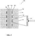
- Fig. 3 illustrates an embodiment of a cross-point memory array 100 that includes a plurality of memory cells 105 that are stacked vertically, word lines 110 and a bit line 120 as described in conjunction with Fig. 2 .
- Cross-point memory array 100 also includes one or more insulating layers 306 that include materials to provide dielectric isolation and increase the thermal resistance between memory cells 105.
- the insulating layer may include oxide or nitride materials, such as silicon oxide (e.g., SiO 2 ), aluminum oxide (e.g., Al 2 O 3 ) and silicon nitride (e.g., Si 3 N 4 ).
- selector devices 210 of memory cells 105 which may also be referred to as memory elements may be coaxial with bit line 120, that is, they may share the same axis of rotation.
- bit line 120 may be cylindrical and the plurality of selector devices 210 may be annular and surround bit line 120.
- a dielectric layer 302 surrounds the bit line 120.
- the dielectric layer 302 is a thin dielectric lamina that can include oxide or nitride materials, such as silicon oxide (SiO 2 ), aluminum oxide (Al 2 O 3 ), hafnium oxide (HfO2) and silicon nitride (Si 3 N 4 ).
- the dielectric layer 302 is a thin layer in the range of 1-2 nanometers to allow the dielectric layer 302 to electrically conduct through a tunnel effect and to prevent possible contamination between the material (for example, tungsten (W)) in the bit line 120 and the material (for example, chalcogenide) in the selector device 210.
- the word line 110 is a conductive line and can comprise three metal layers comprising a conductive material, second conductive layer 312 can comprise Carbon (C) or other conductive material. Second conductive layer 312 is sandwiched between other metal layers 308 that can comprise Tungsten (W) or other conductive material.
- the bit line 120 is a conductive line and can comprise a metal layer as discussed earlier in conjunction with Fig. 2 .
- a dielectric layer 304 surrounding the tip of the word line 110 and adjacent to the selector device 210 includes materials to provide dielectric isolation.
- the insulating layer may include oxide or nitride materials that do not chemically interact with the active chalcogenide material in the selector device 210, such as silicon oxide (SiO 2 ), aluminum oxide (Al 2 O 3 ), hafnium oxide (HfO2) and silicon nitride (Si 3 N 4 ).
- the dielectric layer 304 is about 10 nanometers (nm) thick to provide a bias between the word line (WL) and the bit line (BL).
- the width of the dielectric layer 304 is selected to avoid breakdown, that is to ensure that an electric field between the WL and BL is sustained to avoid an electrical breakdown that can realize a short-circuit between WL and BL.
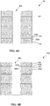
- Fig. 4A and Fig. 4B show various portions of a fabrication process to form a cross-point memory array, according to an embodiment.
- process operations described herein may refer to particular conductor, semiconductor, or dielectric materials, such as silicon, silicon dioxide, silicon nitride, or others, a person of ordinary skill in the art will recognize that other conductor, semiconductor, and dielectric materials may be substituted and still be within a scope of the disclosed subject matter. Thus, the material choices and selections presented are merely provided as an aid in understanding one example of a fabrication process.
- formation and process may refer to one material placed, for example, “over” or “above” another material.
- Such descriptors are relative terms only and obviously depend upon an exact orientation of any resulting device. However, a person of ordinary skill in the art will readily understand the context of such relative terms upon reading and understanding the disclosure provided herein in conjunction with the respective drawings.
- Materials or components in cross-point memory array 100 may be formed by depositing material using chemical vapor deposition, metal-organic chemical vapor deposition, physical vapor deposition, or atomic layer deposition. Material may be removed by etching, such as chemical or plasma etching. First, a source material is formed, and then various materials are formed over the source material
- the cross-point memory array 100 is fabricated on a semiconductor substrate.
- a semiconductor substrate can be any of various types of substrates used in the semiconductor and allied industries, such as silicon wafers, other elemental semiconductor wafers, compound semiconductor wafers, thin film head assemblies, polyethylene-terephthalate (PET) films deposited or otherwise formed with a semiconducting material layer (followed by an annealing activity, such as excimer laser annealing (ELA) in some embodiments), as well as numerous other types of substrates known independently in the art.
- annealing activity such as excimer laser annealing (ELA) in some embodiments
- Insulating layer(s) 306 are formed over the substrate.
- a first conductive layer 308A is formed over the insulating layer(s) 306.
- a second conductive layer 312 is formed over the first conductive layer 308A.
- a third conductive layer 308B is formed over the second conductive layer 312.
- the three conductive layers 308A, 308B and 312 form the word line 110.
- Conductive layers 308A, 308B, and 312, and insulating layer 306 are repeated to form an array of memory cells.
- the first conductive layer 308A and third conductive layer 308B can comprise Tungsten (W) and the second conductive layer 312 can comprise carbon (C).
- a trench is formed by etching a pillar opening 402 through the plurality of layers 306, 308A, 308B, 312 formed on the substrate.
- the pillar opening 402 can be considered to be an opening (for example, an aperture) formed at least partially through the various materials discussed above.
- the pillar opening 402 can be formed by an anisotropic dry etch process (for example, reactive ion etch (RIE) or plasma etch).
- RIE reactive ion etch
- the pillar opening 402 may be formed by one or more various types of chemical etchants (e.g., such as potassium hydroxide (KOH) or tetramethyl ammonium hydroxide (TMAH)), mechanical techniques, other types of ion milling, or laser ablation techniques.
- chemical etchants e.g., such as potassium hydroxide (KOH) or tetramethyl ammonium hydroxide (TMAH)
- mechanical techniques other types of ion milling, or laser ablation techniques.
- the first conductive layer 308A and the third conductive layer 308B are recessed by etching or otherwise having portions removed laterally to form recesses 404A, 404B away from the sidewall of the pillar opening 402.
- the etching of the first conductive layer 308A and the third conductive layer 308B to form recesses 404A, 404B results in the protrusion of the second conductive layer 400 that can be employed as a tip-like contact.
- An insulating material for example, oxide or nitride materials, such as silicon oxide (SiO 2 ), aluminum oxide (Al 2 O 3 ) or silicon nitride (Si 3 N 4 ) is deposited in the recesses 404A, 404B.
- the selector device 210 comprising a chalcogenide material or phase change material is formed on the sidewalls of the pillar opening 402 followed by a dielectric layer 302 being formed adjacent to the selector device 210, the dielectric layer 302 and the chalcogenide material are primarily or entirely formed on opposing faces of the pillar opening 402.
- the remaining trench (or pillar opening) 402 is filled with a conductive material to form the bit line 120 to provide the memory array discussed in conjunction with Fig. 3 .
- the selector device 210 comprising a chalcogenide material and the middle metal second conductive layer 312 comprise different materials which have a different composition and stoichiometry from each other.
- the reduction in contact area between the selector device 210 having a chalcogenide material and the write line 102 through the tip like contact of the middle metal second conductive layer 312 in the write line 102 exacerbates both the electric field and the temperature gradient that are the drivers of the stoichiometry gradient 310 ( Fig. 3 ). This results in increasing the difference ("window") between the threshold voltages.
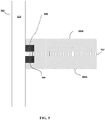
- Fig. 5 shows a portion of a fabrication process to form a cross-point memory array, according to another embodiment.
- the insulating material for example, oxide or nitride materials, such as silicon oxide (SiO 2 ), aluminum oxide (Al 2 O 3 ) or silicon nitride (Si 3 N 4 ) is deposited in the recesses 404A, 404B as described in conjunction with Fig 4A and 4B
- a portion of the second conductive layer 312 is recessed by etching or otherwise having portions removed laterally to form recess 500 away from the sidewall of the pillar opening 402.
- the selector device 210 comprising a chalcogenide material or phase change material formed on the sidewalls of the pillar opening 402 fills the recess 500 resulting in a protrusion of the chalcogenide material adjacent to the tip-like contact of the word line 110.
- This embodiment further increases the difference ("window") between threshold voltages and also allows the diameter of the trench to be reduced because the width of the selector device 210 formed on the sidewalls can be reduced from the embodiment shown in Fig. 4 .
- Fig. 6 shows a portion of a fabrication process to form a cross-point memory array, according to yet another embodiment.
- oxide or nitride materials such as silicon oxide (SiO 2 ), aluminum oxide (Al 2 O 3 ) or silicon nitride (Si 3 N 4 ) is deposited in the recesses 404A, 404B as described in conjunction with Fig 4A and 4B , a portion of the second conductive layer 312 is recessed by etching or otherwise having portions removed laterally.
- the width of the word line 110 is about 30 nanometers
- the width of the insulating material in the insulating layers 306 at top and bottom of the word line 110 is about 30 nanometers
- insulating material in the dielectric layer 304 is about 12 nanometers in height and width.
- the selector device 210 comprising a chalcogenide material or phase change material formed on the sidewalls of the pillar opening 402 fills the funnel shaped recess 600 resulting in a protrusion of the chalcogenide material adjacent to the tip-like contact of the word line 110. This allows a further scaling of the diameter of the trench where the material of the selector device 210 aligns with the insulating material in the insulating layers 306 at top and bottom of the conductive layers 308A, 308B, 312. This embodiment further increases the difference ("window") between threshold voltages.
- Fig. 7 is a flowgraph illustrating a method for forming a tip-contact controlled three dimensional vertical self select memory.
- word line 110 is formed by forming a first conductive layer 308A over insulating layer(s) 306, a second ("middle") conductive layer 312 over the first conductive layer 308A and a third conductive layer 308B over the second conductive layer 312. Processing continues with block 702.
- a recess is etched in the middle second conductive layer 312 to provide a tip contact with a selector device 210 comprising a chalcogenide material and a dielectric layer 304 comprising an insulator material is deposited in the recess. Processing is complete for the embodiment described in conjunction with Figs. 3 and Figs 4A and 4B .
- the middle second conductive layer 312 is etched to provide a recess 500.
- the selector device 210 comprising a chalcogenide material is deposited in the recess 500. Processing is complete for the embodiment described in conjunction with Fig. 5 .
- the insulator material in the dielectric layer 304 is etched to provide a funnel shaped recess 600.
- the selector device 210 comprising a chalcogenide material is deposited in the funnel shaped recess.
- the selector device 210 comprising a chalcogenide material aligns with the dielectric layer 302 at the sidewall of the pillar opening 402. Processing is complete for the embodiment described in conjunction with Fig. 6 .
- Fig. 8 is a block diagram of an embodiment of a computer system 800.
- Computer system 800 may correspond to a computing device including, but not limited to, a server, a workstation computer, a desktop computer, a laptop computer, and/or a tablet computer.
- the computer system 800 includes a system on chip (SOC or SoC) 824 which combines processor, graphics, memory, and Input/Output (I/O) control logic into one SOC package.
- the SOC 104 includes at least one Central Processing Unit (CPU) module 808, a memory controller 814, a Graphics Processor Unit (GPU) 810, and an Input/Output (I/O) System 816.
- each core 802 may internally include one or more instruction/data caches, execution units, prefetch buffers, instruction queues, branch address calculation units, instruction decoders, floating point units, retirement units, etc.
- the CPU 808 may correspond to a single core or a multi-core general purpose processor, according to one embodiment.
- the Graphics Processor Unit (GPU) 810 may include one or more GPU cores and a GPU cache which may store graphics related data for the GPU core.
- the GPU core may internally include one or more execution units and one or more instruction and data caches. Additionally, the GPU 810 may contain other graphics logic units that are not shown in Fig. 8 , such as one or more vertex processing units, rasterization units, media processing units, and codecs.
- one or more I/O adapter(s) 822 are present to translate a host communication protocol utilized within the core(s) 802 to a protocol compatible with particular I/O devices.
- Some of the protocols that adapters may be utilized for translation include Peripheral Component Interconnect (PCI)-Express (PCI-E), 3.0; Universal Serial Bus (USB), 3.0; Serial Advanced Technology Attachment (SATA), 3.0; Small Computer System Interface (SCSI), Ultra-640; and Institute of Electrical and Electronics Engineers (IEEE) 1594 "Firewire.
- PCI Peripheral Component Interconnect
- USB Universal Serial Bus
- SATA Serial Advanced Technology Attachment
- SCSI Small Computer System Interface
- Ultra-640 Institute of Electrical and Electronics Engineers
- the I/O adapter(s) 822 may communicate with external I/O devices 820 which may include, for example, user interface device(s) including a display, a touch-screen display, printer, keypad, keyboard, communication logic, wired and/or wireless, storage device(s) 826 including hard disk drives (“HDD”), solid-state drives (“SSD”), removable storage media, Digital Video Disk (DVD) drive, Compact Disk (CD) drive, Redundant Array of Independent Disks (RAID), tape drive or other storage device. Additionally, there may be one or more wireless protocol I/O adapters. Examples of wireless protocols, among others, are used in personal area networks, such as IEEE 802.15 and Bluetooth, 4.0; wireless local area networks, such as IEEE 802.11-based wireless protocols; and cellular protocols.
- wireless protocols are used in personal area networks, such as IEEE 802.15 and Bluetooth, 4.0; wireless local area networks, such as IEEE 802.11-based wireless protocols; and cellular protocols.
- the memory may be a cross-point memory array 100 that includes a plurality of memory cells as discussed in conjunction with Figs. 3-6 .
- Flow diagrams as illustrated herein provide examples of sequences of various process actions.
- the flow diagrams can indicate operations to be executed by a software or firmware routine, as well as physical operations.
- a flow diagram can illustrate the state of a finite state machine (FSM), which can be implemented in hardware and/or software.
- FSM finite state machine
- FIG. 1 Flow diagrams as illustrated herein provide examples of sequences of various process actions.
- the flow diagrams can indicate operations to be executed by a software or firmware routine, as well as physical operations.
- a flow diagram can illustrate the state of a finite state machine (FSM), which can be implemented in hardware and/or software.
- FSM finite state machine
- the content can be directly executable ("object” or “executable” form), source code, or difference code (“delta” or “patch” code).
- the software content of the embodiments described herein can be provided via an article of manufacture with the content stored thereon, or via a method of operating a communication interface to send data via the communication interface.
- a machine readable storage medium can cause a machine to perform the functions or operations described, and includes any mechanism that stores information in a form accessible by a machine (e.g., computing device, electronic system, etc.), such as recordable/non-recordable media (e.g., read only memory (ROM), random access memory (RAM), magnetic disk storage media, optical storage media, flash memory devices, etc.).
- a communication interface includes any mechanism that interfaces to any of a hardwired, wireless, optical, etc., medium to communicate to another device, such as a memory bus interface, a processor bus interface, an Internet connection, a disk controller, etc.
- the communication interface can be configured by providing configuration parameters and/or sending signals to prepare the communication interface to provide a data signal describing the software content.
- the communication interface can be accessed via one or more commands or signals sent to the communication interface.
- Each component described herein can be a means for performing the operations or functions described.
- Each component described herein includes software, hardware, or a combination of these.
- the components can be implemented as software modules, hardware modules, special-purpose hardware (e.g., application specific hardware, application specific integrated circuits (ASICs), digital signal processors (DSPs), etc.), embedded controllers, hardwired circuitry, etc.
- special-purpose hardware e.g., application specific hardware, application specific integrated circuits (ASICs), digital signal processors (DSPs), etc.
- embedded controllers e.g., hardwired circuitry, etc.
- the present disclosure describes a number of examples.
- Example 1 may be a method of forming a memory, comprising: depositing a first conductive layer comprising a first conductive material; depositing a second conductive layer comprising a second conductive material on top of the second conductive layer; depositing a third conductive layer comprising the first conductive material on top of the second conductive layer; etching a recess in the second conductive layer to provide a tip contact with a selector material; and depositing an insulating material in the recess to form an insulating layer.
- Example 2 may include the method of example 1, further comprising etching the second conductive layer to provide a second recess to deposit the selector material; and depositing the selector material in the second recess.
- Example 3 may include the method of Example 1 and Example 2, further comprising etching a funnel shaped recess by etching a portion of the first conductive layer, a portion of the third conductive layer and a portion of the insulating layer; and depositing the selector material in the funnel shaped recess.
- Example 4 may include the method of Examples 1-2, wherein the selector material is aligned with a dielectric layer adjacent to a sidewall of a pillar opening and the first and second conductive layers.
- Example 5 may include the method of Examples 1-2 wherein the first conductive layer and third conductive layer is tungsten and the second conductive layer is carbon.
- Example 6 may include the method of Examples 1-2 and Example 4, wherein the dielectric layer is aluminum oxide.
- Example 7 may include the method of Examples 1- 2 and Example 4, wherein the dielectric layer is about 10 nanometers (nm) thick.
- Example 8 may be a memory comprising: a first conductive layer comprising a first conductive material; a second conductive layer comprising a second conductive material on top of the second conductive layer; a third conductive layer comprising the first conductive material on top of the second conductive layer; and an insulating layer formed in a recess in the second conductive layer to provide a tip contact with a selector material.
- Example 9 may include the memory of Example 8, further comprising: a selector material formed in a second recess in the second conductive layer.
- Example 10 may include the memory of Example 8 and Example 9, further comprising: a selector material formed in a funnel shaped recess in the first conductive layer, a portion of the third conductive layer and a portion of the insulating layer.
- Example 11 may include the memory of Example 8 and Example 9, wherein the selector material is aligned with a dielectric layer adjacent to a sidewall of a pillar opening and the first and second conductive layers.
- Example 12 may include the memory of Example 8 and Example 9 and Example 11, wherein the insulating layer comprises is aluminum oxide.
- Example 13 may include the memory of Example 8 and Example 9 and Example 11 and Example 12, wherein the insulating layer is about 10 nanometers (nm) thick.
- Example 14 may include a system including a processor; and a memory communicatively coupled to the memory, the memory comprising: a first conductive layer comprising a first conductive material; a second conductive layer comprising a second conductive material on top of the second conductive layer; a third conductive layer comprising the first conductive material on top of the second conductive layer; and an insulating layer formed in a recess in the second conductive layer to provide a tip contact with a selector material.
- Example 15 may include the system of Example 14, further comprising: a selector material formed in a second recess in the second conductive layer.
- Example 16 may include the system of Example 14 and Example 15, further comprising: the selector material formed in a funnel shaped recess in the first conductive layer, a portion of the third conductive layer and a portion of the insulating layer.
- Example 17 may include the system of Example 14 and Example 15, wherein the selector material is aligned with a dielectric layer adjacent to a sidewall of a pillar opening and the first and second conductive layers.
- Example 18 may include the system of Example 14 and Example 15 and Example 17, wherein the dielectric layer comprises aluminum oxide.
- Example 19 may include the system of Example 14 and Example 15 and Example 17, wherein the dielectric layer is about 10 nanometers (nm) thick.
- Example 20 may include a device comprising means to perform any one of Examples 1 to 7.
Landscapes
- Engineering & Computer Science (AREA)
- Manufacturing & Machinery (AREA)
- Chemical & Material Sciences (AREA)
- Crystallography & Structural Chemistry (AREA)
- Semiconductor Memories (AREA)
Abstract
Description
- This disclosure relates to memory devices and in particular to three dimensional (3D) vertical Self Select Memory (SSM).
- A memory device may include variable resistance memory cells which can be switched between high and low resistance states in direct or indirect response to an electrical signal, such as a voltage or a current pulse. A program operation also referred to as a RESET operation can change the resistance state of the memory cell from a relatively low resistance state to a relatively high resistance state. Similarly, an erase operation, also referred to as a SET operation, can change the resistance state of the memory cell from a relatively high resistance state to a relatively low resistance state.
- Features of embodiments of the claimed subject matter will become apparent as the following detailed description proceeds, and upon reference to the drawings, in which like numerals depict like parts, and in which:
-
FIG. 1 is an embodiment of a cross point memory array that includes a plurality of memory cells; -
Fig. 2 is a portion of an embodiment of the cross-point memory array shown inFig. 1 ; -
Fig. 3 illustrates an embodiment of a memory array that includes a plurality of memory cells that are stacked vertically, word lines and a bit line as described in conjunction withFig. 2 ; -
Fig. 4A and Fig. 4B show various portions of a fabrication process to form a cross-point memory array, according to an embodiment; -
Fig. 5 shows a portion of a fabrication process to form a cross-point memory array, according to another embodiment; -
Fig. 6 shows a portion of a fabrication process to form a cross-point memory array, according to yet another embodiment; -
Fig. 7 is a flowgraph illustrating a method for forming a tip-contact controlled three dimensional vertical self select memory; and -
Fig. 8 is a block diagram of an embodiment of a computer system 800 that includes a tip-contact controlled three dimensional vertical self select memory. - Although the following Detailed Description will proceed with reference being made to illustrative embodiments of the claimed subject matter, many alternatives, modifications, and variations thereof will be apparent to those skilled in the art. Accordingly, it is intended that the claimed subject matter be viewed broadly, and be defined only as set forth in the accompanying claims.
- The variable resistance memory cells may be arranged in a cross-point array configuration with memory cells disposed and electrically connected at intersections between a first set of conductive lines (word lines) and a second set of conductive lines (bit lines) overlapping and crossing the first set of conductive lines.
- One category of a variable resistance memory cells is a phase change memory cell. The electrical resistance of the phase change material in the memory cell can be changed by electrical signals provided through the word and bit lines. The variable resistance memory cell may be a low resistance crystalline state or a high resistance amorphous state, the state is used to represent whether the memory cell stores a logic (binary) '1' or logic (binary) '0'.
- The logic state of the memory cell is detected by observing a threshold voltage at which the memory cell conducts current when the memory cell is read. A small difference between the threshold voltages may result in the incorrect logic state being read.
- In an embodiment, the difference ("window") between threshold voltages is increased by amplifying the stoichiometry gradient by means an asymmetry in the cell architecture to provide a greater threshold voltage margin for detecting the different logic states.
- Reference in the specification to "one embodiment" or "an embodiment" means that a particular feature, structure, or characteristic described in conjunction with the embodiment can be included in at least one embodiment of the invention. The appearances of the phrase "in one embodiment" in various places in the specification do not necessarily all refer to the same embodiment.
-
Fig. 1 is an embodiment of across-point memory array 100 that includes a plurality ofmemory cells 105. In an embodiment, eachmemory cell 105 includes a material with a crystalline or an amorphous atomic configuration that may have different electrical resistances. A voltage applied to thememory cell 105 results in a different current dependent on whether the material is in a crystalline or an amorphous state, and the magnitude of the resulting current may be used to determine the logic state stored bymemory cell 105. -
Cross-point memory array 100 may be a three dimensional (3D) memory array that includes a plurality of levels of two-dimensional (2D) memory arrays formed on top of one another and separated by an electrically insulating material. In the embodiment shown inFig. 1 ,cross-point memory array 100 includes three levels; however, the number of levels is not limited to three. The electrically insulating material may be thermally insulating and may contain multiple sublayers to increase the thermal resistance between each level. Each level may be aligned or positioned so thatmemory cells 105 may be approximately aligned with one another across each level, forming amemory cell stack 145. - Each row of
memory cells 105 is connected to aword line 110, and each column ofmemory cells 105 is connected to abit line 115 with amemory cell 105 located at the intersection of aword line 110 and abit line 115. In an embodiment,word lines 110 andbit lines 115 may be substantially perpendicular to one another to create an array. - The
memory cells 105 can function in a two-terminal architecture with aparticular word line 110 andbit line 115 serving as the electrodes for thememory cells 105. Eachmemory cell 105 can be addressed individually allowing data to be written and read on a per-bit basis.Word lines 110 andbit lines 115 may be made of conductive materials, such as metals (for example, copper, aluminum, gold, tungsten, titanium), metal alloys, carbon, or other conductive materials, alloys, or compounds. - In operation, a
memory cell 105 ofcross-point memory array 100 can be written by applying a voltage, across thememory cell 105 via aselected word line 110 andbit line 115. Amemory cell 105 ofcross-point memory array 100 can be read by sensing current on abit line 115 corresponding to therespective memory cell 105 responsive to a particular voltage applied to theselected word line 110 to which the respective memory cell is coupled. - The magnitude of the current sensed is dependent on the electrical resistance of the memory cell 1 05 and may be used to differentiate between the electrically resistive states of the phase change material. In some cases, sensing may depend on a threshold voltage Vth, a voltage at which point a current begins to flow.
- The state of the
memory cell 105 may be a low resistance crystalline state or a high resistance amorphous state, the state is used to represent whether the memory cell stores a logic (binary) '1' or logic (binary) '0'. In an embodiment, the low resistance state represents a logic '0' and the high resistance state represents a logic '1'. -
Fig. 2 is a portion of an embodiment of thecross-point memory array 100 shown inFig. 1 including any one of thememory cells 105 in thecross-point memory array 100. As shown inFig. 2 , theword line 110 extends parallel to the plane of the page, and thebit line 115 extends into the plane of the page, perpendicular to theword line 110. A memory cell 1 05 may be located at an intersection of theword line 110 and thebit line 115. - The
memory cell 105 may be configured as a two-terminal device between thebit line 115 andword line 110 in some embodiments. A first logic state may be written to thememory cell 105 by applying a voltage (for example, a write pulse) across thememory cell 105 in a first polarity. A second logic state may be written to thememory cell 105 by applying a voltage (for example, a write pulse) across thememory cell 105 in a second polarity, which may be opposite to the first polarity. Thememory cell 105 is read by applying a voltage (for example, a read pulse) across the terminals. In some embodiments, thememory cell 105 is read by applying a voltage across thememory cell 105 in the first polarity. In other embodiments, thememory cell 105 is read by applying a voltage across thememory cell 105 in the second polarity. Thememory cell 105 may always be read with the same polarity. When thememory cell 105 is read with a voltage in the same voltage polarity with which thememory cell 105 was written, thememory cell 105 may exhibit a first threshold voltage VTH. When thememory cell 105 is read with a voltage in the opposite voltage polarity with which thememory cell 105 was written, the memory cell may exhibit a second threshold voltage VTH. The different threshold voltages may be used to represent different logic states. - The
bit line 115 andword line 110 are conductive lines and can comprise a metal. Examples of the metal include elemental metals such as Al, Cu, Ni, Cr, Co, Ru, Rh, Pd, Ag, Pt, Au, Jr, Ta, and W; conductive metal nitrides such as TiN, TaN, WN, and TaCN; conductive metal silicides such as tantalum silicides, tungsten silicides, nickel silicides, cobalt silicides and titanium silicides; and conductive metal oxides such as RuO2. - In the embodiment shown, the
memory cell 105 is formed as a memory cell pillar disposed at an intersection between abit line 115 and aword line 110. Eachmemory cell 105 comprises a first active element comprising a storage material ("storage element") 206 disposed over thebit line 115 and a second active element comprising a selector material ("selector device") 210 disposed over theselector device 210. In embodiments where thememory cell 105 is a phase change memory cell, thestorage element 206 can include a chalcogenide material that is configured to switch between crystalline and amorphous phases via an electrical pulse applied between thebit line 115 and theword line 110 during an access operation, such as a write access operation. In some embodiments, the chalcogenide material may be a phase change material, but other materials may be used. In some embodiments, thestorage element 206 includes a chalcogenide material such as an alloy including at least two of the elements within the indium(In)-antimony(Sb)-tellurium(Te) (IST) alloy system, e.g., In2Sb2Te5, In1Sb2Te4, In1Sb4Te7, etc., or an alloy including at least two of the elements within the germanium(Ge)-antimony(Sb)-tellurium(Te) (GST) alloy system, e.g., Ge8Sb5Te8, Ge2Sb2Te5, Ge1Sb2Te4, Ge1Sb4Te7, Ge4Sb4Te7, etc. - In other embodiments, the
storage element 206 can be a resistive random access memory (RRAM) storage element (for example, NiO, HfO2, ZrO2, Cu2O, TaO2, Ta2O5, TiO2, SiO2, Al2O3), a conductive bridge random access memory (CBRAM) storage element (for example, metal-doped chalcogenide), and/or a spin transfer torque random access memory (STT-RAM) storage element. - The
storage element 206 may be written and read by varying the voltage to theselector device 210. Theselector device 210 may include a two terminal device (for example, a switch), such as a diode, an ovonic threshold switch (OTS), a tunnel junction, or a mixed ionic electronic conduction switch (MIEC). - In some embodiments, the
selector device 210 may also include a layer of chalcogenide material. A selector device having a chalcogenide material can sometimes be referred to as an Ovonic Threshold Switch (OTS). An OTS may include a chalcogenide composition including any one of the chalcogenide alloy systems described above for the storage element and, in addition, further include an element that can suppress crystallization, such as arsenic (As), nitrogen (N) and carbon (C), to name a few. Examples of OTS materials include Te-As-Ge-Si, Ge-Te-Pb, Ge-Se-Te, Al-As-Te, Se-As-Ge-Si, Se-As-Ge-C, Se-Te-Ge-Si, Ge-Sb-Te-Se, Ge-Bi-Te-Se, Ge-As-Sb-Se, Ge-As-Bi-Te, and Ge-As-Bi-Se. - The
memory cell 105 can additionally include one or more dielectric layers (not shown) that may be formed between the bit line, word line, theselector device 210 and thestorage element 206. When included, one or more of the dielectric layers can include a material, such as carbon, that can serve simultaneously as an electrode material that can provide relatively low contact resistance between adjacent materials, as well as a diffusion barrier against intermixing, for example, between metal lines and chalcogenide elements, or between chalcogenide elements of different compositions. -
Fig. 3 illustrates an embodiment of across-point memory array 100 that includes a plurality ofmemory cells 105 that are stacked vertically,word lines 110 and abit line 120 as described in conjunction withFig. 2 .Cross-point memory array 100 also includes one or moreinsulating layers 306 that include materials to provide dielectric isolation and increase the thermal resistance betweenmemory cells 105. The insulating layer may include oxide or nitride materials, such as silicon oxide (e.g., SiO2), aluminum oxide (e.g., Al2O3) and silicon nitride (e.g., Si3N4). - In an embodiment,
selector devices 210 ofmemory cells 105 which may also be referred to as memory elements may be coaxial withbit line 120, that is, they may share the same axis of rotation. For example,bit line 120 may be cylindrical and the plurality ofselector devices 210 may be annular andsurround bit line 120. - In the embodiment shown, a
dielectric layer 302 surrounds thebit line 120. Thedielectric layer 302 is a thin dielectric lamina that can include oxide or nitride materials, such as silicon oxide (SiO2), aluminum oxide (Al2O3), hafnium oxide (HfO2) and silicon nitride (Si3N4). In an embodiment, thedielectric layer 302 is a thin layer in the range of 1-2 nanometers to allow thedielectric layer 302 to electrically conduct through a tunnel effect and to prevent possible contamination between the material (for example, tungsten (W)) in thebit line 120 and the material (for example, chalcogenide) in theselector device 210.
Theword line 110 is a conductive line and can comprise three metal layers comprising a conductive material, secondconductive layer 312 can comprise Carbon (C) or other conductive material. Secondconductive layer 312 is sandwiched betweenother metal layers 308 that can comprise Tungsten (W) or other conductive material. Thebit line 120 is a conductive line and can comprise a metal layer as discussed earlier in conjunction withFig. 2 . - A
dielectric layer 304 surrounding the tip of theword line 110 and adjacent to theselector device 210 includes materials to provide dielectric isolation. The insulating layer may include oxide or nitride materials that do not chemically interact with the active chalcogenide material in theselector device 210, such as silicon oxide (SiO2), aluminum oxide (Al2O3), hafnium oxide (HfO2) and silicon nitride (Si3N4). In an embodiment, thedielectric layer 304 is about 10 nanometers (nm) thick to provide a bias between the word line (WL) and the bit line (BL). The width of thedielectric layer 304 is selected to avoid breakdown, that is to ensure that an electric field between the WL and BL is sustained to avoid an electrical breakdown that can realize a short-circuit between WL and BL. -
Fig. 4A and Fig. 4B show various portions of a fabrication process to form a cross-point memory array, according to an embodiment. - Although the process operations described herein may refer to particular conductor, semiconductor, or dielectric materials, such as silicon, silicon dioxide, silicon nitride, or others, a person of ordinary skill in the art will recognize that other conductor, semiconductor, and dielectric materials may be substituted and still be within a scope of the disclosed subject matter. Thus, the material choices and selections presented are merely provided as an aid in understanding one example of a fabrication process.
- Further, formation and process may refer to one material placed, for example, "over" or "above" another material. Such descriptors are relative terms only and obviously depend upon an exact orientation of any resulting device. However, a person of ordinary skill in the art will readily understand the context of such relative terms upon reading and understanding the disclosure provided herein in conjunction with the respective drawings.
- Materials or components in
cross-point memory array 100 may be formed by depositing material using chemical vapor deposition, metal-organic chemical vapor deposition, physical vapor deposition, or atomic layer deposition. Material may be removed by etching, such as chemical or plasma etching. First, a source material is formed, and then various materials are formed over the source material - The
cross-point memory array 100 is fabricated on a semiconductor substrate. A semiconductor substrate can be any of various types of substrates used in the semiconductor and allied industries, such as silicon wafers, other elemental semiconductor wafers, compound semiconductor wafers, thin film head assemblies, polyethylene-terephthalate (PET) films deposited or otherwise formed with a semiconducting material layer (followed by an annealing activity, such as excimer laser annealing (ELA) in some embodiments), as well as numerous other types of substrates known independently in the art. - Insulating layer(s) 306 are formed over the substrate. A first
conductive layer 308A is formed over the insulating layer(s) 306. A secondconductive layer 312 is formed over the firstconductive layer 308A. A thirdconductive layer 308B is formed over the secondconductive layer 312. The threeconductive layers word line 110.Conductive layers layer 306 are repeated to form an array of memory cells. As discussed earlier, in an embodiment, the firstconductive layer 308A and thirdconductive layer 308B can comprise Tungsten (W) and the secondconductive layer 312 can comprise carbon (C). - After all layers have been formed, a trench is formed by etching a pillar opening 402 through the plurality of
layers - The first
conductive layer 308A and the thirdconductive layer 308B are recessed by etching or otherwise having portions removed laterally to formrecesses pillar opening 402. The etching of the firstconductive layer 308A and the thirdconductive layer 308B to formrecesses - An insulating material (dielectric), for example, oxide or nitride materials, such as silicon oxide (SiO2), aluminum oxide (Al2O3) or silicon nitride (Si3N4) is deposited in the
recesses selector device 210 comprising a chalcogenide material or phase change material is formed on the sidewalls of the pillar opening 402 followed by adielectric layer 302 being formed adjacent to theselector device 210, thedielectric layer 302 and the chalcogenide material are primarily or entirely formed on opposing faces of thepillar opening 402. The remaining trench (or pillar opening) 402 is filled with a conductive material to form thebit line 120 to provide the memory array discussed in conjunction withFig. 3 . - The
selector device 210 comprising a chalcogenide material and the middle metal secondconductive layer 312 comprise different materials which have a different composition and stoichiometry from each other. The reduction in contact area between theselector device 210 having a chalcogenide material and the write line 102 through the tip like contact of the middle metal secondconductive layer 312 in the write line 102 exacerbates both the electric field and the temperature gradient that are the drivers of the stoichiometry gradient 310 (Fig. 3 ). This results in increasing the difference ("window") between the threshold voltages. -
Fig. 5 shows a portion of a fabrication process to form a cross-point memory array, according to another embodiment. In the embodiment shown inFig. 5 , after the insulating material (dielectric), for example, oxide or nitride materials, such as silicon oxide (SiO2), aluminum oxide (Al2O3) or silicon nitride (Si3N4) is deposited in therecesses Fig 4A and 4B , a portion of the secondconductive layer 312 is recessed by etching or otherwise having portions removed laterally to formrecess 500 away from the sidewall of thepillar opening 402. Theselector device 210 comprising a chalcogenide material or phase change material formed on the sidewalls of the pillar opening 402 fills therecess 500 resulting in a protrusion of the chalcogenide material adjacent to the tip-like contact of theword line 110. - This embodiment further increases the difference ("window") between threshold voltages and also allows the diameter of the trench to be reduced because the width of the
selector device 210 formed on the sidewalls can be reduced from the embodiment shown inFig. 4 . -
Fig. 6 shows a portion of a fabrication process to form a cross-point memory array, according to yet another embodiment. In the embodiment shown inFig. 6 , after the insulating material in thedielectric layer 304, for example, oxide or nitride materials, such as silicon oxide (SiO2), aluminum oxide (Al2O3) or silicon nitride (Si3N4) is deposited in therecesses Fig 4A and 4B , a portion of the secondconductive layer 312 is recessed by etching or otherwise having portions removed laterally. In addition, a portion of the insulator material in thedielectric layer 304 and the dielectric material in the insulatinglayers 306 is recessed by etching or otherwise having portions removed laterally to form funnel shapedrecess 600 away from the sidewall of thepillar opening 402. In an embodiment, the width of theword line 110 is about 30 nanometers, the width of the insulating material in the insulatinglayers 306 at top and bottom of theword line 110 is about 30 nanometers, and insulating material in thedielectric layer 304 is about 12 nanometers in height and width. - The
selector device 210 comprising a chalcogenide material or phase change material formed on the sidewalls of the pillar opening 402 fills the funnel shapedrecess 600 resulting in a protrusion of the chalcogenide material adjacent to the tip-like contact of theword line 110. This allows a further scaling of the diameter of the trench where the material of theselector device 210 aligns with the insulating material in the insulatinglayers 306 at top and bottom of theconductive layers -
Fig. 7 is a flowgraph illustrating a method for forming a tip-contact controlled three dimensional vertical self select memory. - At
block 700, as discussed in conjunction withFigs. 3 andFigs 4A and 4B ,word line 110 is formed by forming a firstconductive layer 308A over insulating layer(s) 306, a second ("middle")conductive layer 312 over the firstconductive layer 308A and a thirdconductive layer 308B over the secondconductive layer 312. Processing continues withblock 702. - At
block 702, a recess is etched in the middle secondconductive layer 312 to provide a tip contact with aselector device 210 comprising a chalcogenide material and adielectric layer 304 comprising an insulator material is deposited in the recess. Processing is complete for the embodiment described in conjunction withFigs. 3 andFigs 4A and 4B . - At
block 704, the middle secondconductive layer 312 is etched to provide arecess 500. Theselector device 210 comprising a chalcogenide material is deposited in therecess 500. Processing is complete for the embodiment described in conjunction withFig. 5 . - At
block 706, the insulator material in thedielectric layer 304 is etched to provide a funnel shapedrecess 600. Theselector device 210 comprising a chalcogenide material is deposited in the funnel shaped recess. Theselector device 210 comprising a chalcogenide material aligns with thedielectric layer 302 at the sidewall of thepillar opening 402. Processing is complete for the embodiment described in conjunction withFig. 6 . -
Fig. 8 is a block diagram of an embodiment of a computer system 800. Computer system 800 may correspond to a computing device including, but not limited to, a server, a workstation computer, a desktop computer, a laptop computer, and/or a tablet computer. - The computer system 800 includes a system on chip (SOC or SoC) 824 which combines processor, graphics, memory, and Input/Output (I/O) control logic into one SOC package. The SOC 104 includes at least one Central Processing Unit (CPU)
module 808, amemory controller 814, a Graphics Processor Unit (GPU) 810, and an Input/Output (I/O)System 816. Although not shown, each core 802 may internally include one or more instruction/data caches, execution units, prefetch buffers, instruction queues, branch address calculation units, instruction decoders, floating point units, retirement units, etc. TheCPU 808 may correspond to a single core or a multi-core general purpose processor, according to one embodiment. - The Graphics Processor Unit (GPU) 810 may include one or more GPU cores and a GPU cache which may store graphics related data for the GPU core. The GPU core may internally include one or more execution units and one or more instruction and data caches. Additionally, the GPU 810 may contain other graphics logic units that are not shown in
Fig. 8 , such as one or more vertex processing units, rasterization units, media processing units, and codecs. - Within the I/
O subsystem 816, one or more I/O adapter(s) 822 are present to translate a host communication protocol utilized within the core(s) 802 to a protocol compatible with particular I/O devices. Some of the protocols that adapters may be utilized for translation include Peripheral Component Interconnect (PCI)-Express (PCI-E), 3.0; Universal Serial Bus (USB), 3.0; Serial Advanced Technology Attachment (SATA), 3.0; Small Computer System Interface (SCSI), Ultra-640; and Institute of Electrical and Electronics Engineers (IEEE) 1594 "Firewire. - The I/O adapter(s) 822 may communicate with external I/
O devices 820 which may include, for example, user interface device(s) including a display, a touch-screen display, printer, keypad, keyboard, communication logic, wired and/or wireless, storage device(s) 826 including hard disk drives ("HDD"), solid-state drives ("SSD"), removable storage media, Digital Video Disk (DVD) drive, Compact Disk (CD) drive, Redundant Array of Independent Disks (RAID), tape drive or other storage device. Additionally, there may be one or more wireless protocol I/O adapters. Examples of wireless protocols, among others, are used in personal area networks, such as IEEE 802.15 and Bluetooth, 4.0; wireless local area networks, such as IEEE 802.11-based wireless protocols; and cellular protocols. - The memory may be a
cross-point memory array 100 that includes a plurality of memory cells as discussed in conjunction withFigs. 3-6 . - Flow diagrams as illustrated herein provide examples of sequences of various process actions. The flow diagrams can indicate operations to be executed by a software or firmware routine, as well as physical operations. In one embodiment, a flow diagram can illustrate the state of a finite state machine (FSM), which can be implemented in hardware and/or software. Although shown in a particular sequence or order, unless otherwise specified, the order of the actions can be modified. Thus, the illustrated embodiments should be understood only as an example, and the process can be performed in a different order, and some actions can be performed in parallel. Additionally, one or more actions can be omitted in various embodiments; thus, not all actions are required in every embodiment. Other process flows are possible.
- To the extent various operations or functions are described herein, they can be described or defined as software code, instructions, configuration, and/or data. The content can be directly executable ("object" or "executable" form), source code, or difference code ("delta" or "patch" code). The software content of the embodiments described herein can be provided via an article of manufacture with the content stored thereon, or via a method of operating a communication interface to send data via the communication interface. A machine readable storage medium can cause a machine to perform the functions or operations described, and includes any mechanism that stores information in a form accessible by a machine (e.g., computing device, electronic system, etc.), such as recordable/non-recordable media (e.g., read only memory (ROM), random access memory (RAM), magnetic disk storage media, optical storage media, flash memory devices, etc.). A communication interface includes any mechanism that interfaces to any of a hardwired, wireless, optical, etc., medium to communicate to another device, such as a memory bus interface, a processor bus interface, an Internet connection, a disk controller, etc. The communication interface can be configured by providing configuration parameters and/or sending signals to prepare the communication interface to provide a data signal describing the software content. The communication interface can be accessed via one or more commands or signals sent to the communication interface.
- Various components described herein can be a means for performing the operations or functions described. Each component described herein includes software, hardware, or a combination of these. The components can be implemented as software modules, hardware modules, special-purpose hardware (e.g., application specific hardware, application specific integrated circuits (ASICs), digital signal processors (DSPs), etc.), embedded controllers, hardwired circuitry, etc.
- Besides what is described herein, various modifications can be made to the disclosed embodiments and implementations without departing from their scope.
- Therefore, the illustrations and examples herein should be construed in an illustrative, and not a restrictive sense. The scope of the invention should be measured solely by reference to the claims that follow.
- According to various embodiments, the present disclosure describes a number of examples.
- Example 1 may be a method of forming a memory, comprising: depositing a first conductive layer comprising a first conductive material; depositing a second conductive layer comprising a second conductive material on top of the second conductive layer; depositing a third conductive layer comprising the first conductive material on top of the second conductive layer; etching a recess in the second conductive layer to provide a tip contact with a selector material; and depositing an insulating material in the recess to form an insulating layer.
- Example 2 may include the method of example 1, further comprising etching the second conductive layer to provide a second recess to deposit the selector material; and depositing the selector material in the second recess.
- Example 3 may include the method of Example 1 and Example 2, further comprising etching a funnel shaped recess by etching a portion of the first conductive layer, a portion of the third conductive layer and a portion of the insulating layer; and depositing the selector material in the funnel shaped recess.
- Example 4 may include the method of Examples 1-2, wherein the selector material is aligned with a dielectric layer adjacent to a sidewall of a pillar opening and the first and second conductive layers.
- Example 5 may include the method of Examples 1-2 wherein the first conductive layer and third conductive layer is tungsten and the second conductive layer is carbon.
- Example 6 may include the method of Examples 1-2 and Example 4, wherein the dielectric layer is aluminum oxide.
- Example 7 may include the method of Examples 1- 2 and Example 4, wherein the dielectric layer is about 10 nanometers (nm) thick.
- Example 8 may be a memory comprising: a first conductive layer comprising a first conductive material; a second conductive layer comprising a second conductive material on top of the second conductive layer; a third conductive layer comprising the first conductive material on top of the second conductive layer; and an insulating layer formed in a recess in the second conductive layer to provide a tip contact with a selector material.
- Example 9 may include the memory of Example 8, further comprising: a selector material formed in a second recess in the second conductive layer.
- Example 10 may include the memory of Example 8 and Example 9, further comprising: a selector material formed in a funnel shaped recess in the first conductive layer, a portion of the third conductive layer and a portion of the insulating layer.
- Example 11 may include the memory of Example 8 and Example 9, wherein the selector material is aligned with a dielectric layer adjacent to a sidewall of a pillar opening and the first and second conductive layers.
- Example 12 may include the memory of Example 8 and Example 9 and Example 11, wherein the insulating layer comprises is aluminum oxide.
- Example 13 may include the memory of Example 8 and Example 9 and Example 11 and Example 12, wherein the insulating layer is about 10 nanometers (nm) thick.
- Example 14 may include a system including a processor; and a memory communicatively coupled to the memory, the memory comprising: a first conductive layer comprising a first conductive material; a second conductive layer comprising a second conductive material on top of the second conductive layer; a third conductive layer comprising the first conductive material on top of the second conductive layer; and an insulating layer formed in a recess in the second conductive layer to provide a tip contact with a selector material.
- Example 15 may include the system of Example 14, further comprising: a selector material formed in a second recess in the second conductive layer.
- Example 16 may include the system of Example 14 and Example 15, further comprising: the selector material formed in a funnel shaped recess in the first conductive layer, a portion of the third conductive layer and a portion of the insulating layer.
- Example 17 may include the system of Example 14 and Example 15, wherein the selector material is aligned with a dielectric layer adjacent to a sidewall of a pillar opening and the first and second conductive layers.
- Example 18 may include the system of Example 14 and Example 15 and Example 17, wherein the dielectric layer comprises aluminum oxide.
- Example 19 may include the system of Example 14 and Example 15 and Example 17, wherein the dielectric layer is about 10 nanometers (nm) thick.
- Example 20 may include a device comprising means to perform any one of Examples 1 to 7.
Claims (13)
- A method of forming a memory comprising:depositing a first conductive layer comprising a first conductive material;depositing a second conductive layer comprising a second conductive material on top of the second conductive layer;depositing a third conductive layer comprising the first conductive material on top of the second conductive layer;etching a recess in the second conductive layer to provide a tip contact with a selector material; anddepositing an insulating material in the recess to form an insulating layer.
- The method of claim 1, further comprising:etching the second conductive layer to provide a second recess to deposit the selector material; anddepositing the selector material in the second recess.
- The method of claim 2, further comprising:etching a funnel shaped recess by etching a portion of the first conductive layer, a portion of the third conductive layer and a portion of the insulating layer; anddepositing the selector material in the funnel shaped recess.
- The method of claim 2, wherein the selector material is aligned with a dielectric layer adjacent to a sidewall of a pillar opening and the first and second conductive layers.
- The method of claim 2, wherein the first conductive layer and third conductive layer is tungsten and the second conductive layer is carbon.
- The method of claim 4, wherein the dielectric layer is aluminum oxide.
- The method of claim 4, wherein the dielectric layer is about 10 nanometers (nm) thick.
- A memory comprising:a first conductive layer comprising a first conductive material;a second conductive layer comprising a second conductive material on top of the second conductive layer;a third conductive layer comprising the first conductive material on top of the second conductive layer; andan insulating layer formed in a recess in the second conductive layer to provide a tip contact with a selector material.
- The memory of claim 8, further comprising:
a selector material formed in a second recess in the second conductive layer. - The memory of claim 9, further comprising:
selector material formed in a funnel shaped recess in the first conductive layer, a portion of the third conductive layer and a portion of the insulating layer. - The memory of claim 9, wherein the selector material is aligned with a dielectric layer adjacent to a sidewall of a pillar opening and the first and second conductive layers.
- The memory of claim 11, wherein the insulating layer comprises is aluminum oxide.
- The memory of claim 12, wherein the insulating layer is about 10 nanometers (nm) thick.
Applications Claiming Priority (1)
| Application Number | Priority Date | Filing Date | Title |
|---|---|---|---|
| US15/853,697 US10475995B2 (en) | 2017-12-22 | 2017-12-22 | Tip-contact controlled three dimensional (3D) vertical self select memory |
Publications (3)
| Publication Number | Publication Date |
|---|---|
| EP3503232A1 true EP3503232A1 (en) | 2019-06-26 |
| EP3503232B1 EP3503232B1 (en) | 2021-03-31 |
| EP3503232B8 EP3503232B8 (en) | 2021-06-02 |
Family
ID=64899215
Family Applications (1)
| Application Number | Title | Priority Date | Filing Date |
|---|---|---|---|
| EP18214280.2A Active EP3503232B8 (en) | 2017-12-22 | 2018-12-19 | Three-dimensional variable resistance memory with tip contacts |
Country Status (2)
| Country | Link |
|---|---|
| US (1) | US10475995B2 (en) |
| EP (1) | EP3503232B8 (en) |
Families Citing this family (8)
| Publication number | Priority date | Publication date | Assignee | Title |
|---|---|---|---|---|
| US9947721B2 (en) * | 2016-04-01 | 2018-04-17 | Micron Technology, Inc. | Thermal insulation for three-dimensional memory arrays |
| JP2019160981A (en) * | 2018-03-13 | 2019-09-19 | 東芝メモリ株式会社 | Magnetic storage device |
| US11864475B2 (en) * | 2021-05-27 | 2024-01-02 | Micron Technology, Inc. | Memory device with laterally formed memory cells |
| US11812675B2 (en) * | 2021-09-21 | 2023-11-07 | International Business Machines Corporation | Filament confinement in resistive random access memory |
| US12125540B2 (en) * | 2022-04-29 | 2024-10-22 | Micron Technology, Inc. | Write latency and energy using asymmetric cell design |
| US12295147B2 (en) | 2022-04-29 | 2025-05-06 | Micron Technology, Inc. | Asymmetric memory cell design |
| KR20230154552A (en) | 2022-05-02 | 2023-11-09 | 삼성전자주식회사 | Semiconductor memory device |
| KR102887938B1 (en) | 2022-05-25 | 2025-11-19 | 삼성전자주식회사 | Self-selecting memory devices |
Citations (5)
| Publication number | Priority date | Publication date | Assignee | Title |
|---|---|---|---|---|
| US20110177666A1 (en) * | 2009-08-03 | 2011-07-21 | Katsuya Nozawa | Method of manufacturing semiconductor memory |
| US20130153846A1 (en) * | 2011-12-19 | 2013-06-20 | Macronix International Co., Ltd. | Three dimensional memory array adjacent to trench sidewalls |
| US20130229846A1 (en) * | 2010-12-14 | 2013-09-05 | Sandisk 3D Llc | Memories with Cylindrical Read/Write Stacks |
| US20140061574A1 (en) * | 2012-08-31 | 2014-03-06 | Micron Technology, Inc. | Three dimensional memory array architecture |
| US9741768B1 (en) * | 2016-03-31 | 2017-08-22 | Sandisk Technologies Llc | Controlling memory cell size in three dimensional nonvolatile memory |
Family Cites Families (6)
| Publication number | Priority date | Publication date | Assignee | Title |
|---|---|---|---|---|
| US7361585B2 (en) * | 2004-12-23 | 2008-04-22 | Advantech Global, Ltd | System for and method of planarizing the contact region of a via by use of a continuous inline vacuum deposition |
| KR20100048610A (en) * | 2008-10-31 | 2010-05-11 | 삼성전자주식회사 | Semiconductor fackage and forming method of the same |
| US9852941B2 (en) * | 2014-10-03 | 2017-12-26 | Analog Devices, Inc. | Stacked conductor structure and methods for manufacture of same |
| US9748311B2 (en) | 2014-11-07 | 2017-08-29 | Micron Technology, Inc. | Cross-point memory and methods for fabrication of same |
| US9379321B1 (en) | 2015-03-20 | 2016-06-28 | Intel Corporation | Chalcogenide glass composition and chalcogenide switch devices |
| US9947721B2 (en) | 2016-04-01 | 2018-04-17 | Micron Technology, Inc. | Thermal insulation for three-dimensional memory arrays |
-
2017
- 2017-12-22 US US15/853,697 patent/US10475995B2/en active Active
-
2018
- 2018-12-19 EP EP18214280.2A patent/EP3503232B8/en active Active
Patent Citations (5)
| Publication number | Priority date | Publication date | Assignee | Title |
|---|---|---|---|---|
| US20110177666A1 (en) * | 2009-08-03 | 2011-07-21 | Katsuya Nozawa | Method of manufacturing semiconductor memory |
| US20130229846A1 (en) * | 2010-12-14 | 2013-09-05 | Sandisk 3D Llc | Memories with Cylindrical Read/Write Stacks |
| US20130153846A1 (en) * | 2011-12-19 | 2013-06-20 | Macronix International Co., Ltd. | Three dimensional memory array adjacent to trench sidewalls |
| US20140061574A1 (en) * | 2012-08-31 | 2014-03-06 | Micron Technology, Inc. | Three dimensional memory array architecture |
| US9741768B1 (en) * | 2016-03-31 | 2017-08-22 | Sandisk Technologies Llc | Controlling memory cell size in three dimensional nonvolatile memory |
Also Published As
| Publication number | Publication date |
|---|---|
| US20190044062A1 (en) | 2019-02-07 |
| EP3503232B8 (en) | 2021-06-02 |
| EP3503232B1 (en) | 2021-03-31 |
| US10475995B2 (en) | 2019-11-12 |
Similar Documents
| Publication | Publication Date | Title |
|---|---|---|
| EP3503232B1 (en) | Three-dimensional variable resistance memory with tip contacts | |
| KR102153464B1 (en) | Vertical cross-point embedded memory architecture for metal-conductive oxide-metal(mcom) memory elements | |
| JP7230051B2 (en) | Self-selecting memory array with horizontal access lines | |
| JP4830275B2 (en) | Memory element | |
| CN102779827B (en) | Storage without isolation | |
| TWI593087B (en) | Oxygen three-terminal resistance switching logic device | |
| KR20200093080A (en) | Polarized memory cell write operation | |
| US10825863B2 (en) | Deck-to-deck reset current offset suppression for three-dimensional (3D) memory | |
| JP2021527341A (en) | Transition metal-doped germanium-antimony telluride (GST) memory device components and compositions | |
| TW201044564A (en) | Memory cell having dielectric memory element | |
| JP5598338B2 (en) | Storage device and operation method thereof | |
| US11716911B2 (en) | Electronic device | |
| US10707271B2 (en) | Memory cells having resistors and formation of the same | |
| JP4396621B2 (en) | Storage element and storage device | |
| US12075632B2 (en) | Electronic device with variable resistance layers and insulating layers alternately stacked and method of manufacturing the same class | |
| JP2022510252A (en) | Vertical decoder | |
| JP4577692B2 (en) | Nonvolatile memory device and manufacturing method thereof | |
| US20210241829A1 (en) | Variable reference based sensing scheme | |
| US11616098B2 (en) | Three-dimensional memory arrays, and methods of forming the same | |
| WO2022241634A1 (en) | Three-dimensional phase-change memory devices and methods for forming thereof | |
| TWI525798B (en) | Conductive oxide random access memory unit and manufacturing method thereof | |
| US9633727B2 (en) | Resistive memory devices and methods of controlling resistive memory devices according to selected pulse power specifications | |
| US20230363297A1 (en) | Technologies for semiconductor devices including amorphous silicon | |
| US20230317154A1 (en) | Technologies for dynamic biasing for memory cells | |
| CN112216792A (en) | Electronic device and method of manufacturing electronic device |
Legal Events
| Date | Code | Title | Description |
|---|---|---|---|
| PUAI | Public reference made under article 153(3) epc to a published international application that has entered the european phase |
Free format text: ORIGINAL CODE: 0009012 |
|
| STAA | Information on the status of an ep patent application or granted ep patent |
Free format text: STATUS: THE APPLICATION HAS BEEN PUBLISHED |
|
| AK | Designated contracting states |
Kind code of ref document: A1 Designated state(s): AL AT BE BG CH CY CZ DE DK EE ES FI FR GB GR HR HU IE IS IT LI LT LU LV MC MK MT NL NO PL PT RO RS SE SI SK SM TR |
|
| AX | Request for extension of the european patent |
Extension state: BA ME |
|
| STAA | Information on the status of an ep patent application or granted ep patent |
Free format text: STATUS: REQUEST FOR EXAMINATION WAS MADE |
|
| 17P | Request for examination filed |
Effective date: 20191218 |
|
| RBV | Designated contracting states (corrected) |
Designated state(s): AL AT BE BG CH CY CZ DE DK EE ES FI FR GB GR HR HU IE IS IT LI LT LU LV MC MK MT NL NO PL PT RO RS SE SI SK SM TR |
|
| GRAP | Despatch of communication of intention to grant a patent |
Free format text: ORIGINAL CODE: EPIDOSNIGR1 |
|
| STAA | Information on the status of an ep patent application or granted ep patent |
Free format text: STATUS: GRANT OF PATENT IS INTENDED |
|
| INTG | Intention to grant announced |
Effective date: 20201022 |
|
| GRAS | Grant fee paid |
Free format text: ORIGINAL CODE: EPIDOSNIGR3 |
|
| GRAA | (expected) grant |
Free format text: ORIGINAL CODE: 0009210 |
|
| STAA | Information on the status of an ep patent application or granted ep patent |
Free format text: STATUS: THE PATENT HAS BEEN GRANTED |
|
| AK | Designated contracting states |
Kind code of ref document: B1 Designated state(s): AL AT BE BG CH CY CZ DE DK EE ES FI FR GB GR HR HU IE IS IT LI LT LU LV MC MK MT NL NO PL PT RO RS SE SI SK SM TR |
|
| REG | Reference to a national code |
Ref country code: GB Ref legal event code: FG4D Ref country code: CH Ref legal event code: EP |
|
| GRAT | Correction requested after decision to grant or after decision to maintain patent in amended form |
Free format text: ORIGINAL CODE: EPIDOSNCDEC |
|
| REG | Reference to a national code |
Ref country code: AT Ref legal event code: REF Ref document number: 1377939 Country of ref document: AT Kind code of ref document: T Effective date: 20210415 |
|
| REG | Reference to a national code |
Ref country code: DE Ref legal event code: R096 Ref document number: 602018014683 Country of ref document: DE |
|
| REG | Reference to a national code |
Ref country code: IE Ref legal event code: FG4D |
|
| REG | Reference to a national code |
Ref country code: CH Ref legal event code: PK Free format text: BERICHTIGUNG B8 |
|
| RAP4 | Party data changed (patent owner data changed or rights of a patent transferred) |
Owner name: INTEL CORPORATION |
|
| REG | Reference to a national code |
Ref country code: DE Ref legal event code: R081 Ref document number: 602018014683 Country of ref document: DE Owner name: INTEL CORPORATION, SANTA CLARA, US Free format text: FORMER OWNERS: FANTINI, PAOLO, VIMERCATE, (MB), IT; INTEL CORPORATION, SANTA CLARA, CALIF., US |
|
| REG | Reference to a national code |
Ref country code: NL Ref legal event code: FP |
|
| REG | Reference to a national code |
Ref country code: LT Ref legal event code: MG9D |
|
| PG25 | Lapsed in a contracting state [announced via postgrant information from national office to epo] |
Ref country code: NO Free format text: LAPSE BECAUSE OF FAILURE TO SUBMIT A TRANSLATION OF THE DESCRIPTION OR TO PAY THE FEE WITHIN THE PRESCRIBED TIME-LIMIT Effective date: 20210630 Ref country code: BG Free format text: LAPSE BECAUSE OF FAILURE TO SUBMIT A TRANSLATION OF THE DESCRIPTION OR TO PAY THE FEE WITHIN THE PRESCRIBED TIME-LIMIT Effective date: 20210630 Ref country code: HR Free format text: LAPSE BECAUSE OF FAILURE TO SUBMIT A TRANSLATION OF THE DESCRIPTION OR TO PAY THE FEE WITHIN THE PRESCRIBED TIME-LIMIT Effective date: 20210331 Ref country code: FI Free format text: LAPSE BECAUSE OF FAILURE TO SUBMIT A TRANSLATION OF THE DESCRIPTION OR TO PAY THE FEE WITHIN THE PRESCRIBED TIME-LIMIT Effective date: 20210331 |
|
| PG25 | Lapsed in a contracting state [announced via postgrant information from national office to epo] |
Ref country code: RS Free format text: LAPSE BECAUSE OF FAILURE TO SUBMIT A TRANSLATION OF THE DESCRIPTION OR TO PAY THE FEE WITHIN THE PRESCRIBED TIME-LIMIT Effective date: 20210331 Ref country code: LV Free format text: LAPSE BECAUSE OF FAILURE TO SUBMIT A TRANSLATION OF THE DESCRIPTION OR TO PAY THE FEE WITHIN THE PRESCRIBED TIME-LIMIT Effective date: 20210331 Ref country code: SE Free format text: LAPSE BECAUSE OF FAILURE TO SUBMIT A TRANSLATION OF THE DESCRIPTION OR TO PAY THE FEE WITHIN THE PRESCRIBED TIME-LIMIT Effective date: 20210331 |
|
| REG | Reference to a national code |
Ref country code: AT Ref legal event code: MK05 Ref document number: 1377939 Country of ref document: AT Kind code of ref document: T Effective date: 20210331 |
|
| PG25 | Lapsed in a contracting state [announced via postgrant information from national office to epo] |
Ref country code: CZ Free format text: LAPSE BECAUSE OF FAILURE TO SUBMIT A TRANSLATION OF THE DESCRIPTION OR TO PAY THE FEE WITHIN THE PRESCRIBED TIME-LIMIT Effective date: 20210331 Ref country code: EE Free format text: LAPSE BECAUSE OF FAILURE TO SUBMIT A TRANSLATION OF THE DESCRIPTION OR TO PAY THE FEE WITHIN THE PRESCRIBED TIME-LIMIT Effective date: 20210331 Ref country code: LT Free format text: LAPSE BECAUSE OF FAILURE TO SUBMIT A TRANSLATION OF THE DESCRIPTION OR TO PAY THE FEE WITHIN THE PRESCRIBED TIME-LIMIT Effective date: 20210331 Ref country code: AT Free format text: LAPSE BECAUSE OF FAILURE TO SUBMIT A TRANSLATION OF THE DESCRIPTION OR TO PAY THE FEE WITHIN THE PRESCRIBED TIME-LIMIT Effective date: 20210331 Ref country code: SM Free format text: LAPSE BECAUSE OF FAILURE TO SUBMIT A TRANSLATION OF THE DESCRIPTION OR TO PAY THE FEE WITHIN THE PRESCRIBED TIME-LIMIT Effective date: 20210331 |
|
| PG25 | Lapsed in a contracting state [announced via postgrant information from national office to epo] |
Ref country code: SK Free format text: LAPSE BECAUSE OF FAILURE TO SUBMIT A TRANSLATION OF THE DESCRIPTION OR TO PAY THE FEE WITHIN THE PRESCRIBED TIME-LIMIT Effective date: 20210331 Ref country code: RO Free format text: LAPSE BECAUSE OF FAILURE TO SUBMIT A TRANSLATION OF THE DESCRIPTION OR TO PAY THE FEE WITHIN THE PRESCRIBED TIME-LIMIT Effective date: 20210331 Ref country code: PL Free format text: LAPSE BECAUSE OF FAILURE TO SUBMIT A TRANSLATION OF THE DESCRIPTION OR TO PAY THE FEE WITHIN THE PRESCRIBED TIME-LIMIT Effective date: 20210331 Ref country code: PT Free format text: LAPSE BECAUSE OF FAILURE TO SUBMIT A TRANSLATION OF THE DESCRIPTION OR TO PAY THE FEE WITHIN THE PRESCRIBED TIME-LIMIT Effective date: 20210802 Ref country code: IS Free format text: LAPSE BECAUSE OF FAILURE TO SUBMIT A TRANSLATION OF THE DESCRIPTION OR TO PAY THE FEE WITHIN THE PRESCRIBED TIME-LIMIT Effective date: 20210731 |
|
| REG | Reference to a national code |
Ref country code: DE Ref legal event code: R097 Ref document number: 602018014683 Country of ref document: DE |
|
| PG25 | Lapsed in a contracting state [announced via postgrant information from national office to epo] |
Ref country code: DK Free format text: LAPSE BECAUSE OF FAILURE TO SUBMIT A TRANSLATION OF THE DESCRIPTION OR TO PAY THE FEE WITHIN THE PRESCRIBED TIME-LIMIT Effective date: 20210331 Ref country code: AL Free format text: LAPSE BECAUSE OF FAILURE TO SUBMIT A TRANSLATION OF THE DESCRIPTION OR TO PAY THE FEE WITHIN THE PRESCRIBED TIME-LIMIT Effective date: 20210331 Ref country code: ES Free format text: LAPSE BECAUSE OF FAILURE TO SUBMIT A TRANSLATION OF THE DESCRIPTION OR TO PAY THE FEE WITHIN THE PRESCRIBED TIME-LIMIT Effective date: 20210331 |
|
| PLBE | No opposition filed within time limit |
Free format text: ORIGINAL CODE: 0009261 |
|
| STAA | Information on the status of an ep patent application or granted ep patent |
Free format text: STATUS: NO OPPOSITION FILED WITHIN TIME LIMIT |
|
| 26N | No opposition filed |
Effective date: 20220104 |
|
| PG25 | Lapsed in a contracting state [announced via postgrant information from national office to epo] |
Ref country code: IS Free format text: LAPSE BECAUSE OF FAILURE TO SUBMIT A TRANSLATION OF THE DESCRIPTION OR TO PAY THE FEE WITHIN THE PRESCRIBED TIME-LIMIT Effective date: 20210731 |
|
| PG25 | Lapsed in a contracting state [announced via postgrant information from national office to epo] |
Ref country code: MC Free format text: LAPSE BECAUSE OF FAILURE TO SUBMIT A TRANSLATION OF THE DESCRIPTION OR TO PAY THE FEE WITHIN THE PRESCRIBED TIME-LIMIT Effective date: 20210331 Ref country code: IT Free format text: LAPSE BECAUSE OF FAILURE TO SUBMIT A TRANSLATION OF THE DESCRIPTION OR TO PAY THE FEE WITHIN THE PRESCRIBED TIME-LIMIT Effective date: 20210331 |
|
| REG | Reference to a national code |
Ref country code: CH Ref legal event code: PL |
|
| REG | Reference to a national code |
Ref country code: BE Ref legal event code: MM Effective date: 20211231 |
|
| PG25 | Lapsed in a contracting state [announced via postgrant information from national office to epo] |
Ref country code: LU Free format text: LAPSE BECAUSE OF NON-PAYMENT OF DUE FEES Effective date: 20211219 Ref country code: IE Free format text: LAPSE BECAUSE OF NON-PAYMENT OF DUE FEES Effective date: 20211219 |
|
| REG | Reference to a national code |
Ref country code: DE Ref legal event code: R079 Ref document number: 602018014683 Country of ref document: DE Free format text: PREVIOUS MAIN CLASS: H01L0045000000 Ipc: H10N0070000000 |
|
| PG25 | Lapsed in a contracting state [announced via postgrant information from national office to epo] |
Ref country code: BE Free format text: LAPSE BECAUSE OF NON-PAYMENT OF DUE FEES Effective date: 20211231 |
|
| PG25 | Lapsed in a contracting state [announced via postgrant information from national office to epo] |
Ref country code: LI Free format text: LAPSE BECAUSE OF NON-PAYMENT OF DUE FEES Effective date: 20211231 Ref country code: CH Free format text: LAPSE BECAUSE OF NON-PAYMENT OF DUE FEES Effective date: 20211231 |
|
| P01 | Opt-out of the competence of the unified patent court (upc) registered |
Effective date: 20230518 |
|
| PG25 | Lapsed in a contracting state [announced via postgrant information from national office to epo] |
Ref country code: CY Free format text: LAPSE BECAUSE OF FAILURE TO SUBMIT A TRANSLATION OF THE DESCRIPTION OR TO PAY THE FEE WITHIN THE PRESCRIBED TIME-LIMIT Effective date: 20210331 |
|
| PG25 | Lapsed in a contracting state [announced via postgrant information from national office to epo] |
Ref country code: HU Free format text: LAPSE BECAUSE OF FAILURE TO SUBMIT A TRANSLATION OF THE DESCRIPTION OR TO PAY THE FEE WITHIN THE PRESCRIBED TIME-LIMIT; INVALID AB INITIO Effective date: 20181219 Ref country code: GR Free format text: LAPSE BECAUSE OF FAILURE TO SUBMIT A TRANSLATION OF THE DESCRIPTION OR TO PAY THE FEE WITHIN THE PRESCRIBED TIME-LIMIT Effective date: 20210331 |
|
| PG25 | Lapsed in a contracting state [announced via postgrant information from national office to epo] |
Ref country code: MK Free format text: LAPSE BECAUSE OF FAILURE TO SUBMIT A TRANSLATION OF THE DESCRIPTION OR TO PAY THE FEE WITHIN THE PRESCRIBED TIME-LIMIT Effective date: 20210331 |
|
| PG25 | Lapsed in a contracting state [announced via postgrant information from national office to epo] |
Ref country code: MT Free format text: LAPSE BECAUSE OF FAILURE TO SUBMIT A TRANSLATION OF THE DESCRIPTION OR TO PAY THE FEE WITHIN THE PRESCRIBED TIME-LIMIT Effective date: 20210331 |
|
| PG25 | Lapsed in a contracting state [announced via postgrant information from national office to epo] |
Ref country code: TR Free format text: LAPSE BECAUSE OF FAILURE TO SUBMIT A TRANSLATION OF THE DESCRIPTION OR TO PAY THE FEE WITHIN THE PRESCRIBED TIME-LIMIT Effective date: 20210331 |
|
| PGFP | Annual fee paid to national office [announced via postgrant information from national office to epo] |
Ref country code: NL Payment date: 20251126 Year of fee payment: 8 |
|
| PGFP | Annual fee paid to national office [announced via postgrant information from national office to epo] |
Ref country code: DE Payment date: 20251119 Year of fee payment: 8 |
|
| PGFP | Annual fee paid to national office [announced via postgrant information from national office to epo] |
Ref country code: GB Payment date: 20251120 Year of fee payment: 8 |
|
| PGFP | Annual fee paid to national office [announced via postgrant information from national office to epo] |
Ref country code: FR Payment date: 20251124 Year of fee payment: 8 |