EP3503231A1 - A spin-transfer torque device - Google Patents
A spin-transfer torque device Download PDFInfo
- Publication number
- EP3503231A1 EP3503231A1 EP17208565.6A EP17208565A EP3503231A1 EP 3503231 A1 EP3503231 A1 EP 3503231A1 EP 17208565 A EP17208565 A EP 17208565A EP 3503231 A1 EP3503231 A1 EP 3503231A1
- Authority
- EP
- European Patent Office
- Prior art keywords
- layer
- separate
- coupling
- pillars
- flux guide
- Prior art date
- Legal status (The legal status is an assumption and is not a legal conclusion. Google has not performed a legal analysis and makes no representation as to the accuracy of the status listed.)
- Granted
Links
Images


Classifications
-
- H—ELECTRICITY
- H10—SEMICONDUCTOR DEVICES; ELECTRIC SOLID-STATE DEVICES NOT OTHERWISE PROVIDED FOR
- H10N—ELECTRIC SOLID-STATE DEVICES NOT OTHERWISE PROVIDED FOR
- H10N50/00—Galvanomagnetic devices
- H10N50/01—Manufacture or treatment
-
- H—ELECTRICITY
- H03—ELECTRONIC CIRCUITRY
- H03K—PULSE TECHNIQUE
- H03K19/00—Logic circuits, i.e. having at least two inputs acting on one output; Inverting circuits
- H03K19/02—Logic circuits, i.e. having at least two inputs acting on one output; Inverting circuits using specified components
- H03K19/18—Logic circuits, i.e. having at least two inputs acting on one output; Inverting circuits using specified components using galvano-magnetic devices, e.g. Hall-effect devices
-
- H—ELECTRICITY
- H03—ELECTRONIC CIRCUITRY
- H03K—PULSE TECHNIQUE
- H03K19/00—Logic circuits, i.e. having at least two inputs acting on one output; Inverting circuits
- H03K19/20—Logic circuits, i.e. having at least two inputs acting on one output; Inverting circuits characterised by logic function, e.g. AND, OR, NOR, NOT circuits
- H03K19/23—Majority or minority circuits, i.e. giving output having the state of the majority or the minority of the inputs
-
- H—ELECTRICITY
- H10—SEMICONDUCTOR DEVICES; ELECTRIC SOLID-STATE DEVICES NOT OTHERWISE PROVIDED FOR
- H10N—ELECTRIC SOLID-STATE DEVICES NOT OTHERWISE PROVIDED FOR
- H10N50/00—Galvanomagnetic devices
- H10N50/10—Magnetoresistive devices
-
- H—ELECTRICITY
- H10—SEMICONDUCTOR DEVICES; ELECTRIC SOLID-STATE DEVICES NOT OTHERWISE PROVIDED FOR
- H10N—ELECTRIC SOLID-STATE DEVICES NOT OTHERWISE PROVIDED FOR
- H10N50/00—Galvanomagnetic devices
- H10N50/80—Constructional details
-
- H—ELECTRICITY
- H10—SEMICONDUCTOR DEVICES; ELECTRIC SOLID-STATE DEVICES NOT OTHERWISE PROVIDED FOR
- H10N—ELECTRIC SOLID-STATE DEVICES NOT OTHERWISE PROVIDED FOR
- H10N50/00—Galvanomagnetic devices
- H10N50/80—Constructional details
- H10N50/85—Materials of the active region
Definitions
- the present inventive concept relates to a spin transfer torque device, a method of operating a spin-transfer torque device and a method for forming a spin-transfer torque device.
- a magnetic tunnel junction structure may include a free layer, a tunnel barrier layer, a reference layer and a pinning layer.
- a magnetization state of the reference layer is fixed or pinned by the pinning layer.
- a magnetization state of the free layer may be switched between two different directions, parallel and antiparallel to the magnetization direction of the reference layer, by passing a current through the reference layer.
- the reference layer may spin-polarize the current wherein the spin-polarized current through spin-transfer torque may cause the magnetization state of the free layer to change.
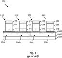
- Fig. 6 schematically illustrates a spin-transfer torque device in the form of a spin-transfer majority gate (STMG) device 600.
- the device 600 includes four magnetic tunnel junction pillars 610, 620, 630, 640, each including a reference layer 612, a pinning layer 614 and a top electrode 616.
- the four pillars 610-640 are as shown arranged on a bottom electrode layer 602, a free layer 604 and a tunnel barrier layer 606, each of which are shared by the four pillars 610-640.
- the pillars 610, 620, 630 form input pillars and the pillar 640 forms an output pillar.
- the magnetization direction of the free layer portion 604d under the output pillar 640 will be influenced by the magnetization of the free layer portions 604a, 604b, 604c under the input pillars 610, 620, 630. More specifically, the magnetization of the free layer portion 604d under the output pillar 640 will assume the direction of the majority of the free layer portions 604a-604c. A majority gate operation is hence realized.
- a spin-transfer torque device typically involves etching through the pinning layer and the reference layer, to form separate pillars with separate pinning and reference layers, while stopping on the tunnel barrier layer. Stopping on the tunnel barrier layer (which may have a thickness on the order of tenths of angstroms) is however challenging, in particular when forming a plurality of pillars in parallel. The etching process may accordingly damage the tunnel barrier layer as well as the underlying free layer. This may cause loss of magnetic anisotropy of the free layer, among others. As a consequence, magnetic and electrical performance may vary across the wafer and causing an overall reduced device performance.
- An objective of the present inventive concept is to provide a spin-transfer torque device, as well as a method for forming such a device, which enables the afore-mentioned issues to be reduced. Further and alternative objectives may be understood from the following.
- a spin-transfer torque device comprising:
- the inventive spin-transfer torque device accordingly includes a coupling layer and a magnetic flux guide layer for coupling of the magnetizations of each one of the separate free layers of the set of magnetic tunnel junction pillars. Free layer-to-free layer interaction is hence provided by means of the coupling layer and the magnetic flux guide layer guiding a magnetic flux between the free layers.
- each magnetic tunnel junction pillar includes a respective separate free layer, a respective separate tunnel barrier layer and a respective separate reference layer, the risk for adversely impacting the device performance during fabrication by unintentional (over-)etching into a common tunnel barrier layer and a common free layer is reduced. Meanwhile, the presence of the coupling layer may protect the magnetic flux guide layer from the etching process. This allows the inventive device to be manufactured at a full wafer scale with magnetic tunnel junction pillars with improved uniformity. Consequently, the coupling layer has a double function of protecting the magnetic flux guide layer during device fabrication and enabling free layer-to-free layer interaction.
- magnetic tunnel junction may be used to refer to the tunnel junction formed by a stack including a reference layer, a tunnel barrier layer and a free layer, which provides the magnetic tunnel function.
- MTJ pillar may be used to refer to the structure including (among others) a MTJ.
- pillar is intended a structure extending in a vertical direction.
- the term “vertical” denotes a geometrical axis being parallel to a stacking direction of the layers of the device.
- a “vertical” axis is perpendicular to a main plane of extension or a main surface of any of the layers of the device, such as the magnetic flux guide layer.
- Terms such as “above” and “under” as used herein may accordingly refer to opposite directions along the vertical axis, with respect to a reference.
- the term “horizontal” denotes a horizontal axis being perpendicular to the vertical axis.
- the device may include a substrate supporting the afore-mentioned layers of the device.
- a "vertical" direction/plane may be understood as a direction/plane being perpendicular to a main plane of extension or main surface of the substrate.
- a “horizontal” direction/plane may be understood as a direction parallel to a main plane of extension or a main surface of the substrate.
- the magnetic flux guide layer (which for brevity may be referred to as the flux guide layer) may, as it is arranged below the magnetic tunnel junction pillars, include a set of portions, each portion being arranged under a respective one of the set of MTJ pillars.
- the flux guide layer may extend uninterrupted between said respective portions to physically connect said respective portions of the flux guide layer.
- a parallel coupling of a magnetization of a free layer to a magnetization of the magnetic flux guide layer through the coupling layer is hereby meant that the magnetization of the free layer is coupled parallel to the magnetization of the magnetic flux guide layer portion under said free layer with such a strength that the magnetizations of said free layer and said magnetic flux guide layer portion are parallel.
- an antiparallel coupling of a magnetization of a free layer to a magnetization of the magnetic flux guide layer through the coupling layer is hereby meant that the magnetization of the free layer is coupled antiparallel to the magnetization of the magnetic flux guide layer portion under said free layer with such a strength that the magnetizations of said free layer and said magnetic flux guide layer portion are antiparallel.
- the magnetic flux guide layer may include a ferromagnetic layer.
- the ferromagnetic layer may be a Co-including layer.
- the Co-including layer may include or consist of Co.
- the magnetic flux guide layer may include a first ferromagnetic layer, a texture breaking layer arranged on the first ferromagnetic layer and a second ferromagnetic layer arranged on the texture breaking layer.
- the first ferromagnetic layer may be a CoFeB-including layer.
- the texture breaking layer may be a Ta-including layer.
- the second ferromagnetic layer may be a Co-including layer. This enables forming of a CoFeB-based flux guide layer with a perpendicular magnetic anisotropy (PMA).
- PMA perpendicular magnetic anisotropy
- the device may further include a seed layer wherein the magnetic flux guide layer is arranged on the seed layer.
- a seed layer may facilitate forming of the flux guide layer with the proper crystal structure and magnetic anisotropy.
- a seed may provide a suitable texture for flux guide layer irrespective of the texture of below layers, such as a bottom electrode layer. It may also contribute to a perpendicular magnetic anisotropy (PMA) of the magnetic flux guide layer via interfacial anisotropy between the seed and the flux guide.
- the seed layer may be an MgO-layer. This enables forming of the aforementioned CoFeB-based flux guide layer with PMA.
- the coupling layer of the spin-transfer torque device may be a non-magnetic layer, adapted to provide a parallel or an antiparallel coupling of magnetizations.
- the coupling layer may, as it is arranged below the magnetic tunnel junction pillars, includes a set of portions, each portion being arranged under a respective one of the set of MTJ pillars.
- the coupling layer may extend uninterrupted between said respective portions to physically connect said respective portions of the coupling layer.
- the separate free layer of a first MTJ pillar of the set of MTJ pillars may be coupled to the flux guide layer portion arranged underneath the first MTJ pillar, via the coupling layer portion arranged underneath the first MTJ pillar.
- the separate free layer of a second MTJ pillar of the set of MTJ pillars may be coupled to the flux guide layer portion arranged underneath the second MTJ pillar, via the coupling layer portion arranged underneath the second MTJ pillar. This may apply correspondingly to any further MTJ pillars of the set of MTJ pillars (e.g. a third MTJ pillar, a fourth MTJ pillar, etc.)
- the coupling layer may be a transition metal-including layer providing an RKKY-coupling oscillating between parallel and antiparallel as a function of layer thickness, wherein the thickness of the transition metal layer is such that the RKKY-coupling is either parallel or antiparallel.
- a transition metal-including layer providing an oscillating RKKY-coupling (or shorter "RKKY-metal") makes it possible to provide a coupling- and etch barrier-function by appropriately selecting the thickness thereof.
- the RKKY coupling is also known as the Ruderman-Kittel-Kasuya-Yosida interaction.
- a coupling layer of a RKKY-metals may provide a favorable etch stopping power to typical dry etching processes.
- the coupling layer may be a Ru-, Ir-, Os-, or Rh- including layer. These materials allow forming of a coupling layer providing a sufficiently strong coupling, a texture compatible with materials typically used in state of the art MTJs and a favorable etch stopping power during MTJ pillar dry etching, for instance by ion beam etching (IBE) or reactive ion etching (RIE).
- IBE ion beam etching
- RIE reactive ion etching
- the coupling layer may be a layer including or consisting of Ru and having a thickness in the range of 13 ⁇ ⁇ 2 ⁇ .
- the coupling layer may be of a sufficient thickness to act as an etch stop and also provide a parallel coupling between the separate free layers and the magnetic flux guide layer, with a strength allowing the respective magnetic flux guide layer portions to exhibit a magnetization parallel to that of the respective separate free layers.
- the coupling layer may be a layer including or consisting of Ru and having a thickness in the range of or 18 ⁇ ⁇ 2 ⁇ .
- the coupling layer may be of a sufficient thickness to act as an etch stop and also provide an antiparallel coupling between the separate free layers and the magnetic flux guide layer, with a strength allowing the respective magnetic flux guide layer portions to exhibit a magnetization opposite to that of the respective separate free layers.
- the coupling layer may be a layer including or consisting of Ir and having a thickness in the range of 14 ⁇ ⁇ 1 ⁇ or in the range of 17 ⁇ ⁇ 2 ⁇ , or in the range of 20 ⁇ ⁇ 2 ⁇ . Thereby, the coupling layer may be of a sufficient thickness to act as an etch stop and provide a parallel or antiparallel coupling, respectively.
- the coupling layer may be a layer including or consisting of Rh and having a thickness in the range of 18 ⁇ ⁇ 2 ⁇ or in the range of 15 ⁇ ⁇ 1 ⁇ . Thereby, the coupling layer may be of a sufficient thickness to act as an etch stop and provide an antiparallel or parallel coupling, respectively.
- Each MTJ pillar of the set of MTJ pillars includes a separate free layer. Accordingly, the free layer of each MTJ pillar is physically disconnected from the free layers of the other MTJ pillars of the set of MTJ pillars.
- Each free layer may include a ferromagnetic layer.
- Each free layer may be a layer having a (net) magnetization which may be varied such that the direction of the magnetization or magnetic moments of the free layer may be varied.
- the direction of the magnetization of the free layer may be switched between two states, a "parallel" state wherein the magnetization direction of the free layer is parallel to the magnetization direction of the reference layer and an "antiparallel” state wherein the magnetization direction of the free layer is antiparallel to the magnetization direction of the reference layer.
- the free layer may also be referred to as a storage layer.
- the magnetization of the free layer may be oriented in-plane (in-plane magnetic anisotropy) or out of plane (perpendicular magnetic anisotropy, PMA).
- the coupling layer may be arranged directly on the flux guide layer and the free layers of the MTJ pillars may be arranged directly on the coupling layer.
- a magnetic coupling strength may be determined mainly by the materials selection of the coupling layer and its thickness without any intermediate layers reducing the coupling strength.
- Each MTJ pillar of the set of MTJ pillars includes a separate tunnel barrier layer. Accordingly, the tunnel barrier layer of each MTJ pillar may be physically disconnected from the tunnel barrier layers of the other MTJ pillars of the set of MTJ pillars.
- Each tunnel barrier layer may be a layer arranged between the reference layer and the free layer.
- the tunnel barrier layer may be adapted to allow a tunneling current across the tunnel barrier layer.
- the tunnel barrier layer may be a non-magnetic and electrically insulating layer.
- Each MTJ pillar of the set of MTJ pillars includes a separate reference layer. Accordingly, the reference layer of each MTJ pillar may be physically disconnected from the reference layers of the other MTJ pillars of the set of MTJ pillars.
- Each reference layer may be a layer having a magnetization which is fixed or pinned. That is, the direction of the magnetization or magnetic moments of the reference layer is fixed or pinned.
- the reference layer may also be referred to as the fixed layer or the pinned layer.
- the magnetization of the reference layer may be oriented in-plane (in-plane magnetic anisotropy) or out of plane (PMA).
- Each reference layer may include a ferromagnetic layer.
- Each reference layer may be a single material layer, or a composite layer formed by a number of sub-layers, at least one of the sub-layers being ferromagnetic.
- a relative orientation of the magnetization directions of the reference layer and the free layer of an MTJ pillar influences an electric resistance of the MTJ pillar.
- the MTJ pillar may exhibit a relatively low resistance when the magnetization of the reference layer and the free layer are aligned or parallel and a relatively high resistance when the magnetisation directions of the reference layer and the free layer are antiparallel with respect to each other.
- the tunnel magnetoresistance ratio (TMR) is a measure of the difference in the MTJ electrical resistance between the antiparallel state and the parallel state.
- Each MTJ pillar of the set of MTJ pillars may further include a separate pinning layer.
- the pinning layer may be arranged above the reference layer.
- Each pinning layer may be adapted to fix or pin the magnetization direction of the reference layer underneath. By the pinning effect exerted on the reference layer by the pinning layer, the reversal field of the reference layer may be increased compared to the reversal field free layer.
- Each pinning layer may include a hard ferromagnetic layer.
- Each pinning layer may also be configured as a synthetic antiferromagnetic layer.
- the spin-transfer torque device may further comprise a bottom electrode layer arranged under the flux guide layer.
- the bottom electrode layer may be electrically connected to each one of the magnetic tunnel junction pillars through the flux guide layer and the coupling layer.
- the spin-transfer torque device may further comprise a separate top electrode arranged on a respective one of the magnetic tunnel junction pillars. Currents (e.g. for reading or writing) may accordingly be selectively applied to each one of the MTJ pillars of the set.
- a respective conductive path may be formed between the bottom electrode layer and each one of the top electrodes of the MTJ pillars.
- the set of MTJ pillars includes at least one magnetic tunnel junction pillar configured as an input pillar and at least one magnetic tunnel junction pillars configured as an output pillar, wherein a magnetization state of the separate free layer of each of said at least one input pillar is configured to influence a magnetization state of the separate free layer of each of said at least one output pillar via the coupling layer and the magnetic flux guide layer.
- the device may hence be configured as a spin-logic device wherein a magnetization state of the free layer of the output pillar is dependent on the magnetization states of the free layers of the input pillars.
- the spin-transfer torque device may be configured as a majority gate device including three input pillars and one output pillar.
- a spin-transfer torque device comprising:
- a magnetization state of the free layer of the output pillar is dependent on the magnetization states of the free layers of the input pillars and may hence be set to either an antiparallel state or a parallel state.
- the spin-transfer torque device is configured as a majority gate device
- the free layer of the output pillar will assume a magnetization state corresponding to that of a majority of the free layers of the input pillars.
- a spin-transfer torque device comprising:
- the coupling layer may cover and thus counteract etching of the flux guide layer.
- a spin-transfer torque device having the advantages described in the above may accordingly be manufactured.
- the etching of the layer stack may be stopped at or on the coupling layer. Accordingly, a number of discrete magnetic tunnel junction pillars may be formed, each extending vertically from the coupling layer.
- the method may further comprise forming a bottom electrode layer and subsequently forming the layer stack above the bottom electrode layer.
- Forming the layer stack may further include forming a top electrode layer, wherein said top electrode layer is formed into separate top electrodes on the plurality of separate magnetic tunnel junction pillars during said etching. Top electrodes may hence be formed in a self-aligned manner with respect to the separate magnetic tunnel junction pillars.
- Figure 1 schematically illustrates cross-sectional side-view of a spin-transfer torque device 100.
- Figure 2 schematically illustrates a top-down view of the device 100.
- the cross-section in figure 1 is taken along the curve AB indicated in figure 2 .
- the device 100 includes a plurality of layers, stacked along a vertical direction denoted Y.
- a main plane of extension of each layer is parallel to a horizontal plane denoted X.
- X horizontal plane
- the spin-transfer torque device 100 comprises a magnetic flux guide layer 104.
- the device 100 comprises a coupling layer 106 arranged on the flux guide layer 104.
- the device 100 comprises a set of magnetic tunnel junction (MTJ) pillars 110, 120, 130, 140.
- the MTJ pillars 110-140 are arranged on the coupling layer 106.
- Each one of the MTJ pillars 110, 120, 130, 140 includes a separate free layer 112, 122, 132, 142, a separate tunnel barrier layer 114, 124, 134, 144 and a separate reference layer 116, 126, 136, 146.
- a magnetization of each one of the separate free layers 112, 122, 132, 142 is coupled to a magnetization of the flux guide layer 104, through the coupling layer 106.
- the illustrated device 100 includes four MTJ pillars 110-140 and is configured as a majority gate device wherein the MTJ pillars 110, 120, 130 are configured as input pillars and the MTJ pillar 140 is configured as an output pillar.
- the device 100 may include further majority gate devices formed by further similarly configured sets of three or more input MTJ pillars and one output MTJ pillar. As shown in figure 2 , the input pillars 110-130 are circumferentially distributed about the output pillar 140. Other arrangements are also possible such as a cross-configuration etc.
- the spin-transfer torque device 100 includes a substrate 101.
- the substrate 101 may be any conventional substrate or wafer, such as a semiconductor substrate.
- semiconductor substrates include a Si substrate, a Ge substrate, a SiGe substrate, a SiC substrate, a SOI substrate, a GeOI substrate, a SiGeOI substrate to name a few.
- the substrate 102 may support an active device portion or front-end-of-line (FEOL) portion including active devices.
- the active devices may be formed in a semiconductor portion of the substrate 101.
- the devices may form logic circuit devices.
- the devices may include switches used for conducting read and write currents for the device 100, as will be described in more detail below.
- Example active devices include MOSFETs, MISFETs, BJTs, JBTs, FinFETs, nanowire FETs to name a few.
- the substrate 101 may further support a not-shown interconnect structure or back-end-of-line (BEOL) portion.
- the BEOL portion may be arranged above the FEOL portion.
- the BEOL-portion may interlayer dielectrics embedding the MTJ pillars 110-140 and a number of metal layers
- the metal layers may be formed by horizontally extending conductive paths.
- Metal layers may for instance be formed by Cu, W, Au, Ag, Al, Co or Ru.
- the interlayer dielectrics may for instance include silicon oxide, silicon oxide nitride, silicon carbide nitride or silicon nitride.
- the BEOL-portion may further include conductive vertical vias interconnecting metal layers through the interlayer dielectrics.
- Vias may for instance be formed by Cu, W, Au, Ag, Al, Co, Ni, Ru or by highly doped semiconductor materials.
- One or more of the metal layers may define bit lines, word lines, select lines or the like for the MTJs.
- the conductive paths of the BEOL-portion may together with the active devices of the FEOL-portion define logic circuitry for controlling reading and writing operations and for driving bit lines, word lines etc.
- the device 100 comprises a bottom electrode layer 102.
- the bottom electrode layer 102 is arranged under the flux guide layer 104.
- the bottom electrode layer 102 may be formed of Ta, Ti, TaN, TiN.
- the bottom electrode layer 102 may also be formed of an alloy, or as a composite layer of sub-layers, of two or more of said materials.
- the bottom electrode layer 102 may be arranged on and in contact with a conductive line or a via of the BEOL-portion.
- the conductive line or via may in turn be connected to a source/drain electrode of a transistor, such as an access transistor.
- the bottom electrode layer 102 need not be common to the MTJ pillars 110-140 but a discrete bottom electrode may be formed under each one of the MTJ pillars 110-140. Each discrete bottom electrode may accordingly be connected to a separate access transistor. Thereby the MTJ pillars 110-140 may be individually addressed.
- the device 100 comprises a seed layer 103.
- the seed layer 103 is arranged on the bottom electrode layer 102.
- the seed layer 103 may be adapted to provide a suitable texture for the flux guide layer 104.
- the seed layer 104 be a single layer, for instance of a metal such as Ta, Ru, Mo, W, Hf, Ni, Cr, Pt, Pd, PtMn or IrMn, or alloys thereof.
- the seed layer 104 may also be an oxide layer such as MgO, MgTiO, or MgAlO.
- the seed layer 103 may also be a composite layer formed by a number of sub-layers.
- the seed layer 103 may for instance be a composite layer of a Ta-layer, a CoFeB-layer and an MgO-layer.
- the thickness of the seed layer 103 or the sub-layers thereof may be on the order of a few to some tens of Angstroms ( ⁇ )
- the flux guide layer 104 is arranged on the seed layer 103. Depending on the choice of materials for the bottom electrode layer 102 and the flux guide layer 104 it may however be possible to omit the seed layer 103 wherein the flux guide layer 104 may be arranged directly on the bottom electrode layer 102.
- the flux guide layer 104 maybe a single layer of a ferromagnetic material, for instance of Co, CoFe, CoFeB, Fe, FeB or CoB.
- the flux guide layer 104 may also be a composite layer formed by a number of sub-layers, at least one of the sub-layers being ferromagnetic.
- the flux guide layer 104 may for instance be a composite layer of a first ferromagnetic CoFeB-layer, a Ta-layer and a second ferromagnetic Co-including layer.
- the second ferromagnetic layer may be a Co-layer, a CoFe-layer or a laminate of Co/Pt, Co/Pd or Co/Ni.
- the thickness of the flux guide layer 104 or the sub-layers thereof may be on the order of a few to some tens of ⁇ .
- the coupling layer 106 of the device 100 is arranged on the flux guide layer 104.
- the coupling layer 106 may be laterally coextensive with the flux guide layer 104.
- the coupling layer 106 is adapted to a magnetic coupling between the magnetic moments of the separate free layers 112, 122, 132, 142 and the flux guide layer 104.
- the coupling layer 106 may be a single layer of a transition metal such as Ru, Ir or Rh.
- the coupling layer 106 may for instance be formed by a Ru-layer with a thickness of 13 ⁇ ⁇ 2 ⁇ or 18 ⁇ ⁇ 2 ⁇ .
- the coupling layer 106 may also be formed by a Ir-layer with a thickness of 14 ⁇ ⁇ 1 ⁇ , 17 ⁇ ⁇ 2 ⁇ , or 20 ⁇ ⁇ 2 ⁇ .
- the coupling layer 106 may also be formed by a Rh-layer with a thickness of 15 ⁇ ⁇ 1 ⁇ , or 18 ⁇ ⁇ 2 ⁇ .
- the coupling layer 106 may also be a composite layer formed by a number of sub-layers of for instance Ru, Ir, Rh, or Os, or by an alloy of two or more of said materials or an alloy predominantly include one of said materials.
- the coupling layer 106 may be formed by a non-magnetic material providing an either parallel or antiparallel coupling, a texture compatible with materials typically used in state of the art MTJs and providing an etch stopping power during MTJ pillar etching.
- Non-magnetic materials include, in addition to non-ferromagnetic materials, materials presenting no or substantially no net magnetization in absence of an external magnetic field, such as para- and diamagnetic materials.
- each MTJ pillar 110-140 includes respective separate free layer, tunnel barrier and reference layers.
- the MTJ pillar 110 includes in a bottom-up-direction a free layer 112, a tunnel barrier layer 114, a reference layer 116, a pinning layer 118 and a top electrode layer 119.
- the MTJ pillar 110 may include further (not shown) layers arranged between the shown layers.
- the MTJ pillar 110 may for instance, as per se is known in the art, include a texture breaking layer between the reference layer 116 and the pinning layer 118, and/or a capping layer between the pinning layer 118 and the top electrode layer 119.
- the free layer 112 is arranged on the coupling layer 106.
- the free layer 112 may be a single layer of a ferromagnetic material, for instance of Fe, Co, FeB, CoB, CoFe and CoFeB.
- the free layer 120 may also be a composite layer formed by a number of sub-layers, at least one of the sub-layers being ferromagnetic.
- the thickness of the free layer 112 or the sub-layers thereof may be on the order of a few to some tens of ⁇ .
- the tunnel barrier layer 114 is arranged on the free layer 112.
- the tunnel barrier layer 114 may be a single layer of an electrically insulating material, for instance a dielectric material such as MgO, AlO x , MgAlO x or MgTiO x .
- the thickness of the tunnel barrier layer 114 may be on the order of about one to a few ⁇ .
- figure 1 shows a single tunnel barrier configuration
- the MTJ pillar 110 also may include a dual-tunnel barrier layer configuration, such as a stack of a first free layer, a first tunnel barrier layer, a second free layer and a second tunnel barrier layer. This configuration may be extended beyond two tunnel barrier layer configurations in a manner which per se is known in the art.
- the reference layer 116 is arranged on the tunnel barrier layer 116.
- the reference layer 116 may be a single layer of a ferromagnetic material, for instance of Fe, Co, FeB, CoB, CoFe and CoFeB.
- the reference layer 116 may also be a composite layer formed by a number of sub-layers, at least one of the sub-layers being ferromagnetic.
- the reference layer 116 may for instance be a composite layer such as a superlattice laminate including layers of two or more of Fe, Co, FeB, CoB, CoFe and CoFeB.
- the pinning layer 118 is arranged on the reference layer 116.
- the pinning layer 118 may include one or more hard magnetic layers.
- the pinning layer 118 may for instance include a superlattice laminate of a repetitive sequence of [Co/Pd], [Co/Pt] or [Co/Ni] bilayers.
- the pinning layer 118 may also include a Co-layer, an Fe-layer or a CoFe-layer or a superlattice laminate of a repetitive sequence of [Fe/X] or [CoFe/X], where X denotes Pd, Pt, Ni, Tb or Gd.
- the pinning layer 118 may also include an alloy composition, such as an alloy of Co, Fe or CoFe and Pt, Pd, Ni, Tb or Gd, or a ternary alloy of CoXCr, where X denotes Pt, Ni, Pd, Tb or Gd.
- the pinning layer 118 may be anti-ferromagnetically coupled to the reference layer 116 via a non-magnetic spacer layer (not shown), such as a thin Ru-layer.
- the pinning layer 118 may also be also be formed as a synthetic antiferromagnet (SAF) including two hard magnetic layers (e.g. each of a composition as set out above) and separated by a thin non-magnetic spacer layer, such as a Ru or Ir layer.
- a transition layer such a Ta, W, Mo, or alloy thereof or CoX, FeX CoFeX, with X Ta, W, Mo may be present between the reference layer and the pinning layer.
- the top electrode layer 119 is arranged on the pinning layer 118.
- the top electrode layer 119 may be a single layer of for instance Ru or Ta.
- the top electrode layer 119 may also be a composite layer formed by a number of sub-layers, or an alloy, of Ru or Ta.
- the top electrode layer 119 may further be arranged in contact with a conductive line or a via of the BEOL-portion.
- the conductive line or via may in turn be connected to a source/drain electrode of a transistor, such as an access transistor.
- the above description of the MTJ pillar 110 applies correspondingly to the further MTJ pillars 120, 130, 140, each including corresponding free layers 122, 132, 142, tunnel barrier layers 124, 134, 144, reference layers 126, 136, 146, pinning layers 128, 138, 149 and top electrode layers 129, 139, 149.
- a respective conductive path is formed between the bottom electrode layer 100 and each top electrode 119, 129, 139, 149.
- the flux guide layer 104 includes a portion 104a which is arranged under the MTJ pillar 110.
- the flux guide layer 104 further includes portions 104b, 104c and 104d arranged under the MTJ pillar 120, 130 and 140, respectively.
- the flux guide layer 104 extends between and joins the layer portions 104a-d to form a continuous layer.
- the coupling layer 106 includes a coupling layer portion 106a which is arranged under the MTJ pillar 110.
- the coupling layer 106 further includes portions 106b, 106c and 106d arranged under the MTJ pillars 120, 130 and 140, respectively.
- the coupling layer 106 extends between and joins the layer portions 106a-d to form a continuous layer.
- Figure 1 includes arrows representing the direction of magnetization, i.e. the orientation of the magnetic moment, for the various magnetic layers of the device 100.
- figure 1 indicates magnetic layers having perpendicular magnetic anisotropy (PMA), it is as is known to the person skilled in the art also possible to form magnetic layers presenting an in-plane magnetic anisotropy.
- PMA perpendicular magnetic anisotropy
- the magnetization direction of the free layers may be independently switched between two opposite directions, a parallel direction (P) and an antiparallel direction (AP) with respect to the fixed magnetization direction of the respective reference layer 116, 126, 136, 146.
- An arrow indication of the magnetization of the pinning layers 118, 128, 138, 148 has been omitted since, as mentioned above, either SAF- or ferromagnetic configurations are possible.
- the illustrated downward orientation of the magnetization directions of the reference layers 116, 126, 136, 146 is merely an example and an upward orientation may also be established during fabrication.
- the magnetization of the flux guide layer portions 104a-d is coupled antiparallel to the magnetization of the free layers 112, 122, 132, 142, respectively. More specifically, the flux guide layer portion 104a is coupled antiparallel, through the coupling layer portion 106a, to the free layer 112. Correspondingly, each one of the further flux guide layer portions 104b-d is coupled antiparallel, through the respective intermediate coupling layer portion 106-b-d, to the respective free layer 122, 132, 142.
- each flux guide layer portion 104a-d will be antiparallel to the direction of the magnetization of the free layer 112, 122, 132, 142 above.
- the coupling layer 106 may also be formed such that a parallel coupling between the respective free layers 112, 122, 132, 142 and the respective flux guide layer portions 104a-d is provided.
- Figure 3 illustrates the device 100 during operation.
- Write currents I STT1- I STT3 are supplied to the respective input pillars 110-130 in order to set the free layer 112 to a P-state and each of the free layers 122 and 132 to an AP-state.
- the magnetization states of the free layers influence, through the antiparallel coupling through the coupling layer 106, the magnetization state of the respective flux guide layer portions 104a, 104b, 104c.
- the magnetization states of the flux guide layer portions 104a, 104b, 104c may in turn influence the magnetization states of the flux guide layer portion 104d such that the flux guide layer portion 104d assumes the magnetization state of the majority of the flux guide layer portions 104a-c.
- the flux guide layer portion 104d assumes the same magnetization state as the flux guide layer portions 104b,104c.
- the magnetization state of the flux guide layer portions 104d in response influence, through the antiparallel coupling through the coupling layer 106, the magnetization state of the free layer 142.
- Figure 4 illustrates a further operation example wherein write currents instead are supplied to the input pillars 110-130 in order to set the free layer 112 to an AP-state and each of the free layers 122 and 132 to a P-state. In response, the free layer 142 assumes a P-state.
- the state of the free layer 142 may be determined in a same manner as read-out of MTJs of conventional STT-MRAMs. For instance the resistance of the output pillar 140 may be measured after applying a voltage across the output pillar 140. An AP-state (as in figure 3 ) may result in a greater resistance than a P-state (as in figure 4 ). The magnitude of the difference in resistance between a P-state and an AP-state depends on the TMR of the MTJ pillar.
- the device 100 performs a function of a majority gate device.
- a spin-transfer torque device such as the device 100, may be formed by forming a layer stack including a bottom electrode layer 102, a seed layer 103, a magnetic flux guide layer 104, a coupling layer 106, a free layer 1002, a tunnel barrier layer 1004, a reference layer 1006, a pinning layer 1008 and a top electrode layer 1009.
- the layers of the layer stack may be deposited in a manner which per se is known in the art, for instance by a respective sputtering or evaporation process.
- the fabrication process may further include one or more annealing steps for causing crystallization of the magnetic layers while applying a magnetic field to the structure for setting a desired magnetization.
- the bottom electrode layer 102 may following deposition be patterned into a number of discrete bottom electrodes parts with positions corresponding to the intended positions of the MTJ pillars 110-140 which are to be formed.
- a plurality of separate MTJ pillars 110-140 may be formed on the coupling layer 106 by etching the layer stack.
- An anisotropic dry etch process may be used, for instance an ion beam etch (IBE) or reactive ion etch (RIE) process.
- a mask layer (not shown), for instance of a hard mask material such as TiN, Ta or TaN, may be deposited on the top electrode layer 1009 and patterned to form mask portions 1010, 1020, 1030, 1040 defining the positions and cross-sectional dimensions (for instance as oval or circular, or rectangular or more generally polygonal cross sections) of the MTJ pillars 110-140 which are to be formed.
- the pattern defined by the mask portions may subsequently be transferred into the layer stack by etching to form the MTJ pillars 110-140, each pillar including a separate a free layer, a separate tunnel barrier layer, a separate reference layer, a separate pinning layer and a separate top electrode layer.
- the coupling layer 106 may cover and thus counteract etching of the flux guide layer 104.
- the etching of the layer stack may accordingly be stopped on the coupling layer 106, i.e. when the coupling layer 106 is exposed.
- the mask portions 1010-1040 may subsequently be removed.
- a device may include a single input MTJ pillar (such as MTJ pillar 130) and a single output MTJ pillar (such as MTJ pillar 140) arranged on a common flux guide layer and a common coupling layer.
- MTJ pillar 130 a single input MTJ pillar
- output MTJ pillar such as MTJ pillar 140
- the state of the of the output pillar may be controlled by switching the state of the input pillar.
- a spin-logic device may include a set of MTJ pillars formed by at least one MTJ pillar configured as an input pillar and at least one MTJ pillar configured as an output pillar, wherein a magnetization state of the free layer of the output pillar is dependent on the magnetization states of the free layers of the input pillars.
Landscapes
- Engineering & Computer Science (AREA)
- Physics & Mathematics (AREA)
- Computer Hardware Design (AREA)
- Computing Systems (AREA)
- General Engineering & Computer Science (AREA)
- Mathematical Physics (AREA)
- Manufacturing & Machinery (AREA)
- Mram Or Spin Memory Techniques (AREA)
- Hall/Mr Elements (AREA)
Abstract
Description
- The present inventive concept relates to a spin transfer torque device, a method of operating a spin-transfer torque device and a method for forming a spin-transfer torque device.
- A magnetic tunnel junction structure may include a free layer, a tunnel barrier layer, a reference layer and a pinning layer. A magnetization state of the reference layer is fixed or pinned by the pinning layer. A magnetization state of the free layer may be switched between two different directions, parallel and antiparallel to the magnetization direction of the reference layer, by passing a current through the reference layer. The reference layer may spin-polarize the current wherein the spin-polarized current through spin-transfer torque may cause the magnetization state of the free layer to change.
-
Fig. 6 schematically illustrates a spin-transfer torque device in the form of a spin-transfer majority gate (STMG)device 600. Thedevice 600 includes four magnetictunnel junction pillars reference layer 612, apinning layer 614 and atop electrode 616. The four pillars 610-640 are as shown arranged on abottom electrode layer 602, afree layer 604 and atunnel barrier layer 606, each of which are shared by the four pillars 610-640. Thepillars pillar 640 forms an output pillar. As thefree layer 604 is common to the pillars 610-640 the magnetization direction of thefree layer portion 604d under theoutput pillar 640 will be influenced by the magnetization of thefree layer portions input pillars free layer portion 604d under theoutput pillar 640 will assume the direction of the majority of thefree layer portions 604a-604c. A majority gate operation is hence realized. - The inventors have realized that the design of prior art prior art spin-transfer torque devices, such as prior art STMG devices, may be challenging to realize in full wafer scale production. Fabrication of a spin-transfer torque device typically involves etching through the pinning layer and the reference layer, to form separate pillars with separate pinning and reference layers, while stopping on the tunnel barrier layer. Stopping on the tunnel barrier layer (which may have a thickness on the order of tenths of angstroms) is however challenging, in particular when forming a plurality of pillars in parallel. The etching process may accordingly damage the tunnel barrier layer as well as the underlying free layer. This may cause loss of magnetic anisotropy of the free layer, among others. As a consequence, magnetic and electrical performance may vary across the wafer and causing an overall reduced device performance.
- An objective of the present inventive concept is to provide a spin-transfer torque device, as well as a method for forming such a device, which enables the afore-mentioned issues to be reduced. Further and alternative objectives may be understood from the following.
- According to a first aspect of the present inventive concept there is provided a spin-transfer torque device, comprising:
- a magnetic flux guide layer,
- a set of magnetic tunnel junction pillars arranged above the magnetic flux guide layer, wherein each one of said pillars includes a separate free layer, a separate tunnel barrier layer and a separate reference layer, and
- a coupling layer arranged between the magnetic flux guide layer and said magnetic tunnel junction pillars, wherein a magnetization of each one of said separate free layers is coupled parallel or antiparallel to a magnetization of the magnetic flux guide layer, through the coupling layer.
- The inventive spin-transfer torque device accordingly includes a coupling layer and a magnetic flux guide layer for coupling of the magnetizations of each one of the separate free layers of the set of magnetic tunnel junction pillars. Free layer-to-free layer interaction is hence provided by means of the coupling layer and the magnetic flux guide layer guiding a magnetic flux between the free layers.
- Since each magnetic tunnel junction pillar includes a respective separate free layer, a respective separate tunnel barrier layer and a respective separate reference layer, the risk for adversely impacting the device performance during fabrication by unintentional (over-)etching into a common tunnel barrier layer and a common free layer is reduced. Meanwhile, the presence of the coupling layer may protect the magnetic flux guide layer from the etching process. This allows the inventive device to be manufactured at a full wafer scale with magnetic tunnel junction pillars with improved uniformity. Consequently, the coupling layer has a double function of protecting the magnetic flux guide layer during device fabrication and enabling free layer-to-free layer interaction.
- In the following, the terminology magnetic tunnel junction (MTJ) may be used to refer to the tunnel junction formed by a stack including a reference layer, a tunnel barrier layer and a free layer, which provides the magnetic tunnel function. Meanwhile, the terminology MTJ pillar may be used to refer to the structure including (among others) a MTJ.
- By pillar is intended a structure extending in a vertical direction.
- As used herein, the term "vertical" (for instance with reference to a direction or a plane) denotes a geometrical axis being parallel to a stacking direction of the layers of the device. Correspondingly, a "vertical" axis is perpendicular to a main plane of extension or a main surface of any of the layers of the device, such as the magnetic flux guide layer. Terms such as "above" and "under" as used herein may accordingly refer to opposite directions along the vertical axis, with respect to a reference. As used herein, the term "horizontal" denotes a horizontal axis being perpendicular to the vertical axis.
- The device may include a substrate supporting the afore-mentioned layers of the device. In this case, a "vertical" direction/plane may be understood as a direction/plane being perpendicular to a main plane of extension or main surface of the substrate. Correspondingly a "horizontal" direction/plane may be understood as a direction parallel to a main plane of extension or a main surface of the substrate.
- The magnetic flux guide layer (which for brevity may be referred to as the flux guide layer) may, as it is arranged below the magnetic tunnel junction pillars, include a set of portions, each portion being arranged under a respective one of the set of MTJ pillars. The flux guide layer may extend uninterrupted between said respective portions to physically connect said respective portions of the flux guide layer.
- By a parallel coupling of a magnetization of a free layer to a magnetization of the magnetic flux guide layer through the coupling layer is hereby meant that the magnetization of the free layer is coupled parallel to the magnetization of the magnetic flux guide layer portion under said free layer with such a strength that the magnetizations of said free layer and said magnetic flux guide layer portion are parallel.
- By an antiparallel coupling of a magnetization of a free layer to a magnetization of the magnetic flux guide layer through the coupling layer is hereby meant that the magnetization of the free layer is coupled antiparallel to the magnetization of the magnetic flux guide layer portion under said free layer with such a strength that the magnetizations of said free layer and said magnetic flux guide layer portion are antiparallel.
- The magnetic flux guide layer may include a ferromagnetic layer. The ferromagnetic layer may be a Co-including layer. The Co-including layer may include or consist of Co. The magnetic flux guide layer may include a first ferromagnetic layer, a texture breaking layer arranged on the first ferromagnetic layer and a second ferromagnetic layer arranged on the texture breaking layer. The first ferromagnetic layer may be a CoFeB-including layer. The texture breaking layer may be a Ta-including layer. The second ferromagnetic layer may be a Co-including layer. This enables forming of a CoFeB-based flux guide layer with a perpendicular magnetic anisotropy (PMA).
- The device may further include a seed layer wherein the magnetic flux guide layer is arranged on the seed layer. A seed layer may facilitate forming of the flux guide layer with the proper crystal structure and magnetic anisotropy. In particular, a seed may provide a suitable texture for flux guide layer irrespective of the texture of below layers, such as a bottom electrode layer. It may also contribute to a perpendicular magnetic anisotropy (PMA) of the magnetic flux guide layer via interfacial anisotropy between the seed and the flux guide. The seed layer may be an MgO-layer. This enables forming of the aforementioned CoFeB-based flux guide layer with PMA.
- The coupling layer of the spin-transfer torque device may be a non-magnetic layer, adapted to provide a parallel or an antiparallel coupling of magnetizations.
- The coupling layer may, as it is arranged below the magnetic tunnel junction pillars, includes a set of portions, each portion being arranged under a respective one of the set of MTJ pillars. The coupling layer may extend uninterrupted between said respective portions to physically connect said respective portions of the coupling layer.
- Accordingly, the separate free layer of a first MTJ pillar of the set of MTJ pillars may be coupled to the flux guide layer portion arranged underneath the first MTJ pillar, via the coupling layer portion arranged underneath the first MTJ pillar. The separate free layer of a second MTJ pillar of the set of MTJ pillars may be coupled to the flux guide layer portion arranged underneath the second MTJ pillar, via the coupling layer portion arranged underneath the second MTJ pillar. This may apply correspondingly to any further MTJ pillars of the set of MTJ pillars (e.g. a third MTJ pillar, a fourth MTJ pillar, etc.)
- The coupling layer may be a transition metal-including layer providing an RKKY-coupling oscillating between parallel and antiparallel as a function of layer thickness, wherein the thickness of the transition metal layer is such that the RKKY-coupling is either parallel or antiparallel. A transition metal-including layer providing an oscillating RKKY-coupling (or shorter "RKKY-metal") makes it possible to provide a coupling- and etch barrier-function by appropriately selecting the thickness thereof. The RKKY coupling is also known as the Ruderman-Kittel-Kasuya-Yosida interaction. A coupling layer of a RKKY-metals may provide a favorable etch stopping power to typical dry etching processes.
- The coupling layer may be a Ru-, Ir-, Os-, or Rh- including layer. These materials allow forming of a coupling layer providing a sufficiently strong coupling, a texture compatible with materials typically used in state of the art MTJs and a favorable etch stopping power during MTJ pillar dry etching, for instance by ion beam etching (IBE) or reactive ion etching (RIE).
- The coupling layer may be a layer including or consisting of Ru and having a thickness in the range of 13 Å ±2 Å. Thereby, the coupling layer may be of a sufficient thickness to act as an etch stop and also provide a parallel coupling between the separate free layers and the magnetic flux guide layer, with a strength allowing the respective magnetic flux guide layer portions to exhibit a magnetization parallel to that of the respective separate free layers. Alternatively, the coupling layer may be a layer including or consisting of Ru and having a thickness in the range of or 18 Å ±2 Å. Thereby, the coupling layer may be of a sufficient thickness to act as an etch stop and also provide an antiparallel coupling between the separate free layers and the magnetic flux guide layer, with a strength allowing the respective magnetic flux guide layer portions to exhibit a magnetization opposite to that of the respective separate free layers.
- The coupling layer may be a layer including or consisting of Ir and having a thickness in the range of 14 Å ±1 Å or in the range of 17 Å ± 2 Å, or in the range of 20 Å ± 2Å. Thereby, the coupling layer may be of a sufficient thickness to act as an etch stop and provide a parallel or antiparallel coupling, respectively.
- The coupling layer may be a layer including or consisting of Rh and having a thickness in the range of 18 Å ±2 Å or in the range of 15 Å ± 1 Å. Thereby, the coupling layer may be of a sufficient thickness to act as an etch stop and provide an antiparallel or parallel coupling, respectively.
- Each MTJ pillar of the set of MTJ pillars includes a separate free layer. Accordingly, the free layer of each MTJ pillar is physically disconnected from the free layers of the other MTJ pillars of the set of MTJ pillars.
- Each free layer may include a ferromagnetic layer. Each free layer may be a layer having a (net) magnetization which may be varied such that the direction of the magnetization or magnetic moments of the free layer may be varied. The direction of the magnetization of the free layer may be switched between two states, a "parallel" state wherein the magnetization direction of the free layer is parallel to the magnetization direction of the reference layer and an "antiparallel" state wherein the magnetization direction of the free layer is antiparallel to the magnetization direction of the reference layer. The free layer may also be referred to as a storage layer. The magnetization of the free layer may be oriented in-plane (in-plane magnetic anisotropy) or out of plane (perpendicular magnetic anisotropy, PMA).
- The coupling layer may be arranged directly on the flux guide layer and the free layers of the MTJ pillars may be arranged directly on the coupling layer. Thereby a magnetic coupling strength may be determined mainly by the materials selection of the coupling layer and its thickness without any intermediate layers reducing the coupling strength.
- Each MTJ pillar of the set of MTJ pillars includes a separate tunnel barrier layer. Accordingly, the tunnel barrier layer of each MTJ pillar may be physically disconnected from the tunnel barrier layers of the other MTJ pillars of the set of MTJ pillars.
- Each tunnel barrier layer may be a layer arranged between the reference layer and the free layer. The tunnel barrier layer may be adapted to allow a tunneling current across the tunnel barrier layer. The tunnel barrier layer may be a non-magnetic and electrically insulating layer.
- Each MTJ pillar of the set of MTJ pillars includes a separate reference layer. Accordingly, the reference layer of each MTJ pillar may be physically disconnected from the reference layers of the other MTJ pillars of the set of MTJ pillars.
- Each reference layer may be a layer having a magnetization which is fixed or pinned. That is, the direction of the magnetization or magnetic moments of the reference layer is fixed or pinned. The reference layer may also be referred to as the fixed layer or the pinned layer. The magnetization of the reference layer may be oriented in-plane (in-plane magnetic anisotropy) or out of plane (PMA).
- Each reference layer may include a ferromagnetic layer. Each reference layer may be a single material layer, or a composite layer formed by a number of sub-layers, at least one of the sub-layers being ferromagnetic.
- A relative orientation of the magnetization directions of the reference layer and the free layer of an MTJ pillar influences an electric resistance of the MTJ pillar. The MTJ pillar may exhibit a relatively low resistance when the magnetization of the reference layer and the free layer are aligned or parallel and a relatively high resistance when the magnetisation directions of the reference layer and the free layer are antiparallel with respect to each other. The tunnel magnetoresistance ratio (TMR) is a measure of the difference in the MTJ electrical resistance between the antiparallel state and the parallel state.
- Each MTJ pillar of the set of MTJ pillars may further include a separate pinning layer. The pinning layer may be arranged above the reference layer. Each pinning layer may be adapted to fix or pin the magnetization direction of the reference layer underneath. By the pinning effect exerted on the reference layer by the pinning layer, the reversal field of the reference layer may be increased compared to the reversal field free layer.
- Each pinning layer may include a hard ferromagnetic layer. Each pinning layer may also be configured as a synthetic antiferromagnetic layer.
- The spin-transfer torque device may further comprise a bottom electrode layer arranged under the flux guide layer. The bottom electrode layer may be electrically connected to each one of the magnetic tunnel junction pillars through the flux guide layer and the coupling layer. By providing a common bottom electrode layer, the need for plural electrical interconnections to the bottom part of the device may be avoided.
- The spin-transfer torque device may further comprise a separate top electrode arranged on a respective one of the magnetic tunnel junction pillars. Currents (e.g. for reading or writing) may accordingly be selectively applied to each one of the MTJ pillars of the set.
- In combination with a common bottom electrode layer, a respective conductive path may be formed between the bottom electrode layer and each one of the top electrodes of the MTJ pillars.
- According to one embodiment the set of MTJ pillars includes at least one magnetic tunnel junction pillar configured as an input pillar and at least one magnetic tunnel junction pillars configured as an output pillar, wherein a magnetization state of the separate free layer of each of said at least one input pillar is configured to influence a magnetization state of the separate free layer of each of said at least one output pillar via the coupling layer and the magnetic flux guide layer. The device may hence be configured as a spin-logic device wherein a magnetization state of the free layer of the output pillar is dependent on the magnetization states of the free layers of the input pillars.
- The spin-transfer torque device may be configured as a majority gate device including three input pillars and one output pillar.
- According to a second aspect of the present inventive concept, there is provided a method of operating a spin-transfer torque device, the method comprising:
- applying a write current to a number of said input pillars to set a magnetization state of the separate free layer of each of said input pillars (e.g. to an antiparallel state or a parallel state), thereby influencing a magnetization state of the separate free layer of the output pillar, and
- determining a magnetization state of the separate free layer of the output pillar.
- Since the respective magnetization of the separate free layers of the input pillars are coupled to the magnetization of the free layer of the output pillar via the coupling layer and the magnetic flux guide layer, a magnetization state of the free layer of the output pillar is dependent on the magnetization states of the free layers of the input pillars and may hence be set to either an antiparallel state or a parallel state. By applying a write current to a number of the input pillars and determining a resulting magnetization state of the separate free layer of the output pillar, an input-output characteristic of the device may be determined.
- In case the spin-transfer torque device is configured as a majority gate device, the free layer of the output pillar will assume a magnetization state corresponding to that of a majority of the free layers of the input pillars.
- According to a third aspect of the present inventive concept, there is provided a method for forming a spin-transfer torque device, the method comprising:
- forming a layer stack including: a magnetic flux guide layer, a coupling layer, a free layer, a tunnel barrier layer and a reference layer, and
- forming, by etching the layer stack, a plurality of separate magnetic tunnel junction pillars above the coupling layer, each magnetic tunnel junction pillar including a separate a free layer, a separate tunnel barrier layer and a separate reference layer, wherein the separate free layer of each one of the plurality of magnetic tunnel junction pillars is coupled parallel or antiparallel to the magnetic flux guide layer, through the coupling layer.
- During the etching of the layer stack, the coupling layer may cover and thus counteract etching of the flux guide layer. A spin-transfer torque device having the advantages described in the above may accordingly be manufactured.
- The etching of the layer stack may be stopped at or on the coupling layer. Accordingly, a number of discrete magnetic tunnel junction pillars may be formed, each extending vertically from the coupling layer.
- The method may further comprise forming a bottom electrode layer and subsequently forming the layer stack above the bottom electrode layer.
- Forming the layer stack may further include forming a top electrode layer, wherein said top electrode layer is formed into separate top electrodes on the plurality of separate magnetic tunnel junction pillars during said etching. Top electrodes may hence be formed in a self-aligned manner with respect to the separate magnetic tunnel junction pillars.
- The above, as well as additional objects, features and advantages of the present inventive concept, will be better understood through the following illustrative and non-limiting detailed description, with reference to the appended drawings. In the drawings like reference numerals will be used for like elements unless stated otherwise.
-
Fig. 1 is a schematic side-view of a spin-transfer torque device. -
Fig. 2 is a schematic top-view of a spin-transfer torque device. -
Fig. 3 and 4 illustrate a spin-transfer torque device during operation. -
Fig. 5a-b illustrates a method for forming a spin-transfer torque device. -
Fig. 6 illustrates a prior art spin-transfer torque device. -
Figure 1 schematically illustrates cross-sectional side-view of a spin-transfer torque device 100.Figure 2 schematically illustrates a top-down view of thedevice 100. To facilitate understanding of the structure of thedevice 100, the cross-section infigure 1 is taken along the curve AB indicated infigure 2 . As shown, thedevice 100 includes a plurality of layers, stacked along a vertical direction denoted Y. A main plane of extension of each layer is parallel to a horizontal plane denoted X. It should be noted that for the purpose of illustrational clarity the various layers and other features of the stacks are not drawn to scale and their relative dimensions, in particular their thickness, may differ from a physical stack. - The spin-
transfer torque device 100 comprises a magneticflux guide layer 104. Thedevice 100 comprises acoupling layer 106 arranged on theflux guide layer 104. Thedevice 100 comprises a set of magnetic tunnel junction (MTJ)pillars coupling layer 106. Each one of theMTJ pillars free layer tunnel barrier layer separate reference layer free layers flux guide layer 104, through thecoupling layer 106. - The illustrated
device 100 includes four MTJ pillars 110-140 and is configured as a majority gate device wherein theMTJ pillars MTJ pillar 140 is configured as an output pillar. Thedevice 100 may include further majority gate devices formed by further similarly configured sets of three or more input MTJ pillars and one output MTJ pillar. As shown infigure 2 , the input pillars 110-130 are circumferentially distributed about theoutput pillar 140. Other arrangements are also possible such as a cross-configuration etc. - The spin-
transfer torque device 100 includes asubstrate 101. Thesubstrate 101 may be any conventional substrate or wafer, such as a semiconductor substrate. Examples of semiconductor substrates include a Si substrate, a Ge substrate, a SiGe substrate, a SiC substrate, a SOI substrate, a GeOI substrate, a SiGeOI substrate to name a few. - Although not shown in
figure 1 , thesubstrate 102 may support an active device portion or front-end-of-line (FEOL) portion including active devices. The active devices may be formed in a semiconductor portion of thesubstrate 101. The devices may form logic circuit devices. The devices may include switches used for conducting read and write currents for thedevice 100, as will be described in more detail below. Example active devices include MOSFETs, MISFETs, BJTs, JBTs, FinFETs, nanowire FETs to name a few. - The
substrate 101 may further support a not-shown interconnect structure or back-end-of-line (BEOL) portion. The BEOL portion may be arranged above the FEOL portion. The BEOL-portion may interlayer dielectrics embedding the MTJ pillars 110-140 and a number of metal layers The metal layers may be formed by horizontally extending conductive paths. Metal layers may for instance be formed by Cu, W, Au, Ag, Al, Co or Ru. The interlayer dielectrics may for instance include silicon oxide, silicon oxide nitride, silicon carbide nitride or silicon nitride. The BEOL-portion may further include conductive vertical vias interconnecting metal layers through the interlayer dielectrics. Vias may for instance be formed by Cu, W, Au, Ag, Al, Co, Ni, Ru or by highly doped semiconductor materials. One or more of the metal layers may define bit lines, word lines, select lines or the like for the MTJs. The conductive paths of the BEOL-portion may together with the active devices of the FEOL-portion define logic circuitry for controlling reading and writing operations and for driving bit lines, word lines etc. - The
device 100 comprises abottom electrode layer 102. Thebottom electrode layer 102 is arranged under theflux guide layer 104. Thebottom electrode layer 102 may be formed of Ta, Ti, TaN, TiN. Thebottom electrode layer 102 may also be formed of an alloy, or as a composite layer of sub-layers, of two or more of said materials. Thebottom electrode layer 102 may be arranged on and in contact with a conductive line or a via of the BEOL-portion. The conductive line or via may in turn be connected to a source/drain electrode of a transistor, such as an access transistor. - According to a variation, the
bottom electrode layer 102 need not be common to the MTJ pillars 110-140 but a discrete bottom electrode may be formed under each one of the MTJ pillars 110-140. Each discrete bottom electrode may accordingly be connected to a separate access transistor. Thereby the MTJ pillars 110-140 may be individually addressed. - The
device 100 comprises aseed layer 103. Theseed layer 103 is arranged on thebottom electrode layer 102. Theseed layer 103 may be adapted to provide a suitable texture for theflux guide layer 104. Theseed layer 104 be a single layer, for instance of a metal such as Ta, Ru, Mo, W, Hf, Ni, Cr, Pt, Pd, PtMn or IrMn, or alloys thereof. Theseed layer 104 may also be an oxide layer such as MgO, MgTiO, or MgAlO. Theseed layer 103 may also be a composite layer formed by a number of sub-layers. Theseed layer 103 may for instance be a composite layer of a Ta-layer, a CoFeB-layer and an MgO-layer. The thickness of theseed layer 103 or the sub-layers thereof may be on the order of a few to some tens of Angstroms (Å) - The
flux guide layer 104 is arranged on theseed layer 103. Depending on the choice of materials for thebottom electrode layer 102 and theflux guide layer 104 it may however be possible to omit theseed layer 103 wherein theflux guide layer 104 may be arranged directly on thebottom electrode layer 102. Theflux guide layer 104 maybe a single layer of a ferromagnetic material, for instance of Co, CoFe, CoFeB, Fe, FeB or CoB. Theflux guide layer 104 may also be a composite layer formed by a number of sub-layers, at least one of the sub-layers being ferromagnetic. Theflux guide layer 104 may for instance be a composite layer of a first ferromagnetic CoFeB-layer, a Ta-layer and a second ferromagnetic Co-including layer. The second ferromagnetic layer may be a Co-layer, a CoFe-layer or a laminate of Co/Pt, Co/Pd or Co/Ni. The thickness of theflux guide layer 104 or the sub-layers thereof may be on the order of a few to some tens of Å. - The
coupling layer 106 of thedevice 100 is arranged on theflux guide layer 104. Thecoupling layer 106 may be laterally coextensive with theflux guide layer 104. Thecoupling layer 106 is adapted to a magnetic coupling between the magnetic moments of the separatefree layers flux guide layer 104. Thecoupling layer 106 may be a single layer of a transition metal such as Ru, Ir or Rh. Thecoupling layer 106 may for instance be formed by a Ru-layer with a thickness of 13 Å ±2 Å or 18 Å ±2 Å. Thecoupling layer 106 may also be formed by a Ir-layer with a thickness of 14 Å ±1 Å, 17 Å ± 2 Å, or 20 Å ± 2Å. Thecoupling layer 106 may also be formed by a Rh-layer with a thickness of 15 Å ±1 Å, or 18 Å ± 2Å. Thecoupling layer 106 may also be a composite layer formed by a number of sub-layers of for instance Ru, Ir, Rh, or Os, or by an alloy of two or more of said materials or an alloy predominantly include one of said materials. More generally thecoupling layer 106 may be formed by a non-magnetic material providing an either parallel or antiparallel coupling, a texture compatible with materials typically used in state of the art MTJs and providing an etch stopping power during MTJ pillar etching. Non-magnetic materials include, in addition to non-ferromagnetic materials, materials presenting no or substantially no net magnetization in absence of an external magnetic field, such as para- and diamagnetic materials. - As described above, each MTJ pillar 110-140 includes respective separate free layer, tunnel barrier and reference layers. The
MTJ pillar 110 includes in a bottom-up-direction afree layer 112, atunnel barrier layer 114, areference layer 116, a pinninglayer 118 and atop electrode layer 119. TheMTJ pillar 110 may include further (not shown) layers arranged between the shown layers. TheMTJ pillar 110 may for instance, as per se is known in the art, include a texture breaking layer between thereference layer 116 and the pinninglayer 118, and/or a capping layer between the pinninglayer 118 and thetop electrode layer 119. - The
free layer 112 is arranged on thecoupling layer 106. Thefree layer 112 may be a single layer of a ferromagnetic material, for instance of Fe, Co, FeB, CoB, CoFe and CoFeB. Thefree layer 120 may also be a composite layer formed by a number of sub-layers, at least one of the sub-layers being ferromagnetic. Thefree layer 112 may for instance be a composite layer such as a Co/X/CoFeB tri-layer where X denotes for instance Ta, W or Mo, V, Hf, Cr and alloys thereof and CoFeX, CoFeBX, FeBX, CoBX with X= Ta, W, Mo, V, Cr, Hf or combinations thereof. The thickness of thefree layer 112 or the sub-layers thereof may be on the order of a few to some tens of Å. - The
tunnel barrier layer 114 is arranged on thefree layer 112. Thetunnel barrier layer 114 may be a single layer of an electrically insulating material, for instance a dielectric material such as MgO, AlOx, MgAlOx or MgTiOx. The thickness of thetunnel barrier layer 114 may be on the order of about one to a few Å. Althoughfigure 1 shows a single tunnel barrier configuration, theMTJ pillar 110 also may include a dual-tunnel barrier layer configuration, such as a stack of a first free layer, a first tunnel barrier layer, a second free layer and a second tunnel barrier layer. This configuration may be extended beyond two tunnel barrier layer configurations in a manner which per se is known in the art. - The
reference layer 116 is arranged on thetunnel barrier layer 116. Thereference layer 116 may be a single layer of a ferromagnetic material, for instance of Fe, Co, FeB, CoB, CoFe and CoFeB. Thereference layer 116 may also be a composite layer formed by a number of sub-layers, at least one of the sub-layers being ferromagnetic. Thereference layer 116 may for instance be a composite layer such as a superlattice laminate including layers of two or more of Fe, Co, FeB, CoB, CoFe and CoFeB. - The pinning
layer 118 is arranged on thereference layer 116. The pinninglayer 118 may include one or more hard magnetic layers. The pinninglayer 118 may for instance include a superlattice laminate of a repetitive sequence of [Co/Pd], [Co/Pt] or [Co/Ni] bilayers. The pinninglayer 118 may also include a Co-layer, an Fe-layer or a CoFe-layer or a superlattice laminate of a repetitive sequence of [Fe/X] or [CoFe/X], where X denotes Pd, Pt, Ni, Tb or Gd. The pinninglayer 118 may also include an alloy composition, such as an alloy of Co, Fe or CoFe and Pt, Pd, Ni, Tb or Gd, or a ternary alloy of CoXCr, where X denotes Pt, Ni, Pd, Tb or Gd. The pinninglayer 118 may be anti-ferromagnetically coupled to thereference layer 116 via a non-magnetic spacer layer (not shown), such as a thin Ru-layer. The pinninglayer 118 may also be also be formed as a synthetic antiferromagnet (SAF) including two hard magnetic layers (e.g. each of a composition as set out above) and separated by a thin non-magnetic spacer layer, such as a Ru or Ir layer. A transition layer such a Ta, W, Mo, or alloy thereof or CoX, FeX CoFeX, with X Ta, W, Mo may be present between the reference layer and the pinning layer. - The
top electrode layer 119 is arranged on the pinninglayer 118. Thetop electrode layer 119 may be a single layer of for instance Ru or Ta. Thetop electrode layer 119 may also be a composite layer formed by a number of sub-layers, or an alloy, of Ru or Ta. Thetop electrode layer 119 may further be arranged in contact with a conductive line or a via of the BEOL-portion. The conductive line or via may in turn be connected to a source/drain electrode of a transistor, such as an access transistor. - The above description of the
MTJ pillar 110 applies correspondingly to thefurther MTJ pillars free layers layers top electrode layers bottom electrode layer 100 and eachtop electrode - As shown in
figure 1 , theflux guide layer 104 includes aportion 104a which is arranged under theMTJ pillar 110. Theflux guide layer 104 further includesportions MTJ pillar flux guide layer 104 extends between and joins thelayer portions 104a-d to form a continuous layer. Correspondingly, thecoupling layer 106 includes acoupling layer portion 106a which is arranged under theMTJ pillar 110. Thecoupling layer 106 further includesportions MTJ pillars coupling layer 106 extends between and joins thelayer portions 106a-d to form a continuous layer. -
Figure 1 includes arrows representing the direction of magnetization, i.e. the orientation of the magnetic moment, for the various magnetic layers of thedevice 100. Althoughfigure 1 indicates magnetic layers having perpendicular magnetic anisotropy (PMA), it is as is known to the person skilled in the art also possible to form magnetic layers presenting an in-plane magnetic anisotropy. - As indicated by the oppositely directed arrows within the
free layers respective reference layer layers - As indicated by the reversed order of the oppositely directed arrows within the flux
guide layer portions 104a-d, the magnetization of the fluxguide layer portions 104a-d is coupled antiparallel to the magnetization of thefree layers guide layer portion 104a is coupled antiparallel, through thecoupling layer portion 106a, to thefree layer 112. Correspondingly, each one of the further fluxguide layer portions 104b-d is coupled antiparallel, through the respective intermediate coupling layer portion 106-b-d, to the respectivefree layer device 100 the direction of the magnetization of each fluxguide layer portion 104a-d will be antiparallel to the direction of the magnetization of thefree layer coupling layer 106 may also be formed such that a parallel coupling between the respectivefree layers guide layer portions 104a-d is provided. -
Figure 3 illustrates thedevice 100 during operation. Write currents ISTT1-ISTT3 are supplied to the respective input pillars 110-130 in order to set thefree layer 112 to a P-state and each of thefree layers coupling layer 106, the magnetization state of the respective fluxguide layer portions guide layer portions guide layer portion 104d such that the fluxguide layer portion 104d assumes the magnetization state of the majority of the fluxguide layer portions 104a-c. In the illustrated example, the fluxguide layer portion 104d assumes the same magnetization state as the fluxguide layer portions guide layer portions 104d in response influence, through the antiparallel coupling through thecoupling layer 106, the magnetization state of thefree layer 142. -
Figure 4 illustrates a further operation example wherein write currents instead are supplied to the input pillars 110-130 in order to set thefree layer 112 to an AP-state and each of thefree layers free layer 142 assumes a P-state. - The state of the
free layer 142 may be determined in a same manner as read-out of MTJs of conventional STT-MRAMs. For instance the resistance of theoutput pillar 140 may be measured after applying a voltage across theoutput pillar 140. An AP-state (as infigure 3 ) may result in a greater resistance than a P-state (as infigure 4 ). The magnitude of the difference in resistance between a P-state and an AP-state depends on the TMR of the MTJ pillar. Associating, for instance, an input current for setting aninput pillar output pillar 140 with a logic "0" and a logic "1 ", respectively, it may be seen that thedevice 100 performs a function of a majority gate device. - With reference to
figure 5a , a spin-transfer torque device, such as thedevice 100, may be formed by forming a layer stack including abottom electrode layer 102, aseed layer 103, a magneticflux guide layer 104, acoupling layer 106, afree layer 1002, atunnel barrier layer 1004, areference layer 1006, a pinninglayer 1008 and atop electrode layer 1009. The layers of the layer stack may be deposited in a manner which per se is known in the art, for instance by a respective sputtering or evaporation process. The fabrication process may further include one or more annealing steps for causing crystallization of the magnetic layers while applying a magnetic field to the structure for setting a desired magnetization. If individual bottom electrodes for the MTJ pillars 110-140 are to be formed, thebottom electrode layer 102 may following deposition be patterned into a number of discrete bottom electrodes parts with positions corresponding to the intended positions of the MTJ pillars 110-140 which are to be formed. - Subsequent to forming the layer stack, a plurality of separate MTJ pillars 110-140, as shown in
figure 5b , may be formed on thecoupling layer 106 by etching the layer stack. An anisotropic dry etch process may be used, for instance an ion beam etch (IBE) or reactive ion etch (RIE) process. - A mask layer (not shown), for instance of a hard mask material such as TiN, Ta or TaN, may be deposited on the
top electrode layer 1009 and patterned to formmask portions coupling layer 106 may cover and thus counteract etching of theflux guide layer 104. The etching of the layer stack may accordingly be stopped on thecoupling layer 106, i.e. when thecoupling layer 106 is exposed. The mask portions 1010-1040 may subsequently be removed. - After forming the MTJ pillars 110-140, interlayer dielectrics embedding the MTJ pillars, and also conductive paths for connecting to the MTJs may be formed using conventional BEOL processing.
- In the above the inventive concept has mainly been described with reference to a limited number of examples. However, as is readily appreciated by a person skilled in the art, other examples than the ones disclosed above are equally possible within the scope of the inventive concept, as defined by the appended claims.
- In the above a spin-transfer torque device configured as a majority gate device has been disclosed, it should however be noted that also other device configurations are possible. For instance, a device may include a single input MTJ pillar (such as MTJ pillar 130) and a single output MTJ pillar (such as MTJ pillar 140) arranged on a common flux guide layer and a common coupling layer. By the coupling between respective separate free layers of the input MTJ pillar and the output MTJ pillar the state of the of the output pillar may be controlled by switching the state of the input pillar. More generally, a spin-logic device may include a set of MTJ pillars formed by at least one MTJ pillar configured as an input pillar and at least one MTJ pillar configured as an output pillar, wherein a magnetization state of the free layer of the output pillar is dependent on the magnetization states of the free layers of the input pillars.
Claims (15)
Priority Applications (2)
| Application Number | Priority Date | Filing Date | Title |
|---|---|---|---|
| EP17208565.6A EP3503231B1 (en) | 2017-12-19 | 2017-12-19 | A spin-transfer torque device |
| US16/206,855 US11177433B2 (en) | 2017-12-19 | 2018-11-30 | Spin-transfer torque device |
Applications Claiming Priority (1)
| Application Number | Priority Date | Filing Date | Title |
|---|---|---|---|
| EP17208565.6A EP3503231B1 (en) | 2017-12-19 | 2017-12-19 | A spin-transfer torque device |
Publications (2)
| Publication Number | Publication Date |
|---|---|
| EP3503231A1 true EP3503231A1 (en) | 2019-06-26 |
| EP3503231B1 EP3503231B1 (en) | 2021-11-24 |
Family
ID=60942834
Family Applications (1)
| Application Number | Title | Priority Date | Filing Date |
|---|---|---|---|
| EP17208565.6A Active EP3503231B1 (en) | 2017-12-19 | 2017-12-19 | A spin-transfer torque device |
Country Status (2)
| Country | Link |
|---|---|
| US (1) | US11177433B2 (en) |
| EP (1) | EP3503231B1 (en) |
Families Citing this family (8)
| Publication number | Priority date | Publication date | Assignee | Title |
|---|---|---|---|---|
| US10446175B2 (en) * | 2017-05-16 | 2019-10-15 | Western Digital Technologies, Inc. | Spin transfer torque device with oxide layer beneath the seed layer |
| US10629649B2 (en) | 2017-12-29 | 2020-04-21 | Spin Memory, Inc. | Method of making a three dimensional perpendicular magnetic tunnel junction with thin-film transistor |
| US11417829B2 (en) * | 2018-05-18 | 2022-08-16 | Integrated Silicon Solution, (Cayman) Inc. | Three dimensional perpendicular magnetic tunnel junction with thin film transistor array |
| CN112652704A (en) * | 2019-10-10 | 2021-04-13 | 上海磁宇信息科技有限公司 | Magnetic tunnel junction cell with ultra-thin synthetic antiferromagnetic layer |
| CN112635657B (en) * | 2020-12-29 | 2025-01-03 | 厦门大学 | A wireless energy harvesting system, a spin diode and a method for preparing the same |
| EP4187626A1 (en) | 2021-11-25 | 2023-05-31 | Imec VZW | A thermally stable spin orbit torque layer for an mram device |
| CN114899309B (en) * | 2022-05-10 | 2026-05-01 | 南京大学 | Interconnected spin majority gate device based on magnetic tunnel junction |
| US12557556B2 (en) * | 2022-10-17 | 2026-02-17 | International Business Machines Corporation | Magnetic tunnel junction device |
Citations (3)
| Publication number | Priority date | Publication date | Assignee | Title |
|---|---|---|---|---|
| US20100321993A1 (en) * | 2009-06-18 | 2010-12-23 | Nikonov Dmitri E | Methods of forming spin torque devices and structures formed thereby |
| US20160049185A1 (en) * | 2014-08-15 | 2016-02-18 | Qualcomm Incorporated | Differential magnetic tunnel junction pair including a sense layer with a high coercivity portion |
| US20170179373A1 (en) * | 2015-12-21 | 2017-06-22 | Imec Vzw | Spin torque majority gate device |
Family Cites Families (5)
| Publication number | Priority date | Publication date | Assignee | Title |
|---|---|---|---|---|
| US8063460B2 (en) * | 2009-12-18 | 2011-11-22 | Intel Corporation | Spin torque magnetic integrated circuits and devices therefor |
| EP3016287B1 (en) * | 2014-11-03 | 2017-04-26 | IMEC vzw | A spin torque majority gate device |
| US9425738B2 (en) | 2014-11-13 | 2016-08-23 | Regents Of The University Of Minnesota | Spin current generation with nano-oscillator |
| US9236560B1 (en) * | 2014-12-08 | 2016-01-12 | Western Digital (Fremont), Llc | Spin transfer torque tunneling magnetoresistive device having a laminated free layer with perpendicular magnetic anisotropy |
| US9741372B1 (en) * | 2016-08-26 | 2017-08-22 | Allegro Microsystems, Llc | Double pinned magnetoresistance element with temporary ferromagnetic layer to improve annealing |
-
2017
- 2017-12-19 EP EP17208565.6A patent/EP3503231B1/en active Active
-
2018
- 2018-11-30 US US16/206,855 patent/US11177433B2/en active Active
Patent Citations (3)
| Publication number | Priority date | Publication date | Assignee | Title |
|---|---|---|---|---|
| US20100321993A1 (en) * | 2009-06-18 | 2010-12-23 | Nikonov Dmitri E | Methods of forming spin torque devices and structures formed thereby |
| US20160049185A1 (en) * | 2014-08-15 | 2016-02-18 | Qualcomm Incorporated | Differential magnetic tunnel junction pair including a sense layer with a high coercivity portion |
| US20170179373A1 (en) * | 2015-12-21 | 2017-06-22 | Imec Vzw | Spin torque majority gate device |
Non-Patent Citations (1)
| Title |
|---|
| TESTA ELEONORA ET AL: "Inverter Propagation and Fan-Out Constraints for Beyond-CMOS Majority-Based Technologies", 2017 IEEE COMPUTER SOCIETY ANNUAL SYMPOSIUM ON VLSI (ISVLSI), IEEE, 3 July 2017 (2017-07-03), pages 164 - 169, XP033128773, DOI: 10.1109/ISVLSI.2017.37 * |
Also Published As
| Publication number | Publication date |
|---|---|
| US20190189915A1 (en) | 2019-06-20 |
| EP3503231B1 (en) | 2021-11-24 |
| US11177433B2 (en) | 2021-11-16 |
Similar Documents
| Publication | Publication Date | Title |
|---|---|---|
| US11585874B2 (en) | Magnetic tunnel junction device | |
| EP3503231B1 (en) | A spin-transfer torque device | |
| USRE50331E1 (en) | Magnetoresistive stack and method of fabricating same | |
| US10749106B2 (en) | Magnetic random access memory device having magnetic tunnel junction | |
| EP3460811B1 (en) | Magnetic layer structure for magnetic tunnel junction device | |
| US7573736B2 (en) | Spin torque transfer MRAM device | |
| US8726491B2 (en) | Method of forming a spin-transfer torque random access memory (STT-RAM) device | |
| US10770213B2 (en) | Magnetoresistive device comprising chromium | |
| US6835423B2 (en) | Method of fabricating a magnetic element with insulating veils | |
| US10262711B2 (en) | Magnetic memory | |
| US11925125B2 (en) | High retention storage layer using ultra-low RA MgO process in perpendicular magnetic tunnel junctions for MRAM devices | |
| US20170179373A1 (en) | Spin torque majority gate device | |
| CN114665008A (en) | Memory device | |
| EP4369342A1 (en) | Sot-mram device with in-plane magnetic layer |
Legal Events
| Date | Code | Title | Description |
|---|---|---|---|
| PUAI | Public reference made under article 153(3) epc to a published international application that has entered the european phase |
Free format text: ORIGINAL CODE: 0009012 |
|
| STAA | Information on the status of an ep patent application or granted ep patent |
Free format text: STATUS: THE APPLICATION HAS BEEN PUBLISHED |
|
| AK | Designated contracting states |
Kind code of ref document: A1 Designated state(s): AL AT BE BG CH CY CZ DE DK EE ES FI FR GB GR HR HU IE IS IT LI LT LU LV MC MK MT NL NO PL PT RO RS SE SI SK SM TR |
|
| AX | Request for extension of the european patent |
Extension state: BA ME |
|
| STAA | Information on the status of an ep patent application or granted ep patent |
Free format text: STATUS: REQUEST FOR EXAMINATION WAS MADE |
|
| 17P | Request for examination filed |
Effective date: 20191223 |
|
| RBV | Designated contracting states (corrected) |
Designated state(s): AL AT BE BG CH CY CZ DE DK EE ES FI FR GB GR HR HU IE IS IT LI LT LU LV MC MK MT NL NO PL PT RO RS SE SI SK SM TR |
|
| RIC1 | Information provided on ipc code assigned before grant |
Ipc: H01L 43/08 20060101AFI20210504BHEP Ipc: H01L 43/12 20060101ALI20210504BHEP Ipc: H03K 19/18 20060101ALI20210504BHEP Ipc: H03K 19/23 20060101ALI20210504BHEP |
|
| GRAP | Despatch of communication of intention to grant a patent |
Free format text: ORIGINAL CODE: EPIDOSNIGR1 |
|
| STAA | Information on the status of an ep patent application or granted ep patent |
Free format text: STATUS: GRANT OF PATENT IS INTENDED |
|
| INTG | Intention to grant announced |
Effective date: 20210625 |
|
| GRAS | Grant fee paid |
Free format text: ORIGINAL CODE: EPIDOSNIGR3 |
|
| GRAA | (expected) grant |
Free format text: ORIGINAL CODE: 0009210 |
|
| STAA | Information on the status of an ep patent application or granted ep patent |
Free format text: STATUS: THE PATENT HAS BEEN GRANTED |
|
| AK | Designated contracting states |
Kind code of ref document: B1 Designated state(s): AL AT BE BG CH CY CZ DE DK EE ES FI FR GB GR HR HU IE IS IT LI LT LU LV MC MK MT NL NO PL PT RO RS SE SI SK SM TR |
|
| REG | Reference to a national code |
Ref country code: GB Ref legal event code: FG4D |
|
| REG | Reference to a national code |
Ref country code: AT Ref legal event code: REF Ref document number: 1450536 Country of ref document: AT Kind code of ref document: T Effective date: 20211215 |
|
| REG | Reference to a national code |
Ref country code: DE Ref legal event code: R096 Ref document number: 602017049719 Country of ref document: DE |
|
| REG | Reference to a national code |
Ref country code: IE Ref legal event code: FG4D |
|
| REG | Reference to a national code |
Ref country code: LT Ref legal event code: MG9D |
|
| REG | Reference to a national code |
Ref country code: NL Ref legal event code: MP Effective date: 20211124 |
|
| REG | Reference to a national code |
Ref country code: AT Ref legal event code: MK05 Ref document number: 1450536 Country of ref document: AT Kind code of ref document: T Effective date: 20211124 |
|
| PG25 | Lapsed in a contracting state [announced via postgrant information from national office to epo] |
Ref country code: RS Free format text: LAPSE BECAUSE OF FAILURE TO SUBMIT A TRANSLATION OF THE DESCRIPTION OR TO PAY THE FEE WITHIN THE PRESCRIBED TIME-LIMIT Effective date: 20211124 Ref country code: LT Free format text: LAPSE BECAUSE OF FAILURE TO SUBMIT A TRANSLATION OF THE DESCRIPTION OR TO PAY THE FEE WITHIN THE PRESCRIBED TIME-LIMIT Effective date: 20211124 Ref country code: FI Free format text: LAPSE BECAUSE OF FAILURE TO SUBMIT A TRANSLATION OF THE DESCRIPTION OR TO PAY THE FEE WITHIN THE PRESCRIBED TIME-LIMIT Effective date: 20211124 Ref country code: BG Free format text: LAPSE BECAUSE OF FAILURE TO SUBMIT A TRANSLATION OF THE DESCRIPTION OR TO PAY THE FEE WITHIN THE PRESCRIBED TIME-LIMIT Effective date: 20220224 Ref country code: AT Free format text: LAPSE BECAUSE OF FAILURE TO SUBMIT A TRANSLATION OF THE DESCRIPTION OR TO PAY THE FEE WITHIN THE PRESCRIBED TIME-LIMIT Effective date: 20211124 |
|
| PG25 | Lapsed in a contracting state [announced via postgrant information from national office to epo] |
Ref country code: IS Free format text: LAPSE BECAUSE OF FAILURE TO SUBMIT A TRANSLATION OF THE DESCRIPTION OR TO PAY THE FEE WITHIN THE PRESCRIBED TIME-LIMIT Effective date: 20220324 Ref country code: SE Free format text: LAPSE BECAUSE OF FAILURE TO SUBMIT A TRANSLATION OF THE DESCRIPTION OR TO PAY THE FEE WITHIN THE PRESCRIBED TIME-LIMIT Effective date: 20211124 Ref country code: PT Free format text: LAPSE BECAUSE OF FAILURE TO SUBMIT A TRANSLATION OF THE DESCRIPTION OR TO PAY THE FEE WITHIN THE PRESCRIBED TIME-LIMIT Effective date: 20220324 Ref country code: PL Free format text: LAPSE BECAUSE OF FAILURE TO SUBMIT A TRANSLATION OF THE DESCRIPTION OR TO PAY THE FEE WITHIN THE PRESCRIBED TIME-LIMIT Effective date: 20211124 Ref country code: NO Free format text: LAPSE BECAUSE OF FAILURE TO SUBMIT A TRANSLATION OF THE DESCRIPTION OR TO PAY THE FEE WITHIN THE PRESCRIBED TIME-LIMIT Effective date: 20220224 Ref country code: NL Free format text: LAPSE BECAUSE OF FAILURE TO SUBMIT A TRANSLATION OF THE DESCRIPTION OR TO PAY THE FEE WITHIN THE PRESCRIBED TIME-LIMIT Effective date: 20211124 Ref country code: LV Free format text: LAPSE BECAUSE OF FAILURE TO SUBMIT A TRANSLATION OF THE DESCRIPTION OR TO PAY THE FEE WITHIN THE PRESCRIBED TIME-LIMIT Effective date: 20211124 Ref country code: HR Free format text: LAPSE BECAUSE OF FAILURE TO SUBMIT A TRANSLATION OF THE DESCRIPTION OR TO PAY THE FEE WITHIN THE PRESCRIBED TIME-LIMIT Effective date: 20211124 Ref country code: GR Free format text: LAPSE BECAUSE OF FAILURE TO SUBMIT A TRANSLATION OF THE DESCRIPTION OR TO PAY THE FEE WITHIN THE PRESCRIBED TIME-LIMIT Effective date: 20220225 Ref country code: ES Free format text: LAPSE BECAUSE OF FAILURE TO SUBMIT A TRANSLATION OF THE DESCRIPTION OR TO PAY THE FEE WITHIN THE PRESCRIBED TIME-LIMIT Effective date: 20211124 |
|
| PG25 | Lapsed in a contracting state [announced via postgrant information from national office to epo] |
Ref country code: SM Free format text: LAPSE BECAUSE OF FAILURE TO SUBMIT A TRANSLATION OF THE DESCRIPTION OR TO PAY THE FEE WITHIN THE PRESCRIBED TIME-LIMIT Effective date: 20211124 Ref country code: SK Free format text: LAPSE BECAUSE OF FAILURE TO SUBMIT A TRANSLATION OF THE DESCRIPTION OR TO PAY THE FEE WITHIN THE PRESCRIBED TIME-LIMIT Effective date: 20211124 Ref country code: RO Free format text: LAPSE BECAUSE OF FAILURE TO SUBMIT A TRANSLATION OF THE DESCRIPTION OR TO PAY THE FEE WITHIN THE PRESCRIBED TIME-LIMIT Effective date: 20211124 Ref country code: EE Free format text: LAPSE BECAUSE OF FAILURE TO SUBMIT A TRANSLATION OF THE DESCRIPTION OR TO PAY THE FEE WITHIN THE PRESCRIBED TIME-LIMIT Effective date: 20211124 Ref country code: DK Free format text: LAPSE BECAUSE OF FAILURE TO SUBMIT A TRANSLATION OF THE DESCRIPTION OR TO PAY THE FEE WITHIN THE PRESCRIBED TIME-LIMIT Effective date: 20211124 Ref country code: CZ Free format text: LAPSE BECAUSE OF FAILURE TO SUBMIT A TRANSLATION OF THE DESCRIPTION OR TO PAY THE FEE WITHIN THE PRESCRIBED TIME-LIMIT Effective date: 20211124 |
|
| REG | Reference to a national code |
Ref country code: CH Ref legal event code: PL |
|
| REG | Reference to a national code |
Ref country code: DE Ref legal event code: R097 Ref document number: 602017049719 Country of ref document: DE |
|
| PG25 | Lapsed in a contracting state [announced via postgrant information from national office to epo] |
Ref country code: MC Free format text: LAPSE BECAUSE OF FAILURE TO SUBMIT A TRANSLATION OF THE DESCRIPTION OR TO PAY THE FEE WITHIN THE PRESCRIBED TIME-LIMIT Effective date: 20211124 |
|
| REG | Reference to a national code |
Ref country code: BE Ref legal event code: MM Effective date: 20211231 |
|
| PLBE | No opposition filed within time limit |
Free format text: ORIGINAL CODE: 0009261 |
|
| STAA | Information on the status of an ep patent application or granted ep patent |
Free format text: STATUS: NO OPPOSITION FILED WITHIN TIME LIMIT |
|
| GBPC | Gb: european patent ceased through non-payment of renewal fee |
Effective date: 20220224 |
|
| PG25 | Lapsed in a contracting state [announced via postgrant information from national office to epo] |
Ref country code: LU Free format text: LAPSE BECAUSE OF NON-PAYMENT OF DUE FEES Effective date: 20211219 Ref country code: IE Free format text: LAPSE BECAUSE OF NON-PAYMENT OF DUE FEES Effective date: 20211219 Ref country code: AL Free format text: LAPSE BECAUSE OF FAILURE TO SUBMIT A TRANSLATION OF THE DESCRIPTION OR TO PAY THE FEE WITHIN THE PRESCRIBED TIME-LIMIT Effective date: 20211124 |
|
| 26N | No opposition filed |
Effective date: 20220825 |
|
| REG | Reference to a national code |
Ref country code: DE Ref legal event code: R079 Ref document number: 602017049719 Country of ref document: DE Free format text: PREVIOUS MAIN CLASS: H01L0043080000 Ipc: H10N0050100000 |
|
| PG25 | Lapsed in a contracting state [announced via postgrant information from national office to epo] |
Ref country code: SI Free format text: LAPSE BECAUSE OF FAILURE TO SUBMIT A TRANSLATION OF THE DESCRIPTION OR TO PAY THE FEE WITHIN THE PRESCRIBED TIME-LIMIT Effective date: 20211124 Ref country code: FR Free format text: LAPSE BECAUSE OF NON-PAYMENT OF DUE FEES Effective date: 20220124 Ref country code: BE Free format text: LAPSE BECAUSE OF NON-PAYMENT OF DUE FEES Effective date: 20211231 |
|
| PG25 | Lapsed in a contracting state [announced via postgrant information from national office to epo] |
Ref country code: LI Free format text: LAPSE BECAUSE OF NON-PAYMENT OF DUE FEES Effective date: 20211231 Ref country code: CH Free format text: LAPSE BECAUSE OF NON-PAYMENT OF DUE FEES Effective date: 20211231 |
|
| PG25 | Lapsed in a contracting state [announced via postgrant information from national office to epo] |
Ref country code: GB Free format text: LAPSE BECAUSE OF NON-PAYMENT OF DUE FEES Effective date: 20220224 |
|
| PG25 | Lapsed in a contracting state [announced via postgrant information from national office to epo] |
Ref country code: IT Free format text: LAPSE BECAUSE OF FAILURE TO SUBMIT A TRANSLATION OF THE DESCRIPTION OR TO PAY THE FEE WITHIN THE PRESCRIBED TIME-LIMIT Effective date: 20211124 |
|
| P01 | Opt-out of the competence of the unified patent court (upc) registered |
Effective date: 20230513 |
|
| PG25 | Lapsed in a contracting state [announced via postgrant information from national office to epo] |
Ref country code: CY Free format text: LAPSE BECAUSE OF FAILURE TO SUBMIT A TRANSLATION OF THE DESCRIPTION OR TO PAY THE FEE WITHIN THE PRESCRIBED TIME-LIMIT Effective date: 20211124 |
|
| PG25 | Lapsed in a contracting state [announced via postgrant information from national office to epo] |
Ref country code: HU Free format text: LAPSE BECAUSE OF FAILURE TO SUBMIT A TRANSLATION OF THE DESCRIPTION OR TO PAY THE FEE WITHIN THE PRESCRIBED TIME-LIMIT; INVALID AB INITIO Effective date: 20171219 |
|
| PG25 | Lapsed in a contracting state [announced via postgrant information from national office to epo] |
Ref country code: MK Free format text: LAPSE BECAUSE OF FAILURE TO SUBMIT A TRANSLATION OF THE DESCRIPTION OR TO PAY THE FEE WITHIN THE PRESCRIBED TIME-LIMIT Effective date: 20211124 |
|
| PG25 | Lapsed in a contracting state [announced via postgrant information from national office to epo] |
Ref country code: MT Free format text: LAPSE BECAUSE OF FAILURE TO SUBMIT A TRANSLATION OF THE DESCRIPTION OR TO PAY THE FEE WITHIN THE PRESCRIBED TIME-LIMIT Effective date: 20211124 |
|
| PG25 | Lapsed in a contracting state [announced via postgrant information from national office to epo] |
Ref country code: TR Free format text: LAPSE BECAUSE OF FAILURE TO SUBMIT A TRANSLATION OF THE DESCRIPTION OR TO PAY THE FEE WITHIN THE PRESCRIBED TIME-LIMIT Effective date: 20211124 |
|
| PGFP | Annual fee paid to national office [announced via postgrant information from national office to epo] |
Ref country code: DE Payment date: 20251126 Year of fee payment: 9 |