EP3502688A1 - Nanopore fet sensor with non-linear potential profile - Google Patents
Nanopore fet sensor with non-linear potential profile Download PDFInfo
- Publication number
- EP3502688A1 EP3502688A1 EP17210422.6A EP17210422A EP3502688A1 EP 3502688 A1 EP3502688 A1 EP 3502688A1 EP 17210422 A EP17210422 A EP 17210422A EP 3502688 A1 EP3502688 A1 EP 3502688A1
- Authority
- EP
- European Patent Office
- Prior art keywords
- nanopore
- orifice
- channel region
- effect transistor
- field
- Prior art date
- Legal status (The legal status is an assumption and is not a legal conclusion. Google has not performed a legal analysis and makes no representation as to the accuracy of the status listed.)
- Granted
Links
Images




Classifications
-
- G—PHYSICS
- G01—MEASURING; TESTING
- G01N—INVESTIGATING OR ANALYSING MATERIALS BY DETERMINING THEIR CHEMICAL OR PHYSICAL PROPERTIES
- G01N33/00—Investigating or analysing materials by specific methods not covered by groups G01N1/00 - G01N31/00
- G01N33/48—Biological material, e.g. blood, urine; Haemocytometers
- G01N33/483—Physical analysis of biological material
- G01N33/487—Physical analysis of biological material of liquid biological material
- G01N33/48707—Physical analysis of biological material of liquid biological material by electrical means
- G01N33/48721—Investigating individual macromolecules, e.g. by translocation through nanopores
-
- H—ELECTRICITY
- H10—SEMICONDUCTOR DEVICES; ELECTRIC SOLID-STATE DEVICES NOT OTHERWISE PROVIDED FOR
- H10D—INORGANIC ELECTRIC SEMICONDUCTOR DEVICES
- H10D30/00—Field-effect transistors [FET]
- H10D30/60—Insulated-gate field-effect transistors [IGFET]
- H10D30/67—Thin-film transistors [TFT]
- H10D30/674—Thin-film transistors [TFT] characterised by the active materials
-
- H—ELECTRICITY
- H10—SEMICONDUCTOR DEVICES; ELECTRIC SOLID-STATE DEVICES NOT OTHERWISE PROVIDED FOR
- H10D—INORGANIC ELECTRIC SEMICONDUCTOR DEVICES
- H10D30/00—Field-effect transistors [FET]
- H10D30/60—Insulated-gate field-effect transistors [IGFET]
- H10D30/67—Thin-film transistors [TFT]
- H10D30/6757—Thin-film transistors [TFT] characterised by the structure of the channel, e.g. transverse or longitudinal shape or doping profile
-
- H—ELECTRICITY
- H10—SEMICONDUCTOR DEVICES; ELECTRIC SOLID-STATE DEVICES NOT OTHERWISE PROVIDED FOR
- H10D—INORGANIC ELECTRIC SEMICONDUCTOR DEVICES
- H10D62/00—Semiconductor bodies, or regions thereof, of devices having potential barriers
- H10D62/10—Shapes, relative sizes or dispositions of the regions of the semiconductor bodies; Shapes of the semiconductor bodies
- H10D62/17—Semiconductor regions connected to electrodes not carrying current to be rectified, amplified or switched, e.g. channel regions
- H10D62/213—Channel regions of field-effect devices
- H10D62/221—Channel regions of field-effect devices of FETs
- H10D62/235—Channel regions of field-effect devices of FETs of IGFETs
- H10D62/299—Channel regions of field-effect devices of FETs of IGFETs having lateral doping variations
-
- H—ELECTRICITY
- H10—SEMICONDUCTOR DEVICES; ELECTRIC SOLID-STATE DEVICES NOT OTHERWISE PROVIDED FOR
- H10D—INORGANIC ELECTRIC SEMICONDUCTOR DEVICES
- H10D64/00—Electrodes of devices having potential barriers
- H10D64/60—Electrodes characterised by their materials
- H10D64/66—Electrodes having a conductor capacitively coupled to a semiconductor by an insulator, e.g. MIS electrodes
- H10D64/68—Electrodes having a conductor capacitively coupled to a semiconductor by an insulator, e.g. MIS electrodes characterised by the insulator, e.g. by the gate insulator
- H10D64/681—Electrodes having a conductor capacitively coupled to a semiconductor by an insulator, e.g. MIS electrodes characterised by the insulator, e.g. by the gate insulator having a compositional variation, e.g. multilayered
-
- H—ELECTRICITY
- H10—SEMICONDUCTOR DEVICES; ELECTRIC SOLID-STATE DEVICES NOT OTHERWISE PROVIDED FOR
- H10P—GENERIC PROCESSES OR APPARATUS FOR THE MANUFACTURE OR TREATMENT OF DEVICES COVERED BY CLASS H10
- H10P50/00—Etching of wafers, substrates or parts of devices
- H10P50/69—Etching of wafers, substrates or parts of devices using masks for semiconductor materials
- H10P50/691—Etching of wafers, substrates or parts of devices using masks for semiconductor materials for Group V materials or Group III-V materials
-
- G—PHYSICS
- G01—MEASURING; TESTING
- G01N—INVESTIGATING OR ANALYSING MATERIALS BY DETERMINING THEIR CHEMICAL OR PHYSICAL PROPERTIES
- G01N27/00—Investigating or analysing materials by the use of electric, electrochemical, or magnetic means
- G01N27/26—Investigating or analysing materials by the use of electric, electrochemical, or magnetic means by investigating electrochemical variables; by using electrolysis or electrophoresis
- G01N27/403—Cells and electrode assemblies
- G01N27/414—Ion-sensitive or chemical field-effect transistors, i.e. ISFETS or CHEMFETS
- G01N27/4146—Ion-sensitive or chemical field-effect transistors, i.e. ISFETS or CHEMFETS involving nanosized elements, e.g. nanotubes, nanowires
Definitions
- the present invention relates to the field of field-effect transistor sensors; more particularly to nanopore field-effect transistor sensors.
- Biosensors have been developed intensively during the last decades and have enabled a wide set of applications in life sciences.
- nanopore sensors provide the unique advantage of single molecule sensitivity; thereby having a great potential for single molecule studies and DNA sequencing.
- a first sequencing strategy by means of a nanopore is based on electrophoresis driven DNA translocation through the nanopore and subsequently monitoring the blockade effect of DNA on the ionic current flow through this nanopore. The underlying nucleotide sequence information may then be derivable from the fluctuations of the resulting signals.
- Bio-nanopores offer the specific advantage of an extremely well-defined shape, size and local charge distribution and the possibility to engineer these parameters using established molecular engineering technologies.
- bio-nanopores can be combined relatively easily with other biochemical technologies to control DNA motion.
- bio-nanopore sensing has achieved a noticeable success and is, up to now, the only commercialized nanopore approach for deciphering genomes and other biomedical applications.
- drawbacks of this technique are the susceptible lipid membrane and bio-nanopores and the weak current signals (-pA) preventing the move towards higher throughput and robustness.
- Xie et al. (2012) have shown that a solid-state nanopore combined with a synthesized silicon nanowire field-effect transistor (FET) can detect single molecules based on the fluctuations of local liquid potential during DNA translocations ( Xie, Ping, et al. "Local electrical potential detection of DNA by nanowire-nanopore sensors.” Nature nanotechnology 7.2 (2012): 119-125 ).
- FET nanowire field-effect transistor
- nanopore field-effect transistor sensors with a sufficient sensitivity and sufficient spatial resolution, which can be manufactured in such a way as to allow parallelization and fast sampling rates.
- nanopore field-effect transistor sensor with a large sensitivity (e.g. sufficient to identify single molecules) can be obtained.
- nanopore field-effect transistor sensor with a high spatial resolution (e.g. sufficient to identify single nucleotides in a DNA strand) can be obtained.
- a relatively large number e.g. an array
- a relatively large number of sensing actions can be performed simultaneously; thereby speeding up the overall measurement to increase the throughput or achieving a higher accuracy in the same time span.
- the malfunction of a nanopore field-effect transistor in the plurality of nanopore field-effect transistor working in parallel can have a low effect on the overall performance of the device.
- the nanopore field-effect transistor sensor may be relatively inexpensive to manufacture, even in large numbers.
- the nanopore field-effect transistor sensor can be made using well-known techniques from semiconductor technology (e.g. CMOS technology). It is a further advantage of embodiments of the present invention that the nanopore field-effect transistor sensor can be made in a way that is compatible with other semiconductor devices and that they can be integrated therewith on a single substrate.
- semiconductor technology e.g. CMOS technology
- the present invention relates to a nanopore field-effect transistor sensor, comprising
- the present invention relates to a nanopore field-effect transistor sensor array, comprising at least 50 nanopore field-effect transistor sensors according to any embodiment of the first aspect, preferably at least 100, yet more preferably at least 1000.
- the present invention relates to a system comprising:
- the present invention relates to a method for forming a nanopore field-effect transistor sensor, comprising:
- the present invention relates to a use of a non-linear potential profile for increasing a sensitivity and/or a spatial resolution of a nanopore field-effect transistor sensor.
- top, bottom, over, under and the like in the description and the claims are used for descriptive purposes and not necessarily for describing relative positions. It is to be understood that the terms so used are interchangeable with their antonyms under appropriate circumstances and that the embodiments of the invention described herein are capable of operation in other orientations than described or illustrated herein.
- an element described herein of an apparatus embodiment is an example of a means for carrying out the function performed by the element for the purpose of carrying out the invention.
- transistors These are devices having a first main electrode such as a drain, a second main electrode such as a source and a control electrode such as a gate for controlling the flow of electrical charges between the first and second main electrodes.
- a nanocavity is an opening in a layer (e.g. in an FET channel or in an FET channel and in one or more overlaying layers such as overlaying dielectric layers) having at least one lateral dimension (width and/or length) ranging from 1 nm to 500 nm, preferably from 1 nm to 100 nm; preferably all dimensions of the nanocavity may range from 1 nm to 500 nm.
- the nanocavity may, for example, be defined by a width, a length, and a depth (or height), wherein the depth is typically a dimension perpendicular to a surface of the nanocavity-comprising layer.
- both width and length may range from 1 nm to 500 nm, preferably from 1 nm to 100 nm.
- all of the width, length and depth may range from 1 nm to 500 nm, preferably from 1 nm to 100 nm.
- the nanocavity is not typically limited by its shape and any cross-section therethrough may typically have any shape (e.g. triangular, rectangular, square, oval, circular, irregular, etc.); for example: an orifice of the nanocavity, co-planar with a surface of the nanocavity-comprising layer, may have any of the aforementioned shapes.
- the nanocavity may have a depth smaller than a thickness of the nanocavity-comprising layer, such that a bottom of the nanocavity is defined within said layer. In other embodiments, the nanocavity may have a depth within 5% of the thickness of the nanocavity-comprising layer, while nevertheless having a closed bottom. In yet other embodiments, the nanocavity may completely cross through the nanocavity-comprising layer, thereby having both a top and a bottom of the nanocavity opening up to the surroundings; such a nanocavity is herein referred to as a nanopore. Such a nanopore may, for example, open up to a sensor cavity on one side and open up to another fluidic cavity on the opposite side.
- a layer has an opening therein, said opening varying in section along its depth, said opening having a narrower portion having a section having at least one lateral dimension ranging from 1 nm to 500 nm and a broader portion having a section having both lateral dimensions above 500 nm, only the narrower portion of the opening is considered to be a nanocavity.
- a layer can be a single layer or can be formed of a plurality of sub-layers.
- an asymmetric nanopore is a nanopore having an architecture such that there is no mirror plane between the first and second orifice, oriented perpendicular to an axis therebetween, which would allow the nanopore to be reflected onto itself.
- An asymmetric nanopore may be preferred in a nanopore field-effect transistor sensor according to the present invention, as it typically allows a potential profile, which is created between a first and a second orifice of the nanopore during operation of the sensor, to be non-linear.
- 'source/drain' is understood a 'source and/or drain'.
- 'source/drain entity' e.g. source/drain region
- a 'source entity and/or drain entity' e.g. a source region and/or drain region.
- a source and a drain may be comparable (e.g. indistinguishable) and their designation may depend on a relative voltage difference that is put across them in the final device.
- the present invention relates to a nanopore field-effect transistor sensor, comprising
- the field-effect transistor (FET) sensor may further comprise conventional elements as are well known to the skilled person.
- the FET sensor may be formed on a semiconductor substrate (e.g. a Si wafer, a silicon-on-insulator substrate or an epitaxial stack).
- the FET sensor may be formed on a group IV (e.g. Si) or group III-V (e.g. GaN) layer on a semiconductor substrate.
- the source/drain regions may typically be of conventional design. Source and drain contacts may connect to the source/drain regions.
- an analyte solution may be present in the nanopore and sensing by the FET sensor may be based on gating of the channel current by the analyte.
- the analyte may be charged.
- the field-effect transistor sensor may be a chemical sensor, such as a sensor for sensing a chemical (e.g. an ionic species) or a pH, and/or it may be a biological sensor, such as a sensor for sensing a biomolecule (e.g. a nucleotide in a nucleic acid, such as DNA or RNA).
- a biological sensor may typically be thought of as a specific case of a chemical sensor.
- the field-effect transistor sensor may be considered to be an ion-sensitive field-effect transistor (ISFET) or a field-effect transistor-based biosensor (BioFET).
- the channel region may have a width of from 2 nm to 250 nm, and/or a length of from 2 to 1000 nm, and/or a height of from 0.1 to 50 nm.
- the channel region may have one or more layers thereon.
- the channel region may have a dielectric layer thereon.
- the nanopore field-effect transistor sensor may further comprise a layer, preferably a dielectric layer, on the channel region.
- the nanopore may be present at least partly through that layer.
- the dielectric layer may have a thickness over the channel region of from 1 to 100 nm. In embodiments, at least a portion of the dielectric layer thickness may be a membrane for protecting the channel region from damage or contamination.
- the nanopore may be lined by a gate dielectric layer. In embodiments, different portions of the nanopore may be lined by different gate dielectric layers.
- the gate dielectric layer may be selected from SiO 2 , Si 3 N 4 , Al 2 O 3 , HfO 2 , TiO 2 and Ta 2 O 5 . In embodiments, the gate dielectric layer lining the nanopore may have a thickness inside the nanopore of from 1 to 10 nm.
- the first orifice may open on a first sensor cavity and/or the second orifice may open on a second sensor cavity.
- the sensor cavity typically has both lateral dimensions larger than 500 nm.
- the first sensor cavity may comprise a first electrolyte solution and/or the second sensor cavity may comprise a second electrolyte solution.
- sensing an analyte using the field-effect transistor sensor may comprise moving the analyte from the first sensor cavity (i.e. from the 'cis' side of the FET sensor), through the nanopore, towards the second sensor cavity (i.e. towards the 'trans' side of the FET sensor).
- the channel region may be closer to the second orifice than to the first orifice.
- the channel region (e.g. particularly the channel therein) may be at a distance of from 0 to 5 nm of the second orifice.
- the channel region may comprise:
- the length of the first channel region portion may be from 1% to 50% of the channel region length. In embodiments, the length of the first channel region portion may be from 10 nm to 500 nm. In embodiments, a minimum distance between an edge of the first channel region portion and the nanopore comprised in said portion may be at least from 1 to 100 nm.
- the change ( ⁇ V) of a non-linear potential profile in a FET sensor between a filled state of the nanopore (i.e. containing an analyte) and an empty state of the nanopore (i.e. containing a fluid, but no analyte) is relatively large (cf. example 3). Conversely, such a change is comparatively absent for a linear potential profile. It was therefore found particularly advantageous to make a nanopore FET sensor based on a nanopore which is inherently adapted for creating a non-linear potential profile between the first and second orifice (i.e. along an axis between the first and second orifice). Various possibilities exist for designing such a nanopore.
- the nanopore may be an asymmetric nanopore.
- Asymmetric nanopores whether they be asymmetric due to their general shape, due to the composition of the materials delimiting them or a combination thereof (cf. infra), typically advantageously yield nanopore FET sensors with a non-linear potential profile between the first and second orifice.
- the nanopore may be a symmetric nanopore.
- some symmetric nanopores may also yield nanopore FET sensors with an asymmetric potential profile between the first and second orifice; for example, an hourglass-shaped nanopore.
- These nanopores may, however, be less preferred, as the change ( ⁇ V) between the filled and empty state may typically be smaller for these symmetric nanopores.
- non-linear potential profiles created by symmetric nanopores often comprise an inflexion point at which there is no change between the empty and the filled state. In that case, it typically becomes particularly advantageous to control at which point along the nanopore the sensing is performed, in order to avoid said inflexion point.
- the first orifice may differ from the second orifice thereby creating the non-linear potential profile between the first and second orifice.
- an asymmetric nanopore is advantageously straightforwardly obtained.
- the cross-section of the nanopore may vary along the axis going from the first to the second orifice. This variation may be continuous or step-wise.
- the first orifice and the second orifice may differ in area and/or may be delimited by edges differing in chemical nature.
- the area of the first orifice may be larger than the area of the second orifice.
- a larger degree of asymmetry may be created by combining e.g. an asymmetric shape of the nanopore with an asymmetric composition of the materials delimiting the nanopore. In such a case, the obtainable change ( ⁇ V) between the filled and empty state may typically be increased.
- the nanopore is typically oriented at an angle ( ⁇ ) to the source-drain axis.
- the angle may for example be from 30 to 150°, preferably from 60 to 120°, more preferably from 85 to 95°, most preferably 90°.
- the nanopore may have a width (w) of from 1 to 150 nm.
- the nanopore may have a smallest width (e.g. at the second orifice) of from 1 to 20 nm, preferably from 2 to 10 nm, yet more preferably from 5 to 7 nm. Thinner nanopores (e.g. 10 nm or smaller) may advantageously yield a higher sensitivity.
- the nanopore may have a largest width (e.g.
- the nanopore may have a height (h) of from 1 to 150 nm, preferably from 5 to 100 nm, yet more preferably from 10 to 50 nm, such as 20 nm. Higher nanopores may advantageously yield a higher sensitivity.
- the nanopore typically comprises a first orifice corresponding to an opening on a first side towards a first sensor cavity (e.g. towards a first electrolyte solution) and a second orifice corresponding to an opening towards a second sensor cavity (e.g. towards a second electrolyte solution).
- the first and the second orifice may typically have any shape, such as triangular, rectangular, square, oval, circular, irregular, etc.
- the nanopore may taper from the first orifice towards the second orifice.
- an average inclination ( ⁇ ) of a tapered sidewall of the nanopore may be from 1 to 100°, preferably from 5 to 80°, such as 70°.
- the nanopore may taper smoothly (e.g. continuously) from the first orifice towards the second orifice (e.g. having the shape of a truncated cone, truncated pyramid or truncated hemisphere), or the nanopore may comprise a step-profile (e.g. a profile comprising one or more step-like discontinuities).
- the first orifice and the second orifice may be delimited by edges of different permittivity and/or different surface charge.
- the permittivity and/or the surface charge may vary along the axis going from the first orifice to the second orifice. This variation may be continuous or step-wise. Preferably, the charge becomes more positive or less negative from the first orifice to the second orifice.
- the first orifice may be delimited by an edge formed of a first gate dielectric layer and the second orifice may be delimited by an edge formed of a second gate dielectric layer, the first gate dielectric layer having a chemical composition (e.g. translating in a different permittivity) differing from a chemical composition of the second gate dielectric layer and/or the first gate dielectric layer having a thickness differing from a thickness of the second gate dielectric layer.
- the permittivity and/or the thickness of the dielectric layer may vary along the axis going from the first orifice to the second orifice. This variation may be continuous or step-wise.
- the first dielectric layer having the thickness differing from the thickness of the second dielectric layer may have a chemical composition in common with the second dielectric layer or may have a composition differing therefrom.
- the first and/or second dielectric layer may be made of a material selected from SiO 2 , Si 3 N 4 , Al 2 O 3 , HfO 2 , TiO 2 and Ta 2 O 5 .
- the first dielectric layer may consist of SiO 2 and the second dielectric layer may consist of Al 2 O 3 .
- a practical way to have the edges of the first and second orifices differing in their chemical nature is by lining the nanopore with a first gate dielectric layer, thereby forming the edge of the first (or second) orifice and coating the surface comprising the second (or first) orifice with a second gate dielectric layer, thereby forming the edge of the second (or first) orifice.
- the thickness of the first gate dielectric layer is also much smaller than the thickness of the second gate dielectric layer, which is advantageous.
- the first orifice and the second orifice may be delimited by edges differing in their surface chemical functionalization.
- the surface functionalization may vary along the axis going from the first orifice to the second orifice. This variation may be continuous or step-wise.
- the first orifice and/or the second orifice may be functionalized with a self-assembling monolayer (SAM).
- the self-assembling monolayer may be bonded to the dielectric layer (e.g. first or second dielectric layer).
- the first orifice may have the surface chemical functionalization which is more positively or more negatively charged than the surface chemical functionalization of the second orifice, preferably more negatively.
- the surface chemical functionalization of the first orifice may, for example, be acidic (e.g. comprising -COOH groups), while the surface chemical functionalization of the second orifice may be neutral.
- the surface chemical functionalization of the first orifice may be neutral, while the surface chemical functionalization of the second orifice may be basic (e.g. comprising -NH 3 groups).
- the surface chemical functionalization of the first orifice may be acidic (e.g. comprising -COOH groups), while the surface chemical functionalization of the second orifice may be basic (e.g. comprising -NH 3 groups).
- the first dielectric may consist of SiO 2 selectively coated with a silane (e.g. comprising -COOH groups) and the second dielectric may consist of Al 2 O 3 selectively coated with a phosphoric acid derivative (e.g. comprising -NH 3 groups).
- these chemical functionalization differences expressed for the first and second orifice may be expressed as differences along the axis going from the first orifice to the second orifice. These variations may be continuous or step-wise.
- the nanopore field-effect transistor sensor may further comprise one or more side gates, the side gates laterally positioned with respect to the channel region.
- the one or more side gates can advantageously be used to align the channel inside the channel region, by applying a voltage across the one or more side gates. Some degree of misalignment of the channel with respect to the nanopore can thereby be rectified, advantageously increasing the interaction between both.
- any feature of any embodiment of the first aspect may independently be as correspondingly described for any embodiment of any of the other aspects.
- the present invention relates to a nanopore field-effect transistor sensor array, comprising at least 50 nanopore field-effect transistor sensors according to any embodiment of the first aspect, preferably at least 100, yet more preferably at least 1000.
- Nanopore field-effect transistors in accordance with the present invention can advantageously be made in relatively large numbers on a same substrate, which can allow a high degree of parallelization and/or a high throughput. Furthermore, they can be made using techniques that are compatible with current CMOS technology and can be integrated therewith in the same device.
- any feature of any embodiment of the second aspect may independently be as correspondingly described for any embodiment of any of the other aspects.
- the present invention relates to a system comprising:
- the first electrolyte solution may have an ionic strength differing from an ionic strength of the second electrolyte solution.
- the first and/or second electrolyte solution may be a solution of a water-soluble salt.
- the ionic strength difference may be due to a difference in electrolyte charge (e.g. KCI vs. CaCl 2 vs. FeCl 3 ), concentration (e.g. 1 M vs. 1 mM) and/or mobility (e.g. e.g. LiCI vs. KCI) in the first electrolyte solution compared to the second electrolyte solution.
- electrolyte charge e.g. KCI vs. CaCl 2 vs. FeCl 3
- concentration e.g. 1 M vs. 1 mM
- mobility e.g. e.g. LiCI vs. KCI
- a concentration of the electrolyte in the first and/or second electrolyte solution may be from 1 ⁇ M to 10 M, preferably from 1 mM to 1 M.
- any feature of any embodiment of the third aspect may independently be as correspondingly described for any embodiment of any of the other aspects.
- the present invention relates to a method for forming a nanopore field-effect transistor sensor, comprising:
- the optional layer is preferably a dielectric layer.
- first and the second edges may differ in chemical nature by virtue of differing in surface chemical functionalization.
- the channel region may be made of silicon.
- step b may be performed using atomic layer deposition or sequential infiltration synthesis.
- step d may be performed using selective epitaxial growth.
- any feature of any embodiment of the fourth aspect may independently be as correspondingly described for any embodiment of any of the other aspects.
- the present invention relates to a use of a non-linear potential profile for increasing a sensitivity and/or a spatial resolution of a nanopore field-effect transistor sensor.
- the sensitivity may relate to a change in potential difference (e.g. between a filled state and an empty state; ⁇ V).
- the change in potential difference may for example be measured through a change in the measured channel current.
- the potential difference may be normalized (e.g. by dividing the potential difference by the measured potential in the empty state).
- any feature of any embodiment of the fifth aspect may independently be as correspondingly described for any embodiment of any of the other aspects.
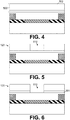
- a field-effect transistor (FET) structure (110) is first provided comprising a substrate (200) comprising a buried oxide layer (202;e.g. SiO 2 ) on a support layer (202), a channel region (330) on the buried oxide layer (202) in-between two source/drain regions (310,320), source/drain contacts (311,321) to the source/drain regions (310,320) and a dielectric layer (340) conformally covering the channel region (330), source/drain regions (310,320) and source/drain contacts (311,321).
- This FET structure (110) may be made based on methods which are well-known in the art.
- FIG. 2 A deep (e.g. around 50 to 100 ⁇ m deep) dry or wet etching is performed to open the bottom of the buried oxide layer (202), through the support layer (202). A freestanding FET structure is thereby obtained.
- a deep (e.g. around 50 to 100 ⁇ m deep) dry or wet etching is performed to open the bottom of the buried oxide layer (202), through the support layer (202).
- a freestanding FET structure is thereby obtained.
- a hardmask layer (501) (e.g. Al 2 O 3 ) is deposited over the dielectric layer (340), as part of a mask layer (500).
- a photoresist layer (502; e.g. poly(methyl methacrylate)), as part of the mask layer (500) is spin coated over the hardmask layer (501).
- the opening (510) is patterned down into the hardmask layer (501) using a dry or wet etching.
- the opening (510) is patterned down through the dielectric layer (340) and the channel region (330) using a dry or wet etching; forming a nanocavity (401) in the channel region (330).
- the etching is performed in such a way that the width of the nanocavity (401) tapers down towards the bottom of the nanocavity (401).
- a larger opening e.g. around 40 nm wide, may first be made, for example using deep ultraviolet lithography. This opening may then subsequently be shrunk (e.g. to around 20 to 24 nm) prior to transferring it into the channel region (not shown in the figures).
- Shrunk e.g. to around 20 to 24 nm
- Shrinking said opening may, for example, be achieved by conformally depositing a further mask lining into the opening, e.g. by atomic layer deposition (ALD), thereby reducing one or more lateral dimensions of the opening (not shown in these figures).
- the opening may for example first be transferred into the hardmask before shrinking it.
- shrinking said opening may, for example, also be achieved by forming the further mask lining using sequential infiltration synthesis (SIS).
- SIS sequential infiltration synthesis
- SIS can, for example, be performed on the photoresist itself, before transferring down the opening.
- At least the nanocavity (401) is conformally lined with a first gate dielectric (610; e.g. SiO 2 ), for example using ALD.
- a first gate dielectric 610; e.g. SiO 2
- the nanocavity (401) is filled with a protective material (402; e.g. a resist, a porous material or a solid-state material), in order to safeguard it during the subsequent process steps.
- a protective material e.g. a resist, a porous material or a solid-state material
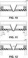
- Fig. 11 At least part of the buried oxide layer (202) is removed, thereby opening a bottom surface of the channel region (330) and, optionally, of the source/drain regions (310,320).
- Fig. 12 Using a dry or wet etching, the portion of the first gate dielectric (610) extending below the channel region (330) is removed.
- the protective material (402) is removed to open up the nanopore (400).
- a second gate dielectric (620; e.g. Al 2 O 3 ) is deposited on a bottom surface of the channel region (330) and, optionally, of the source/drain regions (310,320).
- a nanopore FET sensor (100) is thereby obtained, wherein the first orifice (410) of the nanopore (400) is delimited by the first gate dielectric (610) and the second orifice (420) is delimited by the second gate dielectric (620).
- SiO 2 may, for example, be selectively coated with a silane comprising -COOH groups, while Al 2 O 3 may be selectively coated with a phosphoric acid derivative comprising -NH 3 groups.
- first electrolyte solution to a first (e.g. 'cis') side of the nanopore FET sensor and contacting a second electrolyte solution to the second (e.g. 'trans') side of the nanopore FET sensor, wherein the first and second electrolyte solution differ in ionic strength.
- the difference in ionic strength can be achieved in several ways, e.g. by having a different concentration (e.g. 1 M vs. 1 mM), ionic charge (e.g. KCl vs. CaCl 2 vs. FeCl 3 ) and/or mobility (e.g. LiCl vs. KCl) of electrolytes on the first side with respect to the second side.
- Example 2 Various asymmetric nanopore architectures suitable for creating a non-linear potential profile
- the architecture of a nanopore can typically be decomposed into at least the vertical profile of the nanopore and the shape of its orifices.
- FIG. 15 showing vertical cross-sections of various exemplary asymmetric nanopore (400) profiles in accordance with embodiments of the present invention.
- a nanopore (400) having a width which tapers uniformly from the first orifice (410) to the second orifice (420) is shown.
- a nanopore (400) with a step-profile is shown; e.g. the width (w) of the nanopore (400) may have one or more discrete locations at which the nanopore width changes, but said width may otherwise be relatively constant.
- Fig. 15 showing vertical cross-sections of various exemplary asymmetric nanopore (400) profiles in accordance with embodiments of the present invention.
- a nanopore (400) with a step-profile is shown; e.g. the width (w) of the nanopore (400) may have one or more discrete locations at which the nanopore width changes
- a nanopore (400) having a constant width, but comprising subcomponents (431,432) of differing composition; the subcomponents (431,432) may, for example, have a difference in permittivity. While the subcomponents (431,432) shown here both extend substantially beyond the nanopore surface, the different composition may in embodiments also be limited to a difference at the nanopore surface.
- one material may define the nanopore (400), but it may comprise a first region defining a first portion of the nanopore (400) and having one surface chemical functionalization (e.g. its native surface functionalization), and a second region defining another portion of the nanopore (400) and having a differing surface chemical functionalization (e.g.
- FIG. 15d a nanopore (400) with a step-profile similar to Fig. 15b is shown, but wherein said step-profile is due to the presence of different subcomponents (431,432) akin to Fig. 15c .
- a nanopore (400) in accordance with Fig. 15d may, for example, be obtained by performing a selective epitaxial growth (e.g. selective epitaxial growth of Si) on a subcomponent of one composition (432), selectively with respect to a subcomponents of a different composition (431); thereby obtaining a change in width along the nanopore (400).
- a selective epitaxial growth e.g. selective epitaxial growth of Si
- FIG. 16 showing top views of exemplary nanopore (400) architectures with different orifice shapes.
- a nanopore (400) having a first (410) and second (420) orifice both having a circular shape is shown.
- a nanopore (400) with a first (410) and second (420) orifice both having a square shape is shown.
- the orifices may have other shapes (e.g. oval, rectangular, polygonal, etc.) and the shape of the first orifice need not be the same as that of the second orifice.
- the potential profile of a symmetric nanopore having a uniform width and nature across the entire depth, a step-profile asymmetric nanopore and a uniformly tapering asymmetric nanopore are shown, both in an empty (i.e. containing a fluid, but no analyte; full line) and filled (i.e. containing an analyte; dashed line) state.
- the potential profile of the symmetric nanopore barely differs between the filled state and the empty state (very small ⁇ V 1 ), complicating the detection of the presence of the analyte.
- the potential profile in the filled state is considerably different from that in the empty state (large ⁇ V 2 and ⁇ V 3 ); e.g. a difference of 10% or more, or even 30% or more can be observed.
- This potential difference is furthermore typically amplified in the FET, thereby yielding a relatively huge change in the channel current between the empty and filled state and greatly facilitating detection of the analyte.
- a nanopore FET (100) comprising a channel region (330) with a nanopore (400) therein, in-between two source/drain regions (310,320).
- the channel region (330) comprises a first portion (331) containing the nanopore (400) and two second portions (332), each defined in-between said nanopore-containing portion (331) and a source/drain region (310 or 320).
- the first portion (331) differs from the second portions (332) in that a doping concentration therein is lower than a doping concentration in the second portions (332).
- the first portion (331) may differ from the second portions (332) in that a bandgap therein is smaller than a bandgap in the second portions (332).
- the effect of the lower doping concentration and/or smaller bandgap is that the channel current through the channel region (330) predominantly depends on the first portion (331). Any change in this first portion (331), e.g. in the nanopore (400), will thus have an increased effect on the channel current. In turn, the sensitivity of the nanopore FET (100) for sensing an analyte in the nanopore (400) is thereby heightened.
- the nanopore When forming the nanopore in the channel region, the nanopore is preferably aligned such that the nanopore runs through the channel of the channel region and interact therewith. However, during manufacture, it may be difficult to ensure that each nanopore is well aligned and some misalignment may nevertheless occur in some devices.
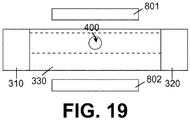
- a nanopore FET (100) comprising a channel region (330) with a nanopore (400) therein, in-between two source/drain regions (310,320); the nanopore (400) being slightly laterally misaligned with respect to the centre of the channel region (330).
- the nanopore FET (100) additionally comprises two side gates (801,802) laterally positioned with respect to the channel region (330), which can be used to align the channel inside the channel region (330) by applying a voltage across the side gates (801,802).
- the side gates (801,802) advantageously allow to correct for a degree of misalignment of the nanopore (400) and can thus increase the interaction between both.
- a smaller nanopore width a higher nanopore, an inclination angle between 5 and 80° (preferably between 30 and 45°, such as 37°), using different gate dielectric compositions (as is e.g. shown in example 1) and using a differently charged gate dielectric surface (wherein the first gate dielectric, on the cis side, is preferably more negatively charged than the second dielectric, on the trans side).
Landscapes
- Engineering & Computer Science (AREA)
- Health & Medical Sciences (AREA)
- Chemical & Material Sciences (AREA)
- Life Sciences & Earth Sciences (AREA)
- Physics & Mathematics (AREA)
- Biomedical Technology (AREA)
- Immunology (AREA)
- Pathology (AREA)
- Nanotechnology (AREA)
- General Physics & Mathematics (AREA)
- Molecular Biology (AREA)
- General Health & Medical Sciences (AREA)
- Biochemistry (AREA)
- Analytical Chemistry (AREA)
- Microelectronics & Electronic Packaging (AREA)
- Chemical Kinetics & Catalysis (AREA)
- Electrochemistry (AREA)
- Medicinal Chemistry (AREA)
- Food Science & Technology (AREA)
- Urology & Nephrology (AREA)
- Hematology (AREA)
- Biophysics (AREA)
- Spectroscopy & Molecular Physics (AREA)
- Investigating Or Analyzing Materials By The Use Of Electric Means (AREA)
- Thin Film Transistor (AREA)
Abstract
i. a source region (310) and a drain region (320), defining a source-drain axis;
ii. a channel region (330) between the source region (310) and the drain region (320);
iii. a nanopore (400) through the channel region (330), oriented at an angle to the source-drain axis, having a first orifice (410) and a second orifice (420), and being adapted for creating a non-linear potential profile between the first (410) and second (420) orifice.
Description
- The present invention relates to the field of field-effect transistor sensors; more particularly to nanopore field-effect transistor sensors.
- Biosensors have been developed intensively during the last decades and have enabled a wide set of applications in life sciences. As a very special biosensors, nanopore sensors provide the unique advantage of single molecule sensitivity; thereby having a great potential for single molecule studies and DNA sequencing. A first sequencing strategy by means of a nanopore is based on electrophoresis driven DNA translocation through the nanopore and subsequently monitoring the blockade effect of DNA on the ionic current flow through this nanopore. The underlying nucleotide sequence information may then be derivable from the fluctuations of the resulting signals.
- Revealing this sequence, however, requires the solving of several fundamental problems. Major challenges include: (1) to extract the correct sequence information, for which sensitivity and accuracy at the single nucleotide level are required; (2) to effectively control the molecular motions; (3) to obtain a high throughput readout, and (4) to fabricate reliable devices. In the past decades, many different paths have been tried and developed to overcome these problems.
- A first approach is based on the use of transmembrane protein channels as bio-nanopores. Bio-nanopores offer the specific advantage of an extremely well-defined shape, size and local charge distribution and the possibility to engineer these parameters using established molecular engineering technologies. In addition, bio-nanopores can be combined relatively easily with other biochemical technologies to control DNA motion. As such, bio-nanopore sensing has achieved a noticeable success and is, up to now, the only commercialized nanopore approach for deciphering genomes and other biomedical applications. However, drawbacks of this technique are the susceptible lipid membrane and bio-nanopores and the weak current signals (-pA) preventing the move towards higher throughput and robustness.
- Therefore, considerable research was performed on alternative nanopores, especially solid-state nanopores. Different solid-state nanopore technologies have been developed and show feasibility on single-molecular sensing, but none can solve all challenges, especially the intrinsic conflicts between current intensity, spatial resolution, and sensitivity.
- Xie et al. (2012) have shown that a solid-state nanopore combined with a synthesized silicon nanowire field-effect transistor (FET) can detect single molecules based on the fluctuations of local liquid potential during DNA translocations (Xie, Ping, et al. "Local electrical potential detection of DNA by nanowire-nanopore sensors." Nature nanotechnology 7.2 (2012): 119-125). Rather than modulating the ionic current through the pore, the blockade effect caused by DNA translocations can thus directly change the distribution of the local fluidic potentials inside the pore and sequentially modulate and amplify the transistor current of a FET near the pore; comparable to gating in a traditional FET. Potential sensing through transistors is an active method and avoids the need for a highly sensitive and passive measurement of the corresponding ionic current. Xie et al. reported that the transistor current (∼60 nA) was considerably larger than its corresponded ionic current (∼4 nA) through the same pore. This offers significant advantages, especially with respect to the scalability of the measurement technique. Ionic measurements need stable electrodes (one pair per nanopore), strict galvanic separation between different channels and highly sensitive current amplifiers. In contrast thereto, modulating the signal in a transistor circuit with the nanopore potential has the ability to overcome some of these challenges.
- Other results on this type of nanopore read-out have been based on 2D materials, such as graphene and MoS2. Although these materials indeed have very interesting properties, they still lack the maturity of the silicon platform, making it difficult to achieve a parallelized read-out scheme with millions of nanopores per chip.
- There is thus still a need in the art for nanopore field-effect transistor sensors with a sufficient sensitivity and sufficient spatial resolution, which can be manufactured in such a way as to allow parallelization and fast sampling rates.
- It is an object of the present invention to provide a good nanopore field-effect transistor sensor. It is a further object of the present invention to provide good methods for making said nanopore field-effect transistor sensor. The above objective is accomplished by products, methods and uses according to the present invention.
- It is an advantage of embodiments of the present invention that a nanopore field-effect transistor sensor with a large sensitivity (e.g. sufficient to identify single molecules) can be obtained.
- It is an advantage of embodiments of the present invention that a nanopore field-effect transistor sensor with a high spatial resolution (e.g. sufficient to identify single nucleotides in a DNA strand) can be obtained.
- It is an advantage of embodiments of the present invention that a relatively large number (e.g. an array) of nanopore field-effect transistor sensors can be formed on a single substrate. It is yet a further advantage of embodiments of the present invention that a relatively large number of sensing actions, of the same or of different analyte solutions, can be performed simultaneously; thereby speeding up the overall measurement to increase the throughput or achieving a higher accuracy in the same time span. It is a further advantage of embodiments of the present invention that the malfunction of a nanopore field-effect transistor in the plurality of nanopore field-effect transistor working in parallel can have a low effect on the overall performance of the device.
- It is an advantage of embodiments of the present invention that the nanopore field-effect transistor sensor may be relatively inexpensive to manufacture, even in large numbers.
- It is an advantage of embodiments of the present invention that the nanopore field-effect transistor sensor can be made using well-known techniques from semiconductor technology (e.g. CMOS technology). It is a further advantage of embodiments of the present invention that the nanopore field-effect transistor sensor can be made in a way that is compatible with other semiconductor devices and that they can be integrated therewith on a single substrate.
- In a first aspect, the present invention relates to a nanopore field-effect transistor sensor, comprising
- i. a source region and a drain region, defining a source-drain axis;
- ii. a channel region between the source region and the drain region;
- iii. a nanopore through the channel region, oriented at an angle to the source-drain axis, having a first and a second orifice, and being adapted for creating a non-linear potential profile between the first and second orifice.
- In a second aspect, the present invention relates to a nanopore field-effect transistor sensor array, comprising at least 50 nanopore field-effect transistor sensors according to any embodiment of the first aspect, preferably at least 100, yet more preferably at least 1000.
- In a third aspect, the present invention relates to a system comprising:
- i. the nanopore field-effect transistor sensor according to any embodiment of the first aspect,
- ii. a first electrolyte solution contacting the first orifice of the nanopore , and
- iii. a second electrolyte solution contacting the second orifice of the nanopore .
- In a fourth aspect, the present invention relates to a method for forming a nanopore field-effect transistor sensor, comprising:
- a. providing a structure comprising:
- i. a substrate,
- ii. a source region and a drain region in the substrate, defining a source-drain axis;
- iii. a channel region between the source region and the drain region,
- iv. optionally a layer on the channel region, and
- v. a mask layer over the channel region and the optional layer, the mask layer comprising an opening therethrough overlaying the channel region, the opening having a first width and being oriented at an angle to the source-drain axis;
- b. optionally, shrinking the opening such that the first width is reduced to a second width;
- c. etching the optional layer if present and the channel region through the opening, thereby forming a nanocavity;
- d. optionally, shrinking a width of the nanocavity.
- e. optionally, removing the mask layer;
- f. forming the nanopore from the nanocavity by opening the substrate underneath the nanocavity; the nanopore having a first orifice delimited by a first edge and a second orifice delimited by a second edge;
- performing step c of etching the channel region through the opening by anisotropically etching the channel region, and the optional layer if present, in such a way that the first orifice and the second orifice differ in area, and/or by
- modifying the first edge and/or the second edge so that they differ in chemical nature and/or so that they are made of dielectric material differing in thickness.
- In a fifth aspect, the present invention relates to a use of a non-linear potential profile for increasing a sensitivity and/or a spatial resolution of a nanopore field-effect transistor sensor.
- Particular and preferred aspects of the invention are set out in the accompanying independent and dependent claims. Features from the dependent claims may be combined with features of the independent claims and with features of other dependent claims as appropriate and not merely as explicitly set out in the claims.
- Although there has been constant improvement, change and evolution of devices in this field, the present concepts are believed to represent substantial new and novel improvements, including departures from prior practices, resulting in the provision of more efficient, stable and reliable devices of this nature.
- The above and other characteristics, features and advantages of the present invention will become apparent from the following detailed description, taken in conjunction with the accompanying drawings, which illustrate, by way of example, the principles of the invention. This description is given for the sake of example only, without limiting the scope of the invention. The reference figures quoted below refer to the attached drawings.
-
-
Figs. 1 to 14 are schematic representations of vertical cross-sections through intermediate structures along the fabrication of a FET sensor, in accordance with an exemplary embodiment of the present invention. -
Fig. 15 shows vertical cross-sections through channels in accordance with exemplary embodiments of the present invention. -
Fig. 16 shows top views of nanopore architectures with different orifice shapes, in accordance with exemplary embodiments of the present invention. -
Fig. 17 shows characteristic potential profile curves for three different nanopores, two of which are asymmetric nanopores in accordance with exemplary embodiments of the present invention. -
Fig. 18 is a schematically representation of a nanopore FET comprising differing channel region portions, in accordance with exemplary embodiments of the present invention. -
Fig. 19 is a schematically representation of a nanopore FET comprising side gates, in accordance with exemplary embodiments of the present invention. - In the different figures, the same reference signs refer to the same or analogous elements.
- The present invention will be described with respect to particular embodiments and with reference to certain drawings but the invention is not limited thereto but only by the claims. The drawings described are only schematic and are non-limiting. In the drawings, the size of some of the elements may be exaggerated and not drawn on scale for illustrative purposes. The dimensions and the relative dimensions do not correspond to actual reductions to practice of the invention.
- Furthermore, the terms first, second, third and the like in the description and in the claims, are used for distinguishing between similar elements and not necessarily for describing a sequence, either temporally, spatially, in ranking or in any other manner. It is to be understood that the terms so used are interchangeable under appropriate circumstances and that the embodiments of the invention described herein are capable of operation in other sequences than described or illustrated herein.
- Moreover, the terms top, bottom, over, under and the like in the description and the claims are used for descriptive purposes and not necessarily for describing relative positions. It is to be understood that the terms so used are interchangeable with their antonyms under appropriate circumstances and that the embodiments of the invention described herein are capable of operation in other orientations than described or illustrated herein.
- It is to be noticed that the term "comprising", used in the claims, should not be interpreted as being restricted to the means listed thereafter; it does not exclude other elements or steps. It is thus to be interpreted as specifying the presence of the stated features, integers, steps or components as referred to, but does not preclude the presence or addition of one or more other features, integers, steps or components, or groups thereof. Thus, the scope of the expression "a device comprising means A and B" should not be limited to devices consisting only of components A and B. It means that with respect to the present invention, the only relevant components of the device are A and B.
- Reference throughout this specification to "one embodiment" or "an embodiment" means that a particular feature, structure or characteristic described in connection with the embodiment is included in at least one embodiment of the present invention. Thus, appearances of the phrases "in one embodiment" or "in an embodiment" in various places throughout this specification are not necessarily all referring to the same embodiment, but may. Furthermore, the particular features, structures or characteristics may be combined in any suitable manner, as would be apparent to one of ordinary skill in the art from this disclosure, in one or more embodiments.
- Similarly, it should be appreciated that in the description of exemplary embodiments of the invention, various features of the invention are sometimes grouped together in a single embodiment, figure, or description thereof for the purpose of streamlining the disclosure and aiding in the understanding of one or more of the various inventive aspects. This method of disclosure, however, is not to be interpreted as reflecting an intention that the claimed invention requires more features than are expressly recited in each claim. Rather, as the following claims reflect, inventive aspects lie in less than all features of a single foregoing disclosed embodiment. Thus, the claims following the detailed description are hereby expressly incorporated into this detailed description, with each claim standing on its own as a separate embodiment of this invention.
- Furthermore, while some embodiments described herein include some but not other features included in other embodiments, combinations of features of different embodiments are meant to be within the scope of the invention, and form different embodiments, as would be understood by those in the art. For example, in the following claims, any of the claimed embodiments can be used in any combination.
- Furthermore, some of the embodiments are described herein as a method or combination of elements of a method that can be implemented by means of carrying out the function. Thus, an element described herein of an apparatus embodiment is an example of a means for carrying out the function performed by the element for the purpose of carrying out the invention.
- In the description provided herein, numerous specific details are set forth. However, it is understood that embodiments of the invention may be practised without these specific details. In other instances, well-known methods, structures and techniques have not been shown in detail in order not to obscure an understanding of this description.
- Reference will be made to transistors. These are devices having a first main electrode such as a drain, a second main electrode such as a source and a control electrode such as a gate for controlling the flow of electrical charges between the first and second main electrodes.
- The following terms are provided solely to aid in the understanding of the invention.
- As used herein, and unless otherwise specified, a nanocavity is an opening in a layer (e.g. in an FET channel or in an FET channel and in one or more overlaying layers such as overlaying dielectric layers) having at least one lateral dimension (width and/or length) ranging from 1 nm to 500 nm, preferably from 1 nm to 100 nm; preferably all dimensions of the nanocavity may range from 1 nm to 500 nm. The nanocavity may, for example, be defined by a width, a length, and a depth (or height), wherein the depth is typically a dimension perpendicular to a surface of the nanocavity-comprising layer. Preferably both width and length may range from 1 nm to 500 nm, preferably from 1 nm to 100 nm. Preferably all of the width, length and depth may range from 1 nm to 500 nm, preferably from 1 nm to 100 nm. The nanocavity is not typically limited by its shape and any cross-section therethrough may typically have any shape (e.g. triangular, rectangular, square, oval, circular, irregular, etc.); for example: an orifice of the nanocavity, co-planar with a surface of the nanocavity-comprising layer, may have any of the aforementioned shapes. In some embodiments, the nanocavity may have a depth smaller than a thickness of the nanocavity-comprising layer, such that a bottom of the nanocavity is defined within said layer. In other embodiments, the nanocavity may have a depth within 5% of the thickness of the nanocavity-comprising layer, while nevertheless having a closed bottom. In yet other embodiments, the nanocavity may completely cross through the nanocavity-comprising layer, thereby having both a top and a bottom of the nanocavity opening up to the surroundings; such a nanocavity is herein referred to as a nanopore. Such a nanopore may, for example, open up to a sensor cavity on one side and open up to another fluidic cavity on the opposite side.
- When a layer has an opening therein, said opening varying in section along its depth, said opening having a narrower portion having a section having at least one lateral dimension ranging from 1 nm to 500 nm and a broader portion having a section having both lateral dimensions above 500 nm, only the narrower portion of the opening is considered to be a nanocavity.
- As used herein and unless specified otherwise, a layer can be a single layer or can be formed of a plurality of sub-layers.
- As used herein, and unless otherwise specified, an asymmetric nanopore is a nanopore having an architecture such that there is no mirror plane between the first and second orifice, oriented perpendicular to an axis therebetween, which would allow the nanopore to be reflected onto itself. An asymmetric nanopore may be preferred in a nanopore field-effect transistor sensor according to the present invention, as it typically allows a potential profile, which is created between a first and a second orifice of the nanopore during operation of the sensor, to be non-linear.
- As used herein, and unless otherwise specified, under 'source/drain' is understood a 'source and/or drain'. Likewise under 'source/drain entity', e.g. source/drain region, is understood a 'source entity and/or drain entity', e.g. a source region and/or drain region. In embodiments, a source and a drain may be comparable (e.g. indistinguishable) and their designation may depend on a relative voltage difference that is put across them in the final device.
- In a first aspect, the present invention relates to a nanopore field-effect transistor sensor, comprising
- i. a source region and a drain region, defining a source-drain axis;
- ii. a channel region between the source region and the drain region;
- iii. a nanopore through the channel region, oriented at an angle to the source-drain axis, having a first and a second orifice, and being adapted for creating a non-linear potential profile between the first and second orifice.
- The field-effect transistor (FET) sensor may further comprise conventional elements as are well known to the skilled person. In embodiments, the FET sensor may be formed on a semiconductor substrate (e.g. a Si wafer, a silicon-on-insulator substrate or an epitaxial stack). In embodiments, the FET sensor may be formed on a group IV (e.g. Si) or group III-V (e.g. GaN) layer on a semiconductor substrate. Likewise, the source/drain regions may typically be of conventional design. Source and drain contacts may connect to the source/drain regions. During operation, an analyte solution may be present in the nanopore and sensing by the FET sensor may be based on gating of the channel current by the analyte. In preferred embodiments, the analyte may be charged. In embodiments, the field-effect transistor sensor may be a chemical sensor, such as a sensor for sensing a chemical (e.g. an ionic species) or a pH, and/or it may be a biological sensor, such as a sensor for sensing a biomolecule (e.g. a nucleotide in a nucleic acid, such as DNA or RNA). A biological sensor may typically be thought of as a specific case of a chemical sensor. In embodiments, the field-effect transistor sensor may be considered to be an ion-sensitive field-effect transistor (ISFET) or a field-effect transistor-based biosensor (BioFET).
- In embodiments, the channel region may have a width of from 2 nm to 250 nm, and/or a length of from 2 to 1000 nm, and/or a height of from 0.1 to 50 nm. In embodiments, the channel region may have one or more layers thereon. Preferably, the channel region may have a dielectric layer thereon.
- In embodiments, the nanopore field-effect transistor sensor may further comprise a layer, preferably a dielectric layer, on the channel region.
- In embodiments, the nanopore may be present at least partly through that layer.
- In embodiments, the dielectric layer may have a thickness over the channel region of from 1 to 100 nm. In embodiments, at least a portion of the dielectric layer thickness may be a membrane for protecting the channel region from damage or contamination. In embodiments, the nanopore may be lined by a gate dielectric layer. In embodiments, different portions of the nanopore may be lined by different gate dielectric layers. In embodiments, the gate dielectric layer may be selected from SiO2, Si3N4, Al2O3, HfO2, TiO2 and Ta2O5. In embodiments, the gate dielectric layer lining the nanopore may have a thickness inside the nanopore of from 1 to 10 nm. In embodiments, the first orifice may open on a first sensor cavity and/or the second orifice may open on a second sensor cavity. The sensor cavity typically has both lateral dimensions larger than 500 nm. In embodiments, the first sensor cavity may comprise a first electrolyte solution and/or the second sensor cavity may comprise a second electrolyte solution. In embodiments, sensing an analyte using the field-effect transistor sensor may comprise moving the analyte from the first sensor cavity (i.e. from the 'cis' side of the FET sensor), through the nanopore, towards the second sensor cavity (i.e. towards the 'trans' side of the FET sensor). In embodiments, the channel region may be closer to the second orifice than to the first orifice. In embodiments, the channel region (e.g. particularly the channel therein) may be at a distance of from 0 to 5 nm of the second orifice.
- In embodiments, the channel region may comprise:
- ia. a first channel region portion comprising the nanopore, and
- ib. a second channel region portion not comprising the nanopore; and
- the first channel region portion has a doping concentration which is at least 2 times lower (e.g. up to 100 times lower) than a doping concentration of the second channel region portion, and/or
- the first channel region portion has a bandgap which is at least 5% smaller (e.g. up to 90% smaller) than a bandgap of the second channel region portion.
- In embodiments, the length of the first channel region portion may be from 1% to 50% of the channel region length. In embodiments, the length of the first channel region portion may be from 10 nm to 500 nm. In embodiments, a minimum distance between an edge of the first channel region portion and the nanopore comprised in said portion may be at least from 1 to 100 nm. By having the lower doping concentration and/or smaller bandgap in the first channel region portion, a channel current through the channel region may be dominated by the characteristics of the said first portion. A change in this first portion, e.g. in the nanopore, will then result in a larger change of the channel current. In turn, the sensitivity of the nanopore FET for sensing an analyte in the nanopore is thus advantageously increased.
- It was surprisingly found within the present invention that the change (ΔV) of a non-linear potential profile in a FET sensor between a filled state of the nanopore (i.e. containing an analyte) and an empty state of the nanopore (i.e. containing a fluid, but no analyte) is relatively large (cf. example 3). Conversely, such a change is comparatively absent for a linear potential profile. It was therefore found particularly advantageous to make a nanopore FET sensor based on a nanopore which is inherently adapted for creating a non-linear potential profile between the first and second orifice (i.e. along an axis between the first and second orifice). Various possibilities exist for designing such a nanopore. In preferred embodiments, the nanopore may be an asymmetric nanopore. Asymmetric nanopores, whether they be asymmetric due to their general shape, due to the composition of the materials delimiting them or a combination thereof (cf. infra), typically advantageously yield nanopore FET sensors with a non-linear potential profile between the first and second orifice. In embodiments, the nanopore may be a symmetric nanopore. The above notwithstanding, some symmetric nanopores may also yield nanopore FET sensors with an asymmetric potential profile between the first and second orifice; for example, an hourglass-shaped nanopore. These nanopores may, however, be less preferred, as the change (ΔV) between the filled and empty state may typically be smaller for these symmetric nanopores. Furthermore, non-linear potential profiles created by symmetric nanopores often comprise an inflexion point at which there is no change between the empty and the filled state. In that case, it typically becomes particularly advantageous to control at which point along the nanopore the sensing is performed, in order to avoid said inflexion point.
- In embodiments, the first orifice may differ from the second orifice thereby creating the non-linear potential profile between the first and second orifice. When the first orifice differs from the second orifice, an asymmetric nanopore is advantageously straightforwardly obtained.
- In embodiments, the cross-section of the nanopore may vary along the axis going from the first to the second orifice. This variation may be continuous or step-wise. In embodiments, the first orifice and the second orifice may differ in area and/or may be delimited by edges differing in chemical nature. In embodiments, the area of the first orifice may be larger than the area of the second orifice. In preferred embodiments, a larger degree of asymmetry may be created by combining e.g. an asymmetric shape of the nanopore with an asymmetric composition of the materials delimiting the nanopore. In such a case, the obtainable change (ΔV) between the filled and empty state may typically be increased.
- The nanopore is typically oriented at an angle (β) to the source-drain axis. The angle may for example be from 30 to 150°, preferably from 60 to 120°, more preferably from 85 to 95°, most preferably 90°. In embodiments, the nanopore may have a width (w) of from 1 to 150 nm. In embodiments, the nanopore may have a smallest width (e.g. at the second orifice) of from 1 to 20 nm, preferably from 2 to 10 nm, yet more preferably from 5 to 7 nm. Thinner nanopores (e.g. 10 nm or smaller) may advantageously yield a higher sensitivity. In embodiments, the nanopore may have a largest width (e.g. at the first orifice) of from 1 to 150 nm, preferably from 2 to 100 nm, yet more preferably from 5 to 40 nm. In embodiments, the nanopore may have a height (h) of from 1 to 150 nm, preferably from 5 to 100 nm, yet more preferably from 10 to 50 nm, such as 20 nm. Higher nanopores may advantageously yield a higher sensitivity. The nanopore typically comprises a first orifice corresponding to an opening on a first side towards a first sensor cavity (e.g. towards a first electrolyte solution) and a second orifice corresponding to an opening towards a second sensor cavity (e.g. towards a second electrolyte solution). The first and the second orifice may typically have any shape, such as triangular, rectangular, square, oval, circular, irregular, etc.
- In embodiments, the nanopore may taper from the first orifice towards the second orifice. In embodiments, an average inclination (α) of a tapered sidewall of the nanopore may be from 1 to 100°, preferably from 5 to 80°, such as 70°. In embodiments, the nanopore may taper smoothly (e.g. continuously) from the first orifice towards the second orifice (e.g. having the shape of a truncated cone, truncated pyramid or truncated hemisphere), or the nanopore may comprise a step-profile (e.g. a profile comprising one or more step-like discontinuities).
- In embodiments, the first orifice and the second orifice may be delimited by edges of different permittivity and/or different surface charge.
- In embodiments, the permittivity and/or the surface charge may vary along the axis going from the first orifice to the second orifice. This variation may be continuous or step-wise. Preferably, the charge becomes more positive or less negative from the first orifice to the second orifice. In embodiments, the first orifice may be delimited by an edge formed of a first gate dielectric layer and the second orifice may be delimited by an edge formed of a second gate dielectric layer, the first gate dielectric layer having a chemical composition (e.g. translating in a different permittivity) differing from a chemical composition of the second gate dielectric layer and/or the first gate dielectric layer having a thickness differing from a thickness of the second gate dielectric layer.
- In embodiments, the permittivity and/or the thickness of the dielectric layer may vary along the axis going from the first orifice to the second orifice. This variation may be continuous or step-wise. In embodiments, the first dielectric layer having the thickness differing from the thickness of the second dielectric layer may have a chemical composition in common with the second dielectric layer or may have a composition differing therefrom. In embodiments, the first and/or second dielectric layer may be made of a material selected from SiO2, Si3N4, Al2O3, HfO2, TiO2 and Ta2O5. In embodiments, the first dielectric layer may consist of SiO2 and the second dielectric layer may consist of Al2O3.
- A practical way to have the edges of the first and second orifices differing in their chemical nature is by lining the nanopore with a first gate dielectric layer, thereby forming the edge of the first (or second) orifice and coating the surface comprising the second (or first) orifice with a second gate dielectric layer, thereby forming the edge of the second (or first) orifice. This way, the thickness of the first gate dielectric layer (measured parallelly to the substrate surface, and typically perpendicularly to the axis going from the first orifice to the second orifice if this axis is at a 90° angle with the substrate surface) is also much smaller than the thickness of the second gate dielectric layer, which is advantageous.
- In embodiments, the first orifice and the second orifice may be delimited by edges differing in their surface chemical functionalization. In embodiments, the surface functionalization may vary along the axis going from the first orifice to the second orifice. This variation may be continuous or step-wise. In embodiments, the first orifice and/or the second orifice may be functionalized with a self-assembling monolayer (SAM). In embodiments, the self-assembling monolayer may be bonded to the dielectric layer (e.g. first or second dielectric layer). In embodiments, the first orifice may have the surface chemical functionalization which is more positively or more negatively charged than the surface chemical functionalization of the second orifice, preferably more negatively. While any difference between the surface charging of the orifices is typically advantageous, a larger improvement in sensitivity may be observed when the first orifice is negatively charged. The surface chemical functionalization of the first orifice may, for example, be acidic (e.g. comprising -COOH groups), while the surface chemical functionalization of the second orifice may be neutral. Alternatively, the surface chemical functionalization of the first orifice may be neutral, while the surface chemical functionalization of the second orifice may be basic (e.g. comprising -NH3 groups). In preferred embodiments, the surface chemical functionalization of the first orifice may be acidic (e.g. comprising -COOH groups), while the surface chemical functionalization of the second orifice may be basic (e.g. comprising -NH3 groups). In embodiments, the first dielectric may consist of SiO2 selectively coated with a silane (e.g. comprising -COOH groups) and the second dielectric may consist of Al2O3 selectively coated with a phosphoric acid derivative (e.g. comprising -NH3 groups). In embodiments, these chemical functionalization differences expressed for the first and second orifice may be expressed as differences along the axis going from the first orifice to the second orifice. These variations may be continuous or step-wise.
- In embodiments, the nanopore field-effect transistor sensor may further comprise one or more side gates, the side gates laterally positioned with respect to the channel region. The one or more side gates can advantageously be used to align the channel inside the channel region, by applying a voltage across the one or more side gates. Some degree of misalignment of the channel with respect to the nanopore can thereby be rectified, advantageously increasing the interaction between both.
- In embodiments, any feature of any embodiment of the first aspect may independently be as correspondingly described for any embodiment of any of the other aspects.
- In a second aspect, the present invention relates to a nanopore field-effect transistor sensor array, comprising at least 50 nanopore field-effect transistor sensors according to any embodiment of the first aspect, preferably at least 100, yet more preferably at least 1000.
- Nanopore field-effect transistors in accordance with the present invention can advantageously be made in relatively large numbers on a same substrate, which can allow a high degree of parallelization and/or a high throughput. Furthermore, they can be made using techniques that are compatible with current CMOS technology and can be integrated therewith in the same device.
- In embodiments, any feature of any embodiment of the second aspect may independently be as correspondingly described for any embodiment of any of the other aspects.
- In a third aspect, the present invention relates to a system comprising:
- i. the nanopore field-effect transistor sensor according to any embodiment of the first aspect,
- ii. a first electrolyte solution contacting the first orifice of the nanopore (e.g. at a 'cis' side of the channel region), and
- iii. a second electrolyte solution contacting the second orifice of the nanopore (e.g. at a 'trans' side of the channel region).
- In embodiments, the first electrolyte solution may have an ionic strength differing from an ionic strength of the second electrolyte solution. In embodiments, the first and/or second electrolyte solution may be a solution of a water-soluble salt. In embodiments, the ionic strength difference may be due to a difference in electrolyte charge (e.g. KCI vs. CaCl2 vs. FeCl3), concentration (e.g. 1 M vs. 1 mM) and/or mobility (e.g. e.g. LiCI vs. KCI) in the first electrolyte solution compared to the second electrolyte solution. Two different electrolyte solutions advantageously add another level of asymmetry to the nanopore FET system, thereby increasing the observable change (ΔV) in the potential profiles. In embodiments, a concentration of the electrolyte in the first and/or second electrolyte solution may be from 1 µM to 10 M, preferably from 1 mM to 1 M.
- In embodiments, any feature of any embodiment of the third aspect may independently be as correspondingly described for any embodiment of any of the other aspects.
- In a fourth aspect, the present invention relates to a method for forming a nanopore field-effect transistor sensor, comprising:
- a. providing a structure comprising:
- i. a substrate,
- ii. a source region and a drain region in the substrate, defining a source-drain axis;
- iii. a channel region between the source region and the drain region,
- iv. optionally a layer on the channel region, and
- v. a mask layer over the channel region and the optional layer, the mask layer comprising an opening therein overlaying the channel region, the opening having a first width and being oriented at an angle to the source-drain axis;
- b. optionally, shrinking the opening such that the first width is reduced to a second width;
- c. etching the optional layer if present and the channel region through the opening, thereby forming a nanocavity;
- d. optionally, shrinking a width of the nanocavity.
- e. optionally, removing the mask layer;
- f. forming the nanopore from the nanocavity by opening the substrate underneath the nanocavity; the nanopore having a first orifice delimited by a first edge and a second orifice delimited by a second edge;
- performing step c of etching the channel region through the opening by anisotropically etching the channel region and the optional layer if present in such a way that the first orifice and the second orifice differ in area, and/or by
- modifying the first edge and/or the second edge so that they differ in chemical nature and/or so that they are made of dielectric material differing in thickness.
- While methods in accordance with the fourth aspect may be preferred, it will be clear that other methods can exist for fabricating embodiments of the first, second and/or third aspect.
- The optional layer is preferably a dielectric layer.
- In embodiments, the first and the second edges may differ in chemical nature by virtue of differing in surface chemical functionalization.
- In embodiments, the channel region may be made of silicon.
- In embodiments, step b may be performed using atomic layer deposition or sequential infiltration synthesis.
- In embodiments, step d may be performed using selective epitaxial growth.
- In embodiments, any feature of any embodiment of the fourth aspect may independently be as correspondingly described for any embodiment of any of the other aspects.
- In a fifth aspect, the present invention relates to a use of a non-linear potential profile for increasing a sensitivity and/or a spatial resolution of a nanopore field-effect transistor sensor.
- In embodiments, the sensitivity may relate to a change in potential difference (e.g. between a filled state and an empty state; ΔV). The change in potential difference may for example be measured through a change in the measured channel current. In embodiments, the potential difference may be normalized (e.g. by dividing the potential difference by the measured potential in the empty state).
- In embodiments, any feature of any embodiment of the fifth aspect may independently be as correspondingly described for any embodiment of any of the other aspects.
- The invention will now be described by a detailed description of several embodiments of the invention. It is clear that other embodiments of the invention can be configured according to the knowledge of the person skilled in the art without departing from the true technical teaching of the invention, the invention being limited only by the terms of the appended claims.
- We now refer to
Fig. 1 . A field-effect transistor (FET) structure (110) is first provided comprising a substrate (200) comprising a buried oxide layer (202;e.g. SiO2) on a support layer (202), a channel region (330) on the buried oxide layer (202) in-between two source/drain regions (310,320), source/drain contacts (311,321) to the source/drain regions (310,320) and a dielectric layer (340) conformally covering the channel region (330), source/drain regions (310,320) and source/drain contacts (311,321). This FET structure (110) may be made based on methods which are well-known in the art. - We now refer to
Fig. 2 . A deep (e.g. around 50 to 100 µm deep) dry or wet etching is performed to open the bottom of the buried oxide layer (202), through the support layer (202). A freestanding FET structure is thereby obtained. - We now refer to
Fig. 3 . A hardmask layer (501) (e.g. Al2O3) is deposited over the dielectric layer (340), as part of a mask layer (500). - We now refer to
Fig. 4 . A photoresist layer (502; e.g. poly(methyl methacrylate)), as part of the mask layer (500) is spin coated over the hardmask layer (501). - We now refer to
Fig. 5 . A small opening (510), e.g. around 20 nm wide, is patterned into the photoresist layer (502), for example using electron-beam lithography, to obtain an intermediate structure (120). - We now refer to
Fig. 6 . The opening (510) is patterned down into the hardmask layer (501) using a dry or wet etching. - We now refer to
Fig. 7 . The opening (510) is patterned down through the dielectric layer (340) and the channel region (330) using a dry or wet etching; forming a nanocavity (401) in the channel region (330). The etching is performed in such a way that the width of the nanocavity (401) tapers down towards the bottom of the nanocavity (401). - As an alternative to patterning the small opening directly (as shown in
Fig. 5 ) and transferring it down through the channel region (as shown inFigs. 6 and7 ), a larger opening, e.g. around 40 nm wide, may first be made, for example using deep ultraviolet lithography. This opening may then subsequently be shrunk (e.g. to around 20 to 24 nm) prior to transferring it into the channel region (not shown in the figures). Shrinking said opening may, for example, be achieved by conformally depositing a further mask lining into the opening, e.g. by atomic layer deposition (ALD), thereby reducing one or more lateral dimensions of the opening (not shown in these figures). To this end, the opening may for example first be transferred into the hardmask before shrinking it. Alternatively, shrinking said opening may, for example, also be achieved by forming the further mask lining using sequential infiltration synthesis (SIS). In that case, SIS can, for example, be performed on the photoresist itself, before transferring down the opening. - We now refer to
Fig. 8 . At least the nanocavity (401) is conformally lined with a first gate dielectric (610; e.g. SiO2), for example using ALD. - We now refer to
Fig. 9 . The photoresist layer (502) is removed. - We now refer to
Fig. 10 . The nanocavity (401) is filled with a protective material (402; e.g. a resist, a porous material or a solid-state material), in order to safeguard it during the subsequent process steps. - We now refer to
Fig. 11 . At least part of the buried oxide layer (202) is removed, thereby opening a bottom surface of the channel region (330) and, optionally, of the source/drain regions (310,320). - We now refer to
Fig. 12 . Using a dry or wet etching, the portion of the first gate dielectric (610) extending below the channel region (330) is removed. - We now refer to
Fig. 13 . The protective material (402) is removed to open up the nanopore (400). - We now refer to
Fig. 14 . Using ALD, evaporation or sputtering, a second gate dielectric (620; e.g. Al2O3) is deposited on a bottom surface of the channel region (330) and, optionally, of the source/drain regions (310,320). A nanopore FET sensor (100) is thereby obtained, wherein the first orifice (410) of the nanopore (400) is delimited by the first gate dielectric (610) and the second orifice (420) is delimited by the second gate dielectric (620). - Optionally, additional asymmetry may be created by selectively functionalizing one or both of the gate dielectrics. SiO2 may, for example, be selectively coated with a silane comprising -COOH groups, while Al2O3 may be selectively coated with a phosphoric acid derivative comprising -NH3 groups.
- Yet further asymmetry can optionally be introduced in the measuring system, by contacting a first electrolyte solution to a first (e.g. 'cis') side of the nanopore FET sensor and contacting a second electrolyte solution to the second (e.g. 'trans') side of the nanopore FET sensor, wherein the first and second electrolyte solution differ in ionic strength. The difference in ionic strength can be achieved in several ways, e.g. by having a different concentration (e.g. 1 M vs. 1 mM), ionic charge (e.g. KCl vs. CaCl2 vs. FeCl3) and/or mobility (e.g. LiCl vs. KCl) of electrolytes on the first side with respect to the second side.
- The architecture of a nanopore can typically be decomposed into at least the vertical profile of the nanopore and the shape of its orifices.
- We now refer to
Fig. 15 , showing vertical cross-sections of various exemplary asymmetric nanopore (400) profiles in accordance with embodiments of the present invention. InFig. 15a , a nanopore (400) having a width which tapers uniformly from the first orifice (410) to the second orifice (420) is shown. InFig. 15b , a nanopore (400) with a step-profile is shown; e.g. the width (w) of the nanopore (400) may have one or more discrete locations at which the nanopore width changes, but said width may otherwise be relatively constant. InFig. 15c , a nanopore (400) is shown having a constant width, but comprising subcomponents (431,432) of differing composition; the subcomponents (431,432) may, for example, have a difference in permittivity. While the subcomponents (431,432) shown here both extend substantially beyond the nanopore surface, the different composition may in embodiments also be limited to a difference at the nanopore surface. For example, one material may define the nanopore (400), but it may comprise a first region defining a first portion of the nanopore (400) and having one surface chemical functionalization (e.g. its native surface functionalization), and a second region defining another portion of the nanopore (400) and having a differing surface chemical functionalization (e.g. a non-native surface functionalization). InFig. 15d , a nanopore (400) with a step-profile similar toFig. 15b is shown, but wherein said step-profile is due to the presence of different subcomponents (431,432) akin toFig. 15c . A nanopore (400) in accordance withFig. 15d may, for example, be obtained by performing a selective epitaxial growth (e.g. selective epitaxial growth of Si) on a subcomponent of one composition (432), selectively with respect to a subcomponents of a different composition (431); thereby obtaining a change in width along the nanopore (400). - We now refer to
Fig. 16 , showing top views of exemplary nanopore (400) architectures with different orifice shapes. InFig. 16a , a nanopore (400) having a first (410) and second (420) orifice both having a circular shape is shown. InFig. 16b , a nanopore (400) with a first (410) and second (420) orifice both having a square shape is shown. In other embodiments, which are not depicted, the orifices may have other shapes (e.g. oval, rectangular, polygonal, etc.) and the shape of the first orifice need not be the same as that of the second orifice. - It will be clear that the orifice shapes and vertical profiles of the nanopore can be combined in a variety of ways to form different nanopore architectures; some examples include:
- a nanopore with a vertical profile as in
Fig. 15a and a top view as inFig. 16a , its general shape may thus correspond to that of a truncated cone; - a nanopore with a vertical profile as in
Fig. 15a and a top view as inFig. 16b , its general shape may thus correspond to that of a truncated pyramid; - a nanopore with a vertical profile as in
Fig. 15b and a top view as inFig. 16a or 16b ; - a nanopore with a vertical profile as in
Fig. 15c and its orifices may be circular or rectangular (corresponding top view not depicted), its general shape may thus correspond to that of a cylinder or cuboid comprising surfaces of different nature; - a nanopore with a vertical profile as in
Fig. 15d and its orifices may be circular or rectangular (corresponding top view not depicted); etc. - We now refer to
Fig. 17 , depicting characteristic potential profile curves for 20 nm long nanopores, going from their entrance (i.e. the cis orifice; Z = 0 nm) to their exit (i.e. the trans orifice; Z = 20 nm). The potential profile of a symmetric nanopore having a uniform width and nature across the entire depth, a step-profile asymmetric nanopore and a uniformly tapering asymmetric nanopore are shown, both in an empty (i.e. containing a fluid, but no analyte; full line) and filled (i.e. containing an analyte; dashed line) state. As shown inFig. 17 , the potential profile of the symmetric nanopore barely differs between the filled state and the empty state (very small ΔV1), complicating the detection of the presence of the analyte. Conversely, for both asymmetric nanopores, the potential profile in the filled state is considerably different from that in the empty state (large ΔV2 and ΔV3); e.g. a difference of 10% or more, or even 30% or more can be observed. This potential difference is furthermore typically amplified in the FET, thereby yielding a relatively huge change in the channel current between the empty and filled state and greatly facilitating detection of the analyte. - We now refer to
Fig. 18 , schematically depicting a nanopore FET (100) comprising a channel region (330) with a nanopore (400) therein, in-between two source/drain regions (310,320). The channel region (330) comprises a first portion (331) containing the nanopore (400) and two second portions (332), each defined in-between said nanopore-containing portion (331) and a source/drain region (310 or 320). The first portion (331) differs from the second portions (332) in that a doping concentration therein is lower than a doping concentration in the second portions (332). Alternatively, or additionally, the first portion (331) may differ from the second portions (332) in that a bandgap therein is smaller than a bandgap in the second portions (332). The effect of the lower doping concentration and/or smaller bandgap is that the channel current through the channel region (330) predominantly depends on the first portion (331). Any change in this first portion (331), e.g. in the nanopore (400), will thus have an increased effect on the channel current. In turn, the sensitivity of the nanopore FET (100) for sensing an analyte in the nanopore (400) is thereby heightened. - When forming the nanopore in the channel region, the nanopore is preferably aligned such that the nanopore runs through the channel of the channel region and interact therewith. However, during manufacture, it may be difficult to ensure that each nanopore is well aligned and some misalignment may nevertheless occur in some devices.
- We now refer to
Fig. 19 , schematically depicting a nanopore FET (100) comprising a channel region (330) with a nanopore (400) therein, in-between two source/drain regions (310,320); the nanopore (400) being slightly laterally misaligned with respect to the centre of the channel region (330). The nanopore FET (100) additionally comprises two side gates (801,802) laterally positioned with respect to the channel region (330), which can be used to align the channel inside the channel region (330) by applying a voltage across the side gates (801,802). In this way, the side gates (801,802) advantageously allow to correct for a degree of misalignment of the nanopore (400) and can thus increase the interaction between both. - Various simulations with nanopore field-effect transistor sensors having a non-linear potential profile were performed in order to validate their usefulness. It could be confirmed that a singly charged nanocube (1x1x1 nm) and a nanorod (1x1x15 nm) with 15 charges can both be successfully detected; e.g. as a change in the channel current of about 90 nA for the nanocube and about 900 nA for the nanorod, wherein the change is respectively with respect to an equivalent neutral nanocube (e.g. around 1.5 µA) and neutral nanorod (e.g. around 4 µA). Furthermore it was confirmed that the following factors can have a positive effect on the sensitivity: a smaller nanopore width, a higher nanopore, an inclination angle between 5 and 80° (preferably between 30 and 45°, such as 37°), using different gate dielectric compositions (as is e.g. shown in example 1) and using a differently charged gate dielectric surface (wherein the first gate dielectric, on the cis side, is preferably more negatively charged than the second dielectric, on the trans side).
- It is to be understood that although preferred embodiments, specific constructions and configurations, as well as materials, have been discussed herein for devices according to the present invention, various changes or modifications in form and detail may be made without departing from the scope and technical teachings of this invention. For example, any formulas given above are merely representative of procedures that may be used. Functionality may be added or deleted from the block diagrams and operations may be interchanged among functional blocks. Steps may be added or deleted to methods described within the scope of the present invention.
Claims (16)
- A nanopore field-effect transistor sensor (100), comprisingi. a source region (310) and a drain region (320), defining a source-drain axis;ii. a channel region (330) between the source region (310) and the drain region (320);iii. a nanopore (400) through the channel region (330), oriented at an angle to the source-drain axis, having a first orifice (410) and a second orifice (420), and being adapted for creating a non-linear potential profile between the first (410) and second (420) orifice.
- The nanopore field-effect transistor sensor (100) according to claim 1, wherein the first orifice (410) differs from the second orifice (420) thereby creating the non-linear potential profile between the first (410) and second (420) orifice.
- The nanopore field-effect transistor sensor (100) according to claim 2, wherein the first orifice (410) and the second orifice (420) differ in area and/or are delimited by edges differing in chemical nature.
- The nanopore field-effect transistor sensor (100) according to claim 3, wherein the nanopore (400) tapers from the first orifice (410) towards the second (420) orifice.
- The nanopore field-effect transistor sensor (100) according to claim 3 or 4, wherein the first orifice (410) and the second orifice (420) are delimited by edges of different permittivity and/or different surface charge.
- The nanopore field-effect transistor sensor (100) according to claim 5, wherein the first orifice (410) is delimited by an edge formed of a first gate dielectric layer (610) and the second orifice (420) is delimited by an edge formed of a second gate dielectric layer (620), the first gate dielectric layer (610) having a chemical composition differing from a chemical composition of the second gate dielectric layer (620) and/or the first gate dielectric layer (610) having a thickness differing from a thickness of the second gate dielectric layer (620).
- The nanopore field-effect transistor sensor (100) according to claim 5 or 6, wherein the first orifice (410) and the second orifice (420) are delimited by edges differing in their surface chemical functionalization.
- The nanopore field-effect transistor sensor (100) according to any of the previous claims, wherein the channel region (330) comprises:ia. a first channel region portion (331) comprising the nanopore (400), andib. a second channel region portion (332) not comprising the nanopore (400); andwherein- the first channel region portion (331) has a doping concentration which is at least 2 times lower than a doping concentration of the second channel region portion (332), and/or- the first channel region portion (331) has a bandgap which is at least 5% smaller than a bandgap of the second channel region portion (332).
- The nanopore field-effect transistor sensor (100) according to any of the previous claims, further comprising one or more side gates (801,802), the side gates (801,802) being laterally positioned with respect to the channel region (330).
- The nanopore field-effect transistor sensor (100) according to any of the previous claims, further comprising a layer (340) on the channel region (330).
- The nanopore field effect transistor sensor (100) according to claim 10, wherein the nanopore (400) is present at least partly through the layer (340).
- A nanopore field-effect transistor sensor (100) array, comprising at least 50 nanopore field-effect transistor sensors (100) according to any of claims 1 to 11, preferably at least 100, yet more preferably at least 1000.
- A system comprising:i. the nanopore field-effect transistor sensor (100) according to any of claims 1 to 11,ii. a first electrolyte solution contacting the first orifice (410) of the nanopore (400), andiii. a second electrolyte solution contacting the second orifice (420) of the nanopore (400).
- The system according to claim 13, wherein the first electrolyte solution has an ionic strength differing from an ionic strength of the second electrolyte solution.
- A method for forming a nanopore field-effect transistor sensor (100), comprising:a. providing a structure (120) comprising:i. a substrate (200),ii. a source region (310) and a drain region (320) on the substrate (200), defining a source-drain axis;iii. a channel region (330) between the source region (310) and the drain region (320), andiv. optionally a layer (340) on the channel region,v. a mask layer (500) over the channel region (330) and the optional layer (340) if present, the mask layer (500) comprising an opening (510) therethrough overlying the channel region (330), the opening (510) having a first width and being oriented at an angle to the source-drain axis;b. optionally, shrinking the opening (510) such that the first width is reduced to a second width;c. etching the optional layer (340) if present, and the channel region, (330) through the opening (510), thereby forming a nanocavity (401);d. optionally, shrinking a width of the nanocavity (401).e. optionally, removing the mask layer (500);f. forming the nanopore (400) from the nanocavity (401) by opening the substrate (200) underneath the nanocavity (401); the nanopore (400) having a first orifice (410) delimited by a first edge and a second orifice (420) delimited by a second edge;wherein the nanopore (400) is adapted for creating a non-linear potential profile between the first (410) and second (420) orifice by:- performing step c of etching the optional layer (340) if present and the channel region (300) through the opening (510) by anisotropically etching the channel region (300), and the optional layer if present, in such a way that the first orifice (410) and the second orifice (420) differ in area, and/or by- modifying the first edge and/or the second edge so that they differ in chemical nature and/or so that they are made of dielectric material differing in thickness.
- The method according to claim 15, wherein the first gate dielectric layer (610) and second gate dielectric layer (620) differ in chemical nature by virtue of differing in surface chemical functionalization.
Priority Applications (3)
| Application Number | Priority Date | Filing Date | Title |
|---|---|---|---|
| EP17210422.6A EP3502688B1 (en) | 2017-12-22 | 2017-12-22 | Nanopore fet sensor with non-linear potential profile |
| US16/761,712 US11367797B2 (en) | 2017-12-22 | 2018-07-24 | Nanopore FET sensor with non-linear potential profile |
| PCT/EP2018/070007 WO2019120642A1 (en) | 2017-12-22 | 2018-07-24 | Nanopore fet sensor with non-linear potential profile |
Applications Claiming Priority (1)
| Application Number | Priority Date | Filing Date | Title |
|---|---|---|---|
| EP17210422.6A EP3502688B1 (en) | 2017-12-22 | 2017-12-22 | Nanopore fet sensor with non-linear potential profile |
Publications (2)
| Publication Number | Publication Date |
|---|---|
| EP3502688A1 true EP3502688A1 (en) | 2019-06-26 |
| EP3502688B1 EP3502688B1 (en) | 2019-11-13 |
Family
ID=60811926
Family Applications (1)
| Application Number | Title | Priority Date | Filing Date |
|---|---|---|---|
| EP17210422.6A Active EP3502688B1 (en) | 2017-12-22 | 2017-12-22 | Nanopore fet sensor with non-linear potential profile |
Country Status (3)
| Country | Link |
|---|---|
| US (1) | US11367797B2 (en) |
| EP (1) | EP3502688B1 (en) |
| WO (1) | WO2019120642A1 (en) |
Cited By (1)
| Publication number | Priority date | Publication date | Assignee | Title |
|---|---|---|---|---|
| EP4075131A1 (en) * | 2021-04-16 | 2022-10-19 | Imec VZW | Nanopore transistor for biosensing |
Families Citing this family (3)
| Publication number | Priority date | Publication date | Assignee | Title |
|---|---|---|---|---|
| JP2024512838A (en) * | 2021-03-31 | 2024-03-21 | イルミナ インコーポレイテッド | Scalable circuit for molecular detection |
| EP4113112B1 (en) | 2021-06-30 | 2026-02-25 | Imec VZW | A method of operating a pore field-effect transistor sensor for detecting particles |
| US20240210343A1 (en) * | 2022-12-23 | 2024-06-27 | Imec Vzw | Nanopore sensing device with multiple sensing layers |
Citations (5)
| Publication number | Priority date | Publication date | Assignee | Title |
|---|---|---|---|---|
| US20100327847A1 (en) * | 2007-09-12 | 2010-12-30 | President And Fellows Of Harvard College | High-Resolution Molecular Sensor |
| JP2014190891A (en) * | 2013-03-28 | 2014-10-06 | Hitachi High-Technologies Corp | Voltage applying system of nanopore type analyzer |
| US20160033451A1 (en) * | 2014-10-07 | 2016-02-04 | National Institute Of Standards And Technology | Single molecule filter and single molecule electrograph, and process for making and using same |
| US20160187290A1 (en) * | 2013-04-18 | 2016-06-30 | The Board Of Trustees Of The University Of Illinois | Method and apparatus for analyzing a target material |
| US20160231307A1 (en) * | 2015-02-05 | 2016-08-11 | President And Fellows Of Harvard College | Nanopore Sensor Including Fluidic Passage |
Family Cites Families (1)
| Publication number | Priority date | Publication date | Assignee | Title |
|---|---|---|---|---|
| US9034637B2 (en) * | 2007-04-25 | 2015-05-19 | Nxp, B.V. | Apparatus and method for molecule detection using nanopores |
-
2017
- 2017-12-22 EP EP17210422.6A patent/EP3502688B1/en active Active
-
2018
- 2018-07-24 US US16/761,712 patent/US11367797B2/en active Active
- 2018-07-24 WO PCT/EP2018/070007 patent/WO2019120642A1/en not_active Ceased
Patent Citations (5)
| Publication number | Priority date | Publication date | Assignee | Title |
|---|---|---|---|---|
| US20100327847A1 (en) * | 2007-09-12 | 2010-12-30 | President And Fellows Of Harvard College | High-Resolution Molecular Sensor |
| JP2014190891A (en) * | 2013-03-28 | 2014-10-06 | Hitachi High-Technologies Corp | Voltage applying system of nanopore type analyzer |
| US20160187290A1 (en) * | 2013-04-18 | 2016-06-30 | The Board Of Trustees Of The University Of Illinois | Method and apparatus for analyzing a target material |
| US20160033451A1 (en) * | 2014-10-07 | 2016-02-04 | National Institute Of Standards And Technology | Single molecule filter and single molecule electrograph, and process for making and using same |
| US20160231307A1 (en) * | 2015-02-05 | 2016-08-11 | President And Fellows Of Harvard College | Nanopore Sensor Including Fluidic Passage |
Non-Patent Citations (1)
| Title |
|---|
| XIE, PING ET AL.: "Local electrical potential detection of DNA by nanowire-nanopore sensors", NATURE NANOTECHNOLOGY, vol. 7.2, 2012, pages 119 - 125 |
Cited By (2)
| Publication number | Priority date | Publication date | Assignee | Title |
|---|---|---|---|---|
| EP4075131A1 (en) * | 2021-04-16 | 2022-10-19 | Imec VZW | Nanopore transistor for biosensing |
| US12188895B2 (en) | 2021-04-16 | 2025-01-07 | Imec Vzw | Nanopore transistor for biosensing |
Also Published As
| Publication number | Publication date |
|---|---|
| US20210184053A1 (en) | 2021-06-17 |
| EP3502688B1 (en) | 2019-11-13 |
| US11367797B2 (en) | 2022-06-21 |
| WO2019120642A1 (en) | 2019-06-27 |
Similar Documents
| Publication | Publication Date | Title |
|---|---|---|
| US12411126B2 (en) | Nanopore sensor having a fluidic passage and transistor sensing of local electrical potential at the fluidic passage | |
| CN109313157B (en) | Nanopore sensor, structures and devices including the sensor, and methods of forming and using the same | |
| CN102242062B (en) | High-resolution biosensor | |
| US9989516B2 (en) | Electro-diffusion enhanced bio-molecule charge detection using electrostatic interaction | |
| US8518829B2 (en) | Self-sealed fluidic channels for nanopore array | |
| US11367797B2 (en) | Nanopore FET sensor with non-linear potential profile | |
| Yang et al. | Advances in nanopore sequencing technology | |
| US9658184B2 (en) | Increasing the capture zone by nanostructure patterns | |
| ITRM20110252A1 (en) | METHOD OF ANALYSIS OF SINGLE MOLECULA BY MEANS OF A COLLECTION OF A MOLECULE TARGET ON FUNCTIONALIZED NANOPORES. | |
| Fu et al. | Biomimetic stimuli‐responsive nanochannels and their applications | |
| Li et al. | Dynamics of DNA clogging in hafnium oxide nanopores | |
| CN107328838A (en) | A kind of electronic biosensor and preparation method based on bigrid single-electronic transistor | |
| Kim et al. | A dual-gate field-effect transistor for label-free electrical detection of avian influenza | |
| EP3620783B1 (en) | Field-effect transistor-based biosensor, method of fabrication thereof and method for detecting an analyte using said biosensor | |
| Taniguchi et al. | Nanopore device for single-molecule sensing method and its application | |
| CN114137377B (en) | Target molecule detection transistor sensor and preparation method thereof | |
| Reynaud | Aptamer-functionalized nanopore for the detection of closely-related proteins | |
| Vu | Silicon nanowire transistor arrays for biomolecular detection | |
| Liu et al. | Single-crystal silicon nanopore and arrays | |
| Chandra et al. | Fabrication process and Performance analysis of Ion Sensitive Field Effect transistor Sensor (ISFET) | |
| Khanna | ION-SENSITIVE FIELD-EFFECT TRANSISTORS WITH NANOSTRUCTURED CHANNELS AND NANOPARTICLE-MODIFIED GATE SURFACES |
Legal Events
| Date | Code | Title | Description |
|---|---|---|---|
| STAA | Information on the status of an ep patent application or granted ep patent |
Free format text: STATUS: EXAMINATION IS IN PROGRESS |
|
| PUAI | Public reference made under article 153(3) epc to a published international application that has entered the european phase |
Free format text: ORIGINAL CODE: 0009012 |
|
| 17P | Request for examination filed |
Effective date: 20180727 |
|
| AK | Designated contracting states |
Kind code of ref document: A1 Designated state(s): AL AT BE BG CH CY CZ DE DK EE ES FI FR GB GR HR HU IE IS IT LI LT LU LV MC MK MT NL NO PL PT RO RS SE SI SK SM TR |
|
| AX | Request for extension of the european patent |
Extension state: BA ME |
|
| GRAP | Despatch of communication of intention to grant a patent |
Free format text: ORIGINAL CODE: EPIDOSNIGR1 |
|
| STAA | Information on the status of an ep patent application or granted ep patent |
Free format text: STATUS: GRANT OF PATENT IS INTENDED |
|
| INTG | Intention to grant announced |
Effective date: 20190816 |
|
| GRAS | Grant fee paid |
Free format text: ORIGINAL CODE: EPIDOSNIGR3 |
|
| GRAA | (expected) grant |
Free format text: ORIGINAL CODE: 0009210 |
|
| STAA | Information on the status of an ep patent application or granted ep patent |
Free format text: STATUS: THE PATENT HAS BEEN GRANTED |
|
| AK | Designated contracting states |
Kind code of ref document: B1 Designated state(s): AL AT BE BG CH CY CZ DE DK EE ES FI FR GB GR HR HU IE IS IT LI LT LU LV MC MK MT NL NO PL PT RO RS SE SI SK SM TR |
|
| REG | Reference to a national code |
Ref country code: CH Ref legal event code: EP Ref country code: AT Ref legal event code: REF Ref document number: 1202213 Country of ref document: AT Kind code of ref document: T Effective date: 20191115 |
|
| REG | Reference to a national code |
Ref country code: DE Ref legal event code: R096 Ref document number: 602017008662 Country of ref document: DE |
|
| REG | Reference to a national code |
Ref country code: IE Ref legal event code: FG4D |
|
| REG | Reference to a national code |
Ref country code: NL Ref legal event code: MP Effective date: 20191113 |
|
| REG | Reference to a national code |
Ref country code: LT Ref legal event code: MG4D |
|
| PG25 | Lapsed in a contracting state [announced via postgrant information from national office to epo] |
Ref country code: BG Free format text: LAPSE BECAUSE OF FAILURE TO SUBMIT A TRANSLATION OF THE DESCRIPTION OR TO PAY THE FEE WITHIN THE PRESCRIBED TIME-LIMIT Effective date: 20200213 Ref country code: NO Free format text: LAPSE BECAUSE OF FAILURE TO SUBMIT A TRANSLATION OF THE DESCRIPTION OR TO PAY THE FEE WITHIN THE PRESCRIBED TIME-LIMIT Effective date: 20200213 Ref country code: GR Free format text: LAPSE BECAUSE OF FAILURE TO SUBMIT A TRANSLATION OF THE DESCRIPTION OR TO PAY THE FEE WITHIN THE PRESCRIBED TIME-LIMIT Effective date: 20200214 Ref country code: LT Free format text: LAPSE BECAUSE OF FAILURE TO SUBMIT A TRANSLATION OF THE DESCRIPTION OR TO PAY THE FEE WITHIN THE PRESCRIBED TIME-LIMIT Effective date: 20191113 Ref country code: FI Free format text: LAPSE BECAUSE OF FAILURE TO SUBMIT A TRANSLATION OF THE DESCRIPTION OR TO PAY THE FEE WITHIN THE PRESCRIBED TIME-LIMIT Effective date: 20191113 Ref country code: NL Free format text: LAPSE BECAUSE OF FAILURE TO SUBMIT A TRANSLATION OF THE DESCRIPTION OR TO PAY THE FEE WITHIN THE PRESCRIBED TIME-LIMIT Effective date: 20191113 Ref country code: PT Free format text: LAPSE BECAUSE OF FAILURE TO SUBMIT A TRANSLATION OF THE DESCRIPTION OR TO PAY THE FEE WITHIN THE PRESCRIBED TIME-LIMIT Effective date: 20200313 Ref country code: SE Free format text: LAPSE BECAUSE OF FAILURE TO SUBMIT A TRANSLATION OF THE DESCRIPTION OR TO PAY THE FEE WITHIN THE PRESCRIBED TIME-LIMIT Effective date: 20191113 Ref country code: PL Free format text: LAPSE BECAUSE OF FAILURE TO SUBMIT A TRANSLATION OF THE DESCRIPTION OR TO PAY THE FEE WITHIN THE PRESCRIBED TIME-LIMIT Effective date: 20191113 Ref country code: LV Free format text: LAPSE BECAUSE OF FAILURE TO SUBMIT A TRANSLATION OF THE DESCRIPTION OR TO PAY THE FEE WITHIN THE PRESCRIBED TIME-LIMIT Effective date: 20191113 |
|
| PG25 | Lapsed in a contracting state [announced via postgrant information from national office to epo] |
Ref country code: IS Free format text: LAPSE BECAUSE OF FAILURE TO SUBMIT A TRANSLATION OF THE DESCRIPTION OR TO PAY THE FEE WITHIN THE PRESCRIBED TIME-LIMIT Effective date: 20200313 Ref country code: RS Free format text: LAPSE BECAUSE OF FAILURE TO SUBMIT A TRANSLATION OF THE DESCRIPTION OR TO PAY THE FEE WITHIN THE PRESCRIBED TIME-LIMIT Effective date: 20191113 Ref country code: HR Free format text: LAPSE BECAUSE OF FAILURE TO SUBMIT A TRANSLATION OF THE DESCRIPTION OR TO PAY THE FEE WITHIN THE PRESCRIBED TIME-LIMIT Effective date: 20191113 |
|
| PG25 | Lapsed in a contracting state [announced via postgrant information from national office to epo] |
Ref country code: AL Free format text: LAPSE BECAUSE OF FAILURE TO SUBMIT A TRANSLATION OF THE DESCRIPTION OR TO PAY THE FEE WITHIN THE PRESCRIBED TIME-LIMIT Effective date: 20191113 |
|
| PG25 | Lapsed in a contracting state [announced via postgrant information from national office to epo] |
Ref country code: ES Free format text: LAPSE BECAUSE OF FAILURE TO SUBMIT A TRANSLATION OF THE DESCRIPTION OR TO PAY THE FEE WITHIN THE PRESCRIBED TIME-LIMIT Effective date: 20191113 Ref country code: RO Free format text: LAPSE BECAUSE OF FAILURE TO SUBMIT A TRANSLATION OF THE DESCRIPTION OR TO PAY THE FEE WITHIN THE PRESCRIBED TIME-LIMIT Effective date: 20191113 Ref country code: CZ Free format text: LAPSE BECAUSE OF FAILURE TO SUBMIT A TRANSLATION OF THE DESCRIPTION OR TO PAY THE FEE WITHIN THE PRESCRIBED TIME-LIMIT Effective date: 20191113 Ref country code: DK Free format text: LAPSE BECAUSE OF FAILURE TO SUBMIT A TRANSLATION OF THE DESCRIPTION OR TO PAY THE FEE WITHIN THE PRESCRIBED TIME-LIMIT Effective date: 20191113 Ref country code: EE Free format text: LAPSE BECAUSE OF FAILURE TO SUBMIT A TRANSLATION OF THE DESCRIPTION OR TO PAY THE FEE WITHIN THE PRESCRIBED TIME-LIMIT Effective date: 20191113 |
|
| REG | Reference to a national code |
Ref country code: DE Ref legal event code: R097 Ref document number: 602017008662 Country of ref document: DE |
|
| REG | Reference to a national code |
Ref country code: AT Ref legal event code: MK05 Ref document number: 1202213 Country of ref document: AT Kind code of ref document: T Effective date: 20191113 |
|
| REG | Reference to a national code |
Ref country code: BE Ref legal event code: MM Effective date: 20191231 |
|
| PG25 | Lapsed in a contracting state [announced via postgrant information from national office to epo] |
Ref country code: MC Free format text: LAPSE BECAUSE OF FAILURE TO SUBMIT A TRANSLATION OF THE DESCRIPTION OR TO PAY THE FEE WITHIN THE PRESCRIBED TIME-LIMIT Effective date: 20191113 Ref country code: SK Free format text: LAPSE BECAUSE OF FAILURE TO SUBMIT A TRANSLATION OF THE DESCRIPTION OR TO PAY THE FEE WITHIN THE PRESCRIBED TIME-LIMIT Effective date: 20191113 Ref country code: SM Free format text: LAPSE BECAUSE OF FAILURE TO SUBMIT A TRANSLATION OF THE DESCRIPTION OR TO PAY THE FEE WITHIN THE PRESCRIBED TIME-LIMIT Effective date: 20191113 |
|
| PLBE | No opposition filed within time limit |
Free format text: ORIGINAL CODE: 0009261 |
|
| STAA | Information on the status of an ep patent application or granted ep patent |
Free format text: STATUS: NO OPPOSITION FILED WITHIN TIME LIMIT |
|
| 26N | No opposition filed |
Effective date: 20200814 |
|
| PG25 | Lapsed in a contracting state [announced via postgrant information from national office to epo] |
Ref country code: LU Free format text: LAPSE BECAUSE OF NON-PAYMENT OF DUE FEES Effective date: 20191222 Ref country code: IE Free format text: LAPSE BECAUSE OF NON-PAYMENT OF DUE FEES Effective date: 20191222 |
|
| PG25 | Lapsed in a contracting state [announced via postgrant information from national office to epo] |
Ref country code: AT Free format text: LAPSE BECAUSE OF FAILURE TO SUBMIT A TRANSLATION OF THE DESCRIPTION OR TO PAY THE FEE WITHIN THE PRESCRIBED TIME-LIMIT Effective date: 20191113 Ref country code: BE Free format text: LAPSE BECAUSE OF NON-PAYMENT OF DUE FEES Effective date: 20191231 |
|
| PG25 | Lapsed in a contracting state [announced via postgrant information from national office to epo] |
Ref country code: IT Free format text: LAPSE BECAUSE OF FAILURE TO SUBMIT A TRANSLATION OF THE DESCRIPTION OR TO PAY THE FEE WITHIN THE PRESCRIBED TIME-LIMIT Effective date: 20191113 |
|
| PG25 | Lapsed in a contracting state [announced via postgrant information from national office to epo] |
Ref country code: CY Free format text: LAPSE BECAUSE OF FAILURE TO SUBMIT A TRANSLATION OF THE DESCRIPTION OR TO PAY THE FEE WITHIN THE PRESCRIBED TIME-LIMIT Effective date: 20191113 |
|
| PG25 | Lapsed in a contracting state [announced via postgrant information from national office to epo] |
Ref country code: HU Free format text: LAPSE BECAUSE OF FAILURE TO SUBMIT A TRANSLATION OF THE DESCRIPTION OR TO PAY THE FEE WITHIN THE PRESCRIBED TIME-LIMIT; INVALID AB INITIO Effective date: 20171222 Ref country code: MT Free format text: LAPSE BECAUSE OF FAILURE TO SUBMIT A TRANSLATION OF THE DESCRIPTION OR TO PAY THE FEE WITHIN THE PRESCRIBED TIME-LIMIT Effective date: 20191113 |
|
| REG | Reference to a national code |
Ref country code: CH Ref legal event code: PL |
|
| PG25 | Lapsed in a contracting state [announced via postgrant information from national office to epo] |
Ref country code: SI Free format text: LAPSE BECAUSE OF FAILURE TO SUBMIT A TRANSLATION OF THE DESCRIPTION OR TO PAY THE FEE WITHIN THE PRESCRIBED TIME-LIMIT Effective date: 20191113 |
|
| PG25 | Lapsed in a contracting state [announced via postgrant information from national office to epo] |
Ref country code: LI Free format text: LAPSE BECAUSE OF NON-PAYMENT OF DUE FEES Effective date: 20201231 Ref country code: CH Free format text: LAPSE BECAUSE OF NON-PAYMENT OF DUE FEES Effective date: 20201231 |
|
| PG25 | Lapsed in a contracting state [announced via postgrant information from national office to epo] |
Ref country code: TR Free format text: LAPSE BECAUSE OF FAILURE TO SUBMIT A TRANSLATION OF THE DESCRIPTION OR TO PAY THE FEE WITHIN THE PRESCRIBED TIME-LIMIT Effective date: 20191113 |
|
| PG25 | Lapsed in a contracting state [announced via postgrant information from national office to epo] |
Ref country code: MK Free format text: LAPSE BECAUSE OF FAILURE TO SUBMIT A TRANSLATION OF THE DESCRIPTION OR TO PAY THE FEE WITHIN THE PRESCRIBED TIME-LIMIT Effective date: 20191113 |
|
| GBPC | Gb: european patent ceased through non-payment of renewal fee |
Effective date: 20211222 |
|
| PG25 | Lapsed in a contracting state [announced via postgrant information from national office to epo] |
Ref country code: GB Free format text: LAPSE BECAUSE OF NON-PAYMENT OF DUE FEES Effective date: 20211222 |
|
| P01 | Opt-out of the competence of the unified patent court (upc) registered |
Effective date: 20230513 |
|
| PGFP | Annual fee paid to national office [announced via postgrant information from national office to epo] |
Ref country code: DE Payment date: 20251126 Year of fee payment: 9 |
|
| PGFP | Annual fee paid to national office [announced via postgrant information from national office to epo] |
Ref country code: FR Payment date: 20251119 Year of fee payment: 9 |