EP3502682A1 - A method for manufacturing a fluid sensor device and a fluid sensor device - Google Patents
A method for manufacturing a fluid sensor device and a fluid sensor device Download PDFInfo
- Publication number
- EP3502682A1 EP3502682A1 EP17210420.0A EP17210420A EP3502682A1 EP 3502682 A1 EP3502682 A1 EP 3502682A1 EP 17210420 A EP17210420 A EP 17210420A EP 3502682 A1 EP3502682 A1 EP 3502682A1
- Authority
- EP
- European Patent Office
- Prior art keywords
- arrangement
- fin
- fet
- layer
- fet arrangement
- Prior art date
- Legal status (The legal status is an assumption and is not a legal conclusion. Google has not performed a legal analysis and makes no representation as to the accuracy of the status listed.)
- Withdrawn
Links
Images



Classifications
-
- H—ELECTRICITY
- H10—SEMICONDUCTOR DEVICES; ELECTRIC SOLID-STATE DEVICES NOT OTHERWISE PROVIDED FOR
- H10P—GENERIC PROCESSES OR APPARATUS FOR THE MANUFACTURE OR TREATMENT OF DEVICES COVERED BY CLASS H10
- H10P90/00—Preparation of wafers not covered by a single main group of this subclass, e.g. wafer reinforcement
- H10P90/19—Preparing inhomogeneous wafers
- H10P90/1904—Preparing vertically inhomogeneous wafers
- H10P90/1906—Preparing SOI wafers
- H10P90/1914—Preparing SOI wafers using bonding
-
- G—PHYSICS
- G01—MEASURING; TESTING
- G01N—INVESTIGATING OR ANALYSING MATERIALS BY DETERMINING THEIR CHEMICAL OR PHYSICAL PROPERTIES
- G01N27/00—Investigating or analysing materials by the use of electric, electrochemical, or magnetic means
- G01N27/26—Investigating or analysing materials by the use of electric, electrochemical, or magnetic means by investigating electrochemical variables; by using electrolysis or electrophoresis
- G01N27/403—Cells and electrode assemblies
- G01N27/414—Ion-sensitive or chemical field-effect transistors, i.e. ISFETS or CHEMFETS
- G01N27/4145—Ion-sensitive or chemical field-effect transistors, i.e. ISFETS or CHEMFETS specially adapted for biomolecules, e.g. gate electrode with immobilised receptors
-
- G—PHYSICS
- G01—MEASURING; TESTING
- G01N—INVESTIGATING OR ANALYSING MATERIALS BY DETERMINING THEIR CHEMICAL OR PHYSICAL PROPERTIES
- G01N27/00—Investigating or analysing materials by the use of electric, electrochemical, or magnetic means
- G01N27/26—Investigating or analysing materials by the use of electric, electrochemical, or magnetic means by investigating electrochemical variables; by using electrolysis or electrophoresis
- G01N27/403—Cells and electrode assemblies
- G01N27/414—Ion-sensitive or chemical field-effect transistors, i.e. ISFETS or CHEMFETS
- G01N27/4146—Ion-sensitive or chemical field-effect transistors, i.e. ISFETS or CHEMFETS involving nanosized elements, e.g. nanotubes, nanowires
-
- G—PHYSICS
- G01—MEASURING; TESTING
- G01N—INVESTIGATING OR ANALYSING MATERIALS BY DETERMINING THEIR CHEMICAL OR PHYSICAL PROPERTIES
- G01N27/00—Investigating or analysing materials by the use of electric, electrochemical, or magnetic means
- G01N27/26—Investigating or analysing materials by the use of electric, electrochemical, or magnetic means by investigating electrochemical variables; by using electrolysis or electrophoresis
- G01N27/403—Cells and electrode assemblies
- G01N27/414—Ion-sensitive or chemical field-effect transistors, i.e. ISFETS or CHEMFETS
- G01N27/4148—Integrated circuits therefor, e.g. fabricated by CMOS processing
-
- H—ELECTRICITY
- H10—SEMICONDUCTOR DEVICES; ELECTRIC SOLID-STATE DEVICES NOT OTHERWISE PROVIDED FOR
- H10W—GENERIC PACKAGES, INTERCONNECTIONS, CONNECTORS OR OTHER CONSTRUCTIONAL DETAILS OF DEVICES COVERED BY CLASS H10
- H10W10/00—Isolation regions in semiconductor bodies between components of integrated devices
- H10W10/10—Isolation regions comprising dielectric materials
- H10W10/181—Semiconductor-on-insulator [SOI] isolation regions, e.g. buried oxide regions of SOI wafers
Definitions
- the present inventive concept generally relates to the field of semiconductor device fabrication, and in particular to a method for manufacturing a fluid sensor device and a fluid sensor device.
- FET field-effect transistors
- a method for manufacturing a fluid sensor device comprising: bonding a silicon-on-insulator arrangement comprising a silicon wafer, a buried oxide, a silicon layer, and a first dielectric layer, to a CMOS arrangement comprising a metallization layer and a planarized dielectric layer, wherein the bonding is performed via the first dielectric layer and the planarized dielectric layer; forming a fin-FET arrangement in the silicon layer, wherein the fin-FET arrangement is configured to function as a fluid sensitive fin-FET arrangement; removing the buried oxide and the silicon wafer; forming a contact to the metallization layer and the fin-FET arrangement, wherein the contact comprises an interconnecting structure configured to interconnect the metallization layer and the fin-FET arrangement; forming a channel comprising an inlet and an outlet, wherein the channel is configured to at least partially expose the fin-FET arrangement and to allow a fluid comprising an analyte to contact the fin
- the present inventive concept makes use of a fin-FET arrangement which is stacked on a CMOS arrangement.
- the fin-FET arrangement may provide a function as a fluid sensitive fin-FET arrangement.
- a stacked configuration may be formed, which allows forming of a very compact fluid sensor device.
- the CMOS arrangement may provide additional functionality to the fin-FET arrangement, e.g. the CMOS arrangement may comprise signal processing functionality to a signal acquired by the fin-FET arrangement.
- the CMOS arrangement may provide an amplifying structure configured to amplify a signal from the fin-FET arrangement.
- a fluid sensor device having a small surface area footprint may be provided.
- a fluid sensor device for single molecule detection may be realized. This may be especially useful for providing a dense arrangement of adjacent fin-FET arrangements, since signal processing circuitry for each fin-FET arrangement may be provided below the fin-FET arrangements rather than between the fin-FET arrangements.
- fluid sensitive fin-FET arrangement is to be understood as a fin-FET arrangement sensor sensitive to molecules, substances, or more generally an analyte in a fluid.
- the dielectric layers referred to in the present disclosure may comprise an oxide and/or any other dielectric material such as SiOC, SiN etc.
- a component such as a layer, a film, a region, or a plate
- the component may be directly on the other component or intervening components may be present thereon.
- the microfluidic structure need not necessarily be bonded to the third dielectric layer, but in contrast to any layer suitable for bonding to the microfluidic structure.
- the metallization layer referred to in the present disclosure may refer to a back end of line layer.
- the CMOS arrangement may comprise several metallization layers.
- the CMOS arrangement may comprise an amplifying structure configured to amplify a signal from the fin-FET arrangement.
- the amplifying structure may be a trans-impedance amplifier.
- the amplifying structure may be configured to convert a current signal into a voltage signal.
- the metallization layer may be configured to provide contact to the amplifying structure of the CMOS arrangement.
- the fin-FET arrangement may be in communicative contact with the amplifying structure of the CMOS arrangement.
- the method may further comprise forming a second dielectric layer over the fin-FET arrangement, and wherein the contact to the metallization layer and the fin-FET arrangement is configured to be at least partially enclosed by the planarized dielectric layer and the second dielectric layer.
- a contact comprising a first vertical portion configured to be in contact with the fin-FET arrangement, a second vertical portion configured to be in contact with the metallization layer, and a horizontal interconnecting structure configured to interconnect the metallization layer and the fin FET arrangement, may be achieved.
- the method may further comprise forming a third dielectric layer over the contact and the fin-FET arrangement.
- the second and third dielectric layer may form part of the channel.
- the channel may be a microfluidic channel.
- a channel comprising a sample chamber may be formed.
- the sample chamber may provide an increased volume for the fluid comprising the analyte.
- the two layers need not necessarily be separate dielectric layers.
- the second and third dielectric layer may be formed in a single step.
- a sample chamber providing an increased volume for the fluid comprising the analyte may be provided in other ways, e.g. by the microfluidic structure referred to in the following paragraph.
- the step of forming the channel may comprise removing a portion of the second and third dielectric layer, and bonding a microfluidic arrangement to the third dielectric layer.
- the bonding may be a fusion bonding.
- the microfluidic arrangement may provide additional microfluidic structures which may not be possible or preferable to form e.g. over the fin-FET arrangement.
- the microfluidic arrangement may comprise at least part of the inlet and outlet of the channel. It is to be understood that the microfluidic structure need not necessarily be bonded to the third dielectric layer, instead the microfluidic arrangement may be bonded to any layer capable of forming a bond with the microfluidic arrangement.
- the step of forming the channel may comprise removing a portion of the second dielectric layer, in case the third dielectric layer is not present.
- the contact may comprise a vertical arrangement comprising a first vertical portion configured to be in contact with the fin FET-arrangement, and a second vertical portion configured to be in contact with the metallization layer, wherein the interconnecting structure is configured to connect the metallization layer and the fin-FET arrangement via the vertical arrangement.
- the vertical arrangement may comprise tungsten.
- the interconnecting structure may comprise aluminum.
- the method may further comprise forming an etch stop layer over the fin-FET arrangement prior to the step of forming the contact to the metallization layer and the fin-FET arrangement.
- the etch stop layer may act as a protective layer for the fin-FET arrangement.
- the etch stop layer may facilitate the forming of the channel.
- the etch stop layer may comprise a material selected from the group consisting of SiN. metal oxides, and metal.
- the etch stop layer may be at least partially removed in conjunction with forming the channel, and a metal oxide layer may thereafter be formed over the fin-FET arrangement. This may be advantageous in case the etch stop layer is damaged or of poor quality due to the forming of the channel.
- the etch stop layer may be completely removed before forming the metal oxide layer over the fin-FET arrangement. In such case, the etch stop layer may be formed in any type of material suitable to act as an etch stop, as the etch stop layer is anyway completely removed later.
- the metal oxide layer may comprise AlO, HfO, SiO or similar materials.
- the metal oxide layer may provide a gate dielectric on the fin-FET arrangement.
- the step of forming a fin-FET arrangement in the silicon layer may be performed prior to the step of bonding the silicon-on-insulator arrangement to the CMOS arrangement.
- This order of processing may be advantageous when forming a fin-FET arrangement comprising at least one nanopore fin-FET.
- the CMOS arrangement is not affected by the procedure or procedures used to form the fin-FET arrangement.
- a higher resolution of the fin-FET arrangement may be achieved.
- higher temperatures are possible to be used in the forming of the fin-FET arrangement without risking damage to the CMOS arrangement.
- the step of forming a fin-FET arrangement in the silicon layer may be performed after the step of bonding the silicon-on-insulator arrangement to the CMOS arrangement, and after the step of removing the buried oxide and the silicon wafer.
- the removing of the buried oxide and the silicon wafer may not risk affecting a structure of the fin-FET arrangement.
- the fin-FET arrangement may comprise nanopore fin-FETs. It is to be understood that the fin-FET arrangement may comprise at least one nanopore fin-FET.
- the nanopore fin-FETs may provide for that a fluid sensor device having a high sensitivity for molecule detection is achieved.
- nanopore fin-FET The operating principle of a nanopore fin-FET may be essentially the same as a traditional fin-FET.
- a fin-FET arrangement comprising at least one nanopore fin-FET may be achieved by forming and patterning a sacrificial layer, which when removed leaves a small pore, e.g. a nanopore.
- Other techniques may also be used to form a nanopore, such as ion/electron-beam sculpturing. It may be noted that different arrangements of nanopores are envisioned, such as arrays of nanopores enabling parallel sensing at high speed.
- the nanopore may advantageously be arranged in a gate area of a fin-FET structure or in a gate area of a structure corresponding to a fin-FET structure.
- An analyte passing the pore may modulate the source-drain current of the nanopore fin-FET, thus giving rise to a signal in the fluid sensor device.
- the nanopore of a nanopore fin-FET may have a diemeter of less than 10 nm, such as less than 5 nm.
- a portion of the interconnecting structure may be exposed in order to form a bond pad opening.
- the fluid sensor device may be connected to other devices.
- a fluid sensor device comprising: a CMOS arrangement comprising a metallization layer; a fin FET arrangement configured to function as a fluid sensitive fin FET arrangement and to generate a fluid sensor signal, wherein the fin FET arrangement is arranged over the CMOS arrangement; a contact to the metallization layer and the fin FET arrangement, wherein the contact comprises an interconnecting structure configured to interconnect the metallization layer and the fin FET arrangement; wherein the fin FET arrangement is configured to transfer the fluid sensor signal to the CMOS arrangement via the interconnecting structure, and wherein the CMOS arrangement is configured to process the fluid sensor signal; and wherein the fluid sensor device further comprises a channel comprising an inlet and an outlet, wherein the fin FET arrangement is configured to be at least partially exposed in the channel to allow a fluid comprising an analyte to contact the fin FET arrangement.
- the fluid sensor device may provide a sensor equipment for analyzing an analyte in a fluid.
- the analyte may be any substance in a fluid, such as a biological substance, e.g. a DNA or RNA string, or any other substance, compound, or single molecule.
- the fin-FET arrangement utilizes the fact that an analyte contacting the fin-FET arrangement may change a charge of a gate of the fin-FET arrangement such that a conductance in the fin-FET arrangement is changed. This may cause a current to flow from source to drain in a transistor of the fin-FET arrangement such that a fluid sensor signal may be generated.
- the fluid sensor signal may be transferred to the CMOS arrangement for further processing, such as amplifying of the fluid sensor signal. Thanks to the fin-FET arrangement being arranged over the CMOS arrangement, a fluid sensor device having a small surface area footprint may be provided.
- FIGS. 1a - 1q illustrate steps which may form part of a method for manufacturing a fluid sensor device.
- FIGS. 1a - 1q illustrate steps which may form part of a method for manufacturing a fluid sensor device.
- some parts of the processes in the present disclosure may be omitted for the sake of brevity.
- some steps of masking, patterning, or etching may be omitted since it is believed that the person skilled in the art understands from the present disclosure as a whole how these steps are to be carried out within the present inventive concept.
- the illustrations are schematic and not to scale. In particular, the thickness of some layers have been exaggerated in order to more clearly illustrate the composition of the fluid sensor device.
- CMOS arrangement 102 comprising a metallization layer arrangement comprising a metallization layer 104 is illustrated.
- the metallization layer arrangement may comprise several metallization layers.
- the metallization layer 104 may be an uppermost metallization layer.
- a CMOS arrangement comprises a CMOS bond pad opening 106 to the metallization layer in order to connect the CMOS arrangement to e.g. a packaged chip.
- a dielectric layer has been deposited over the CMOS arrangement 102.
- the dielectric layer may fill the CMOS bond pad opening.
- the dielectric layer may subsequently be planarized in order to form a planarized dielectric layer 108.
- the planarized dielectric layer 108 may provide a suitable surface for bonding to a silicon-on-insulator arrangement.
- a silicon-on-insulator arrangement 110 comprising a silicon wafer 112, a buried oxide 114, and a silicon layer 116.
- a step of implantation and annealing of the silicon layer 116 may be performed.
- the dopant type and density may preferably be chosen according to application type of the fluid sensor device.
- a native oxide 118 may be present at the surface of the silicon layer 116.
- the native oxide 118 may enable a fusion bonding process with the planarized dielectric layer of the CMOS arrangement.
- a thin dielectric layer 118 may be deposited on the silicon layer 116 in order to protect the silicon layer 116 and/or in order to enable the fusion bonding process.
- a forming of a fin-FET arrangement in the silicon layer 116 may be performed prior to bonding of the silicon-on-insulator arrangement 110 to the CMOS arrangement. Such a step of forming may comprise patterning of the silicon layer 116.
- the forming of the fin-FET arrangement in the silicon layer 116 is performed after bonding of the silicon-on-insulator arrangement 110 to the CMOS arrangement.
- the silicon-on-insulator arrangement 110 has been bonded to the CMOS arrangement 102. As can be seen, the silicon-on-insulator arrangement 110 is oriented such that the silicon layer 116 is closer to the CMOS arrangement 102 than the silicon wafer 114.
- the silicon wafer and buried oxide of the silicon-on-insulator arrangement has been removed.
- the removal may be performed by grinding or similar processes.
- the silicon layer 116 is left on top of the CMOS arrangement 102.
- the fin-FET arrangement 120 may comprise several fin-FETs, which may respectively be arranged between a source and a drain of a transistor in the fin-FET arrangement 120. It should also be realized that a plurality of transistors comprising source, drain and fin-FETs therebetween may be formed in the fin-FET arrangement 120.
- an etch stop layer 122 has been formed over the fin-FET arrangement 120.
- the etch stop layer 122 may be formed via deposition.
- the etch stop layer 122 may protect the underlying structures from being etched in the subsequent manufacturing of the fluid sensing device.
- the etch stop layer 122 may protect the fin-FET arrangement 120 from an etch process.
- the etch stop layer 122 may protect the fin-FET arrangement 120 from substances, e.g. sodium, present in a fluid intended to be analyzed by the fluid sensor device.
- the etch stop layer 122 may also serve as a gate dielectric and/or as a base layer for bio functionalization purposes.
- a second dielectric layer 124 has been formed over the fin-FET arrangement 120.
- the second dielectric layer 124 may fill gaps present in the fin-FET arrangement 120, and in particular between individual fin-FETs of the fin-FET arrangement 120.
- the second dielectric layer may protect the fin-FETs in processing to form connections between the fin-FET arrangement 120 and the CMOS arrangement 102.
- a portion of the planarized dielectric layer 108 and the second dielectric layer 124 has been removed. Such a removal may be performed via a lithography process, which may include one or more lithography steps. The removal of a portion of the planarized dielectric layer 108 and the second dielectric layer 124 may expose a portion of the metallization layer 104 and a portion of the fin-FET arrangement 120.
- a contact 126 to the metallization layer 104 and the fin-FET arrangement 120 has been formed.
- the contact 126 may be at least partially enclosed by the planarized dielectric layer 108 and the second dielectric layer 124.
- the contact 126 comprises a vertical arrangement comprising a first vertical portion 128 and a second vertical portion 130.
- the first vertical portion 128 is configured to be in contact with the fin-FET arrangement 120
- the second vertical portion 130 is configured to be in contact with the metallization layer 104.
- a planarization is also illustrated. Such a planarization may be performed in order to remove excess material from the formation of the contact 126. Further, the planarization may also serve to separate the first vertical portion 128 from the second vertical portion 130. This may facilitate a formation of an interconnecting structure configured to interconnect the metallization layer 104 and the fin-FET arrangement 120. In particular, the interconnecting structure may be configured to interconnect the metallization layer 104 and the fin-FET arrangement 120 via the first and second vertical portions 128, 130. The interconnecting structure will be described in conjunction to the following figure.
- the interconnecting structure 132 may comprise a material being different from the first and second vertical portions 128,130.
- a third dielectric layer 134 has been formed over the fin-FET arrangement 120.
- the third dielectric layer 134 may be formed on the interconnecting structure 132 and the second dielectric layer 124.
- the third dielectric layer 134 may be planarized subsequent to formation.
- the third dielectric layer 134 may provide a top dielectric layer to which a microfluidic arrangement may be bonded.
- the second and/or third dielectric layer 124, 134 may enable that a channel can be formed configured to at least partially expose the fin-FET arrangement 120.
- Such a channel may be formed by removing a portion of the second and/or third dielectric layer 124, 134. By removing a portion of the second and/or third dielectric layer 124, 134, it may also be possible to form a chamber in conjunction to the fin-FET arrangement 120.
- the etch stop layer 122 may provide for that the fin-FET arrangement 120 and/or any dielectric present under the fin-FET arrangement 120 are protected during removal of the portion of the second and third dielectric layers 124, 134.
- the etch stop layer has been removed. This may be done in order to form a fresh metal oxide layer 136 as illustrated in FIG. 1o over the fin-FET arrangement 120.
- the metal oxide layer 136 may also be formed on the third dielectric layer 134. As can be seen, the metal oxide layer 136 may also cover a side portion 137 of the second and/or third dielectric layer 124, 134.
- the metal oxide layer 136 may comprise AlO, HfO, SiO or similar materials.
- the bond pad opening may provide for that the fluid sensor device can be connected to other devices.
- the bond pad opening 138 may also provide for that a signal from the fin-FET arrangement can be received by another device.
- a microfluidic arrangement 140 has been bonded to the third dielectric layer 134.
- the bonding may be performed by fusion bonding.
- the microfluidic arrangement 140 together with the second dielectric layer 124 and third dielectric layer 134 forms part of the channel 142.
- the channel 142 comprises an inlet 144 and an outlet 146.
- the channel 142 is configured to at least partially expose the fin-FET arrangement 120 and to allow a fluid comprising an analyte to contact the fin-FET arrangement 120.
- a fluid sensor device 100 having a fin-FET arrangement 120 over a CMOS arrangement 102, wherein an interconnecting structure 132 interconnects the metallization layer 104 of the CMOS arrangement 102 with the fin-FET arrangement 120.
- the fin-FET arrangement 120 is at least partially exposed in the channel 142.
- the microfluidic arrangement 140 may comprise various microfluidic structures, e.g. a microfluidic structure 146 configured to facilitate the analysis of the fluid by the fluid sensor device 100.
- the various microfluidic structures may add additional functionality to the fluid sensor device 100. Examples of such structures include e.g. valves, filters, lysing elements, and structures configured to dilute a fluid comprising an analyte, wherein the fluid is intended to be analyzed by the fluid sensor device 100.
- the microfluidic arrangement 140 may be configured to treat the fluid comprising the analyte, wherein the fluid is intended to contact the fin-FET arrangement 120.
- the microfluidic arrangement 140 may comprise an opening 148 configured to align with the bond pad opening 138.
- the fluid sensor device 100 may be configured to allow selective contacting of an analyte to the fin-FETs of the fin-FET arrangement 120.
- the analyte may change a charge of the gate of the fin-FET arrangement 120 when forming a contact with the fin-FETs such that a conductance in the fin-FETs is changed. This may cause a current to flow from source to drain in the transistor formed by the fin-FET arrangement 120 such that a fluid sensor signal may be generated, which may be transferred to the CMOS arrangement 102 for further processing, such as amplifying of the signal.
- the set-up of using fin-FETs to which analytes may form contact or be attached may be very sensitive.
- the fluid sensor device 100 may allow sensing of a single molecule attaching to the fin-FETs.
- the analyte may be any kind of substance in the fluid, such as a biological substance, e.g. a DNA or RNA string.
- the fluid may be liquid or gaseous, allowing sensing of analytes in a liquid or a gas.
Landscapes
- Health & Medical Sciences (AREA)
- Life Sciences & Earth Sciences (AREA)
- Chemical & Material Sciences (AREA)
- Engineering & Computer Science (AREA)
- Physics & Mathematics (AREA)
- Molecular Biology (AREA)
- Microelectronics & Electronic Packaging (AREA)
- Analytical Chemistry (AREA)
- Immunology (AREA)
- Chemical Kinetics & Catalysis (AREA)
- Pathology (AREA)
- Biochemistry (AREA)
- General Health & Medical Sciences (AREA)
- General Physics & Mathematics (AREA)
- Electrochemistry (AREA)
- Spectroscopy & Molecular Physics (AREA)
- Nanotechnology (AREA)
- Computer Hardware Design (AREA)
- Thin Film Transistor (AREA)
- Metal-Oxide And Bipolar Metal-Oxide Semiconductor Integrated Circuits (AREA)
- Investigating Or Analyzing Materials By The Use Of Electric Means (AREA)
Abstract
According to an aspect of the present inventive concept there is provided a method for manufacturing a fluid sensor device comprising: bonding a silicon-on-insulator arrangement comprising a silicon wafer, a buried oxide, a silicon layer, and a first dielectric layer, to a CMOS arrangement comprising a metallization layer and a planarized dielectric layer, wherein the bonding is performed via the first dielectric layer and the planarized dielectric layer; forming a fin-FET arrangement in the silicon layer, wherein the fin-FET arrangement is configured to function as a fluid sensitive fin-FET arrangement; removing the buried oxide and the silicon wafer; forming a contact to the metallization layer and the fin-FET arrangement, wherein the contact comprises an interconnecting structure configured to interconnect the metallization layer and the fin-FET arrangement; forming a channel comprising an inlet and an outlet, wherein the channel is configured to allow a fluid comprising an analyte to contact the fin-FET arrangement.
Description
- The present inventive concept generally relates to the field of semiconductor device fabrication, and in particular to a method for manufacturing a fluid sensor device and a fluid sensor device.
- There exist devices, such as fluid sensor devices, utilizing field-effect transistors (FET) for sensing of bio or gas molecules. Such devices often incorporate FETs gated by changes in the surface potential induced by binding of molecules, and may be used in fields such as medical diagnostics, biological research, environmental protection and food analysis.
- There is a need to improve fluid sensor devices, in particular with respect to size, sensing, and manufacturing.
- It is an object of the present inventive concept to provide an improvement of fluid sensor devices and enable an increased versatility of fluid sensor devices.
- This and other objects of the present inventive concept are at least partly met by the invention as defined in the independent claims. Preferred embodiments are set out in the dependent claims.
- According to a first aspect, there is provided a method for manufacturing a fluid sensor device, the method comprising: bonding a silicon-on-insulator arrangement comprising a silicon wafer, a buried oxide, a silicon layer, and a first dielectric layer, to a CMOS arrangement comprising a metallization layer and a planarized dielectric layer, wherein the bonding is performed via the first dielectric layer and the planarized dielectric layer; forming a fin-FET arrangement in the silicon layer, wherein the fin-FET arrangement is configured to function as a fluid sensitive fin-FET arrangement; removing the buried oxide and the silicon wafer; forming a contact to the metallization layer and the fin-FET arrangement, wherein the contact comprises an interconnecting structure configured to interconnect the metallization layer and the fin-FET arrangement; forming a channel comprising an inlet and an outlet, wherein the channel is configured to at least partially expose the fin-FET arrangement and to allow a fluid comprising an analyte to contact the fin-FET arrangement.
- In general, the present inventive concept makes use of a fin-FET arrangement which is stacked on a CMOS arrangement. The fin-FET arrangement may provide a function as a fluid sensitive fin-FET arrangement. By forming the fin-FET arrangement on the CMOS arrangement, a stacked configuration may be formed, which allows forming of a very compact fluid sensor device.
- The CMOS arrangement may provide additional functionality to the fin-FET arrangement, e.g. the CMOS arrangement may comprise signal processing functionality to a signal acquired by the fin-FET arrangement. For example, the CMOS arrangement may provide an amplifying structure configured to amplify a signal from the fin-FET arrangement.
- Further, by means of arranging the fin-FET arrangement on the CMOS arrangement, a fluid sensor device having a small surface area footprint may be provided. Also, by means or arranging the fin-FET arrangement on the CMOS arrangement, a fluid sensor device for single molecule detection may be realized. This may be especially useful for providing a dense arrangement of adjacent fin-FET arrangements, since signal processing circuitry for each fin-FET arrangement may be provided below the fin-FET arrangements rather than between the fin-FET arrangements.
- The term "fluid sensitive fin-FET arrangement" is to be understood as a fin-FET arrangement sensor sensitive to molecules, substances, or more generally an analyte in a fluid.
- The dielectric layers referred to in the present disclosure may comprise an oxide and/or any other dielectric material such as SiOC, SiN etc.
- It will be understood that when a component, such as a layer, a film, a region, or a plate, is referred to as being "on" or "over" another component, the component may be directly on the other component or intervening components may be present thereon. In particular, it is to be understood that the microfluidic structure need not necessarily be bonded to the third dielectric layer, but in contrast to any layer suitable for bonding to the microfluidic structure.
- Further, it will be understood that some parts of the processes in the present disclosure may be omitted for the sake of brevity. In particular, some steps of masking, patterning, or etching may be omitted since it is believed that the person skilled in the art understands from the present disclosure as a whole how these steps are to be carried out within the present inventive concept.
- The metallization layer referred to in the present disclosure may refer to a back end of line layer. However, as is readily understood by the person skilled in the art, the CMOS arrangement may comprise several metallization layers.
- The CMOS arrangement may comprise an amplifying structure configured to amplify a signal from the fin-FET arrangement. The amplifying structure may be a trans-impedance amplifier. The amplifying structure may be configured to convert a current signal into a voltage signal.
- The metallization layer may be configured to provide contact to the amplifying structure of the CMOS arrangement. Hereby, the fin-FET arrangement may be in communicative contact with the amplifying structure of the CMOS arrangement.
- The method may further comprise forming a second dielectric layer over the fin-FET arrangement, and wherein the contact to the metallization layer and the fin-FET arrangement is configured to be at least partially enclosed by the planarized dielectric layer and the second dielectric layer. Hereby, a contact comprising a first vertical portion configured to be in contact with the fin-FET arrangement, a second vertical portion configured to be in contact with the metallization layer, and a horizontal interconnecting structure configured to interconnect the metallization layer and the fin FET arrangement, may be achieved.
- The method may further comprise forming a third dielectric layer over the contact and the fin-FET arrangement.
- The second and third dielectric layer may form part of the channel. The channel may be a microfluidic channel. Hereby, a channel comprising a sample chamber may be formed. The sample chamber may provide an increased volume for the fluid comprising the analyte.
- It is to be understood that even though the present disclosure refers to e.g. a second and a third dielectric layer, the two layers need not necessarily be separate dielectric layers. In contrast, the second and third dielectric layer may be formed in a single step.
- Further, it is envisioned that a sample chamber providing an increased volume for the fluid comprising the analyte may be provided in other ways, e.g. by the microfluidic structure referred to in the following paragraph.
- The step of forming the channel may comprise removing a portion of the second and third dielectric layer, and bonding a microfluidic arrangement to the third dielectric layer. The bonding may be a fusion bonding. The microfluidic arrangement may provide additional microfluidic structures which may not be possible or preferable to form e.g. over the fin-FET arrangement. For example, the microfluidic arrangement may comprise at least part of the inlet and outlet of the channel. It is to be understood that the microfluidic structure need not necessarily be bonded to the third dielectric layer, instead the microfluidic arrangement may be bonded to any layer capable of forming a bond with the microfluidic arrangement. In this regard, the step of forming the channel may comprise removing a portion of the second dielectric layer, in case the third dielectric layer is not present.
- The contact may comprise a vertical arrangement comprising a first vertical portion configured to be in contact with the fin FET-arrangement, and a second vertical portion configured to be in contact with the metallization layer, wherein the interconnecting structure is configured to connect the metallization layer and the fin-FET arrangement via the vertical arrangement. The vertical arrangement may comprise tungsten. The interconnecting structure may comprise aluminum.
- The method may further comprise forming an etch stop layer over the fin-FET arrangement prior to the step of forming the contact to the metallization layer and the fin-FET arrangement. The etch stop layer may act as a protective layer for the fin-FET arrangement. In particular, the etch stop layer may facilitate the forming of the channel.
- The etch stop layer may comprise a material selected from the group consisting of SiN. metal oxides, and metal.
- The etch stop layer may be at least partially removed in conjunction with forming the channel, and a metal oxide layer may thereafter be formed over the fin-FET arrangement. This may be advantageous in case the etch stop layer is damaged or of poor quality due to the forming of the channel. The etch stop layer may be completely removed before forming the metal oxide layer over the fin-FET arrangement. In such case, the etch stop layer may be formed in any type of material suitable to act as an etch stop, as the etch stop layer is anyway completely removed later. The metal oxide layer may comprise AlO, HfO, SiO or similar materials. The metal oxide layer may provide a gate dielectric on the fin-FET arrangement.
- The step of forming a fin-FET arrangement in the silicon layer may be performed prior to the step of bonding the silicon-on-insulator arrangement to the CMOS arrangement. This order of processing may be advantageous when forming a fin-FET arrangement comprising at least one nanopore fin-FET. Hereby, the CMOS arrangement is not affected by the procedure or procedures used to form the fin-FET arrangement. In particular, a higher resolution of the fin-FET arrangement may be achieved. Further, higher temperatures are possible to be used in the forming of the fin-FET arrangement without risking damage to the CMOS arrangement.
- The step of forming a fin-FET arrangement in the silicon layer may be performed after the step of bonding the silicon-on-insulator arrangement to the CMOS arrangement, and after the step of removing the buried oxide and the silicon wafer. Hereby, the removing of the buried oxide and the silicon wafer may not risk affecting a structure of the fin-FET arrangement.
- The fin-FET arrangement may comprise nanopore fin-FETs. It is to be understood that the fin-FET arrangement may comprise at least one nanopore fin-FET. The nanopore fin-FETs may provide for that a fluid sensor device having a high sensitivity for molecule detection is achieved.
- The operating principle of a nanopore fin-FET may be essentially the same as a traditional fin-FET.
- A fin-FET arrangement comprising at least one nanopore fin-FET may be achieved by forming and patterning a sacrificial layer, which when removed leaves a small pore, e.g. a nanopore. Other techniques may also be used to form a nanopore, such as ion/electron-beam sculpturing. It may be noted that different arrangements of nanopores are envisioned, such as arrays of nanopores enabling parallel sensing at high speed.
- The nanopore may advantageously be arranged in a gate area of a fin-FET structure or in a gate area of a structure corresponding to a fin-FET structure. An analyte passing the pore may modulate the source-drain current of the nanopore fin-FET, thus giving rise to a signal in the fluid sensor device. The nanopore of a nanopore fin-FET may have a diemeter of less than 10 nm, such as less than 5 nm.
- By means of using a nanopore fin-FET, a very high sensitivity for molecule detection may be accomplished.
- A portion of the interconnecting structure may be exposed in order to form a bond pad opening. Hereby, the fluid sensor device may be connected to other devices.
- According to a second aspect, there is provided a fluid sensor device comprising: a CMOS arrangement comprising a metallization layer; a fin FET arrangement configured to function as a fluid sensitive fin FET arrangement and to generate a fluid sensor signal, wherein the fin FET arrangement is arranged over the CMOS arrangement; a contact to the metallization layer and the fin FET arrangement, wherein the contact comprises an interconnecting structure configured to interconnect the metallization layer and the fin FET arrangement; wherein the fin FET arrangement is configured to transfer the fluid sensor signal to the CMOS arrangement via the interconnecting structure, and wherein the CMOS arrangement is configured to process the fluid sensor signal; and wherein the fluid sensor device further comprises a channel comprising an inlet and an outlet, wherein the fin FET arrangement is configured to be at least partially exposed in the channel to allow a fluid comprising an analyte to contact the fin FET arrangement.
- Effects and features of this second aspect are largely analogous to those described above in connection with the first aspect. Embodiments mentioned in relation to the first aspect are largely compatible with the second aspect.
- The fluid sensor device may provide a sensor equipment for analyzing an analyte in a fluid. The analyte may be any substance in a fluid, such as a biological substance, e.g. a DNA or RNA string, or any other substance, compound, or single molecule. The fin-FET arrangement utilizes the fact that an analyte contacting the fin-FET arrangement may change a charge of a gate of the fin-FET arrangement such that a conductance in the fin-FET arrangement is changed. This may cause a current to flow from source to drain in a transistor of the fin-FET arrangement such that a fluid sensor signal may be generated. The fluid sensor signal may be transferred to the CMOS arrangement for further processing, such as amplifying of the fluid sensor signal. Thanks to the fin-FET arrangement being arranged over the CMOS arrangement, a fluid sensor device having a small surface area footprint may be provided.
- The above, as well as additional objects, features and advantages of the present inventive concept, will be better understood through the following illustrative and non-limiting detailed description, with reference to the appended drawings. In the drawings like reference numerals will be used for like elements unless stated otherwise.
-
FIGS. 1a - 1q illustrate steps which may form part of a method for manufacturing a fluid sensor device. -
FIGS. 1a - 1q illustrate steps which may form part of a method for manufacturing a fluid sensor device. Again, it may be noted that some parts of the processes in the present disclosure may be omitted for the sake of brevity. In particular, some steps of masking, patterning, or etching may be omitted since it is believed that the person skilled in the art understands from the present disclosure as a whole how these steps are to be carried out within the present inventive concept. Further, the illustrations are schematic and not to scale. In particular, the thickness of some layers have been exaggerated in order to more clearly illustrate the composition of the fluid sensor device. - Referring first to
FIG. 1a , aCMOS arrangement 102 comprising a metallization layer arrangement comprising ametallization layer 104 is illustrated. As is readily understood by the person skilled in the art of semiconductor processing, the metallization layer arrangement may comprise several metallization layers. Themetallization layer 104 may be an uppermost metallization layer. Typically, a CMOS arrangement comprises a CMOS bond pad opening 106 to the metallization layer in order to connect the CMOS arrangement to e.g. a packaged chip. - Referring now to
FIG. 1b , a dielectric layer has been deposited over theCMOS arrangement 102. The dielectric layer may fill the CMOS bond pad opening. The dielectric layer may subsequently be planarized in order to form a planarizeddielectric layer 108. The planarizeddielectric layer 108 may provide a suitable surface for bonding to a silicon-on-insulator arrangement. - Referring now to
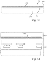
FIG. 1c , a silicon-on-insulator arrangement 110 comprising asilicon wafer 112, a buriedoxide 114, and asilicon layer 116, is illustrated. A step of implantation and annealing of thesilicon layer 116 may be performed. The dopant type and density may preferably be chosen according to application type of the fluid sensor device. Anative oxide 118 may be present at the surface of thesilicon layer 116. Thenative oxide 118 may enable a fusion bonding process with the planarized dielectric layer of the CMOS arrangement. Alternatively or additionally, athin dielectric layer 118 may be deposited on thesilicon layer 116 in order to protect thesilicon layer 116 and/or in order to enable the fusion bonding process. - It is envisioned that a forming of a fin-FET arrangement in the
silicon layer 116 may be performed prior to bonding of the silicon-on-insulator arrangement 110 to the CMOS arrangement. Such a step of forming may comprise patterning of thesilicon layer 116. By forming the fin-FET arrangement in thesilicon layer 116 prior to bonding of the silicon-on-insulator arrangement 110 to the CMOS arrangement, it is possible to utilize processes which would otherwise have damaged or degraded the CMOS arrangement. Hereby, a high resolution fin-FET arrangement may be achieved. - In the embodiment illustrated in
FIGS. 1a - 1p , the forming of the fin-FET arrangement in thesilicon layer 116 is performed after bonding of the silicon-on-insulator arrangement 110 to the CMOS arrangement. - Referring now to
FIG. 1d , the silicon-on-insulator arrangement 110 has been bonded to theCMOS arrangement 102. As can be seen, the silicon-on-insulator arrangement 110 is oriented such that thesilicon layer 116 is closer to theCMOS arrangement 102 than thesilicon wafer 114. - Referring now to
FIG. 1e , the silicon wafer and buried oxide of the silicon-on-insulator arrangement has been removed. The removal may be performed by grinding or similar processes. Thesilicon layer 116 is left on top of theCMOS arrangement 102. - Referring now to
FIG. 1f , a forming of a fin-FET arrangement 120 in thesilicon layer 116 has been performed. The fin-FET arrangement 120 may comprise several fin-FETs, which may respectively be arranged between a source and a drain of a transistor in the fin-FET arrangement 120. It should also be realized that a plurality of transistors comprising source, drain and fin-FETs therebetween may be formed in the fin-FET arrangement 120. - Referring now to
FIG. 1g , anetch stop layer 122 has been formed over the fin-FET arrangement 120. Theetch stop layer 122 may be formed via deposition. Theetch stop layer 122 may protect the underlying structures from being etched in the subsequent manufacturing of the fluid sensing device. In particular, theetch stop layer 122 may protect the fin-FET arrangement 120 from an etch process. Further, theetch stop layer 122 may protect the fin-FET arrangement 120 from substances, e.g. sodium, present in a fluid intended to be analyzed by the fluid sensor device. Theetch stop layer 122 may also serve as a gate dielectric and/or as a base layer for bio functionalization purposes. - Referring now to
FIG. 1h , asecond dielectric layer 124 has been formed over the fin-FET arrangement 120. Thesecond dielectric layer 124 may fill gaps present in the fin-FET arrangement 120, and in particular between individual fin-FETs of the fin-FET arrangement 120. The second dielectric layer may protect the fin-FETs in processing to form connections between the fin-FET arrangement 120 and theCMOS arrangement 102. - Referring now to
FIG. 1i , a portion of the planarizeddielectric layer 108 and thesecond dielectric layer 124 has been removed. Such a removal may be performed via a lithography process, which may include one or more lithography steps. The removal of a portion of the planarizeddielectric layer 108 and thesecond dielectric layer 124 may expose a portion of themetallization layer 104 and a portion of the fin-FET arrangement 120. - Referring now to
FIG. 1j , acontact 126 to themetallization layer 104 and the fin-FET arrangement 120 has been formed. Thecontact 126 may be at least partially enclosed by the planarizeddielectric layer 108 and thesecond dielectric layer 124. Here, thecontact 126 comprises a vertical arrangement comprising a firstvertical portion 128 and a secondvertical portion 130. The firstvertical portion 128 is configured to be in contact with the fin-FET arrangement 120, and the secondvertical portion 130 is configured to be in contact with themetallization layer 104. - Still referring to
FIG. 1j , a planarization is also illustrated. Such a planarization may be performed in order to remove excess material from the formation of thecontact 126. Further, the planarization may also serve to separate the firstvertical portion 128 from the secondvertical portion 130. This may facilitate a formation of an interconnecting structure configured to interconnect themetallization layer 104 and the fin-FET arrangement 120. In particular, the interconnecting structure may be configured to interconnect themetallization layer 104 and the fin-FET arrangement 120 via the first and secondvertical portions - Referring now to
FIG. 1k , an interconnectingstructure 132 of thecontact 126 has been formed. The interconnectingstructure 132 may comprise a material being different from the first and second vertical portions 128,130. - Referring now to
FIG. 1L , a thirddielectric layer 134 has been formed over the fin-FET arrangement 120. In particular, the thirddielectric layer 134 may be formed on the interconnectingstructure 132 and thesecond dielectric layer 124. The thirddielectric layer 134 may be planarized subsequent to formation. The thirddielectric layer 134 may provide a top dielectric layer to which a microfluidic arrangement may be bonded. Further, the second and/or thirddielectric layer FET arrangement 120. Such a channel may be formed by removing a portion of the second and/or thirddielectric layer dielectric layer FET arrangement 120. - Referring now to
FIG. 1m , a portion of the second and thirddielectric layers etch stop layer 122 may provide for that the fin-FET arrangement 120 and/or any dielectric present under the fin-FET arrangement 120 are protected during removal of the portion of the second and thirddielectric layers - Referring now to
FIG. 1n , the etch stop layer has been removed. This may be done in order to form a freshmetal oxide layer 136 as illustrated inFIG. 1o over the fin-FET arrangement 120. Themetal oxide layer 136 may also be formed on the thirddielectric layer 134. As can be seen, themetal oxide layer 136 may also cover aside portion 137 of the second and/or thirddielectric layer metal oxide layer 136 may comprise AlO, HfO, SiO or similar materials. - Referring now to
FIG. 1p , a portion of the interconnectingstructure 132 has been exposed in order to form abond pad opening 138. The bond pad opening may provide for that the fluid sensor device can be connected to other devices. The bond pad opening 138 may also provide for that a signal from the fin-FET arrangement can be received by another device. - Referring now to
FIG. 1q , amicrofluidic arrangement 140 has been bonded to the thirddielectric layer 134. The bonding may be performed by fusion bonding. Here, themicrofluidic arrangement 140 together with thesecond dielectric layer 124 and thirddielectric layer 134 forms part of thechannel 142. Thechannel 142 comprises aninlet 144 and anoutlet 146. Thechannel 142 is configured to at least partially expose the fin-FET arrangement 120 and to allow a fluid comprising an analyte to contact the fin-FET arrangement 120. - Thus, in
FIG. 1q , afluid sensor device 100 is shown, having a fin-FET arrangement 120 over aCMOS arrangement 102, wherein an interconnectingstructure 132 interconnects themetallization layer 104 of theCMOS arrangement 102 with the fin-FET arrangement 120. The fin-FET arrangement 120 is at least partially exposed in thechannel 142. - The
microfluidic arrangement 140 may comprise various microfluidic structures, e.g. amicrofluidic structure 146 configured to facilitate the analysis of the fluid by thefluid sensor device 100. The various microfluidic structures may add additional functionality to thefluid sensor device 100. Examples of such structures include e.g. valves, filters, lysing elements, and structures configured to dilute a fluid comprising an analyte, wherein the fluid is intended to be analyzed by thefluid sensor device 100. In general, themicrofluidic arrangement 140 may be configured to treat the fluid comprising the analyte, wherein the fluid is intended to contact the fin-FET arrangement 120. Themicrofluidic arrangement 140 may comprise anopening 148 configured to align with thebond pad opening 138. - The
fluid sensor device 100 may be configured to allow selective contacting of an analyte to the fin-FETs of the fin-FET arrangement 120. The analyte may change a charge of the gate of the fin-FET arrangement 120 when forming a contact with the fin-FETs such that a conductance in the fin-FETs is changed. This may cause a current to flow from source to drain in the transistor formed by the fin-FET arrangement 120 such that a fluid sensor signal may be generated, which may be transferred to theCMOS arrangement 102 for further processing, such as amplifying of the signal. - The set-up of using fin-FETs to which analytes may form contact or be attached may be very sensitive. In an embodiment, the
fluid sensor device 100 may allow sensing of a single molecule attaching to the fin-FETs. - The analyte may be any kind of substance in the fluid, such as a biological substance, e.g. a DNA or RNA string. The fluid may be liquid or gaseous, allowing sensing of analytes in a liquid or a gas.
- In the above the inventive concept has mainly been described with reference to a limited number of examples. However, as is readily appreciated by a person skilled in the art, other examples than the ones disclosed above are equally possible within the scope of the inventive concept, as defined by the appended claims.
Claims (15)
- A method for manufacturing a fluid sensor device, the method comprising:bonding a silicon-on-insulator arrangement comprising a silicon wafer, a buried oxide, a silicon layer, and a first dielectric layer, to a CMOS arrangement comprising a metallization layer and a planarized dielectric layer, wherein the bonding is performed via the first dielectric layer and the planarized dielectric layer;forming a fin-FET arrangement in the silicon layer, wherein the fin-FET arrangement is configured to function as a fluid sensitive fin-FET arrangement;removing the buried oxide and the silicon wafer;forming a contact to the metallization layer and the fin-FET arrangement, wherein the contact comprises an interconnecting structure configured to interconnect the metallization layer and the fin-FET arrangement;forming a channel comprising an inlet and an outlet, wherein the channel is configured to at least partially expose the fin-FET arrangement and to allow a fluid comprising an analyte to contact the fin-FET arrangement.
- The method according to claim 1, wherein the CMOS arrangement comprises an amplifying structure configured to amplify a signal from the fin-FET arrangement.
- The method according to claim 2, wherein the metallization layer is configured to provide contact to the amplifying structure of the CMOS arrangement.
- The method according to any one of the preceding claims, further comprising forming a second dielectric layer over the fin-FET arrangement, and wherein the contact to the metallization layer and the fin-FET arrangement is configured to be at least partially enclosed by the planarized dielectric layer and the second dielectric layer.
- The method according to any one of the preceding claims, further comprising forming a third dielectric layer over the contact and the fin-FET arrangement.
- The method according to claims 4 and 5, wherein the step of forming the channel comprises removing a portion of the second and third dielectric layer, and bonding a microfluidic arrangement to the third dielectric layer.
- The method according to any one of the preceding claims, wherein the contact comprises a vertical arrangement comprising a first vertical portion configured to be in contact with the fin-FET arrangement, and a second vertical portion configured to be in contact with the metallization layer, wherein the interconnecting structure is configured to connect the metallization layer and the fin-FET arrangement via the vertical arrangement.
- The method according to anyone of the preceding claims, further comprising forming an etch stop layer over the fin-FET arrangement prior to the step of forming the contact to the metallization layer and the fin-FET arrangement.
- The method according to claim 8, wherein the etch stop layer comprises a material selected from the group consisting of SiN, metal oxides, and metal.
- The method according to claim 8 or 9, wherein the etch stop layer is at least partially removed in conjunction with forming the channel, and wherein a metal oxide layer is thereafter formed over the fin-FET arrangement.
- The method according to any one of the preceding claims, wherein the step of forming a fin-FET arrangement in the silicon layer is performed prior to the step of bonding the silicon-on-insulator arrangement to the CMOS arrangement.
- The method according to any one of the preceding claims, wherein the step of forming a fin-FET arrangement in the silicon layer is performed after the step of bonding the silicon-on-insulator arrangement to the CMOS arrangement, and after the step of removing the buried oxide and the silicon wafer.
- The method according to any one of the preceding claims, wherein the fin-FET arrangement comprises nanopore fin-FETs.
- The method according to any one of the preceding claims, wherein a portion of the interconnecting structure is exposed in order to form a bond pad opening.
- A fluid sensor device comprising:a CMOS arrangement comprising a metallization layer;a fin-FET arrangement configured to function as a fluid sensitive fin-FET arrangement and to generate a fluid sensor signal, wherein the fin-FET arrangement is arranged over the CMOS arrangement;a contact to the metallization layer and the fin-FET arrangement, wherein the contact comprises an interconnecting structure configured to interconnect the metallization layer and the fin-FET arrangement;wherein the fin-FET arrangement is configured to transfer the fluid sensor signal to the CMOS arrangement via the interconnecting structure, and wherein the CMOS arrangement is configured to process the fluid sensor signal;and wherein the fluid sensor device further comprisesa channel comprising an inlet and an outlet, wherein the fin-FET arrangement is configured to be at least partially exposed in the channel to allow a fluid comprising an analyte to contact the fin-FET arrangement.
Priority Applications (4)
| Application Number | Priority Date | Filing Date | Title |
|---|---|---|---|
| EP17210420.0A EP3502682A1 (en) | 2017-12-22 | 2017-12-22 | A method for manufacturing a fluid sensor device and a fluid sensor device |
| US16/957,090 US11676851B2 (en) | 2017-12-22 | 2018-12-19 | Method for manufacturing a fluid sensor device and a fluid sensor device |
| PCT/EP2018/085864 WO2019121931A1 (en) | 2017-12-22 | 2018-12-19 | A method for manufacturing a fluid sensor device and a fluid sensor device |
| EP18836232.1A EP3729068B1 (en) | 2017-12-22 | 2018-12-19 | A method for manufacturing a fluid sensor device and a fluid sensor device |
Applications Claiming Priority (1)
| Application Number | Priority Date | Filing Date | Title |
|---|---|---|---|
| EP17210420.0A EP3502682A1 (en) | 2017-12-22 | 2017-12-22 | A method for manufacturing a fluid sensor device and a fluid sensor device |
Publications (1)
| Publication Number | Publication Date |
|---|---|
| EP3502682A1 true EP3502682A1 (en) | 2019-06-26 |
Family
ID=60937570
Family Applications (2)
| Application Number | Title | Priority Date | Filing Date |
|---|---|---|---|
| EP17210420.0A Withdrawn EP3502682A1 (en) | 2017-12-22 | 2017-12-22 | A method for manufacturing a fluid sensor device and a fluid sensor device |
| EP18836232.1A Active EP3729068B1 (en) | 2017-12-22 | 2018-12-19 | A method for manufacturing a fluid sensor device and a fluid sensor device |
Family Applications After (1)
| Application Number | Title | Priority Date | Filing Date |
|---|---|---|---|
| EP18836232.1A Active EP3729068B1 (en) | 2017-12-22 | 2018-12-19 | A method for manufacturing a fluid sensor device and a fluid sensor device |
Country Status (3)
| Country | Link |
|---|---|
| US (1) | US11676851B2 (en) |
| EP (2) | EP3502682A1 (en) |
| WO (1) | WO2019121931A1 (en) |
Families Citing this family (3)
| Publication number | Priority date | Publication date | Assignee | Title |
|---|---|---|---|---|
| US12601710B2 (en) * | 2022-11-15 | 2026-04-14 | Globalfoundries U.S. Inc. | Ion-sensitive field-effect transistors with local-field bias |
| TWI869136B (en) * | 2022-12-22 | 2025-01-01 | 國立臺灣大學 | Semiconductor chip with embedded microfluidic channels and method of fabricating the same |
| DE102023202135B9 (en) | 2023-03-09 | 2025-07-24 | Carl Zeiss Smt Gmbh | Sensor arrangement for arrangement on a measuring chamber, device for qualifying a mask and method for qualifying a mask |
Citations (4)
| Publication number | Priority date | Publication date | Assignee | Title |
|---|---|---|---|---|
| DE10254158A1 (en) * | 2002-11-20 | 2004-06-09 | Infineon Technologies Ag | Sensor system for detecting signals from biological cells comprises semiconductor substrate containing field effect transistor whose channel has coupling component connecting it to sensor surface |
| US20100066348A1 (en) * | 2007-04-25 | 2010-03-18 | Nxp B.V. | Apparatus and method for molecule detection using nanopores |
| US20120161333A1 (en) * | 2010-12-23 | 2012-06-28 | Commissariat A L'energie Atomique Et Aux Ene Alt | Device for connecting nano-objects to external electrical systems, and method for producing said device |
| US20150268189A1 (en) * | 2014-03-19 | 2015-09-24 | Ecole Polytechnique Federale De Lausanne (Epfl) | Method to fabricate finfet sensors, in particular, finfet sensors for ionic, chemical and biological applications on si-bulk |
Family Cites Families (7)
| Publication number | Priority date | Publication date | Assignee | Title |
|---|---|---|---|---|
| US6242324B1 (en) * | 1999-08-10 | 2001-06-05 | The United States Of America As Represented By The Secretary Of The Navy | Method for fabricating singe crystal materials over CMOS devices |
| US8513791B2 (en) * | 2007-05-18 | 2013-08-20 | International Business Machines Corporation | Compact multi-port CAM cell implemented in 3D vertical integration |
| KR100940524B1 (en) * | 2007-12-13 | 2010-02-10 | 한국전자통신연구원 | High Sensitivity Semiconductor FET Sensor and Manufacturing Method Thereof |
| US9134270B2 (en) * | 2010-03-25 | 2015-09-15 | Stichting Imec Nederland | Amorphous thin film for sensing |
| CN103842817A (en) | 2010-09-29 | 2014-06-04 | 得克萨斯系统大学评议会 | Fin-FET biosensor with improved sensitivity and specificity |
| US10006910B2 (en) * | 2014-12-18 | 2018-06-26 | Agilome, Inc. | Chemically-sensitive field effect transistors, systems, and methods for manufacturing and using the same |
| US10048220B2 (en) * | 2015-10-08 | 2018-08-14 | Taiwan Semiconductor Manufacturing Company Ltd. | Biosensor field effect transistor having specific well structure and method of forming the same |
-
2017
- 2017-12-22 EP EP17210420.0A patent/EP3502682A1/en not_active Withdrawn
-
2018
- 2018-12-19 US US16/957,090 patent/US11676851B2/en active Active
- 2018-12-19 EP EP18836232.1A patent/EP3729068B1/en active Active
- 2018-12-19 WO PCT/EP2018/085864 patent/WO2019121931A1/en not_active Ceased
Patent Citations (4)
| Publication number | Priority date | Publication date | Assignee | Title |
|---|---|---|---|---|
| DE10254158A1 (en) * | 2002-11-20 | 2004-06-09 | Infineon Technologies Ag | Sensor system for detecting signals from biological cells comprises semiconductor substrate containing field effect transistor whose channel has coupling component connecting it to sensor surface |
| US20100066348A1 (en) * | 2007-04-25 | 2010-03-18 | Nxp B.V. | Apparatus and method for molecule detection using nanopores |
| US20120161333A1 (en) * | 2010-12-23 | 2012-06-28 | Commissariat A L'energie Atomique Et Aux Ene Alt | Device for connecting nano-objects to external electrical systems, and method for producing said device |
| US20150268189A1 (en) * | 2014-03-19 | 2015-09-24 | Ecole Polytechnique Federale De Lausanne (Epfl) | Method to fabricate finfet sensors, in particular, finfet sensors for ionic, chemical and biological applications on si-bulk |
Non-Patent Citations (4)
| Title |
|---|
| M. SENGUPTA ET AL: "Effects of Rapid Thermal Annealing Temperature on Performances of Nanoscale FinFETs", JSTS:JOURNAL OF SEMICONDUCTOR TECHNOLOGY AND SCIENCE, vol. 9, no. 4, 30 December 2009 (2009-12-30), pages 266 - 272, XP055472188, ISSN: 1598-1657, DOI: 10.5573/JSTS.2009.9.4.266 * |
| MOHTASHIM MANSOOR ET AL: "An SOI CMOS-Based Multi-Sensor MEMS Chip for Fluidic Applications", SENSORS, vol. 16, no. 11, 4 November 2016 (2016-11-04), pages 1608, XP055411629, DOI: 10.3390/s16111608 * |
| RIGANTE S ET AL: "Low power finfet ph-sensor with high-sensitivity voltage readout", 2013 PROCEEDINGS OF THE EUROPEAN SOLID-STATE DEVICE RESEARCH CONFERENCE (ESSDERC), IEEE, 16 September 2013 (2013-09-16), pages 350 - 353, XP032596950, DOI: 10.1109/ESSDERC.2013.6818890 * |
| TAKEUCHI H ET AL: "Thermal Budget Limits of Quarter-Micrometer Foundry CMOS for Post-Processing MEMS Devices", IEEE TRANSACTIONS ON ELECTRON DEVICES, IEEE SERVICE CENTER, PISACATAWAY, NJ, US, vol. 52, no. 9, 2 September 2005 (2005-09-02), pages 2081 - 2086, XP011138322, ISSN: 0018-9383, DOI: 10.1109/TED.2005.854287 * |
Also Published As
| Publication number | Publication date |
|---|---|
| EP3729068B1 (en) | 2022-11-16 |
| EP3729068A1 (en) | 2020-10-28 |
| US11676851B2 (en) | 2023-06-13 |
| WO2019121931A1 (en) | 2019-06-27 |
| US20200350200A1 (en) | 2020-11-05 |
Similar Documents
| Publication | Publication Date | Title |
|---|---|---|
| US12216077B2 (en) | BioFET device having a metal crown structure as a sensing layer disposed on an oxide layer formed under a channel region of a transistor | |
| US10184912B2 (en) | Backside sensing BioFET with enhanced performance | |
| US12529675B2 (en) | CMOS compatible BioFET | |
| US11099152B2 (en) | Backside CMOS compatible BioFET with no plasma induced damage | |
| TWI807249B (en) | Biosensor system package and method for fabricating the same | |
| US10101295B2 (en) | On-chip reference electrode for biologically sensitive field effect transistor | |
| US9395326B2 (en) | FET sensing cell and method of improving sensitivity of the same | |
| TW201721873A (en) | Semiconductor device and method of manufacturing the same | |
| US11676851B2 (en) | Method for manufacturing a fluid sensor device and a fluid sensor device | |
| WO2008068692A1 (en) | Method of manufacturing a semiconductor sensor device and semiconductor sensor device obtained with such method |
Legal Events
| Date | Code | Title | Description |
|---|---|---|---|
| PUAI | Public reference made under article 153(3) epc to a published international application that has entered the european phase |
Free format text: ORIGINAL CODE: 0009012 |
|
| STAA | Information on the status of an ep patent application or granted ep patent |
Free format text: STATUS: THE APPLICATION HAS BEEN PUBLISHED |
|
| AK | Designated contracting states |
Kind code of ref document: A1 Designated state(s): AL AT BE BG CH CY CZ DE DK EE ES FI FR GB GR HR HU IE IS IT LI LT LU LV MC MK MT NL NO PL PT RO RS SE SI SK SM TR |
|
| AX | Request for extension of the european patent |
Extension state: BA ME |
|
| STAA | Information on the status of an ep patent application or granted ep patent |
Free format text: STATUS: THE APPLICATION IS DEEMED TO BE WITHDRAWN |
|
| 18D | Application deemed to be withdrawn |
Effective date: 20200103 |