EP3502665A1 - Devices and methods for total internal reflection (tir) microscopy - Google Patents
Devices and methods for total internal reflection (tir) microscopy Download PDFInfo
- Publication number
- EP3502665A1 EP3502665A1 EP17306916.2A EP17306916A EP3502665A1 EP 3502665 A1 EP3502665 A1 EP 3502665A1 EP 17306916 A EP17306916 A EP 17306916A EP 3502665 A1 EP3502665 A1 EP 3502665A1
- Authority
- EP
- European Patent Office
- Prior art keywords
- sample
- electromagnetic field
- illumination
- interface
- illumination beam
- Prior art date
- Legal status (The legal status is an assumption and is not a legal conclusion. Google has not performed a legal analysis and makes no representation as to the accuracy of the status listed.)
- Withdrawn
Links
- 238000000386 microscopy Methods 0.000 title claims abstract description 47
- 238000000034 method Methods 0.000 title claims description 53
- 238000005286 illumination Methods 0.000 claims abstract description 132
- 230000005672 electromagnetic field Effects 0.000 claims abstract description 92
- 230000003287 optical effect Effects 0.000 claims abstract description 34
- 238000001514 detection method Methods 0.000 claims abstract description 29
- 230000001427 coherent effect Effects 0.000 claims abstract description 10
- 238000002310 reflectometry Methods 0.000 claims description 20
- 238000001914 filtration Methods 0.000 claims description 5
- 230000000903 blocking effect Effects 0.000 claims description 4
- 230000002123 temporal effect Effects 0.000 claims description 3
- 239000000523 sample Substances 0.000 description 95
- 238000013459 approach Methods 0.000 description 9
- 238000007654 immersion Methods 0.000 description 8
- 239000000758 substrate Substances 0.000 description 7
- 230000004075 alteration Effects 0.000 description 6
- 239000011521 glass Substances 0.000 description 6
- 238000005259 measurement Methods 0.000 description 6
- 230000008901 benefit Effects 0.000 description 5
- 238000001093 holography Methods 0.000 description 5
- 239000007788 liquid Substances 0.000 description 5
- 238000011282 treatment Methods 0.000 description 5
- 210000004027 cell Anatomy 0.000 description 4
- 238000000799 fluorescence microscopy Methods 0.000 description 4
- 238000003384 imaging method Methods 0.000 description 4
- 210000001747 pupil Anatomy 0.000 description 4
- 239000011347 resin Substances 0.000 description 4
- 229920005989 resin Polymers 0.000 description 4
- 238000000492 total internal reflection fluorescence microscopy Methods 0.000 description 4
- 238000000204 total internal reflection microscopy Methods 0.000 description 4
- 241000961787 Josa Species 0.000 description 3
- 230000010287 polarization Effects 0.000 description 3
- XLYOFNOQVPJJNP-UHFFFAOYSA-N water Substances O XLYOFNOQVPJJNP-UHFFFAOYSA-N 0.000 description 3
- 239000012472 biological sample Substances 0.000 description 2
- 238000012512 characterization method Methods 0.000 description 2
- 238000013500 data storage Methods 0.000 description 2
- 239000012528 membrane Substances 0.000 description 2
- 238000001000 micrograph Methods 0.000 description 2
- 238000012986 modification Methods 0.000 description 2
- 230000004048 modification Effects 0.000 description 2
- 239000002086 nanomaterial Substances 0.000 description 2
- 238000010606 normalization Methods 0.000 description 2
- 238000000926 separation method Methods 0.000 description 2
- 238000000018 DNA microarray Methods 0.000 description 1
- 206010034972 Photosensitivity reaction Diseases 0.000 description 1
- 238000004061 bleaching Methods 0.000 description 1
- 210000000170 cell membrane Anatomy 0.000 description 1
- 230000021615 conjugation Effects 0.000 description 1
- 239000002872 contrast media Substances 0.000 description 1
- 238000012217 deletion Methods 0.000 description 1
- 230000037430 deletion Effects 0.000 description 1
- 239000000835 fiber Substances 0.000 description 1
- 239000007850 fluorescent dye Substances 0.000 description 1
- 230000006870 function Effects 0.000 description 1
- 238000012615 high-resolution technique Methods 0.000 description 1
- 238000011503 in vivo imaging Methods 0.000 description 1
- 230000010354 integration Effects 0.000 description 1
- 238000002372 labelling Methods 0.000 description 1
- 238000010859 live-cell imaging Methods 0.000 description 1
- 230000007774 longterm Effects 0.000 description 1
- 238000012634 optical imaging Methods 0.000 description 1
- 230000008520 organization Effects 0.000 description 1
- 230000010363 phase shift Effects 0.000 description 1
- 208000007578 phototoxic dermatitis Diseases 0.000 description 1
- 231100000018 phototoxicity Toxicity 0.000 description 1
- 230000008569 process Effects 0.000 description 1
- 238000012545 processing Methods 0.000 description 1
- 230000000750 progressive effect Effects 0.000 description 1
- 230000001902 propagating effect Effects 0.000 description 1
- 230000035945 sensitivity Effects 0.000 description 1
- 230000003595 spectral effect Effects 0.000 description 1
- 238000003325 tomography Methods 0.000 description 1
- 238000013519 translation Methods 0.000 description 1
- 238000012800 visualization Methods 0.000 description 1
Images




Classifications
-
- G—PHYSICS
- G01—MEASURING; TESTING
- G01N—INVESTIGATING OR ANALYSING MATERIALS BY DETERMINING THEIR CHEMICAL OR PHYSICAL PROPERTIES
- G01N21/00—Investigating or analysing materials by the use of optical means, i.e. using sub-millimetre waves, infrared, visible or ultraviolet light
- G01N21/17—Systems in which incident light is modified in accordance with the properties of the material investigated
- G01N21/55—Specular reflectivity
- G01N21/552—Attenuated total reflection
-
- G—PHYSICS
- G01—MEASURING; TESTING
- G01N—INVESTIGATING OR ANALYSING MATERIALS BY DETERMINING THEIR CHEMICAL OR PHYSICAL PROPERTIES
- G01N21/00—Investigating or analysing materials by the use of optical means, i.e. using sub-millimetre waves, infrared, visible or ultraviolet light
- G01N21/17—Systems in which incident light is modified in accordance with the properties of the material investigated
- G01N21/41—Refractivity; Phase-affecting properties, e.g. optical path length
- G01N21/45—Refractivity; Phase-affecting properties, e.g. optical path length using interferometric methods; using Schlieren methods
- G01N21/453—Holographic interferometry
Definitions
- the present description relates to devices and methods for total internal reflection microscopy, and applies in particular to label-free optical imaging of samples.
- Total internal reflection fluorescence (TIRF) microscopy is a reference technique to study the membrane dynamics and organization in biological cells ( See for example D. Axelrod et al., "Cell-substrate contacts illuminated by total internal reflection fluorescence", The Journal of cell biolology 89, 141 (1981 )). Its main advantage is the ability to illuminate the sample over a thin slice of about 100 nm, by taking benefit from a total internal reflection (TIR) configuration.
- TIR total internal reflection
- a sample S is deposited on a cover slip 10, for example a glass substrate, and by illuminating through the substrate above the critical angle (illumination beam 11), an evanescent wave 12 is created at the interface to locally probe the sample.
- a high numerical aperture immersion objective 13 is used, to both illuminate above the critical angle and collect the fluorescence signal 14. Compared to standard wide field fluorescence microscopy, images with highly improved contrast are provided, since the background signal stemming from the volume of the sample can be suppressed.
- fluorophores as contrast agents however presents some drawbacks, as their addition is invasive and induces the increased risk of photo bleaching and photo toxicity to the cell. Long-term studies are therefore difficult to achieve.
- specificity of labeling prevents the visualization of the whole sample; it is therefore at the same time the main advantage and the main limitation of fluorescence imaging. As a result, there is a need for a high resolution technique able to probe cell membranes without the constraint of incorporating a fluorescent label.
- TIR total internal reflection
- the spatial resolution is limited to the Rayleigh criterion (0.6 ⁇ m /NA, where ⁇ m is the average wavelength of illumination and NA the numerical aperture of the objective), and the method amounts to considering the sample as a succession of planar diopters placed at different heights. This method is thus preferably adopted for samples having soft and progressive profiles of height.
- the second approach uses a laser beam focused in the back focal plane (BFP) of the objective at the edge of the numerical aperture (see for example F. Jünger et al., "Fast, label-free super-resolution live-cell imaging using rotating coherent scattering (ROCS) microscopy", Scientific reports 6, 30393 ).
- the focused beam is scanned along a circle in the BFP, so that the sample is illuminated in TIR by a rotating collimated beam, and the integration time of the camera is set to match the rotation period of the beam.
- the totally reflected beam is blocked in a plane conjugated with the BFP to detect only the scattered intensity and obtain dark field imaging.
- this method claims a good spatial resolution (slightly better than the Rayleigh criterion), it is principally used for qualitative measurements as it is known to slightly distort the image compared to the object.
- the present invention proposes a new method for total internal reflection microscopy, which can provide with a simple arrangement the phase of the signal backscattered by the sample and further improves the imaging spatial resolution compared to the previous approaches.
- the present description relates to a device for TIR microscopy of a sample comprising:
- the device for TIR microscopy as described above enables a label-free TIR microscopy technique, which keeps the same set-up simplicity as the previous approaches for TIR microscopy but also permits to perform phase imaging.
- an off-axis holography scheme is provided but without the need of any external reference wave.
- said at least one map (or "image") of a physical parameter related to the sample comprises at least one of: a 2D map of the phase and/or modulus of said first backscattered signal electromagnetic field, a 2D map of the real part and/or imaginary part and/or modulus and/or phase of an equivalent reflectivity r eq of the sample, a 3D map of the real and/or imaginary parts of a permittivity contrast ⁇ of the sample.
- the permittivity contrast ⁇ may be defined as the difference between the relative dielectric permittivity of the object (the square of the refractive index) and that of the background.
- said illumination path further comprises scanning means for controlling said azimuth angle and/or said polar angle of at least said first illumination beam.
- the scanning means comprise at least a first axis of rotation situated in a plane optically conjugated with said interface between the sample and the support.
- the scanning means are configured to form a temporal sequence of illumination beams, including said first illumination beam, and having different azimuth and/or polar angles adapted for total internal reflection at said interface, each illumination beam thus forming an evanescent electromagnetic field in the sample;
- the first detection path is configured for the acquisition of a plurality of interferograms, each interferogram resulting from the optical interference between at least one reference electromagnetic field and at least one backscattered signal electromagnetic field, wherein said reference electromagnetic field results from the total internal reflection of one of said illumination beams at said interface and said backscattered signal electromagnetic field results from the scattering by the sample of said evanescent electromagnetic field formed by said illumination beam;
- the computing device is configured to compute said at least one map of a physical parameter related to the sample from said plurality of interferograms.
- the resolution is defined by the smallest distance between two points of the object that can be distinguished through the microscope objective.
- the device for TIR microscopy further comprises a second detection path, wherein said second detection path comprises said microscope objective, a second bidimensional optical acquisition device for acquisition of a fluorescence signal resulting from the fluorescence of said sample and a beam splitter configured to direct said fluorescence signal to said second bidimensional optical acquisition device.
- said illumination path further comprises a beam shaper element adapted to form simultaneously said first illumination beam and a second illumination beam, wherein the first and second illumination beams have the same polar angle and two azimuth angles spaced by 180°.
- said first acquisition path further comprises a spatial filter for blocking one of the first and second reflections beams, resulting respectively from the total internal reflection of said first and second illumination beams at said interface between the sample and the support.
- the present description relates to a method for TIR microscopy of a sample comprising the steps of:
- the computing step comprises performing a numerical 2D Fourier transform of said at least first interferogram and filtering said 2D Fourier transform to retrieve the 2D Fourier transform of said first backscattered signal electromagnetic field. It is thus possible to retrieve a 2D map of the phase and/or modulus of said first backscattered signal electromagnetic field.
- the illuminating step comprises sequentially illuminating said interface with a plurality of illumination beams, including said first illumination beam and having different azimuth angles and polar angles adapted for total internal reflection at said interface, each illumination beam thus forming an evanescent electromagnetic field in the sample;
- the detecting step comprises acquiring a plurality of interferograms, each interferogram resulting from the optical interference between at least one reference electromagnetic field and at least one backscattered signal electromagnetic field, wherein said reference electromagnetic field results from the total internal reflection of one of said illumination beams at said interface and said backscattered signal electromagnetic field results from the scattering by the sample of an evanescent electromagnetic field formed by said illumination beam in the sample;
- the computing step comprises computing, from said plurality of interferograms, at least one map of a physical parameter related to the sample.
- Said at least one map of a physical parameter related to the sample may comprise at least one of: a 2D map of the phase and/or modulus of a backscattered signal electromagnetic field resulting from the scattering by the sample of the evanescent electromagnetic field formed by any of the illumination beams, a 2D map of an equivalent reflectivity r eq of the sample, a 3D map of permittivity contrast ⁇ of the sample.
- a 2D map of an equivalent reflectivity r eq of the sample, or a 3D map of permittivity contrast ⁇ of the sample may be retrieved from one or a plurality of said 2D maps of backscattered signal electromagnetic fields, or directly from one or a plurality of said interferograms.
- the computing step comprises performing a summation of said plurality of interferograms. It is thus possible to directly retrieve a 2D map of the real part of an equivalent reflectivity r eq of the sample.
- the computing step comprises:
- the computing step further comprises normalizing the 2D Fourier transform of the backscattered signal electromagnetic field for each illumination angle before summing, to correct from a phase and/or modulus mismatch between the different backscattered signal electromagnetic fields in the Fourier domain.
- the method for TIR microscopy further comprises acquiring using a second detection path, a fluorescence signal resulting from the fluorescence of the sample.
- the illuminating step comprises simultaneously illuminating said interface with said first illumination beam and a second illumination beam, wherein the first and second illumination beams have the same polar angle and two azimuth angles spaced by 180°.
- the detecting step further comprises blocking one of the first and second reflections beams, resulting respectively from the total internal reflection of said first and second illumination beams at said interface between the sample and the support.
- FIG. 2A is a schematic view of an exemplary architecture of a device 200 for TIR microscopy of a sample in an EPI configuration for detecting the total internal reflection.
- the device 200 includes a support 210 for receiving the sample.
- a detailed view of an interface 211 between the support and the sample is shown in FIG. 2C .
- the support is for example made of glass, or any transparent medium which permits to generate total internal reflection at interface 211.
- the sample may be any object in a surrounding medium (e.g. liquids or air), i.e.any micro or nanostructure having a refractive index is different from that of the medium.
- the sample may be a biological sample in solution, or a micro or nanostructure directly deposited on the support, e.g. biochips.
- a low refractive index difference between the object and the medium e.g. ⁇ n ⁇ 0.5, will provide a better performance of the measurements, as the field backscattered by the object will be weak compared to the total internal reflection.
- the device 200 for TIR microscopy further includes an illumination path of the sample comprising a spatially coherent light source 220 and a microscope objective 230 with a back focal plane (BFP) 231, also referred to as the Fourier plane.
- the illumination path is configured to form at least a first illumination beam I 1 for illuminating the interface 211 between the support 210 and the sample S.
- the spatial coherent source 220 is for example a laser source, a laser diode or any light source where light is sufficiently spatially filtered (through a pinhole, a monomode fiber...) so that each illumination angle through microscope objective 230 is defined with a typical angle variation in radians of ⁇ m /(10D), where ⁇ m is the average wavelength of the illumination beam and D is the maximal diameter of the sample.
- the beam I 0 emitted by the source 220 may be a linearly polarized laser beam, in which case the illumination path may further comprise a wave plate 221, for example a motorized wave plate, adapted to adjust the polarization direction of the laser beam I 0 .
- a wave plate 221 for example a motorized wave plate, adapted to adjust the polarization direction of the laser beam I 0 .
- the illumination path further comprises scanning means 222 to control the polar angle and azimuth angle of the illumination beam and a beam expander 223 for generating a wide collimated beam.
- the illumination path further comprises a beam splitter 224 to direct the collimated beam towards the microscope objective 230 and a tube lens 225, whose front focal plane is superposed with the back focal plane 231 of the objective.
- At least a first collimated illumination beam I 1 is thus generated at the exit of the microscope objective 230, wherein said illumination beam I 1 is impinging on the interface between the sample and the support (plane xOy in FIG. 2B ) with a first azimuth angle ⁇ 1 and a first polar angle (or tilt angle) ⁇ 1 .
- the polar angle ⁇ 1 is adapted for total internal reflection of the first illumination beam I 1 at the interface 211 between the support and the sample.
- Scanning means 222 may comprise a rotary optic, for example a combination of galvanometric systems or a combination of MEMS mirrors (with one axis) or one MEMS mirror with two axes.
- a rotary optic for example a combination of galvanometric systems or a combination of MEMS mirrors (with one axis) or one MEMS mirror with two axes.
- the axes of rotation of these two mirrors it is advantageous for the axes of rotation of these two mirrors to be optically conjugated.
- the axis (axes) of rotation of the angular scanning is (are) situated in optically conjugate plane(s) of said interface between the sample and the support.
- the microscope objective 230 is for example an immersion objective, working with a liquid immersion medium 232 placed between the support 210 and the objective.
- the liquid immersion medium has the same refractive index as the one of the support 210 to obtain a single reflection at interface 211.
- the liquid immersion medium is oil when the support 210 is a glass substrate.
- the first illumination beam I 1 having an electromagnetic field E I1 , has a polar angle ⁇ 1 adapted for total internal reflection at the interface 211, thus forming a first evanescent electromagnetic field E E1 in the sample.
- the total internal reflection of the first illumination beam at the interface 211 results in a first reflected beam R 1 having a first reference electromagnetic field E R1 .
- an electromagnetic field E S1 hereafter the first backscattered signal electromagnetic field, is generated; it results from the backscattering of the first evanescent electromagnetic field E E1 by the sample S.
- the exemplary architecture of the device 200 shown in FIG. 2A further includes a detection path comprising said microscope objective 230, a bidimensional optical acquisition device 240, and a computing device 250.
- the bidimensional optical acquisition device 240 is for example a CCD, CMOS or sCMOS camera.
- the detection path is configured for the acquisition by the acquisition device 240 of at least a first interferogram N 1 resulting from the optical interference between the first reference electromagnetic field E R1 and the first backscattered signal electromagnetic field E S1 .
- the detection path further comprises the tube lens 225, having a front focal plane superposed with the back focal plane 231 of the objective and a back focal plane 226.
- the interface 211 is optically conjugated with the back focal plane 226 of the tube lens 225 when said interface 211 is placed on the front focal plane of the objective 230.
- a detection plane 245 of the optical acquisition device 240 is optically conjugated with said interface 211. Said detection plane can be placed for instance at said back focal plane 226 of the tube lens 225.
- relay lenses 241 and 242 may be positioned to define a magnifier system.
- Such magnifier system can be added if a global magnification different from the one of the objective 230 is desired between the interface 211 and the acquisition device 240, or if it is useful to have access to an intermediate plane conjugated with the back focal plane 231 of the objective (where spatial filters can be placed for instance).
- Such intermediate plane can be the back focal plane 243 of lens 241, if its front focal plane is superposed with the back focal plane 226 of tube lens 225.
- the computing device 250 for determining at least one map of a physical parameter related to the sample may be a computer, computer network, or other device that has a processor, memory, data storage, and other associated hardware such as an interface module, a display screen and a media drive for reading and writing a removable storage medium (not shown in FIG. 2A ).
- the removable storage medium and/or data storage may contain instructions, which when executed by the computing device 250, cause the computing device 250 to perform one or more example methods described herein.
- the computing device 250 receives incoming data 251, such as one or a plurality of electronic signals resulting from the acquisition by the acquisition device 240 of said at least first interferogram. Processing of incoming data 251 by the computing device 250 may be made according to one or more example methods described herein.
- a single interferogram may be used for retrieving the backscattered signal electromagnetic field E S1 .
- E R1 * represents the complexe conjugate of E R1 and E S1 * represents the complexe conjugate of E S1 .
- E R1 is very strong compared to E S1 , and neglect
- E S1 E R1 * and E S1 *E R1 can be separated from each other in the Fourier space, and it is then possible to filter E S1 both in modulus and phase, from a simple measurement of an interferogram N 1 .
- the present invention is clearly different from the approach of P. Bon et al. described in the prior art section, which necessitates that total internal reflection does not take place in the presence of the sample.
- total internal reflection occurs in the presence of the sample to get the best performances, what supposes not to use the small illumination angles necessary in P. Bon et al.
- a simple measurement of an interferogram N 1 permits to obtain a 2D map of the phase and the modulus of the field E S1 at the level of the sample; such a configuration is far more simple than classical techniques to measure the phase and the modulus of an optical backscattered signal, which necessitate for instance to add an external reference path or to use a wavefront sensor.
- additional numerical treatments can be made, for example numerical treatments of the field in the Fourier space, as for instance propagating the field to adjust its focus plane, or convert the field to dark field or phase contrast modes.
- the azimuth angle is changed while keeping the same polar angle.
- the scanning means 222 shown in FIG. 2A are configured to form a plurality of p successive illumination beams I i , for example p comprised between 4 and several hundreds
- the p illumination beams I i have the same polar angle but different azimuth angles.
- Each illumination beam I forms an evanescent electromagnetic field E Ei in the sample.
- the detection path is then configured for the acquisition of p interferograms Ni, wherein each interferogram Ni results from the optical interference between at least one reference electromagnetic field E Ri and at least one backscattered signal electromagnetic field E Si , wherein the reference electromagnetic field E Ri results from the total internal reflection of said illumination beam I i at said interface and said backscattered signal electromagnetic field E Si results from the scattering by the sample of said evanescent electromagnetic field E Ei .
- different reconstruction techniques can be used to reconstruct a map of a physical parameter related to the sample, as for example a 2D map of the phase and/or modulus of the backscattered signal electromagnetic field for any of the illuminations, a 2D or 3D map of the permittivity contrast ⁇ or a 2D map of an equivalent reflectivity r eq , as it will be described in further details below.
- the reconstruction techniques comprise extracting p backscattered fields E Si from the p interferograms N i , for example using a method as described above. Different other physical parameters (e.g. permittivity contrast ⁇ or equivalent reflectivity r eq ) may then be retrieved from said p backscattered fields E Si .
- Different other physical parameters e.g. permittivity contrast ⁇ or equivalent reflectivity r eq
- a 3D map of the permittivity contrast ⁇ may be retrieved with an inversion algorithm based on a 3D scattering model, as described for example in C. Godavarthi et al., JOSA A, Vol. 32, p. 287, 2015 .
- Such an approach provides a very good resolution (better than ⁇ /4), but at the cost of longer reconstruction procedures.
- a 3D map of the permittivity contrast ⁇ may be retrieved using 3D models based on linear approximations, such as Born or Rytov approximations.
- Esi permits to access different spatial frequencies of ⁇
- combining information gathered with all angles permits to enlarge the accessible spatial frequency domain and obtain a super-resolved reconstruction of ⁇ (beyond the classical Rayleigh criterion). This is referred to as synthetic aperture microscopy, and described for example in Y. Cotte et al., Nature Photonics, Vol. 7, p. 113, 2013 .
- the field E Si ( k Si , k Ii ) scattered along wave vector k Si when the sample is illuminated by a plane wave of wave vector k Ii is linked to ⁇ by: E Si k Si k Ii ⁇ ⁇ ⁇ ⁇ k Si ⁇ k Ii , where ⁇ is the 3D Fourier transform of ⁇ .
- a 2D model may be used to reconstruct an equivalent reflectivity r eq of the sample.
- Such equivalent reflectivity r eq may be derived from the signal backscattered fields E Si .
- E Si r eq E Ii , and can be seen as an equivalent amplitude reflection coefficient of the sample.
- Such reconstruction technique is a 2D synthetic aperture technique, where the scattered field E Si ( k Si , k Ii ) is linked to r eq by : E Si k Si k Ii ⁇ ⁇ eq ⁇ Si ⁇ ⁇ Ii , where ⁇ eq is the 2D Fourier transform of r eq , and ⁇ Si and ⁇ Ii are respectively the components of k Si and k Ii parallel to interface 211.
- the reconstruction techniques comprise retrieving physical parameters (e.g. permittivity contrast ⁇ or equivalent reflectivity r eq ) directly from the p interferograms N i .
- the permittivity contrast ⁇ may be retrieved from the p interferograms N i with an inversion algorithm based on a rigorous 3D scattering model, but this time, as in M. D'Urso et al., JOSA A, Vol. 25, p. 271, 2008 .
- this approach generally leads to still longer reconstruction processes with less accurate resolutions.
- the p interferograms N i may be directly summed, which will enable a reconstruction of the real part of the equivalent reflectivity r eq mentioned above.
- such simple reconstruction scheme may be corrupted by the aberrations of the objective. It can be considered to correct the impact of these aberrations on the signal by placing on the detection path a phase mask, created for example by a spatial light modulator (SLM), in a plane conjugated with the back focal plane of the objective (plane 231). If the aberrations of the objective have been measured in a preliminary step, it is then possible to generate a phase mask on the SLM which cancels aberrations before the signal reaches the camera.
- SLM spatial light modulator
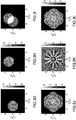
- FIG. 3A shows an electron microscope image of a sample, formed in this example of resin rods deposited on a glass substrate.
- FIGS. 3B to 3N show different steps of an exemplary method according to the present description, for computing from a plurality of interferograms, the phase and/or the modulus of an equivalent reflectivity of the sample.
- FIG. 3O shows the dark field image obtained using a method of the prior art.
- the set-up is the one shown in FIG. 2A .
- the light source 220 is a supercontinuum laser filtered at 475 nm with a spectral width of 6 nm thanks to a variable bandpass filter.
- the laser beam is linearly polarized and crosses a motorized half wave plate 221 to adjust the polarization direction.
- a fast steering mirror 222 permits to control the deflection of the beam, and a beam expander 223 generates a wide collimated beam.
- the center of the mirror is conjugated with the center of the sample through the beam expander, the tube lens 225 and the microscope objective 230. Thus, rotating the mirror varies the illumination angle without shifting laterally the beam on the object.
- the signal is imaged on a sCMOS camera after passing through relay lenses 241, 242 to obtain a global magnification of about 290.
- the half wave plate 221 is rotated so that the polarization of the illumination remains in TE configuration for each illumination angle.
- the sample comprises 12 calibrated resin rods forming a star and deposited on a glass slide.
- the inner diameter of the star is 800 nm, and each of its twelve branches has a width of 90 nm and a length of 400 nm. Height of the sample is 160 nm.
- the resin star was illuminated in TIR with six sequential illumination beams having a polar angle about 60°, and azimuth angles regularly spaced every 60°.
- FIG 3B and 3C show two interferograms acquired by the camera for two azimuth angles of the illumination beam.
- FIG. 3D shows the sum of all six interferograms for the six TIR illumination beams without any post-treatment.
- E Si E Ri * and E Si *E Ri in Eq. (1) are present and only the real part of r eq can be retrieved.
- this simple technique does not enable to correct from aberrations, thus providing a distorted map of the real part of the equivalent reflectivity r eq of the sample.
- FIG. 3E and 3F show the 2D Fourier transform of the interferograms shown in FIGS 3B and 3C respectively, with clear separation of E Si and E Si *.
- ⁇ 2 is too weak to be distinguished, and therefore the phase and modulus of E Si can be retrieved as in off-axis holography. Note that for the present sample the contrast between resin and air is far larger than for biological samples in water, therefore the condition
- FIGS. 3G and 3H show the modulus of the filtered fields Esi in the Fourier space for the two azimuth angles, after filtering of the signals shown respectively in FIGS. 3E and 3F .
- the synthetic aperture could in principle be generated simply by adding the fields shown in FIGS. 3G and 3H for each illumination.
- the reconstruction of r eq may simply comprise summing in the Fourier space the retrieved backscattered fields Esi for each illumination angle.
- the equivalent reflectivity r eq may then be reconstructed in phase and modulus from the 2D inverse Fourier transform of this sum.
- each field Esi may present a phase mismatch from one illumination to another. This originates from the fact that each field Esi is retrieved with a particular constant added on its phase, namely the phase of E Ri *. If the same polar angle is used from one illumination to another, this constant should remain the same, but in practice this may not be perfectly the case, and moreover the phase of E Ri * may be corrupted by the objective due to aberrations present at the edge of the numerical aperture. Before summing the different fields Esi, it is thus advantageous to normalize them between each other.
- Such a normalization procedure may correct the phase mismatch from one illumination beam to another, as well as the modulus mismatch which may arise from intensity fluctuations of the illumination beam from one illumination angle to another.
- FIGS. 3J and 3K show the building of the synthetic aperture (modulus and phase) by adding in Fourier space the filtered scattered field for the six illumination angles, with the normalization procedure.
- FIG. 3L shows the modulus of FIG. 3J after deletion of the central specular zone to get a dark field reconstruction.
- the equivalent reflectivity r eq can then be reconstructed in modulus and phase by doing the 2D inverse Fourier transform of the synthetic aperture.
- FIGS. 3M and 3N represent the squared modulus (intensity reflectivity) and the phase of r eq , with a clearly improved resolution compared to the approach of F.
- Garnger et al. obtained by adding the intensities of the scattered fields for each TIR illumination angle ( FIG. 3O ).
- the separation distance between the branches at the center of the star is about 130 nm, clearly below the Rayleigh criterion of about 200 nm imposed by the objective.
- Our reconstruction technique is presently run in less than five seconds on a standard laptop, but we believe this time can be shortened below one second with program optimization, so the method is compatible with in-vivo imaging.
- FIG. 4A shows a further embodiment of a device for TIR microscopy combining the method for TIR microscopy according to the present description and fluorescent measurement (TIRF).
- TIRF fluorescent measurement
- the device 400 A shown in FIG. 4A comprises, similarly to the device 200 of FIG. 2A , an illumination path of the sample with a spatially coherent light source 420, an (optional) wave plate 421, scanning means 422, a beam expander 423, a beam splitter 424, a tube lens 425 with a back focal plane 426 and a microscope objective 430 having a back focal plane (or exit pupil) 431, for example an immersion objective, working with a liquid immersion medium 432.
- the light source 420 is advantageously a laser source, thus having sufficient power and temporal coherence for fluorescence to be detected and filtered from scattering.
- the device 400 A further comprises a first detection path comprising said microscope objective 430, a bidimensional optical acquisition device 440 with a detection plane 445, and optional relay lenses 441, 442 defining a magnifier system with a plane 443 conjugated with the exit pupil 431 of the objective.
- the device 400 A further comprises a computing device 450 configured to receive input data 451 from said acquisition device and perform the numerical treatments for implementing the methods according to the present description.
- the device 400 A further comprises a second detection path, comprising said microscope objective 430 and a second bidimensional optical acquisition device 460 for acquisition of a fluorescence signal resulting from the fluorescence of the sample.
- An (optional) optical lens 462 enables an optical conjugation between the interface 211 and a detection plane 465 of said second bidimensional optical acquisition device 460.
- the computing device 450 is configured to receive input data 452 from said second acquisition device 460.
- a beam splitter 46 for example a dichroic beam splitter, is used to separate spectrally the reflected beam R 1 and backscattered signal beam S 1 on the one hand, and the fluorescence signal F 1 on the other hand, such that the reflected beam R 1 and backscattered signal beam S 1 are directed to the first bidimensional optical acquisition device 440 and the fluorescence signal F 1 is directed to the second bidimensional optical acquisition device 460.
- Such an arrangement enables to couple the high-resolution reconstruction of the scattering physical parameter of the sample to the characterization of the fluorescence contrast of the object in a single acquisition.
- the illumination path may be modified to perform structured illumination total internal reflection fluorescence microscopy (TIRF-SIM), which improves the resolution by a factor 2 compared to classical TIRF microscopy, as explained for example in M. G. L. Gustafsson, Journal of Microscopy, Vol. 198, p. 82, 2000 .
- TIRF-SIM structured illumination total internal reflection fluorescence microscopy
- TIRF-SIM may be performed using a beam shaper element 427 adapted to form simultaneously a first illumination beam I 1 and a second illumination beam I 2 , wherein the first and second illumination beams are symmetric with respect to the optical axis of the device (they have the same polar angle and two azimuth angles spaced by 180°).
- Such two coherent illumination beams structure the illumination as a light grid on the sample, with dark and bright interferences fringes.
- the beam shaper element 427 is for example a diffraction grating which creates diffraction orders +1 and -1. All other orders are blocked and the grating is coupled to a translation mount to shift the light grid successively to different positions so that the entire sample is illuminated with the bright fringes.
- an adapted spatial filter 444 for example a half-ring spatial filter, may be inserted in the first detection path, as described below.
- the scattered signal in bright field contains the total reflections E R1 e i ⁇ and E R2 e -i ⁇ which corresponds to each of the two illuminations, and the two corresponding scattered fields E S1 e i ⁇ and E S2 e -i ⁇ , where ⁇ is a controlled phase shift permitting to adjust the position of the light grid.
- an adapted spatial filter 444 in a plane conjugated with the exit pupil (or back focal plane 431) of the objective (for instance a half-ring placed at the edge of the pupil).
- adding to a TIRF-SIM apparatus a supplementary detection path to measure the backscattered signal opens the way to simultaneous super-resolved microscopy for both fluorescence and scattering.
- any TIRF microscopy setup can become a phase microscope by detecting the interference between the scattered field and the total internal reflection, as in off-axis holography but without the need of any external reference wave.
- it is possible to perform a synthetic aperture reconstruction of the sample which typically improves the resolution by a factor of 2 compared to classical microscopy techniques plagued by the Rayleigh criterion.
- retrieving both the intensity and the phase of the scattered field permits to study the probed samples with two different image contrasts, which is richer than using intensity only information as conventionally done in non-fluorescent TIR microscopy.
- the method for TIR microscopy according to the present description and the device for implementing said method comprise various variants, modifications and improvements which will be obvious to those skilled in the art, it being understood that these various variants, modifications and improvements form part of the scope of the invention as defined by the following claims.
Landscapes
- Physics & Mathematics (AREA)
- Health & Medical Sciences (AREA)
- Life Sciences & Earth Sciences (AREA)
- Chemical & Material Sciences (AREA)
- Analytical Chemistry (AREA)
- Biochemistry (AREA)
- General Health & Medical Sciences (AREA)
- General Physics & Mathematics (AREA)
- Immunology (AREA)
- Pathology (AREA)
- Microscoopes, Condenser (AREA)
Abstract
According to a first aspect, the present description relates to a device for TIR microscopy of a sample (S) comprising a support (210) for receiving the sample ; an illumination path comprising a spatially coherent light source (220) and a microscope objective (230), wherein said illumination path is configured to form at least a first illumination beam (I) for illuminating an interface (211) between said support and the sample, said first illumination beam having a first azimuth angle (φ) and a first polar angle (θ) adapted for total internal reflection at said interface, thus forming a first evanescent electromagnetic field (E) in the sample ; at least a first detection path comprising said microscope objective and a first bidimensional optical acquisition device (240), wherein said first detection path is configured for the acquisition of at least a first interferogram (N) resulting from the optical interference between at least a first reference electromagnetic field (E) and at least a first backscattered signal electromagnetic field (E), wherein said first reference electromagnetic field (E) results from the total internal reflection of said first illumination beam at said interface and said first backscattered signal electromagnetic field (E) results from the backscattering by the sample of said first evanescent electromagnetic field (E); and a computing device (250) configured to compute from said at least first interferogram at least one a map of a physical parameter related to the sample.
Description
- The present description relates to devices and methods for total internal reflection microscopy, and applies in particular to label-free optical imaging of samples.
- Total internal reflection fluorescence (TIRF) microscopy is a reference technique to study the membrane dynamics and organization in biological cells (See for example D. Axelrod et al., "Cell-substrate contacts illuminated by total internal reflection fluorescence", The Journal of cell biolology 89, 141 (1981)). Its main advantage is the ability to illuminate the sample over a thin slice of about 100 nm, by taking benefit from a total internal reflection (TIR) configuration.
- As shown in
FIG.1 , a sample S is deposited on acover slip 10, for example a glass substrate, and by illuminating through the substrate above the critical angle (illumination beam 11), anevanescent wave 12 is created at the interface to locally probe the sample. In the example shown inFIG. 1 , a high numericalaperture immersion objective 13 is used, to both illuminate above the critical angle and collect thefluorescence signal 14. Compared to standard wide field fluorescence microscopy, images with highly improved contrast are provided, since the background signal stemming from the volume of the sample can be suppressed. - Using fluorophores as contrast agents however presents some drawbacks, as their addition is invasive and induces the increased risk of photo bleaching and photo toxicity to the cell. Long-term studies are therefore difficult to achieve. In addition, the specificity of labeling prevents the visualization of the whole sample; it is therefore at the same time the main advantage and the main limitation of fluorescence imaging. As a result, there is a need for a high resolution technique able to probe cell membranes without the constraint of incorporating a fluorescent label.
- Two main approaches have been used so far to perform label-free imaging in total internal reflection (TIR) microscopy with a high numerical aperture objective.
- A first approach is described for example in P. Bon et al. ("Label-free evanescent microscopy for membrane nano-tomography in living cells", Journal of Biophotonics 7, 857 (2014)). This technique uses a spatially incoherent source (such as a light bulb or LED) to illuminate the sample simultaneously with all angles above the critical value imposed by the glass substrate and the sample immersion medium (usually water). As the sample refractive index is higher than that of water, total internal reflection is frustrated at locations where the sample is close to the interface, which modulates the reflected intensity. This modulation of the reflection is the source of contrast in the resulting image. This method is also known as "frustrated" total internal reflection or fTIR. Although this method presents a good sensitivity, the spatial resolution is limited to the Rayleigh criterion (0.6 λm/NA, where λm is the average wavelength of illumination and NA the numerical aperture of the objective), and the method amounts to considering the sample as a succession of planar diopters placed at different heights. This method is thus preferably adopted for samples having soft and progressive profiles of height.
- The second approach uses a laser beam focused in the back focal plane (BFP) of the objective at the edge of the numerical aperture (See for example F. Jünger et al., "Fast, label-free super-resolution live-cell imaging using rotating coherent scattering (ROCS) microscopy", ). The focused beam is scanned along a circle in the BFP, so that the sample is illuminated in TIR by a rotating collimated beam, and the integration time of the camera is set to match the rotation period of the beam. The totally reflected beam is blocked in a plane conjugated with the BFP to detect only the scattered intensity and obtain dark field imaging. Although this method claims a good spatial resolution (slightly better than the Rayleigh criterion), it is principally used for qualitative measurements as it is known to slightly distort the image compared to the object.
- The present invention proposes a new method for total internal reflection microscopy, which can provide with a simple arrangement the phase of the signal backscattered by the sample and further improves the imaging spatial resolution compared to the previous approaches.
- According to a first aspect, the present description relates to a device for TIR microscopy of a sample comprising:
- a support for receiving the sample;
- an illumination path of the sample comprising a spatially coherent light source and a microscope objective, wherein said illumination path is configured to form at least a first illumination beam for illuminating an interface between said support and the sample, said first illumination beam having a first azimuth angle and a first polar angle adapted for total internal reflection at said interface, thus forming a first evanescent electromagnetic field in the sample;
- at least a first detection path comprising said microscope objective and a first bidimensional optical acquisition device, wherein said first detection path is configured for the acquisition of at least a first interferogram resulting from the optical interference between at least a first reference electromagnetic field and at least a first backscattered signal electromagnetic field, wherein said first reference electromagnetic field results from the total internal reflection of said first illumination beam at said interface and said first backscattered signal electromagnetic field results from the backscattering by the sample of said first evanescent electromagnetic field; and
- a computing device configured to compute from said at least first interferogram at least one map of a physical parameter related to the sample.
- The device for TIR microscopy as described above enables a label-free TIR microscopy technique, which keeps the same set-up simplicity as the previous approaches for TIR microscopy but also permits to perform phase imaging. By detecting the interference between the backscattered field and the total internal reflection, an off-axis holography scheme is provided but without the need of any external reference wave.
- According to one or further embodiments, said at least one map (or "image") of a physical parameter related to the sample comprises at least one of: a 2D map of the phase and/or modulus of said first backscattered signal electromagnetic field, a 2D map of the real part and/or imaginary part and/or modulus and/or phase of an equivalent reflectivity req of the sample, a 3D map of the real and/or imaginary parts of a permittivity contrast Δε of the sample. The permittivity contrast Δε may be defined as the difference between the relative dielectric permittivity of the object (the square of the refractive index) and that of the background.
- According to one or further embodiments, said illumination path further comprises scanning means for controlling said azimuth angle and/or said polar angle of at least said first illumination beam. For example, the scanning means comprise at least a first axis of rotation situated in a plane optically conjugated with said interface between the sample and the support.
- According to one or further embodiments, the scanning means are configured to form a temporal sequence of illumination beams, including said first illumination beam, and having different azimuth and/or polar angles adapted for total internal reflection at said interface, each illumination beam thus forming an evanescent electromagnetic field in the sample; the first detection path is configured for the acquisition of a plurality of interferograms, each interferogram resulting from the optical interference between at least one reference electromagnetic field and at least one backscattered signal electromagnetic field, wherein said reference electromagnetic field results from the total internal reflection of one of said illumination beams at said interface and said backscattered signal electromagnetic field results from the scattering by the sample of said evanescent electromagnetic field formed by said illumination beam; the computing device is configured to compute said at least one map of a physical parameter related to the sample from said plurality of interferograms.
- By using several illumination angles, for example having the same polar angle but different azimuth angles, it is possible to perform a synthetic aperture reconstruction of the sample, the improving the resolution by a factor of 2 compared to classical microscopy techniques plagued by the Rayleigh criterion.
- In the present description, the resolution is defined by the smallest distance between two points of the object that can be distinguished through the microscope objective.
- According to one or further embodiments, the device for TIR microscopy further comprises a second detection path, wherein said second detection path comprises said microscope objective, a second bidimensional optical acquisition device for acquisition of a fluorescence signal resulting from the fluorescence of said sample and a beam splitter configured to direct said fluorescence signal to said second bidimensional optical acquisition device.
- According to one or further embodiments, said illumination path further comprises a beam shaper element adapted to form simultaneously said first illumination beam and a second illumination beam, wherein the first and second illumination beams have the same polar angle and two azimuth angles spaced by 180°.
- According to one or further embodiments, said first acquisition path further comprises a spatial filter for blocking one of the first and second reflections beams, resulting respectively from the total internal reflection of said first and second illumination beams at said interface between the sample and the support.
- According to a second aspect, the present description relates to a method for TIR microscopy of a sample comprising the steps of:
- illuminating with at least a first illumination beam an interface between a support and the sample using an illumination path comprising a spatially coherent light source and a microscope objective, wherein said first illumination beam has a first polar angle adapted for total internal reflection at said interface and a first azimuth angle, thus forming a first evanescent electromagnetic field in the sample;
- detecting, using a first detection path comprising said microscope objective and a first bidimensional optical acquisition device, at least a first interferogram resulting from the optical interference between at least a first reference electromagnetic field and at least a first backscattered signal electromagnetic field, wherein said first reference electromagnetic field results from the total internal reflection of said first illumination beam at said interface and said first backscattered signal electromagnetic field results from the scattering by the sample of said first evanescent electromagnetic field; and
- computing, from at least said first interferogram, at least one a map of a physical parameter related to the sample.
- According to one or further embodiments, the computing step comprises performing a numerical 2D Fourier transform of said at least first interferogram and filtering said 2D Fourier transform to retrieve the 2D Fourier transform of said first backscattered signal electromagnetic field. It is thus possible to retrieve a 2D map of the phase and/or modulus of said first backscattered signal electromagnetic field.
- According to one or further embodiments, the illuminating step comprises sequentially illuminating said interface with a plurality of illumination beams, including said first illumination beam and having different azimuth angles and polar angles adapted for total internal reflection at said interface, each illumination beam thus forming an evanescent electromagnetic field in the sample; the detecting step comprises acquiring a plurality of interferograms, each interferogram resulting from the optical interference between at least one reference electromagnetic field and at least one backscattered signal electromagnetic field, wherein said reference electromagnetic field results from the total internal reflection of one of said illumination beams at said interface and said backscattered signal electromagnetic field results from the scattering by the sample of an evanescent electromagnetic field formed by said illumination beam in the sample; the computing step comprises computing, from said plurality of interferograms, at least one map of a physical parameter related to the sample.
- It is thus possible to perform a synthetic aperture reconstruction of the sample, which typically improves the resolution by a factor of 2 compared to classical microscopy techniques plagued by the Rayleigh criterion.
- Said at least one map of a physical parameter related to the sample may comprise at least one of: a 2D map of the phase and/or modulus of a backscattered signal electromagnetic field resulting from the scattering by the sample of the evanescent electromagnetic field formed by any of the illumination beams, a 2D map of an equivalent reflectivity req of the sample, a 3D map of permittivity contrast Δε of the sample. A 2D map of an equivalent reflectivity req of the sample, or a 3D map of permittivity contrast Δε of the sample may be retrieved from one or a plurality of said 2D maps of backscattered signal electromagnetic fields, or directly from one or a plurality of said interferograms.
- According to one or further embodiments, the computing step comprises performing a summation of said plurality of interferograms. It is thus possible to directly retrieve a 2D map of the real part of an equivalent reflectivity req of the sample.
- According to one or further embodiments, the computing step comprises:
- performing a numerical 2D Fourier transform of each interferogram;
- filtering said 2D Fourier transform to retrieve the 2D Fourier transform of the backscattered signal electromagnetic field for each illumination angle;
- summing said 2D Fourier transforms of the backscattered signal electromagnetic fields for all illumination angles;
- performing an inverse 2D Fourier transform of said sum to obtain a 2D map of the phase and/or modulus of an equivalent reflectivity of the sample.
- According to one or further embodiments, the computing step further comprises normalizing the 2D Fourier transform of the backscattered signal electromagnetic field for each illumination angle before summing, to correct from a phase and/or modulus mismatch between the different backscattered signal electromagnetic fields in the Fourier domain.
- According to one or further embodiments, the method for TIR microscopy further comprises acquiring using a second detection path, a fluorescence signal resulting from the fluorescence of the sample.
- It is thus possible to get simultaneously TIR fluorescence microscopy and TIR microscopy according to the present description.
- According to one or further embodiments, the illuminating step comprises simultaneously illuminating said interface with said first illumination beam and a second illumination beam, wherein the first and second illumination beams have the same polar angle and two azimuth angles spaced by 180°.
- According to one or further embodiments, the detecting step further comprises blocking one of the first and second reflections beams, resulting respectively from the total internal reflection of said first and second illumination beams at said interface between the sample and the support.
- Other advantages and features of the object of the description will become apparent upon reading of the description, illustrated by the following figures:
-
FIG. 1 (already described), a scheme for TIRF microscopy, according to the prior art; -
FIG. 2A , a scheme of a device for total internal reflection (TIR) microscopy, according to an embodiment of the present description;FIG. 2B , a scheme of an illumination beam impinging the interface between the sample and the substrate; andFIG. 2C , a detailed view of said interface, illustrating the different optical fields; -
FIG. 3A to 3O , experimental images illustrating an electron microscope image of a sample (FIG. 3A ); different steps of a method for total internal reflection microscopy according to an embodiment of the present description for determining the modulus and phase (real part/ complex part) of an equivalent reflectivity of such sample (FIGS. 3B to 3N ); and for comparison, the dark field image obtained using a method of the prior art (FIG. 3O ); -
FIG. 4A , a scheme of a device for total internal reflection microscopy, according to an embodiment of the present description, combined with TIR fluorescence microscopy andFIG. 4B , the same scheme of a device for TIR microscopy as the one shown inFIG. 4A , further implementing a structured illumination. - Specific embodiments of the present disclosure will now be described in detail with reference to the accompanying figures. In the following detailed description of embodiments of the present disclosure, numerous specific details are set forth in order to provide a more thorough understanding of embodiments of the present disclosure. However, it will be apparent to one of ordinary skill in the art that embodiments of the present disclosure may be practiced without these specific details. In other instances, well-known features have not been described in detail to avoid unnecessarily complicating the description.
- Herein, the words "comprise/comprising" mean the same thing as "include/including," "contain/containing", are inclusive or open-ended and do not exclude additional, unrecited elements. Limit values of ranges using for example the words "from", "from...to", "below", "more than", "greater than", "less than", "lower than", and "at least" and the like are considered included in the ranges.
-
FIG. 2A is a schematic view of an exemplary architecture of adevice 200 for TIR microscopy of a sample in an EPI configuration for detecting the total internal reflection. Thedevice 200 includes asupport 210 for receiving the sample. A detailed view of aninterface 211 between the support and the sample is shown inFIG. 2C . - The support is for example made of glass, or any transparent medium which permits to generate total internal reflection at
interface 211. - The sample may be any object in a surrounding medium (e.g. liquids or air), i.e.any micro or nanostructure having a refractive index is different from that of the medium. For example, the sample may be a biological sample in solution, or a micro or nanostructure directly deposited on the support, e.g. biochips. In general, a low refractive index difference between the object and the medium, e.g. Δn < 0.5, will provide a better performance of the measurements, as the field backscattered by the object will be weak compared to the total internal reflection.
- The
device 200 for TIR microscopy further includes an illumination path of the sample comprising a spatially coherentlight source 220 and amicroscope objective 230 with a back focal plane (BFP) 231, also referred to as the Fourier plane. The illumination path is configured to form at least a first illumination beam I1 for illuminating theinterface 211 between thesupport 210 and the sample S. - The spatial
coherent source 220 is for example a laser source, a laser diode or any light source where light is sufficiently spatially filtered (through a pinhole, a monomode fiber...) so that each illumination angle throughmicroscope objective 230 is defined with a typical angle variation in radians of λm/(10D), where λm is the average wavelength of the illumination beam and D is the maximal diameter of the sample. - In some embodiments, the beam I0 emitted by the
source 220 may be a linearly polarized laser beam, in which case the illumination path may further comprise awave plate 221, for example a motorized wave plate, adapted to adjust the polarization direction of the laser beam I0. - In the exemplary architecture of the
device 200 shown inFIG. 2A , the illumination path further comprises scanning means 222 to control the polar angle and azimuth angle of the illumination beam and abeam expander 223 for generating a wide collimated beam. The illumination path further comprises abeam splitter 224 to direct the collimated beam towards themicroscope objective 230 and atube lens 225, whose front focal plane is superposed with the backfocal plane 231 of the objective. - As shown in
FIG. 2B , at least a first collimated illumination beam I1 is thus generated at the exit of themicroscope objective 230, wherein said illumination beam I1 is impinging on the interface between the sample and the support (plane xOy inFIG. 2B ) with a first azimuth angle φ1 and a first polar angle (or tilt angle) θ1. The polar angle θ1 is adapted for total internal reflection of the first illumination beam I1 at theinterface 211 between the support and the sample. - Scanning means 222 may comprise a rotary optic, for example a combination of galvanometric systems or a combination of MEMS mirrors (with one axis) or one MEMS mirror with two axes. In the case where two distinct mirrors are used to produce these two rotations, it is advantageous for the axes of rotation of these two mirrors to be optically conjugated. Advantageously, the axis (axes) of rotation of the angular scanning is (are) situated in optically conjugate plane(s) of said interface between the sample and the support. Thus, rotating the mirror(s) varies the illumination angle(s) without shifting laterally the illumination beam on the object.
- The
microscope objective 230 is for example an immersion objective, working with aliquid immersion medium 232 placed between thesupport 210 and the objective. The liquid immersion medium has the same refractive index as the one of thesupport 210 to obtain a single reflection atinterface 211. For example, the liquid immersion medium is oil when thesupport 210 is a glass substrate. - As shown in
FIG. 2C , the first illumination beam I1, having an electromagnetic field EI1, has a polar angle θ1 adapted for total internal reflection at theinterface 211, thus forming a first evanescent electromagnetic field EE1 in the sample. The total internal reflection of the first illumination beam at theinterface 211 results in a first reflected beam R1 having a first reference electromagnetic field ER1. Further, an electromagnetic field ES1, hereafter the first backscattered signal electromagnetic field, is generated; it results from the backscattering of the first evanescent electromagnetic field EE1 by the sample S. - In the present description, the complex notation is assumed for all electromagnetic fields.
- The exemplary architecture of the
device 200 shown inFIG. 2A further includes a detection path comprising saidmicroscope objective 230, a bidimensionaloptical acquisition device 240, and acomputing device 250. - The bidimensional
optical acquisition device 240 is for example a CCD, CMOS or sCMOS camera. - The detection path is configured for the acquisition by the
acquisition device 240 of at least a first interferogram N1 resulting from the optical interference between the first reference electromagnetic field ER1 and the first backscattered signal electromagnetic field ES1. As shown inFIG. 2A , the detection path further comprises thetube lens 225, having a front focal plane superposed with the backfocal plane 231 of the objective and a backfocal plane 226. Theinterface 211 is optically conjugated with the backfocal plane 226 of thetube lens 225 when saidinterface 211 is placed on the front focal plane of the objective 230. Adetection plane 245 of theoptical acquisition device 240 is optically conjugated with saidinterface 211. Said detection plane can be placed for instance at said backfocal plane 226 of thetube lens 225. Optionally,relay lenses interface 211 and theacquisition device 240, or if it is useful to have access to an intermediate plane conjugated with the backfocal plane 231 of the objective (where spatial filters can be placed for instance). Such intermediate plane can be the backfocal plane 243 oflens 241, if its front focal plane is superposed with the backfocal plane 226 oftube lens 225. - The
computing device 250 for determining at least one map of a physical parameter related to the sample may be a computer, computer network, or other device that has a processor, memory, data storage, and other associated hardware such as an interface module, a display screen and a media drive for reading and writing a removable storage medium (not shown inFIG. 2A ). The removable storage medium and/or data storage may contain instructions, which when executed by thecomputing device 250, cause thecomputing device 250 to perform one or more example methods described herein. - In the example system of
FIG. 2A , thecomputing device 250 receivesincoming data 251, such as one or a plurality of electronic signals resulting from the acquisition by theacquisition device 240 of said at least first interferogram. Processing ofincoming data 251 by thecomputing device 250 may be made according to one or more example methods described herein. - In a first embodiment, a single interferogram may be used for retrieving the backscattered signal electromagnetic field ES1.
- Said first interferogram N1 corresponds to the intensity of the optical signal detected by the
acquisition device 240 and can be written:
- Where ER1* represents the complexe conjugate of ER1 and ES1* represents the complexe conjugate of ES1.
- Since the sample S is illuminated by an evanescent wave over a very thin slice, typically a layer having a thickness of about 100 nm or less, and is usually of very weak contrast in biology, we can assume ER1 is very strong compared to ES1, and neglect |ES1|^2 in Eq. (1). Since the reflective beam is close to the edge of the numerical aperture of the objective, it can then act as an off-axis reference wave for the backscattered signal, as in classical digital off-axis holography.
- By performing the 2D numerical Fourier transform of N1, the terms ES1ER1* and ES1*ER1 can be separated from each other in the Fourier space, and it is then possible to filter ES1 both in modulus and phase, from a simple measurement of an interferogram N1.
- Hence, the present invention is clearly different from the approach of P. Bon et al. described in the prior art section, which necessitates that total internal reflection does not take place in the presence of the sample. In the present invention, total internal reflection occurs in the presence of the sample to get the best performances, what supposes not to use the small illumination angles necessary in P. Bon et al.
- With the device and method for TIR microscopy according to the present description, a simple measurement of an interferogram N1 permits to obtain a 2D map of the phase and the modulus of the field ES1 at the level of the sample; such a configuration is far more simple than classical techniques to measure the phase and the modulus of an optical backscattered signal, which necessitate for instance to add an external reference path or to use a wavefront sensor.
- As in known techniques of off-axis holography, additional numerical treatments can be made, for example numerical treatments of the field in the Fourier space, as for instance propagating the field to adjust its focus plane, or convert the field to dark field or phase contrast modes.
- According to one or a plurality of embodiments, several successive illuminations of the interface between the support and the sample are made, at different angles, thus generating a plurality of interferograms. For example, the azimuth angle is changed while keeping the same polar angle.
- For example, the scanning means 222 shown in
FIG. 2A are configured to form a plurality of p successive illumination beams Ii, for example p comprised between 4 and several hundreds For example, the p illumination beams Ii have the same polar angle but different azimuth angles. - Each illumination beam I; forms an evanescent electromagnetic field EEi in the sample. The detection path is then configured for the acquisition of p interferograms Ni, wherein each interferogram Ni results from the optical interference between at least one reference electromagnetic field ERi and at least one backscattered signal electromagnetic field ESi, wherein the reference electromagnetic field ERi results from the total internal reflection of said illumination beam Ii at said interface and said backscattered signal electromagnetic field ESi results from the scattering by the sample of said evanescent electromagnetic field EEi.
- From the set of p interferograms, different reconstruction techniques can be used to reconstruct a map of a physical parameter related to the sample, as for example a 2D map of the phase and/or modulus of the backscattered signal electromagnetic field for any of the illuminations, a 2D or 3D map of the permittivity contrast Δε or a 2D map of an equivalent reflectivity req, as it will be described in further details below.
- According to one or a plurality of examples, the reconstruction techniques comprise extracting p backscattered fields ESi from the p interferograms Ni, for example using a method as described above. Different other physical parameters (e.g. permittivity contrast Δε or equivalent reflectivity req) may then be retrieved from said p backscattered fields ESi.
- According to a first example, a 3D map of the permittivity contrast Δε may be retrieved with an inversion algorithm based on a 3D scattering model, as described for example in C. Godavarthi et al., JOSA A, Vol. 32, p. 287, 2015. Such an approach provides a very good resolution (better than λ/4), but at the cost of longer reconstruction procedures.
- According to a further example, a 3D map of the permittivity contrast Δε may be retrieved using 3D models based on linear approximations, such as Born or Rytov approximations. For each illumination angle, Esi permits to access different spatial frequencies of Δε, and combining information gathered with all angles permits to enlarge the accessible spatial frequency domain and obtain a super-resolved reconstruction of Δε (beyond the classical Rayleigh criterion). This is referred to as synthetic aperture microscopy, and described for example in Y. Cotte et al., Nature Photonics, Vol. 7, p. 113, 2013. In the case of the Born approximation, the field ESi(k Si, k Ii) scattered along wave vector k Si when the sample is illuminated by a plane wave of wave vector k Ii is linked to Δε by:

- According to a further example, a 2D model may be used to reconstruct an equivalent reflectivity req of the sample. Such equivalent reflectivity req may be derived from the signal backscattered fields ESi. As for example in S. A. Alexandrov et al., Phys. Rev. Lett., Vol. 97, 168102, 2006, it can be defined as ESi = reqEIi, and can be seen as an equivalent amplitude reflection coefficient of the sample.
- Such reconstruction technique is a 2D synthetic aperture technique, where the scattered field ESi(k Si, k Ii) is linked to req by :

interface 211. - An example of such 2D reconstruction is detailed and illustrated in the section below, with reference to
FIGS. 3A to 3O . - According to one or a plurality of examples, the reconstruction techniques comprise retrieving physical parameters (e.g. permittivity contrast Δε or equivalent reflectivity req) directly from the p interferograms Ni.
- For example, the permittivity contrast Δε may be retrieved from the p interferograms Ni with an inversion algorithm based on a rigorous 3D scattering model, but this time, as in M. D'Urso et al., JOSA A, Vol. 25, p. 271, 2008. Compared to the case as described above where input data are the p scattered fields ESi, this approach generally leads to still longer reconstruction processes with less accurate resolutions.
- According to another example, the p interferograms Ni may be directly summed, which will enable a reconstruction of the real part of the equivalent reflectivity req mentioned above. However in practice, as will be detailed in the next section, such simple reconstruction scheme may be corrupted by the aberrations of the objective. It can be considered to correct the impact of these aberrations on the signal by placing on the detection path a phase mask, created for example by a spatial light modulator (SLM), in a plane conjugated with the back focal plane of the objective (plane 231). If the aberrations of the objective have been measured in a preliminary step, it is then possible to generate a phase mask on the SLM which cancels aberrations before the signal reaches the camera.
- In the section below, it is shown experimentally how the phase and/or the modulus of an equivalent reflectivity of the sample may be retrieved using the original architecture of the device according to the present description.
-
FIG. 3A shows an electron microscope image of a sample, formed in this example of resin rods deposited on a glass substrate.FIGS. 3B to 3N show different steps of an exemplary method according to the present description, for computing from a plurality of interferograms, the phase and/or the modulus of an equivalent reflectivity of the sample.FIG. 3O shows the dark field image obtained using a method of the prior art. - The set-up is the one shown in
FIG. 2A . Thelight source 220 is a supercontinuum laser filtered at 475 nm with a spectral width of 6 nm thanks to a variable bandpass filter. The laser beam is linearly polarized and crosses a motorizedhalf wave plate 221 to adjust the polarization direction. Afast steering mirror 222 permits to control the deflection of the beam, and abeam expander 223 generates a wide collimated beam. The center of the mirror is conjugated with the center of the sample through the beam expander, thetube lens 225 and themicroscope objective 230. Thus, rotating the mirror varies the illumination angle without shifting laterally the beam on the object. TIR illumination of the sample and collection of the reflected intensity is performed through the microscope objective 230 (100x, NA = 1.49). The signal is imaged on a sCMOS camera after passing throughrelay lenses half wave plate 221 is rotated so that the polarization of the illumination remains in TE configuration for each illumination angle. - As shown in
FIG. 3A , the sample comprises 12 calibrated resin rods forming a star and deposited on a glass slide. The inner diameter of the star is 800 nm, and each of its twelve branches has a width of 90 nm and a length of 400 nm. Height of the sample is 160 nm. - The resin star was illuminated in TIR with six sequential illumination beams having a polar angle about 60°, and azimuth angles regularly spaced every 60°.
-
FIG 3B and 3C show two interferograms acquired by the camera for two azimuth angles of the illumination beam. -
FIG. 3D shows the sum of all six interferograms for the six TIR illumination beams without any post-treatment. Both terms ESiERi* and ESi*ERi in Eq. (1) are present and only the real part of req can be retrieved. However, this simple technique does not enable to correct from aberrations, thus providing a distorted map of the real part of the equivalent reflectivity req of the sample. -
FIG. 3E and 3F show the 2D Fourier transform of the interferograms shown inFIGS 3B and 3C respectively, with clear separation of ESi and ESi*. As expected, |ESi|^2 is too weak to be distinguished, and therefore the phase and modulus of ESi can be retrieved as in off-axis holography. Note that for the present sample the contrast between resin and air is far larger than for biological samples in water, therefore the condition |ESi| << |ERi| will be still more valid in this case. -
FIGS. 3G and 3H show the modulus of the filtered fields Esi in the Fourier space for the two azimuth angles, after filtering of the signals shown respectively inFIGS. 3E and 3F . - The synthetic aperture could in principle be generated simply by adding the fields shown in
FIGS. 3G and 3H for each illumination. - In other words, according to an embodiment, the reconstruction of req may simply comprise summing in the Fourier space the retrieved backscattered fields Esi for each illumination angle. The equivalent reflectivity req may then be reconstructed in phase and modulus from the 2D inverse Fourier transform of this sum.
- However in practice, the different fields Esi may present a phase mismatch from one illumination to another. This originates from the fact that each field Esi is retrieved with a particular constant added on its phase, namely the phase of ERi*. If the same polar angle is used from one illumination to another, this constant should remain the same, but in practice this may not be perfectly the case, and moreover the phase of ERi* may be corrupted by the objective due to aberrations present at the edge of the numerical aperture. Before summing the different fields Esi, it is thus advantageous to normalize them between each other.
- This issue can be solved by taking benefit from the spatial frequency overlap between the illuminations. According to Eq. (3) above, two neighbour illumination angles give access to common spatial frequencies of req, for which the scattered field should be the same in both cases. Thus each illumination is normalized with respect to its neighbour by multiplying its field by a complex factor which minimizes the discrepancy of the data in their common spatial frequency domain (as shown in
FIG. 3I for the two fields ofFIGS. 3G and 3H ). This can be done for instance with standard minimization functions implemented in Matlab®. - Such a normalization procedure may correct the phase mismatch from one illumination beam to another, as well as the modulus mismatch which may arise from intensity fluctuations of the illumination beam from one illumination angle to another.
-
FIGS. 3J and 3K show the building of the synthetic aperture (modulus and phase) by adding in Fourier space the filtered scattered field for the six illumination angles, with the normalization procedure. - Additional optional treatments in Fourier space can be performed. For example,
FIG. 3L shows the modulus ofFIG. 3J after deletion of the central specular zone to get a dark field reconstruction. The equivalent reflectivity req can then be reconstructed in modulus and phase by doing the 2D inverse Fourier transform of the synthetic aperture. -
FIGS. 3M and 3N represent the squared modulus (intensity reflectivity) and the phase of req, with a clearly improved resolution compared to the approach of F. Jünger et al., obtained by adding the intensities of the scattered fields for each TIR illumination angle (FIG. 3O ). - The separation distance between the branches at the center of the star is about 130 nm, clearly below the Rayleigh criterion of about 200 nm imposed by the objective. Our reconstruction technique is presently run in less than five seconds on a standard laptop, but we believe this time can be shortened below one second with program optimization, so the method is compatible with in-vivo imaging.
-
FIG. 4A shows a further embodiment of a device for TIR microscopy combining the method for TIR microscopy according to the present description and fluorescent measurement (TIRF). - The
device 400A shown inFIG. 4A comprises, similarly to thedevice 200 ofFIG. 2A , an illumination path of the sample with a spatially coherentlight source 420, an (optional)wave plate 421, scanning means 422, abeam expander 423, abeam splitter 424, atube lens 425 with a backfocal plane 426 and amicroscope objective 430 having a back focal plane (or exit pupil) 431, for example an immersion objective, working with aliquid immersion medium 432. Thelight source 420 is advantageously a laser source, thus having sufficient power and temporal coherence for fluorescence to be detected and filtered from scattering. Thedevice 400A further comprises a first detection path comprising saidmicroscope objective 430, a bidimensionaloptical acquisition device 440 with adetection plane 445, andoptional relay lenses plane 443 conjugated with theexit pupil 431 of the objective. Thedevice 400A further comprises acomputing device 450 configured to receiveinput data 451 from said acquisition device and perform the numerical treatments for implementing the methods according to the present description. - In the example of
FIG. 4A , thedevice 400A further comprises a second detection path, comprising saidmicroscope objective 430 and a second bidimensionaloptical acquisition device 460 for acquisition of a fluorescence signal resulting from the fluorescence of the sample. An (optional)optical lens 462 enables an optical conjugation between theinterface 211 and adetection plane 465 of said second bidimensionaloptical acquisition device 460. Thecomputing device 450 is configured to receiveinput data 452 from saidsecond acquisition device 460. - A
beam splitter 461, for example a dichroic beam splitter, is used to separate spectrally the reflected beam R1 and backscattered signal beam S1 on the one hand, and the fluorescence signal F1 on the other hand, such that the reflected beam R1 and backscattered signal beam S1 are directed to the first bidimensionaloptical acquisition device 440 and the fluorescence signal F1 is directed to the second bidimensionaloptical acquisition device 460. - Such an arrangement enables to couple the high-resolution reconstruction of the scattering physical parameter of the sample to the characterization of the fluorescence contrast of the object in a single acquisition.
- Such characterization of the fluorescence contrast is known and described for example in M. Brunstein et al., Biophysical Journal, Vol. 106, p. 1020, 2014.
- According to some further embodiments as shown for example in the
device 400B ofFIG. 4B , the illumination path may be modified to perform structured illumination total internal reflection fluorescence microscopy (TIRF-SIM), which improves the resolution by afactor 2 compared to classical TIRF microscopy, as explained for example in M. G. L. Gustafsson, Journal of Microscopy, Vol. 198, p. 82, 2000. As shown inFIG. 4B , TIRF-SIM may be performed using abeam shaper element 427 adapted to form simultaneously a first illumination beam I1 and a second illumination beam I2, wherein the first and second illumination beams are symmetric with respect to the optical axis of the device (they have the same polar angle and two azimuth angles spaced by 180°). Such two coherent illumination beams structure the illumination as a light grid on the sample, with dark and bright interferences fringes. - The
beam shaper element 427 is for example a diffraction grating which creates diffraction orders +1 and -1. All other orders are blocked and the grating is coupled to a translation mount to shift the light grid successively to different positions so that the entire sample is illuminated with the bright fringes. - With structured illumination, the reconstruction techniques of TIR microscopy according to the present description can still be implemented. In particular, reconstruction techniques directly using the interferograms as described above can be carried out with structured illumination. For extracting the backscattered fields from the interferograms, an adapted
spatial filter 444, for example a half-ring spatial filter, may be inserted in the first detection path, as described below. - In the presence of the light grid, the scattered signal in bright field contains the total reflections ER1eiϕ and ER2e-iϕ which corresponds to each of the two illuminations, and the two corresponding scattered fields ES1eiϕ and ES2e-iϕ, where ϕ is a controlled phase shift permitting to adjust the position of the light grid.
- To perform self-referenced phase microscopy in these conditions, it is possible to block one of the two total reflections by placing an adapted
spatial filter 444 in a plane conjugated with the exit pupil (or back focal plane 431) of the objective (for instance a half-ring placed at the edge of the pupil). - The detected intensity N then becomes:


- Since once again scattered fields are weak compared to the total internal reflection, for a given position of the light grid, it is possible to filter in the 2D Fourier space the sum (ES1 + ES2e-i2ϕ). By using at least a second position of the grid, fields ES1 and ES2 can be simply obtained by solving a two unknown equation system. Once these fields have been extracted, the same reconstruction techniques as those explained previously can be applied.
- Usually in TIRF-SIM microscopy, three orientations of the light grid are used every 60°, and for each of them the grid is shifted at three positions every third of period, which give 9 measurements in total. The use of a fixed half-ring filter as the
spatial filter element 444 is thus a simple solution to block one of the two total reflections for each of the three orientations of the grid. - In the end, adding to a TIRF-SIM apparatus a supplementary detection path to measure the backscattered signal opens the way to simultaneous super-resolved microscopy for both fluorescence and scattering.
- More generally, we have shown above that any TIRF microscopy setup can become a phase microscope by detecting the interference between the scattered field and the total internal reflection, as in off-axis holography but without the need of any external reference wave. By using several azimuth illumination angles, it is possible to perform a synthetic aperture reconstruction of the sample, which typically improves the resolution by a factor of 2 compared to classical microscopy techniques plagued by the Rayleigh criterion. Moreover, retrieving both the intensity and the phase of the scattered field permits to study the probed samples with two different image contrasts, which is richer than using intensity only information as conventionally done in non-fluorescent TIR microscopy. With an appropriate model, we believe this can lead to improved estimations of quantitative parameters like axial dimensions and refractive index of the sample, as in tomographic diffractive microscopy (see for example C. Godavarthi et al., JOSA A, Vol. 32, p. 287, 2015).
- Although described in a number of exemplary embodiments, the method for TIR microscopy according to the present description and the device for implementing said method comprise various variants, modifications and improvements which will be obvious to those skilled in the art, it being understood that these various variants, modifications and improvements form part of the scope of the invention as defined by the following claims.
Claims (15)
- A device for TIR microscopy of a sample (S) comprising:- a support (210) for receiving the sample;- an illumination path of the sample comprising a spatially coherent light source (220) and a microscope objective (230), wherein said illumination path is configured to form at least a first illumination beam (I1) for illuminating an interface (211) between said support and the sample, said first illumination beam having a first azimuth angle (φ1) and a first polar angle (θ1) adapted for total internal reflection at said interface, thus forming a first evanescent electromagnetic field (EE1) in the sample ;- at least a first detection path comprising said microscope objective and a first bidimensional optical acquisition device (240), wherein said first detection path is configured for the acquisition of at least a first interferogram (N1) resulting from the optical interference between at least a first reference electromagnetic field (ER1) and at least a first backscattered signal electromagnetic field (ES1), wherein said first reference electromagnetic field (ER1) results from the total internal reflection of said first illumination beam at said interface and said first backscattered signal electromagnetic field (ES1) results from the backscattering by the sample of said first evanescent electromagnetic field (EE1); and- a computing device (250) configured to compute from said at least first interferogram at least one map of a physical parameter related to the sample.
- The device for TIR microscopy according to claim 1, wherein said illumination path further comprises scanning means (222) for controlling said azimuth angle and/or said polar angle of at least said first illumination beam.
- The device for TIR microscopy according to claim 2, wherein:- said scanning means are configured to form a temporal sequence of illumination beams (Ii) including said first illumination beam, wherein said illumination beams (Ii) have different azimuth and/or polar angles adapted for total internal reflection at said interface, each illumination beam (I;) thus forming an evanescent electromagnetic field (EEi) in the sample;- said first detection path is configured for the acquisition of a plurality of interferograms, each interferogram (Ni) resulting from the optical interference between at least one reference electromagnetic field (ERi) and at least one backscattered signal electromagnetic field (ESi), wherein said reference electromagnetic field results from the total internal reflection of one of said illumination beams at said interface and said backscattered signal electromagnetic field results from the scattering by the sample of an evanescent electromagnetic field formed by said illumination beam;- said computing device is configured to compute said at least one map of a physical parameter related to the sample from said plurality of interferograms.
- The device for TIR microscopy according to any of the preceding claims, wherein said at least one map of a physical parameter related to the sample comprises at least one of: a 2D map of the phase and/or modulus of said first backscattered signal electromagnetic field, a 2D map of an equivalent reflectivity req of the sample, a 3D map of a permittivity contrast Δε of the sample.
- The device for TIR microscopy according to any of the preceding claims, further comprising a second detection path, wherein said second detection path comprises said microscope objective, a second bidimensional optical acquisition device (460) for acquisition of a fluorescence signal resulting from the fluorescence of said sample and a beam splitter (461) configured to direct said fluorescence signal to said second bidimensional optical acquisition device.
- The device for TIR microscopy according to claim 5, wherein:- said illumination path further comprises a beam shaper element (427) adapted to form simultaneously said first illumination beam (I1) and a second illumination beam (I2), wherein the first and second illumination beams have the same polar angle and two azimuth angles spaced by 180°.
- The device for TIR microscopy according to claim 6, wherein:- said first acquisition path further comprises a spatial filter (444) for blocking one of the first and second reflections beams (R1, R2), resulting respectively from the total internal reflection of said first and second illumination beams at said interface (211) between the sample and the support.
- A method for TIR microscopy of a sample (S) comprising the steps of:- illuminating with at least a first illumination beam (I1) an interface (211) between a support (210) and the sample using an illumination path comprising a spatially coherent light source (220) and a microscope objective (230), wherein said first illumination beam has a first polar angle adapted for total internal reflection at said interface and a first azimuth angle, thus forming a first evanescent electromagnetic field (EE1) in the sample ;- detecting, using a first detection path comprising said microscope objective and a first bidimensional optical acquisition device, at least a first interferogram (N1) resulting from the optical interference between at least a first reference electromagnetic field (ER1) and at least a first backscattered signal electromagnetic field (ES1), wherein said first reference electromagnetic field (ER1) results from the total internal reflection of said first illumination beam at said interface and the first backscattered signal electromagnetic field (ES1) results from the scattering by the sample of said first evanescent electromagnetic field; and- computing, from at least said first interferogram, at least one map of a physical parameter related to the sample.
- The method for TIR microscopy according to claim 8, wherein the computing step comprises:- performing a numerical 2D Fourier transform of said at least first interferogram;- filtering said 2D Fourier transform to retrieve the 2D Fourier transform of said first backscattered signal electromagnetic field (ES1).
- The method for TIR microscopy according to any of claims 8 and 9, wherein :- the illuminating step comprises sequentially illuminating said interface with a plurality of illumination beams (Ii) including said first illumination beam, and having different azimuth and/or angles adapted for total internal reflection at said interface, each illumination beam (Ii) thus forming an evanescent electromagnetic field (EEi) in the sample;- the detecting step comprises acquiring a plurality of interferograms (Ni), each interferogram resulting from the optical interference between at least one reference electromagnetic field (ERi) and at least one backscattered signal electromagnetic field (ESi), wherein said reference electromagnetic field (ERi) results from the total internal reflection of one of said illumination beams at said interface and said backscattered signal electromagnetic field results from the scattering by the sample of an evanescent electromagnetic field formed by said illumination beam in the sample;- the computing step comprises computing, from said plurality of interferograms, at least one a map of a physical parameter related to the sample.
- The method for TIR microscopy according to claim 10, wherein the computing step comprises performing a summation of said plurality of interferograms.
- The method according to claim 10, wherein the computing step comprises:- performing a numerical 2D Fourier transform of each interferogram (Ni);- filtering said 2D Fourier transform to retrieve the 2D Fourier transform of the backscattered signal electromagnetic field (ESi) for each illumination angle;- summing said 2D Fourier transforms of the backscattered signal electromagnetic field (ESi) for all illumination angle;- performing an inverse 2D Fourier transform of said sum to obtain a 2D map of the phase and/or modulus of an equivalent reflectivity of the sample.
- The method for TIR microscopy according to any of claims 8 to 12, further comprising acquiring using a second detection path, a fluorescence signal resulting from the fluorescence of the sample.
- The method for TIR microscopy according to claim 13, wherein:- the illuminating step comprises simultaneously illuminating said interface with said first illumination beam and a second illumination beam, wherein the first and second illumination beams have the same polar angle and two azimuth angles spaced by 180°.
- The method for TIR microscopy according to claim 14, wherein:- the detecting step further comprises blocking one of the first and second reflections beams (R1, R2), resulting respectively from the total internal reflection of said first and second illumination beams at said interface (211) between the sample and the support.
Priority Applications (2)
| Application Number | Priority Date | Filing Date | Title |
|---|---|---|---|
| EP17306916.2A EP3502665A1 (en) | 2017-12-22 | 2017-12-22 | Devices and methods for total internal reflection (tir) microscopy |
| PCT/EP2018/085570 WO2019121737A1 (en) | 2017-12-22 | 2018-12-18 | Devices and methods for total internal reflection (tir) microscopy |
Applications Claiming Priority (1)
| Application Number | Priority Date | Filing Date | Title |
|---|---|---|---|
| EP17306916.2A EP3502665A1 (en) | 2017-12-22 | 2017-12-22 | Devices and methods for total internal reflection (tir) microscopy |
Publications (1)
| Publication Number | Publication Date |
|---|---|
| EP3502665A1 true EP3502665A1 (en) | 2019-06-26 |
Family
ID=60953666
Family Applications (1)
| Application Number | Title | Priority Date | Filing Date |
|---|---|---|---|
| EP17306916.2A Withdrawn EP3502665A1 (en) | 2017-12-22 | 2017-12-22 | Devices and methods for total internal reflection (tir) microscopy |
Country Status (2)
| Country | Link |
|---|---|
| EP (1) | EP3502665A1 (en) |
| WO (1) | WO2019121737A1 (en) |
Cited By (1)
| Publication number | Priority date | Publication date | Assignee | Title |
|---|---|---|---|---|
| CN112444501A (en) * | 2019-08-30 | 2021-03-05 | 香港中文大学 | Portable quantitative phase microscope for material metrology and biological imaging |
Families Citing this family (2)
| Publication number | Priority date | Publication date | Assignee | Title |
|---|---|---|---|---|
| CN111239992A (en) * | 2020-01-18 | 2020-06-05 | 哈尔滨工业大学 | Super-resolution total internal reflection microscopic imaging device and method based on illumination of annular array light source |
| CN111239993B (en) * | 2020-01-18 | 2022-02-08 | 哈尔滨工业大学 | Super-resolution total internal reflection microscopic imaging device and method based on polar scattering |
Citations (2)
| Publication number | Priority date | Publication date | Assignee | Title |
|---|---|---|---|---|
| US7880891B1 (en) * | 2007-03-22 | 2011-02-01 | University Of South Florida | Total internal reflection holographic microscope |
| US20170023472A1 (en) * | 2011-07-29 | 2017-01-26 | Ecole Polytechnique Federale De Lausanne (Epfl) | Apparatus and method for quantitive phase tomography through linear scanning with coherent and non-coherent detection |
-
2017
- 2017-12-22 EP EP17306916.2A patent/EP3502665A1/en not_active Withdrawn
-
2018
- 2018-12-18 WO PCT/EP2018/085570 patent/WO2019121737A1/en not_active Ceased
Patent Citations (2)
| Publication number | Priority date | Publication date | Assignee | Title |
|---|---|---|---|---|
| US7880891B1 (en) * | 2007-03-22 | 2011-02-01 | University Of South Florida | Total internal reflection holographic microscope |
| US20170023472A1 (en) * | 2011-07-29 | 2017-01-26 | Ecole Polytechnique Federale De Lausanne (Epfl) | Apparatus and method for quantitive phase tomography through linear scanning with coherent and non-coherent detection |
Non-Patent Citations (12)
| Title |
|---|
| ALEJANDRO CALABUIG ET AL: "Common-path configuration in total internal reflection digital holography microscopy", OPTICS LETTERS, OPTICAL SOCIETY OF AMERICA, vol. 39, no. 8, 15 April 2014 (2014-04-15), pages 2471 - 2474, XP001588137, ISSN: 0146-9592, [retrieved on 20140414], DOI: 10.1364/OL.39.002471 * |
| C. GODAVARTHI ET AL., JOSA A, vol. 32, 2015, pages 287 |
| D. AXELROD ET AL.: "Cell-substrate contacts illuminated by total internal reflection fluorescence", THE JOURNAL OF CELL BIOLOLOGY, vol. 89, 1981, pages 141 |
| F. JUNGER ET AL.: "Fast, label-free super-resolution live-cell imaging using rotating coherent scattering (ROCS) microscopy", SCIENTIFIC REPORTS, vol. 6, pages 30393 |
| JIWEI ZHANG ET AL: "Compact surface plasmon holographic microscopy for near-field film mapping", OPTICS LETTERS, vol. 42, no. 17, 1 September 2017 (2017-09-01), pages 3462, XP055470599, ISSN: 0146-9592, DOI: 10.1364/OL.42.003462 * |
| M. BRUNSTEIN ET AL., BIOPHYSICAL JOURNAL, vol. 106, 2014, pages 1020 |
| M. D'URSO ET AL., JOSA A, vol. 25, 2008, pages 271 |
| M. G. L. GUSTAFSSON, JOURNAL OF MICROSCOPY, vol. 198, 2000, pages 82 |
| MAIA BRUNSTEIN ET AL: "Eliminating Unwanted Far-Field Excitation in Objective-Type TIRF. Part I. Identifying Sources of Nonevanescent Excitation Light", BIOPHYSICAL JOURNAL, vol. 106, no. 5, 1 March 2014 (2014-03-01), AMSTERDAM, NL, pages 1020 - 1032, XP055449652, ISSN: 0006-3495, DOI: 10.1016/j.bpj.2013.12.049 * |
| P. BON ET AL.: "Label-free evanescent microscopy for membrane nano-tomography in living cells", JOURNAL OF BIOPHOTONICS, vol. 7, 2014, pages 857 |
| S. A. ALEXANDROV ET AL., PHYS. REV. LETT., vol. 97, 2006, pages 168102 |
| Y. COTTE ET AL., NATURE PHOTONICS, vol. 7, 2013, pages 113 |
Cited By (2)
| Publication number | Priority date | Publication date | Assignee | Title |
|---|---|---|---|---|
| CN112444501A (en) * | 2019-08-30 | 2021-03-05 | 香港中文大学 | Portable quantitative phase microscope for material metrology and biological imaging |
| CN112444501B (en) * | 2019-08-30 | 2023-08-25 | 香港中文大学 | Portable quantitative phase microscope for material metering and bioimaging |
Also Published As
| Publication number | Publication date |
|---|---|
| WO2019121737A1 (en) | 2019-06-27 |
Similar Documents
| Publication | Publication Date | Title |
|---|---|---|
| Micó et al. | Resolution enhancement in quantitative phase microscopy | |
| US8837045B2 (en) | Diffraction phase microscopy with white light | |
| Lu et al. | Quantitative phase imaging and complex field reconstruction by pupil modulation differential phase contrast | |
| Kim | Digital holographic microscopy | |
| Lue et al. | Live cell refractometry using Hilbert phase microscopy and confocal reflectance microscopy | |
| US9546952B2 (en) | Distribution of refractive index measurement by synthetic aperture tomography | |
| Bon et al. | Enhanced 3D spatial resolution in quantitative phase microscopy using spatially incoherent illumination | |
| Ling et al. | Quadriwave lateral shearing interferometric microscopy with wideband sensitivity enhancement for quantitative phase imaging in real time | |
| Ebrahimi et al. | Common-path lensless digital holographic microscope employing a Fresnel biprism | |
| JP2018515744A (en) | Optical measuring device and process | |
| US20150077535A1 (en) | Systems and methods for structured illumination super-resolution phase microscopy | |
| US20220381695A1 (en) | Focus scan type imaging device for imaging target object in sample that induces aberration | |
| Zdańkowski et al. | Common-path intrinsically achromatic optical diffraction tomography | |
| Liu et al. | Tomographic diffractive microscopy and multiview profilometry with flexible aberration correction | |
| Kuś et al. | Limited-angle holographic tomography with optically controlled projection generation | |
| Hayes-Rounds et al. | Advantages of Fresnel biprism-based digital holographic microscopy in quantitative phase imaging | |
| Kuś | Illumination-related errors in limited-angle optical diffraction tomography | |
| Yuan et al. | Optical diffraction tomography based on quadriwave lateral shearing interferometry | |
| Polschikova et al. | Single-shot multiwavelength digital holography using Bragg diffraction of light by several ultrasound waves | |
| WO2019121737A1 (en) | Devices and methods for total internal reflection (tir) microscopy | |
| Abbessi et al. | Multimodal image reconstruction from tomographic diffraction microscopy data | |
| Taddese et al. | Jones tomographic diffractive microscopy with a polarized array sensor | |
| Ebrahimi et al. | Field-portable digital holographic quantitative phase imaging with a compact microscope's add-on module | |
| Wang et al. | Quadriwave gradient light inteference microscopy for lable-free thick sample imaging | |
| Zhou et al. | Lensless imaging of plant samples using the cross-polarized light |
Legal Events
| Date | Code | Title | Description |
|---|---|---|---|
| PUAI | Public reference made under article 153(3) epc to a published international application that has entered the european phase |
Free format text: ORIGINAL CODE: 0009012 |
|
| STAA | Information on the status of an ep patent application or granted ep patent |
Free format text: STATUS: THE APPLICATION HAS BEEN PUBLISHED |
|
| AK | Designated contracting states |
Kind code of ref document: A1 Designated state(s): AL AT BE BG CH CY CZ DE DK EE ES FI FR GB GR HR HU IE IS IT LI LT LU LV MC MK MT NL NO PL PT RO RS SE SI SK SM TR |
|
| AX | Request for extension of the european patent |
Extension state: BA ME |
|
| STAA | Information on the status of an ep patent application or granted ep patent |
Free format text: STATUS: THE APPLICATION IS DEEMED TO BE WITHDRAWN |
|
| 18D | Application deemed to be withdrawn |
Effective date: 20200103 |