EP3499872A1 - Pixel structure, image sensor device and system with pixel structure, and method of operating the pixel structure - Google Patents
Pixel structure, image sensor device and system with pixel structure, and method of operating the pixel structure Download PDFInfo
- Publication number
- EP3499872A1 EP3499872A1 EP17207772.9A EP17207772A EP3499872A1 EP 3499872 A1 EP3499872 A1 EP 3499872A1 EP 17207772 A EP17207772 A EP 17207772A EP 3499872 A1 EP3499872 A1 EP 3499872A1
- Authority
- EP
- European Patent Office
- Prior art keywords
- diffusion region
- pixel structure
- ref
- reference voltage
- switch
- Prior art date
- Legal status (The legal status is an assumption and is not a legal conclusion. Google has not performed a legal analysis and makes no representation as to the accuracy of the status listed.)
- Granted
Links
Images


Classifications
-
- H—ELECTRICITY
- H04—ELECTRIC COMMUNICATION TECHNIQUE
- H04N—PICTORIAL COMMUNICATION, e.g. TELEVISION
- H04N13/00—Stereoscopic video systems; Multi-view video systems; Details thereof
- H04N13/20—Image signal generators
- H04N13/204—Image signal generators using stereoscopic image cameras
- H04N13/254—Image signal generators using stereoscopic image cameras in combination with electromagnetic radiation sources for illuminating objects
-
- G—PHYSICS
- G01—MEASURING; TESTING
- G01B—MEASURING LENGTH, THICKNESS OR SIMILAR LINEAR DIMENSIONS; MEASURING ANGLES; MEASURING AREAS; MEASURING IRREGULARITIES OF SURFACES OR CONTOURS
- G01B11/00—Measuring arrangements characterised by the use of optical techniques
- G01B11/24—Measuring arrangements characterised by the use of optical techniques for measuring contours or curvatures
- G01B11/25—Measuring arrangements characterised by the use of optical techniques for measuring contours or curvatures by projecting a pattern, e.g. one or more lines, moiré fringes on the object
- G01B11/2513—Measuring arrangements characterised by the use of optical techniques for measuring contours or curvatures by projecting a pattern, e.g. one or more lines, moiré fringes on the object with several lines being projected in more than one direction, e.g. grids, patterns
-
- H—ELECTRICITY
- H04—ELECTRIC COMMUNICATION TECHNIQUE
- H04N—PICTORIAL COMMUNICATION, e.g. TELEVISION
- H04N25/00—Circuitry of solid-state image sensors [SSIS]; Control thereof
- H04N25/60—Noise processing, e.g. detecting, correcting, reducing or removing noise
- H04N25/67—Noise processing, e.g. detecting, correcting, reducing or removing noise applied to fixed-pattern noise, e.g. non-uniformity of response
- H04N25/671—Noise processing, e.g. detecting, correcting, reducing or removing noise applied to fixed-pattern noise, e.g. non-uniformity of response for non-uniformity detection or correction
-
- H—ELECTRICITY
- H04—ELECTRIC COMMUNICATION TECHNIQUE
- H04N—PICTORIAL COMMUNICATION, e.g. TELEVISION
- H04N25/00—Circuitry of solid-state image sensors [SSIS]; Control thereof
- H04N25/70—SSIS architectures; Circuits associated therewith
- H04N25/703—SSIS architectures incorporating pixels for producing signals other than image signals
- H04N25/705—Pixels for depth measurement, e.g. RGBZ
-
- H—ELECTRICITY
- H04—ELECTRIC COMMUNICATION TECHNIQUE
- H04N—PICTORIAL COMMUNICATION, e.g. TELEVISION
- H04N25/00—Circuitry of solid-state image sensors [SSIS]; Control thereof
- H04N25/70—SSIS architectures; Circuits associated therewith
- H04N25/703—SSIS architectures incorporating pixels for producing signals other than image signals
- H04N25/707—Pixels for event detection
-
- H—ELECTRICITY
- H04—ELECTRIC COMMUNICATION TECHNIQUE
- H04N—PICTORIAL COMMUNICATION, e.g. TELEVISION
- H04N25/00—Circuitry of solid-state image sensors [SSIS]; Control thereof
- H04N25/70—SSIS architectures; Circuits associated therewith
- H04N25/76—Addressed sensors, e.g. MOS or CMOS sensors
-
- H—ELECTRICITY
- H04—ELECTRIC COMMUNICATION TECHNIQUE
- H04N—PICTORIAL COMMUNICATION, e.g. TELEVISION
- H04N25/00—Circuitry of solid-state image sensors [SSIS]; Control thereof
- H04N25/70—SSIS architectures; Circuits associated therewith
- H04N25/76—Addressed sensors, e.g. MOS or CMOS sensors
- H04N25/77—Pixel circuitry, e.g. memories, A/D converters, pixel amplifiers, shared circuits or shared components
- H04N25/771—Pixel circuitry, e.g. memories, A/D converters, pixel amplifiers, shared circuits or shared components comprising storage means other than floating diffusion
-
- H—ELECTRICITY
- H04—ELECTRIC COMMUNICATION TECHNIQUE
- H04N—PICTORIAL COMMUNICATION, e.g. TELEVISION
- H04N25/00—Circuitry of solid-state image sensors [SSIS]; Control thereof
- H04N25/70—SSIS architectures; Circuits associated therewith
- H04N25/76—Addressed sensors, e.g. MOS or CMOS sensors
- H04N25/78—Readout circuits for addressed sensors, e.g. output amplifiers or A/D converters
-
- H—ELECTRICITY
- H10—SEMICONDUCTOR DEVICES; ELECTRIC SOLID-STATE DEVICES NOT OTHERWISE PROVIDED FOR
- H10F—INORGANIC SEMICONDUCTOR DEVICES SENSITIVE TO INFRARED RADIATION, LIGHT, ELECTROMAGNETIC RADIATION OF SHORTER WAVELENGTH OR CORPUSCULAR RADIATION
- H10F39/00—Integrated devices, or assemblies of multiple devices, comprising at least one element covered by group H10F30/00, e.g. radiation detectors comprising photodiode arrays
- H10F39/10—Integrated devices
- H10F39/12—Image sensors
- H10F39/18—Complementary metal-oxide-semiconductor [CMOS] image sensors; Photodiode array image sensors
Definitions
- the present disclosure applies to the field of three-dimensional imaging, especially differential imaging.
- Active stereovision systems make use of a projector and at least one image sensor.
- the projector projects a structured light pattern that is composed of dots, lines or other shapes which are projected on the scene by infrared light, which may typically have a wavelength of 940 nm, for instance.
- the pattern is then recorded by a global-shutter two-dimensional image sensor including a two-dimensional matrix of pixels.
- the image sensor may be optimized for a good response at the used wavelength.
- the light pattern can be projected by a strong light source, such as a VCSEL (vertical-cavity surface-emitting laser) during a short time.
- a strong light source such as a VCSEL (vertical-cavity surface-emitting laser)
- the maximum emitted light power is constrained by eye safety limitations and by the maximal power that can be output by the VCSEL at a specified duty cycle. Usually short pulses of few microseconds to few milliseconds are used.
- a pattern is created, e.g. by a mask, which is projected by an optical system (e.g a lens and/or an optical diffractive element) onto the scene.
- an optical system e.g a lens and/or an optical diffractive element
- a two-dimensional camera records the projected pattern.
- the position of the pattern as seen in the recorded image depends on the distance of the objects to the camera and projector. By triangulation the distance can be recorded.
- Other computation techniques may involve deep learning, for example in a case where the projected patterns changes appearance depending on object distance, thanks to some optical effect like focus distance or interference.
- Some systems use two cameras and employ stereovision to make a depth map.
- a pattern is projected to create some contrast in the scene. This may be needed for objects without much texture, e.g. a painted wall. In those cases a flashed illumination is used.
- the light is pulsed and illuminated only during short time.
- the image sensor works in 'global shutter' mode. Before the flash, all pixels are reset and start integrating light. Then the pattern is projected. After the light pulse, the exposure time stops. In the pixels, the signal from the photodiode is sampled on an in-pixel memory. That memory is then read out row-by-row after the exposure time. This is a typical way of operation of global shutter image sensors, in so-called 'triggered global shutter mode'.
- a rolling shutter pixel can instead be used. Because of the significantly larger contribution of background light to the captured signal, fast readout and off-chip data buffer storage are required.
- Background image subtraction can be used to improve the contrast in the image.
- a second image is captured with the same exposure time but without projected light.
- the differential image is then calculated by software.
- the subtraction operation is preferably executed inside the pixel during the image acquisition phase. It is favourable if multiple image acquisitions can be accumulated in the pixel, because a large amount of acquisition cycles enables to enhance the signal-to-noise ratio. After each image acquisition, the signal corresponding to the difference between the images with and without structured light projection remains stored in the pixel. Signals from successive subtraction operations are thus accumulated in the pixel.
- the pixel structure for a semiconductor imaging device comprises a photodetector in a semiconductor material, a first transfer gate between the photodetector and a first diffusion region in the semiconductor material, a second transfer gate between the photodetector and a second diffusion region in the semiconductor material, a capacitor connected between the first diffusion region and the second diffusion region, a first switch connected between the first diffusion region and a first reference voltage, and a second switch connected between the second diffusion region and a second reference voltage.
- the photodetector is a pinned photodiode in a substrate comprising the semiconductor material.
- a buffer amplifier is connected to one of the diffusion regions to read out the pixel.
- buffer amplifiers are connected to the first diffusion region and the second diffusion region.
- first reference voltage and the second reference voltage are equal, in particular equal to a supply voltage.
- the first reference voltage or the second reference voltage may be connected to a supply voltage.
- a select transistor is connected to a column bus.
- a source follower formed by a field-effect transistor can be connected to the select transistor, a gate of the source follower being connected to the first diffusion region. This is a possible way of implementing the buffer amplifier.
- the image sensor device comprises a two-dimensional array of such pixel structures.
- the imaging system including such an image sensor device further comprises a light source synchronized to the image sensor device, the light source being configured to be active when the signal is acquired on the first diffusion region and not active when the signal is acquired on the second diffusion region.
- the light source may instead be configured to be active when the signal is acquired on the second diffusion region and not active when the signal is acquired on the first diffusion region.
- the light source can be configured to project a pattern or sequence of patterns on a scene to be imaged.
- the method of operating the pixel structure comprises discharging the capacitor by closing both the first switch and the second switch into a connecting state, acquiring a first signal on the photodetector and transferring the first signal to the first diffusion region by a charge transfer pulse on the first transfer gate, while the second switch is closed in a connecting state, acquiring a second signal on the photodetector and transferring the second signal to the second diffusion region by a charge transfer pulse on the second transfer gate, while the first switch is closed in a connecting state, and after acquisition of the signals, reading the pixel signal out from the first diffusion region while the second diffusion region is connected to the second reference voltage via the second switch.
- the second transfer gate is at a higher electric potential than the first transfer gate during readout of the pixel signal.
- first and second signals can repeatedly be acquired and accumulated on the capacitor.
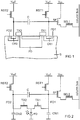
- FIG. 1 shows an example of the pixel structure.
- the circuit of the pixel structure includes a schematical cross section of a semiconductor photodetector device, which can be used for the pixel structure.
- a photodetector PD which may be a pinned photodiode, for example, is integrated in semiconductor material S, in particular in a semiconductor substrate, which may comprise silicon, for instance.
- the photodetector PD can be connected with a first diffusion region FD1 in the semiconductor material S via a first transfer gate TX1 and with a second diffusion region FD2 in the semiconductor material S via a second transfer gate TX2.
- the diffusion regions FD1, FD2 may be arranged on opposite sides of the photodetector PD and may be provided with a first contact region CR1 and a second contact region CR2, respectively.
- the contact regions CR1, CR2 may have a higher doping concentration to enable the formation of an ohmic contact for external electric connections.
- the substrate may be composed of a bulk silicon wafer (e. g. p++ doped) with an epitaxial layer (e. g. p-, 5 ⁇ 10 14 cm -3 ).
- the pinned photodiode may comprise a p++ shallow surface implant and a deeper n-type implant.
- the first contact region CR1 and the second contact region CR2 may be highly doped (e. g. 5 ⁇ 10 19 cm -3 ) n-type implants. They may be surrounded by lower doped n-type implants, and may or may not be located in a p-well area (which may be typically doped with a doping concentration of about 1 ⁇ 10 17 cm -3 ).
- the diffusion regions FD1, FD2 are electrically connected with each other via a capacitor C, which may typically have a capacitance of about 15 fF, for instance.
- the first diffusion region FD1 is also connected to a first reference voltage V ref 1 via a first switch RST1
- the second diffusion region FD2 is also connected to a second reference voltage V ref 2 via a second switch RST2.
- the first and second switches RST1, RST2 can be field-effect transistors, for instance.
- the first reference voltage V ref 1 and the second reference voltage V ref 2 may be equal or different.
- the first diffusion region FD1 is further connected to a buffer amplifier.
- the first diffusion region FD1 may in this case especially be connected to the gate of a further field-effect transistor, for instance.
- the source follower SF connects a supply voltage V DD with a source/drain terminal of a select transistor SEL.
- the other source/drain terminal of the select transistor SEL is connected with a column bus for read-out.
- the supply voltage V DD may in particular be used as the first reference voltage V ref 1 and the second reference voltage V ref 2.
- the source follower SF and the select transistor SEL may also be integrated in the semiconductor material S. Alternatively to the source follower, a junction FET could be used, or a differential amplifier configuration could be used.
- Figure 2 shows a complete circuit diagram of the pixel circuit according to Figure 1 .
- the node of the first diffusion region FD1 has a first parasitic capacitance Cfd1
- the node of the second diffusion region FD2 has a second parasitic capacitance Cfd2. It is advantageous if the parasitic capacitances Cfd1, Cfd2 are equal and as small as possible.
- the capacitance of the capacitor C is considerably larger than the first and second parasitic capacitances Cfd1, Cfd2.
- Typical values of the first and second parasitic capacitances Cfd1 and Cfd2 could be in the range from 1 fF to 4 fF. Techniques could be used to reduce the parasitic capacitances.
- Each of these parasitic capacitances Cfd1 and Cfd2 is composed of the junction capacitance of the diffusion region, the gate-drain overlap capacitance of the transfer gates, the input capacitance of the buffer amplifier and the gate-drain overlap capacitance of the reset transistor.
- the overlap capacitances could be reduced by dedicated implant schemes, e. g. with modifications of dopant concentrations at lightly doped drain areas (LDDs) located adjacent to the gate under the gate spacer region.
- LDDs lightly doped drain areas
- the junction capacitance and junction sidewall capacitance in particular can be changed by reducing the doping of the p-well under the n+ diffusion area, or by using a moderately doped n-type diffusion surrounding the higher doped n++ ohmic contact area.
- the latter is shown in Figure 1 .
- the capacitance of the buffer amplifier can be reduced by the input transistor topology.
- E. g. a buried channel source follower or JFET could be used with lower input capacitance. Both devices have the additional benefit that they have lower 1/f and random-telegraph-signal noise, which is also a benefit to reduce the read noise of the pixel.
- the reference voltages V ref 1 and V ref 2 are choosen such that the signal swing on nodes FD1 and FD2 can be maximized.
- An image with active illumination (e. g. when a structured light pattern is projected) may be integrated using the first diffusion region FD1, while a background reference image may be integrated using the second diffusion region FD2.
- the signal at the first diffusion region FD1 will drop faster than the signal at the second diffusion region FD2.
- the voltage on FD1 will drop below V ref 1 and the voltage on FD2 will rise above V ref 2. It is then beneficial to use a low voltage for V ref 2 and a high voltage for V ref 1.
- Figure 3 shows a timing diagram for this pixel structure.
- the operation of the pixel structure is synchronously performed with the operation of a structured-light projector for multiple image acquisitions in global shutter mode.
- a first image is taken under structured-light conditions.
- the photocarriers from this image exposure are integrated on the photodiodes of the pixel.
- the photodiode is then read out by a charge transfer through the first transfer gate TX1 with the first switch RST1 in its disconnecting state and the second switch RST2 in its connecting state, so that the signal is transferred to the first diffusion region FD1.
- the first diffusion region FD1 is thus floating when the first switch RST1 is in its disconnecting state.
- the diffusion region must be floating when the corresponding transfer gate is operated.
- a further image is taken without structured light.
- the photocarriers are again integrated on the photodiode.
- the photodiode is then read out by a charge transfer though the second transfer gate TX2 with the first switch RST1 in its connecting state and the second switch RST2 in its disconnecting state, so that the signal is transferred to the second diffusion region FD2.
- the first and second switches RST1, RST2 are alternatingly operated to remove the common mode signal corresponding to the background light.
- the first switch RST1 is in its connecting state only when the second switch RST2 is in its disconnecting state and vice versa, in order to prevent the capacitor C from being discharged.
- the driving circuits should guarantee that the RST1 and RST2 signals are nonoverlapping, in order to avoid this discharge. Only at the start of the image acquisition process, both switches are switched on together, in order to reset the capacitor C.
- the differential image is read out from the first diffusion region FD1 using the source follower SF and the select transistor SEL.
- the first switch RST1 is in its disconnecting state
- the second switch RST2 is in its connecting state, so that the second diffusion region FD2 is at least approximately on the second reference voltage V ref 2, and the first diffusion region FD1 provides the stored signal.
- the voltage at the second transfer gate TX2 is higher than the voltage at the first transfer gate TX1, and the second transfer gate TX2 is acting as anti-blooming drain during readout.
- the photodetector PD saturates, excess charge is removed by means of the second transfer gate TX2 and the second switch RST2.
- the second transfer gate TX2 could be in a high state during readout.
- Figure 4 shows a further timing diagram.
- the timing according to this diagram allows to control the maximal amount of charges to be stored on the photodiode. This avoids overflow from the photodetector to the respective diffusion region. This can especially be useful if the illumination is bright.
- Three distinct voltage levels will be needed for the transfer gate control line if this timing diagram is used: a high voltage to enable charge transfer; a low voltage to prohibit overflow of carriers in case when the photodiode is saturated (under strong light conditions) and a middle voltage level to ensure that overflow of carriers at saturation flows thorugh the transfer gate.
- the overflow should happen to the diffusion region where the respective RST switch is in its connecting stage, so that this diffusion region is connected to its respective V ref voltage.
- Figure 4 shows a particular instance of such timing, but slight modifications can be considered that still are according to the described operation.
- FIG. 5 shows a further timing diagram.
- This timing avoids excessive voltage at the second diffusion region FD2 by delaying the rising edge of the first switch RST1. The excessive voltage could otherwise cause leakage through the second switch RST2.
- the timing depends on the different dimensions of the components, including the full-well capacity of the photodiode PD, the capacitance of the capacitor C, and the parasitic capacitances Cfd1 and Cfd2.
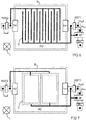
- Figures 6 and 7 show layout examples of the proposed pixel structure, in particular for backside-illuminated image sensor technologies.
- Figure 6 shows an example with a capacitor formed by interdigitated conductor tracks, which can be produced in CMOS technology.
- this capacitor can be arranged on top of the photodetector PD, so that the incident light is not shielded by the conductor tracks.
- An optional reflector R can be provided at the bottom of the layers that are produced in the back end of line (BEOL).
- Figure 7 shows an example with a plate capacitor comprising a sequence of a metal plate, a dielectric layer, and a further metal plate, in particular a metal-isolator-metal (MiM) capacitor, which is known per se.
- the capacitor C is formed by two individual capacitors connected in anti-parallel fashion, in order to keep the parasitic capacitances of the bottom plate identical for the nodes of the first diffusion region FD1 and the second diffusion region FD2.
- capacitors may be appropriate as well, depending on the individual application of the pixel structure. Examples are trench capacitors and polysilicon-insulator-polysilicon capacitors, which are known per se in semiconductor technology.
- Figure 8 shows a structure according to Figure 7 with the difference that the transfer gates TX1, TX2 are located on the same side of the photodetector PD. This arrangement may be advantageous for a more symmetrical pixel layout.
- a separate anti-blooming gate or photodiode reset gate may be connected. It may also be possible to evacuate and overflow charges from the pinned photodiode via a vertical anti-blooming structure. In that case the photodiode can be reset by a voltage pulse on the substrate under the photodiode.
- a two-dimensional array of pixel structures is especially suitable for an image sensor device.
- An imaging system including such an image sensor device may further comprise a light source synchronized to the image sensor device.
- a light source L is schematically indicated in Figures 6 and 7 .
- the light source can be configured to be active when the signal is acquired on the first floating diffusion FD1 and not active when the signal is acquired on the second floating diffusion FD2, or vice versa.
- the light source can be used to project a pattern or a sequence of patterns.
- difference signals are repeatedly obtained by detecting and subtracting two frames, which may be an illuminated frame and a dark frame, for example.
- the difference signals are additively stored.
- the signal-to-noise ratio is increase by charge accumulation. This enables to realize structured-light systems or stereovision with improved tolerance of background light.
- the duration of the corresponding time intervals can be different.
- more than two different frames can be subtracted (e. g. for m different image acquisitions), by use of more than one capacitor in the pixel.
- Each of the frames q i,k , i 1, 2, 3,..., m, can have an exposure time that differs from the exposure times of the other frames.
- Such pixels allow to do charge arithmetic and frame-to-frame calculations in the pixel.
- the subtraction operation can be executed inside the pixel during the image acquisition phase. It is also favourable that, after subtraction, successive acquisitions can be accumulated in the pixel. This improves the saturation level that can be accumulated in the pixel.
- the described pixel structure allows a compact implementation, because it requires only one photodetector, one capacitor, two transfer gates, two reset switches, and a source follower and select transistor in the pixel (6 transistors in total). It is compatible with backside illumination. Different timing allows to store a simple non-subtracted image with large full well charge.
- the described image sensor can also be used in a camera system where an object is tracked. This object is illuminated by a flashed illumination or contains a flashed light source, which is synchronized to the images collected on FD1 or on FD2.
- the described image sensor can also be used in a system where two structured light patterns are projected, and the first structured light pattern is integrated on FD1 while the second structured light pattern is integraded on FD2. This can further enhance the information that can be extracted from the projected patterns.
- Such information could include depth information. This depth information could be calculated from triangulation principles.
- the system could be operated with two light sources at two different wavelengths.
- the eye reflects certain wavelengths and absorbs other wavelengths, leading to a high contrast in a differential image which is the difference between these two images.
- the proposed image sensor pixel allows to generate such profile.
Landscapes
- Engineering & Computer Science (AREA)
- Multimedia (AREA)
- Signal Processing (AREA)
- Physics & Mathematics (AREA)
- Computer Vision & Pattern Recognition (AREA)
- General Physics & Mathematics (AREA)
- Electromagnetism (AREA)
- Solid State Image Pick-Up Elements (AREA)
- Transforming Light Signals Into Electric Signals (AREA)
Abstract
Description
- The present disclosure applies to the field of three-dimensional imaging, especially differential imaging.
- Active stereovision systems make use of a projector and at least one image sensor. Typically the projector projects a structured light pattern that is composed of dots, lines or other shapes which are projected on the scene by infrared light, which may typically have a wavelength of 940 nm, for instance. The pattern is then recorded by a global-shutter two-dimensional image sensor including a two-dimensional matrix of pixels. The image sensor may be optimized for a good response at the used wavelength.
- The light pattern can be projected by a strong light source, such as a VCSEL (vertical-cavity surface-emitting laser) during a short time. The maximum emitted light power is constrained by eye safety limitations and by the maximal power that can be output by the VCSEL at a specified duty cycle. Usually short pulses of few microseconds to few milliseconds are used. A pattern is created, e.g. by a mask, which is projected by an optical system (e.g a lens and/or an optical diffractive element) onto the scene.
- A two-dimensional camera records the projected pattern. The position of the pattern as seen in the recorded image depends on the distance of the objects to the camera and projector. By triangulation the distance can be recorded. Other computation techniques may involve deep learning, for example in a case where the projected patterns changes appearance depending on object distance, thanks to some optical effect like focus distance or interference.
- Some systems use two cameras and employ stereovision to make a depth map. A pattern is projected to create some contrast in the scene. This may be needed for objects without much texture, e.g. a painted wall. In those cases a flashed illumination is used.
- In the above described stereovision and structured light cases, the light is pulsed and illuminated only during short time. The image sensor works in 'global shutter' mode. Before the flash, all pixels are reset and start integrating light. Then the pattern is projected. After the light pulse, the exposure time stops. In the pixels, the signal from the photodiode is sampled on an in-pixel memory. That memory is then read out row-by-row after the exposure time. This is a typical way of operation of global shutter image sensors, in so-called 'triggered global shutter mode'.
- A rolling shutter pixel can instead be used. Because of the significantly larger contribution of background light to the captured signal, fast readout and off-chip data buffer storage are required.
- Background image subtraction can be used to improve the contrast in the image. A second image is captured with the same exposure time but without projected light. The differential image is then calculated by software. The subtraction operation is preferably executed inside the pixel during the image acquisition phase. It is favourable if multiple image acquisitions can be accumulated in the pixel, because a large amount of acquisition cycles enables to enhance the signal-to-noise ratio. After each image acquisition, the signal corresponding to the difference between the images with and without structured light projection remains stored in the pixel. Signals from successive subtraction operations are thus accumulated in the pixel.
- It is an object of the present invention to provide improved differential imaging.
- This object is achieved with the pixel structure for a semiconductor imaging device according to
claim 1, the image sensor device with pixel array according to claim 9 the imaging system according to claim 10, and the method of operating the pixel structure according to claim 13. Embodiments and variants derive from the dependent claims. - The definitions as described above also apply to the following description unless stated otherwise.
- The pixel structure for a semiconductor imaging device comprises a photodetector in a semiconductor material, a first transfer gate between the photodetector and a first diffusion region in the semiconductor material, a second transfer gate between the photodetector and a second diffusion region in the semiconductor material, a capacitor connected between the first diffusion region and the second diffusion region, a first switch connected between the first diffusion region and a first reference voltage, and a second switch connected between the second diffusion region and a second reference voltage.
- In an embodiment of the pixel structure, the photodetector is a pinned photodiode in a substrate comprising the semiconductor material.
- A buffer amplifier is connected to one of the diffusion regions to read out the pixel. In a further embodiment, buffer amplifiers are connected to the first diffusion region and the second diffusion region. In such an embodiment there may also be an additional anti-blooming gate connected to the photodetector to avoid carriers flowing into the diffusion region after the exposures.
- In a further embodiment, the first reference voltage and the second reference voltage are equal, in particular equal to a supply voltage. The first reference voltage or the second reference voltage may be connected to a supply voltage.
- In a further embodiment, a select transistor is connected to a column bus. A source follower formed by a field-effect transistor can be connected to the select transistor, a gate of the source follower being connected to the first diffusion region. This is a possible way of implementing the buffer amplifier.
- The image sensor device comprises a two-dimensional array of such pixel structures.
- The imaging system including such an image sensor device further comprises a light source synchronized to the image sensor device, the light source being configured to be active when the signal is acquired on the first diffusion region and not active when the signal is acquired on the second diffusion region. The light source may instead be configured to be active when the signal is acquired on the second diffusion region and not active when the signal is acquired on the first diffusion region. In particular, the light source can be configured to project a pattern or sequence of patterns on a scene to be imaged.
- The method of operating the pixel structure comprises discharging the capacitor by closing both the first switch and the second switch into a connecting state, acquiring a first signal on the photodetector and transferring the first signal to the first diffusion region by a charge transfer pulse on the first transfer gate, while the second switch is closed in a connecting state, acquiring a second signal on the photodetector and transferring the second signal to the second diffusion region by a charge transfer pulse on the second transfer gate, while the first switch is closed in a connecting state, and after acquisition of the signals, reading the pixel signal out from the first diffusion region while the second diffusion region is connected to the second reference voltage via the second switch.
- In a variant of the method, the second transfer gate is at a higher electric potential than the first transfer gate during readout of the pixel signal.
- Using the method, first and second signals can repeatedly be acquired and accumulated on the capacitor.
- The following is a detailed description of examples of the pixel structure in conjunction with the appended figures.
- Figure 1
- shows a pixel circuit including a schematical cross section of a pinned photodiode.
- Figure 2
- shows a circuit diagram of the pixel circuit according to
Figure 1 . - Figure 3
- is a timing diagram for the pixel structure.
- Figure 4
- is a timing diagram according to
Figure 3 for control of the maximal amount of stored charges. - Figure 5
- is an alternative timing diagram according to
Figure 3 for voltage control. - Figure 6
- is a layout example with a capacitor comprising interdigitated conductor tracks.
- Figure 7
- is a layout example with a plate capacitor.
- Figure 8
- is a layout example with a plate capacitor and both transfer gates on the same side.
-
Figure 1 shows an example of the pixel structure. The circuit of the pixel structure includes a schematical cross section of a semiconductor photodetector device, which can be used for the pixel structure. A photodetector PD, which may be a pinned photodiode, for example, is integrated in semiconductor material S, in particular in a semiconductor substrate, which may comprise silicon, for instance. The photodetector PD can be connected with a first diffusion region FD1 in the semiconductor material S via a first transfer gate TX1 and with a second diffusion region FD2 in the semiconductor material S via a second transfer gate TX2. The diffusion regions FD1, FD2 may be arranged on opposite sides of the photodetector PD and may be provided with a first contact region CR1 and a second contact region CR2, respectively. The contact regions CR1, CR2 may have a higher doping concentration to enable the formation of an ohmic contact for external electric connections. - Typically the substrate may be composed of a bulk silicon wafer (e. g. p++ doped) with an epitaxial layer (e. g. p-, 5×1014 cm-3). The pinned photodiode may comprise a p++ shallow surface implant and a deeper n-type implant. The first contact region CR1 and the second contact region CR2 may be highly doped (e. g. 5×1019 cm-3) n-type implants. They may be surrounded by lower doped n-type implants, and may or may not be located in a p-well area (which may be typically doped with a doping concentration of about 1×1017 cm-3).
- The diffusion regions FD1, FD2 are electrically connected with each other via a capacitor C, which may typically have a capacitance of about 15 fF, for instance. The first diffusion region FD1 is also connected to a first
reference voltage V ref1 via a first switch RST1, and the second diffusion region FD2 is also connected to a secondreference voltage V ref2 via a second switch RST2. The first and second switches RST1, RST2 can be field-effect transistors, for instance. The firstreference voltage V ref1 and the secondreference voltage V ref2 may be equal or different. - The first diffusion region FD1 is further connected to a buffer amplifier. This could be a source follower SF as shown in
Figure 1 . The first diffusion region FD1 may in this case especially be connected to the gate of a further field-effect transistor, for instance. The source follower SF connects a supply voltage VDD with a source/drain terminal of a select transistor SEL. The other source/drain terminal of the select transistor SEL is connected with a column bus for read-out. The supply voltage VDD may in particular be used as the firstreference voltage V ref1 and the secondreference voltage V ref2. The source follower SF and the select transistor SEL may also be integrated in the semiconductor material S. Alternatively to the source follower, a junction FET could be used, or a differential amplifier configuration could be used. -
Figure 2 shows a complete circuit diagram of the pixel circuit according toFigure 1 . The node of the first diffusion region FD1 has a first parasitic capacitance Cfd1, and the node of the second diffusion region FD2 has a second parasitic capacitance Cfd2. It is advantageous if the parasitic capacitances Cfd1, Cfd2 are equal and as small as possible. The capacitance of the capacitor C is considerably larger than the first and second parasitic capacitances Cfd1, Cfd2. Typical values of the first and second parasitic capacitances Cfd1 and Cfd2 could be in the range from 1 fF to 4 fF. Techniques could be used to reduce the parasitic capacitances. Each of these parasitic capacitances Cfd1 and Cfd2 is composed of the junction capacitance of the diffusion region, the gate-drain overlap capacitance of the transfer gates, the input capacitance of the buffer amplifier and the gate-drain overlap capacitance of the reset transistor. The overlap capacitances could be reduced by dedicated implant schemes, e. g. with modifications of dopant concentrations at lightly doped drain areas (LDDs) located adjacent to the gate under the gate spacer region. The junction capacitance and junction sidewall capacitance in particular can be changed by reducing the doping of the p-well under the n+ diffusion area, or by using a moderately doped n-type diffusion surrounding the higher doped n++ ohmic contact area. The latter is shown inFigure 1 . The capacitance of the buffer amplifier can be reduced by the input transistor topology. E. g. a buried channel source follower or JFET could be used with lower input capacitance. Both devices have the additional benefit that they have lower 1/f and random-telegraph-signal noise, which is also a benefit to reduce the read noise of the pixel. - Charges are dumped for successive frames consecutively on the first diffusion region FD1, while the second diffusion region FD2 is kept at the second
reference voltage V ref2 via the second switch RST2, and on the second diffusion region FD2, while the first diffusion region FD1 is kept at the firstreference voltage V ref1 via the first switch RST1. Thereference voltages V ref1 andV ref2 are choosen such that the signal swing on nodes FD1 and FD2 can be maximized. - An image with active illumination (e. g. when a structured light pattern is projected) may be integrated using the first diffusion region FD1, while a background reference image may be integrated using the second diffusion region FD2. In this case the signal at the first diffusion region FD1 will drop faster than the signal at the second diffusion region FD2. After several acquisitions of illuminated and background reference images, as per the later described timing diagrams, where the illuminated image is always transferred to FD1 and the background reference voltage is always transferred to FD2, the voltage on FD1 will drop below
V ref1 and the voltage on FD2 will rise aboveV ref2. It is then beneficial to use a low voltage forV ref2 and a high voltage forV ref1. It should be ensured that the voltage levels on FD1 and FD2 are always higher than the depletion voltage of the pinned photodiode at the moment that the respective transfer gate TX1 or TX2 is opened. This is needed to guarantee a charge transfer of all carriers from the photodiode to the nodes FD1 and FD2. -
Figure 3 shows a timing diagram for this pixel structure. The operation of the pixel structure is synchronously performed with the operation of a structured-light projector for multiple image acquisitions in global shutter mode. A first image is taken under structured-light conditions. The photocarriers from this image exposure are integrated on the photodiodes of the pixel. The photodiode is then read out by a charge transfer through the first transfer gate TX1 with the first switch RST1 in its disconnecting state and the second switch RST2 in its connecting state, so that the signal is transferred to the first diffusion region FD1. The first diffusion region FD1 is thus floating when the first switch RST1 is in its disconnecting state. The diffusion region must be floating when the corresponding transfer gate is operated. A further image is taken without structured light. The photocarriers are again integrated on the photodiode. The photodiode is then read out by a charge transfer though the second transfer gate TX2 with the first switch RST1 in its connecting state and the second switch RST2 in its disconnecting state, so that the signal is transferred to the second diffusion region FD2. - The first and second switches RST1, RST2 are alternatingly operated to remove the common mode signal corresponding to the background light. The first switch RST1 is in its connecting state only when the second switch RST2 is in its disconnecting state and vice versa, in order to prevent the capacitor C from being discharged. The driving circuits should guarantee that the RST1 and RST2 signals are nonoverlapping, in order to avoid this discharge. Only at the start of the image acquisition process, both switches are switched on together, in order to reset the capacitor C.
- After the time period of exposure, the differential image is read out from the first diffusion region FD1 using the source follower SF and the select transistor SEL. For this purpose, the first switch RST1 is in its disconnecting state, and the second switch RST2 is in its connecting state, so that the second diffusion region FD2 is at least approximately on the second
reference voltage V ref2, and the first diffusion region FD1 provides the stored signal. The voltage at the second transfer gate TX2 is higher than the voltage at the first transfer gate TX1, and the second transfer gate TX2 is acting as anti-blooming drain during readout. When the photodetector PD saturates, excess charge is removed by means of the second transfer gate TX2 and the second switch RST2. Alternatively, the second transfer gate TX2 could be in a high state during readout. -
Figure 4 shows a further timing diagram. The timing according to this diagram allows to control the maximal amount of charges to be stored on the photodiode. This avoids overflow from the photodetector to the respective diffusion region. This can especially be useful if the illumination is bright. Three distinct voltage levels will be needed for the transfer gate control line if this timing diagram is used: a high voltage to enable charge transfer; a low voltage to prohibit overflow of carriers in case when the photodiode is saturated (under strong light conditions) and a middle voltage level to ensure that overflow of carriers at saturation flows thorugh the transfer gate. The overflow should happen to the diffusion region where the respective RST switch is in its connecting stage, so that this diffusion region is connected to its respective Vref voltage.Figure 4 shows a particular instance of such timing, but slight modifications can be considered that still are according to the described operation. -
Figure 5 shows a further timing diagram. This timing avoids excessive voltage at the second diffusion region FD2 by delaying the rising edge of the first switch RST1. The excessive voltage could otherwise cause leakage through the second switch RST2. The timing depends on the different dimensions of the components, including the full-well capacity of the photodiode PD, the capacitance of the capacitor C, and the parasitic capacitances Cfd1 and Cfd2. -
Figures 6 and 7 show layout examples of the proposed pixel structure, in particular for backside-illuminated image sensor technologies. -
Figure 6 shows an example with a capacitor formed by interdigitated conductor tracks, which can be produced in CMOS technology. For backside illumination, this capacitor can be arranged on top of the photodetector PD, so that the incident light is not shielded by the conductor tracks. An optional reflector R can be provided at the bottom of the layers that are produced in the back end of line (BEOL). -
Figure 7 shows an example with a plate capacitor comprising a sequence of a metal plate, a dielectric layer, and a further metal plate, in particular a metal-isolator-metal (MiM) capacitor, which is known per se. In the example shown inFigure 7 , the capacitor C is formed by two individual capacitors connected in anti-parallel fashion, in order to keep the parasitic capacitances of the bottom plate identical for the nodes of the first diffusion region FD1 and the second diffusion region FD2. - Other types of capacitors may be appropriate as well, depending on the individual application of the pixel structure. Examples are trench capacitors and polysilicon-insulator-polysilicon capacitors, which are known per se in semiconductor technology.
-
Figure 8 shows a structure according toFigure 7 with the difference that the transfer gates TX1, TX2 are located on the same side of the photodetector PD. This arrangement may be advantageous for a more symmetrical pixel layout. - Additionally, a separate anti-blooming gate or photodiode reset gate may be connected. It may also be possible to evacuate and overflow charges from the pinned photodiode via a vertical anti-blooming structure. In that case the photodiode can be reset by a voltage pulse on the substrate under the photodiode.
- A two-dimensional array of pixel structures is especially suitable for an image sensor device. An imaging system including such an image sensor device may further comprise a light source synchronized to the image sensor device. A light source L is schematically indicated in
Figures 6 and 7 . The light source can be configured to be active when the signal is acquired on the first floating diffusion FD1 and not active when the signal is acquired on the second floating diffusion FD2, or vice versa. The light source can be used to project a pattern or a sequence of patterns. - In typical applications of the described pixel structure, difference signals are repeatedly obtained by detecting and subtracting two frames, which may be an illuminated frame and a dark frame, for example. The difference signals are additively stored. Thus the signal-to-noise ratio is increase by charge accumulation. This enables to realize structured-light systems or stereovision with improved tolerance of background light. The amount of accumulated photocharges is

frame number 1, which may be an illuminated frame, for example, andframe number 2, which may be a dark frame. The duration of the corresponding time intervals can be different. - In embodiments of the pixel structure, more than two different frames can be subtracted (e. g. for m different image acquisitions), by use of more than one capacitor in the pixel. Each of the frames qi,k, i = 1, 2, 3,..., m, can have an exposure time that differs from the exposure times of the other frames. Such pixels allow to do charge arithmetic and frame-to-frame calculations in the pixel.
- It is advantageous that the subtraction operation can be executed inside the pixel during the image acquisition phase. It is also favourable that, after subtraction, successive acquisitions can be accumulated in the pixel. This improves the saturation level that can be accumulated in the pixel. The described pixel structure allows a compact implementation, because it requires only one photodetector, one capacitor, two transfer gates, two reset switches, and a source follower and select transistor in the pixel (6 transistors in total). It is compatible with backside illumination. Different timing allows to store a simple non-subtracted image with large full well charge.
- The described image sensor can also be used in a camera system where an object is tracked. This object is illuminated by a flashed illumination or contains a flashed light source, which is synchronized to the images collected on FD1 or on FD2.
- The described image sensor can also be used in a system where two structured light patterns are projected, and the first structured light pattern is integrated on FD1 while the second structured light pattern is integraded on FD2. This can further enhance the information that can be extracted from the projected patterns. Such information could include depth information. This depth information could be calculated from triangulation principles.
- Similarly, the system could be operated with two light sources at two different wavelengths. E. g. for eye tracking applications, it is known that the eye reflects certain wavelengths and absorbs other wavelengths, leading to a high contrast in a differential image which is the difference between these two images. The proposed image sensor pixel allows to generate such profile.
-
- C
- capacitor
- Cfd1
- first parasitic capacitance
- Cfd2
- second parasitic capacitance
- CR1
- first contact region
- CR2
- second contact region
- FD1
- first diffusion region
- FD2
- second diffusion region
- L
- light source
- PD
- photodetector
- R
- reflector
- RST1
- first switch
- RST2
- second switch
- S
- substrate
- SEL
- select transistor
- SF
- source follower
- TX1
- first transfer gate
- TX2
- second transfer gate
- VDD
- supply voltage
-
V ref1 - first reference voltage
-
V ref2 - second reference voltage
Claims (14)
- A pixel structure for a semiconductor imaging device, comprising:a photodetector (PD) in a semiconductor material (S),a first transfer gate (TX1) between the photodetector (PD) and a first diffusion region (FD1) in the semiconductor material,a second transfer gate (TX2) between the photodetector (PD) and a second diffusion region (FD2) in the semiconductor material,a capacitor (C) connected between the first diffusion region (FD1) and the second diffusion region (FD2),a first switch (RST1) connected between the first diffusion region (FD1) and a first reference voltage (Vref1), anda second switch (RST1) connected between the second diffusion region (FD2) and a second reference voltage (Vref2).
- The pixel structure according to claim 1, wherein
the photodetector (PD) is a pinned photodiode in a substrate comprising the semiconductor material (S). - The pixel structure according to claim 1 or 2, further comprising:buffer amplifiers connected to the first diffusion region (FD1) and the second diffusion region (FD2).
- The pixel structure according to one of claims 1 to 3, wherein the first reference voltage (Vref1) and the second reference voltage (Vref2) are equal.
- The pixel structure according to claim 4, wherein the first reference voltage (Vref1) and the second reference voltage (Vref2) are equal to a supply voltage (VDD).
- The pixel structure according to one of claims 1 to3, wherein the first reference voltage (Vref1) or the second reference voltage (Vref2) is connected to a supply voltage (VDD).
- The pixel structure according to one of claims 1 to 6, further comprising:a select transistor (SEL) connected to a column bus.
- The pixel structure according to claim 7, further comprising:a source follower (SF) formed by a field-effect transistor, which is connected to the select transistor (SEL), a gate of the source follower (SF) being connected to the first diffusion region (FD1).
- An image sensor device comprising a two-dimensional array of pixel structures according to one of claims 1 to 8.
- An imaging system including an image sensor device according to claim 9, further comprising:a light source (L) synchronized to the image sensor device, the light source (L) being configured to be active when the signal is acquired on the first diffusion region (FD1) and not active when the signal is acquired on the second diffusion region (FD2), or vice versa.
- The imaging system according to claim 10, wherein the light source (L) is configured to project a pattern or sequence of patterns on a scene to be imaged.
- A method of operating the pixel structure according to one of claims 1 to 8, comprising:discharging the capacitor (C) by closing both the first switch (RST1) and the second switch (RST2) into a connecting state,acquiring a first signal on the photodetector (PD) and transferring the first signal to the first diffusion region (FD1) by a charge transfer pulse on the first transfer gate (TX1), while the second switch (RST2) is closed in a connecting state,acquiring a second signal on the photodetector (PD) and transferring the second signal to the second diffusion region (FD2) by a charge transfer pulse on the second transfer gate (TX2), while the first switch (RST1) is closed in a connecting state, andafter acquisition of the signals, reading the pixel signal out from the first diffusion region (FD1) while the second diffusion region (FD2) is connected to the second reference voltage (Vref2) via the second switch (RST2).
- The method according to claim 12, wherein
the second transfer gate (TX2) is at a higher electric potential than the first transfer gate (TX2) during readout of the pixel signal. - The method according to claim 12 or 13, wherein
first and second signals are repeatedly acquired and accumulated on the capacitor (C).
Priority Applications (6)
| Application Number | Priority Date | Filing Date | Title |
|---|---|---|---|
| EP17207772.9A EP3499872B1 (en) | 2017-12-15 | 2017-12-15 | Pixel structure, image sensor device and system with pixel structure, and method of operating the pixel structure |
| CN201880073125.3A CN111684791B (en) | 2017-12-15 | 2018-12-10 | Pixel structure, image sensor device and system having pixel structure, and method of operating same |
| US16/771,288 US11405602B2 (en) | 2017-12-15 | 2018-12-10 | Pixel structure, image sensor device and system with pixel structure, and method of operating the pixel structure |
| PCT/EP2018/084188 WO2019115459A1 (en) | 2017-12-15 | 2018-12-10 | Pixel structure, image sensor device and system with pixel structure, and method of operating the pixel structure |
| TW107144794A TWI837107B (en) | 2017-12-15 | 2018-12-12 | Pixel structure, image sensor device and system with pixel structure, and method of operating the pixel structure |
| US17/847,573 US20220321862A1 (en) | 2017-12-15 | 2022-06-23 | Pixel structure, image sensor device and system with pixel structure, and method of operating the pixel structure |
Applications Claiming Priority (1)
| Application Number | Priority Date | Filing Date | Title |
|---|---|---|---|
| EP17207772.9A EP3499872B1 (en) | 2017-12-15 | 2017-12-15 | Pixel structure, image sensor device and system with pixel structure, and method of operating the pixel structure |
Publications (2)
| Publication Number | Publication Date |
|---|---|
| EP3499872A1 true EP3499872A1 (en) | 2019-06-19 |
| EP3499872B1 EP3499872B1 (en) | 2020-08-19 |
Family
ID=60923258
Family Applications (1)
| Application Number | Title | Priority Date | Filing Date |
|---|---|---|---|
| EP17207772.9A Active EP3499872B1 (en) | 2017-12-15 | 2017-12-15 | Pixel structure, image sensor device and system with pixel structure, and method of operating the pixel structure |
Country Status (5)
| Country | Link |
|---|---|
| US (2) | US11405602B2 (en) |
| EP (1) | EP3499872B1 (en) |
| CN (1) | CN111684791B (en) |
| TW (1) | TWI837107B (en) |
| WO (1) | WO2019115459A1 (en) |
Cited By (1)
| Publication number | Priority date | Publication date | Assignee | Title |
|---|---|---|---|---|
| WO2021054183A1 (en) * | 2019-09-18 | 2021-03-25 | Sony Semiconductor Solutions Corporation | Solid-state imaging device and imaging device with combined dynamic vision sensor and imaging functions |
Families Citing this family (6)
| Publication number | Priority date | Publication date | Assignee | Title |
|---|---|---|---|---|
| EP3499872B1 (en) * | 2017-12-15 | 2020-08-19 | ams AG | Pixel structure, image sensor device and system with pixel structure, and method of operating the pixel structure |
| KR102880110B1 (en) * | 2020-03-16 | 2025-11-03 | 에스케이하이닉스 주식회사 | Image sensing device and operating method of the same |
| JP2022000873A (en) * | 2020-06-19 | 2022-01-04 | ソニーセミコンダクタソリューションズ株式会社 | Solid-state image sensor |
| CN114079709B (en) * | 2020-08-07 | 2024-04-12 | 安霸国际有限合伙企业 | Driver mechanism for rolling shutter sensor to acquire structured light patterns |
| US12328519B2 (en) * | 2022-02-15 | 2025-06-10 | Novatek Microelectronics Corp. | Image sensor |
| CN115206940B (en) * | 2022-06-30 | 2024-11-29 | 上海韦尔半导体股份有限公司 | A test structure and test method for potential analysis of interdigitated photodiodes |
Citations (5)
| Publication number | Priority date | Publication date | Assignee | Title |
|---|---|---|---|---|
| US20040013232A1 (en) * | 2002-07-17 | 2004-01-22 | Jeffrey Rahn | Pixel circuitry for imaging system |
| US20080079833A1 (en) * | 2006-09-29 | 2008-04-03 | Brainvision Inc. | Solid-state image sensor |
| US20100308209A1 (en) * | 2009-06-09 | 2010-12-09 | Mesa Imaging Ag | System for Charge-Domain Electron Subtraction in Demodulation Pixels and Method Therefor |
| EP2541275A1 (en) * | 2010-02-26 | 2013-01-02 | Hamamatsu Photonics K.K. | Range image sensor |
| US20140240692A1 (en) * | 2013-02-26 | 2014-08-28 | An-chun Tien | Time-of-flight (tof) system, sensor pixel, and method |
Family Cites Families (14)
| Publication number | Priority date | Publication date | Assignee | Title |
|---|---|---|---|---|
| JP2736121B2 (en) | 1989-07-12 | 1998-04-02 | 株式会社東芝 | Charge transfer device and solid-state imaging device |
| WO2004093318A2 (en) | 2003-04-11 | 2004-10-28 | Canesta, Inc. | Method and system to differentially enhance sensor dynamic range |
| KR100830583B1 (en) | 2006-11-13 | 2008-05-22 | 삼성전자주식회사 | Pixel circuit of the CMOS image sensor capable of dual capture and its structure |
| JP4420039B2 (en) * | 2007-02-16 | 2010-02-24 | ソニー株式会社 | Solid-state imaging device |
| EP2109306B1 (en) | 2008-04-07 | 2015-03-11 | CMOSIS nv | Pixel array with global shutter |
| GB2477083A (en) | 2010-01-13 | 2011-07-27 | Cmosis Nv | Pixel structure with multiple transfer gates to improve dynamic range |
| JP2011204878A (en) | 2010-03-25 | 2011-10-13 | Sony Corp | Solid-state image pickup device and electronic equipment |
| KR101460692B1 (en) | 2011-06-09 | 2014-11-13 | 삼성전자주식회사 | Apparatus for driving 2 dimensional transducer-array, medical imaging system and method for driving 2 dimensional transducer-array |
| KR101900273B1 (en) * | 2011-07-15 | 2018-09-21 | 삼성전자 주식회사 | Cmos image sensor |
| US9832407B2 (en) * | 2014-11-26 | 2017-11-28 | Semiconductor Components Industries, Llc | Global shutter image sensor pixels having improved shutter efficiency |
| JP6395651B2 (en) | 2015-03-30 | 2018-09-26 | 株式会社ジャパンディスプレイ | Input device and display device |
| US10680021B2 (en) * | 2017-05-12 | 2020-06-09 | General Electric Company | Active pixel sensor computed tomography (CT) detector and method of readout |
| EP3499872B1 (en) * | 2017-12-15 | 2020-08-19 | ams AG | Pixel structure, image sensor device and system with pixel structure, and method of operating the pixel structure |
| CN108270981B (en) * | 2017-12-19 | 2021-05-14 | 思特威(上海)电子科技股份有限公司 | Pixel unit, imaging method and imaging device thereof |
-
2017
- 2017-12-15 EP EP17207772.9A patent/EP3499872B1/en active Active
-
2018
- 2018-12-10 WO PCT/EP2018/084188 patent/WO2019115459A1/en not_active Ceased
- 2018-12-10 CN CN201880073125.3A patent/CN111684791B/en active Active
- 2018-12-10 US US16/771,288 patent/US11405602B2/en active Active
- 2018-12-12 TW TW107144794A patent/TWI837107B/en active
-
2022
- 2022-06-23 US US17/847,573 patent/US20220321862A1/en not_active Abandoned
Patent Citations (5)
| Publication number | Priority date | Publication date | Assignee | Title |
|---|---|---|---|---|
| US20040013232A1 (en) * | 2002-07-17 | 2004-01-22 | Jeffrey Rahn | Pixel circuitry for imaging system |
| US20080079833A1 (en) * | 2006-09-29 | 2008-04-03 | Brainvision Inc. | Solid-state image sensor |
| US20100308209A1 (en) * | 2009-06-09 | 2010-12-09 | Mesa Imaging Ag | System for Charge-Domain Electron Subtraction in Demodulation Pixels and Method Therefor |
| EP2541275A1 (en) * | 2010-02-26 | 2013-01-02 | Hamamatsu Photonics K.K. | Range image sensor |
| US20140240692A1 (en) * | 2013-02-26 | 2014-08-28 | An-chun Tien | Time-of-flight (tof) system, sensor pixel, and method |
Cited By (6)
| Publication number | Priority date | Publication date | Assignee | Title |
|---|---|---|---|---|
| WO2021054183A1 (en) * | 2019-09-18 | 2021-03-25 | Sony Semiconductor Solutions Corporation | Solid-state imaging device and imaging device with combined dynamic vision sensor and imaging functions |
| US11240449B2 (en) | 2019-09-18 | 2022-02-01 | Sony Semiconductor Solutions Corporation | Solid-state imaging device and imaging device with combined dynamic vision sensor and imaging functions |
| CN114365288A (en) * | 2019-09-18 | 2022-04-15 | 索尼半导体解决方案公司 | Solid-state imaging device and imaging apparatus having combined dynamic vision sensor function and imaging function |
| US11758300B2 (en) | 2019-09-18 | 2023-09-12 | Sony Semiconductor Solutions Corporation | Solid-state imaging device and imaging device with combined dynamic vision sensor and imaging functions |
| US12058457B2 (en) | 2019-09-18 | 2024-08-06 | Sony Semiconductor Solutions Corporation | Solid-state imaging device and imaging device with combined dynamic vision sensor and imaging functions |
| US12155944B2 (en) | 2019-09-18 | 2024-11-26 | Sony Semiconductor Solutions Corporation | Solid-state imaging device and imaging device with combined dynamic vision sensor and imaging functions |
Also Published As
| Publication number | Publication date |
|---|---|
| EP3499872B1 (en) | 2020-08-19 |
| WO2019115459A1 (en) | 2019-06-20 |
| TWI837107B (en) | 2024-04-01 |
| US11405602B2 (en) | 2022-08-02 |
| US20200382762A1 (en) | 2020-12-03 |
| CN111684791B (en) | 2022-12-09 |
| TW201931618A (en) | 2019-08-01 |
| CN111684791A (en) | 2020-09-18 |
| US20220321862A1 (en) | 2022-10-06 |
Similar Documents
| Publication | Publication Date | Title |
|---|---|---|
| US20220321862A1 (en) | Pixel structure, image sensor device and system with pixel structure, and method of operating the pixel structure | |
| US7286174B1 (en) | Dual storage node pixel for CMOS sensor | |
| US9602750B2 (en) | Image sensor pixels having built-in variable gain feedback amplifier circuitry | |
| ES2901214T3 (en) | Time-of-Flight Image Pixel Readout Voltage Uncertainty Compensation | |
| US7952635B2 (en) | Low noise readout apparatus and method with snapshot shutter and correlated double sampling | |
| CN111466029B (en) | Global shutter pixel circuit and method for computer vision applications | |
| US10630928B2 (en) | Image sensor pixels with overflow capabilities | |
| US10848695B2 (en) | Solid state imaging device, imaging system, and manufacturing method of solid state imaging device | |
| US10690755B2 (en) | Solid-state imaging device having increased distance measurement accuracy and increased distance measurement range | |
| US10616519B2 (en) | Global shutter pixel structures with shared transfer gates | |
| US8792087B2 (en) | Concept for optical distance measurement | |
| US10453879B2 (en) | Solid-state imaging device, imaging system, and movable object | |
| US9455295B2 (en) | Solid-state image sensor with MOS capacitor storage section to which a negative bias is applied after a reset sampling period and electronic device incorporating same | |
| US20120200752A1 (en) | Solid-state image pickup device | |
| US20090224139A1 (en) | Drift Field Demodulation Pixel with Pinned Photo Diode | |
| CN108270981B (en) | Pixel unit, imaging method and imaging device thereof | |
| US20050110093A1 (en) | Anti-blooming storage pixel | |
| US10666875B2 (en) | Solid-state imaging device | |
| US20100308209A1 (en) | System for Charge-Domain Electron Subtraction in Demodulation Pixels and Method Therefor | |
| KR20160001918U (en) | Global shutter image sensor pixels having improved shutter efficiency | |
| KR20080113398A (en) | Method and apparatus for providing rolling double reset timing for global storage of image sensor | |
| KR20090086074A (en) | Image sensor and camera | |
| EP3930309A1 (en) | Pixel and method for operating a pixel | |
| EP3420592B1 (en) | Improved ultra-high dynamic range pixel architecture | |
| KR20210064687A (en) | Image Sensor |
Legal Events
| Date | Code | Title | Description |
|---|---|---|---|
| PUAI | Public reference made under article 153(3) epc to a published international application that has entered the european phase |
Free format text: ORIGINAL CODE: 0009012 |
|
| STAA | Information on the status of an ep patent application or granted ep patent |
Free format text: STATUS: THE APPLICATION HAS BEEN PUBLISHED |
|
| AK | Designated contracting states |
Kind code of ref document: A1 Designated state(s): AL AT BE BG CH CY CZ DE DK EE ES FI FR GB GR HR HU IE IS IT LI LT LU LV MC MK MT NL NO PL PT RO RS SE SI SK SM TR |
|
| AX | Request for extension of the european patent |
Extension state: BA ME |
|
| STAA | Information on the status of an ep patent application or granted ep patent |
Free format text: STATUS: REQUEST FOR EXAMINATION WAS MADE |
|
| 17P | Request for examination filed |
Effective date: 20191120 |
|
| RBV | Designated contracting states (corrected) |
Designated state(s): AL AT BE BG CH CY CZ DE DK EE ES FI FR GB GR HR HU IE IS IT LI LT LU LV MC MK MT NL NO PL PT RO RS SE SI SK SM TR |
|
| GRAP | Despatch of communication of intention to grant a patent |
Free format text: ORIGINAL CODE: EPIDOSNIGR1 |
|
| STAA | Information on the status of an ep patent application or granted ep patent |
Free format text: STATUS: GRANT OF PATENT IS INTENDED |
|
| INTG | Intention to grant announced |
Effective date: 20200401 |
|
| GRAS | Grant fee paid |
Free format text: ORIGINAL CODE: EPIDOSNIGR3 |
|
| GRAA | (expected) grant |
Free format text: ORIGINAL CODE: 0009210 |
|
| STAA | Information on the status of an ep patent application or granted ep patent |
Free format text: STATUS: THE PATENT HAS BEEN GRANTED |
|
| RIN1 | Information on inventor provided before grant (corrected) |
Inventor name: MEYNANTS, GUY |
|
| AK | Designated contracting states |
Kind code of ref document: B1 Designated state(s): AL AT BE BG CH CY CZ DE DK EE ES FI FR GB GR HR HU IE IS IT LI LT LU LV MC MK MT NL NO PL PT RO RS SE SI SK SM TR |
|
| REG | Reference to a national code |
Ref country code: CH Ref legal event code: EP |
|
| REG | Reference to a national code |
Ref country code: DE Ref legal event code: R096 Ref document number: 602017021870 Country of ref document: DE |
|
| REG | Reference to a national code |
Ref country code: AT Ref legal event code: REF Ref document number: 1305282 Country of ref document: AT Kind code of ref document: T Effective date: 20200915 |
|
| REG | Reference to a national code |
Ref country code: IE Ref legal event code: FG4D |
|
| REG | Reference to a national code |
Ref country code: LT Ref legal event code: MG4D |
|
| REG | Reference to a national code |
Ref country code: NL Ref legal event code: MP Effective date: 20200819 |
|
| PG25 | Lapsed in a contracting state [announced via postgrant information from national office to epo] |
Ref country code: GR Free format text: LAPSE BECAUSE OF FAILURE TO SUBMIT A TRANSLATION OF THE DESCRIPTION OR TO PAY THE FEE WITHIN THE PRESCRIBED TIME-LIMIT Effective date: 20201120 Ref country code: BG Free format text: LAPSE BECAUSE OF FAILURE TO SUBMIT A TRANSLATION OF THE DESCRIPTION OR TO PAY THE FEE WITHIN THE PRESCRIBED TIME-LIMIT Effective date: 20201119 Ref country code: FI Free format text: LAPSE BECAUSE OF FAILURE TO SUBMIT A TRANSLATION OF THE DESCRIPTION OR TO PAY THE FEE WITHIN THE PRESCRIBED TIME-LIMIT Effective date: 20200819 Ref country code: SE Free format text: LAPSE BECAUSE OF FAILURE TO SUBMIT A TRANSLATION OF THE DESCRIPTION OR TO PAY THE FEE WITHIN THE PRESCRIBED TIME-LIMIT Effective date: 20200819 Ref country code: NO Free format text: LAPSE BECAUSE OF FAILURE TO SUBMIT A TRANSLATION OF THE DESCRIPTION OR TO PAY THE FEE WITHIN THE PRESCRIBED TIME-LIMIT Effective date: 20201119 Ref country code: HR Free format text: LAPSE BECAUSE OF FAILURE TO SUBMIT A TRANSLATION OF THE DESCRIPTION OR TO PAY THE FEE WITHIN THE PRESCRIBED TIME-LIMIT Effective date: 20200819 Ref country code: PT Free format text: LAPSE BECAUSE OF FAILURE TO SUBMIT A TRANSLATION OF THE DESCRIPTION OR TO PAY THE FEE WITHIN THE PRESCRIBED TIME-LIMIT Effective date: 20201221 Ref country code: LT Free format text: LAPSE BECAUSE OF FAILURE TO SUBMIT A TRANSLATION OF THE DESCRIPTION OR TO PAY THE FEE WITHIN THE PRESCRIBED TIME-LIMIT Effective date: 20200819 |
|
| REG | Reference to a national code |
Ref country code: AT Ref legal event code: MK05 Ref document number: 1305282 Country of ref document: AT Kind code of ref document: T Effective date: 20200819 |
|
| PG25 | Lapsed in a contracting state [announced via postgrant information from national office to epo] |
Ref country code: IS Free format text: LAPSE BECAUSE OF FAILURE TO SUBMIT A TRANSLATION OF THE DESCRIPTION OR TO PAY THE FEE WITHIN THE PRESCRIBED TIME-LIMIT Effective date: 20201219 Ref country code: PL Free format text: LAPSE BECAUSE OF FAILURE TO SUBMIT A TRANSLATION OF THE DESCRIPTION OR TO PAY THE FEE WITHIN THE PRESCRIBED TIME-LIMIT Effective date: 20200819 Ref country code: LV Free format text: LAPSE BECAUSE OF FAILURE TO SUBMIT A TRANSLATION OF THE DESCRIPTION OR TO PAY THE FEE WITHIN THE PRESCRIBED TIME-LIMIT Effective date: 20200819 Ref country code: NL Free format text: LAPSE BECAUSE OF FAILURE TO SUBMIT A TRANSLATION OF THE DESCRIPTION OR TO PAY THE FEE WITHIN THE PRESCRIBED TIME-LIMIT Effective date: 20200819 Ref country code: RS Free format text: LAPSE BECAUSE OF FAILURE TO SUBMIT A TRANSLATION OF THE DESCRIPTION OR TO PAY THE FEE WITHIN THE PRESCRIBED TIME-LIMIT Effective date: 20200819 |
|
| PG25 | Lapsed in a contracting state [announced via postgrant information from national office to epo] |
Ref country code: SM Free format text: LAPSE BECAUSE OF FAILURE TO SUBMIT A TRANSLATION OF THE DESCRIPTION OR TO PAY THE FEE WITHIN THE PRESCRIBED TIME-LIMIT Effective date: 20200819 Ref country code: EE Free format text: LAPSE BECAUSE OF FAILURE TO SUBMIT A TRANSLATION OF THE DESCRIPTION OR TO PAY THE FEE WITHIN THE PRESCRIBED TIME-LIMIT Effective date: 20200819 Ref country code: CZ Free format text: LAPSE BECAUSE OF FAILURE TO SUBMIT A TRANSLATION OF THE DESCRIPTION OR TO PAY THE FEE WITHIN THE PRESCRIBED TIME-LIMIT Effective date: 20200819 Ref country code: DK Free format text: LAPSE BECAUSE OF FAILURE TO SUBMIT A TRANSLATION OF THE DESCRIPTION OR TO PAY THE FEE WITHIN THE PRESCRIBED TIME-LIMIT Effective date: 20200819 Ref country code: RO Free format text: LAPSE BECAUSE OF FAILURE TO SUBMIT A TRANSLATION OF THE DESCRIPTION OR TO PAY THE FEE WITHIN THE PRESCRIBED TIME-LIMIT Effective date: 20200819 |
|
| REG | Reference to a national code |
Ref country code: DE Ref legal event code: R097 Ref document number: 602017021870 Country of ref document: DE |
|
| PG25 | Lapsed in a contracting state [announced via postgrant information from national office to epo] |
Ref country code: ES Free format text: LAPSE BECAUSE OF FAILURE TO SUBMIT A TRANSLATION OF THE DESCRIPTION OR TO PAY THE FEE WITHIN THE PRESCRIBED TIME-LIMIT Effective date: 20200819 Ref country code: AL Free format text: LAPSE BECAUSE OF FAILURE TO SUBMIT A TRANSLATION OF THE DESCRIPTION OR TO PAY THE FEE WITHIN THE PRESCRIBED TIME-LIMIT Effective date: 20200819 Ref country code: AT Free format text: LAPSE BECAUSE OF FAILURE TO SUBMIT A TRANSLATION OF THE DESCRIPTION OR TO PAY THE FEE WITHIN THE PRESCRIBED TIME-LIMIT Effective date: 20200819 |
|
| PLBE | No opposition filed within time limit |
Free format text: ORIGINAL CODE: 0009261 |
|
| STAA | Information on the status of an ep patent application or granted ep patent |
Free format text: STATUS: NO OPPOSITION FILED WITHIN TIME LIMIT |
|
| PG25 | Lapsed in a contracting state [announced via postgrant information from national office to epo] |
Ref country code: SK Free format text: LAPSE BECAUSE OF FAILURE TO SUBMIT A TRANSLATION OF THE DESCRIPTION OR TO PAY THE FEE WITHIN THE PRESCRIBED TIME-LIMIT Effective date: 20200819 |
|
| 26N | No opposition filed |
Effective date: 20210520 |
|
| PG25 | Lapsed in a contracting state [announced via postgrant information from national office to epo] |
Ref country code: IT Free format text: LAPSE BECAUSE OF FAILURE TO SUBMIT A TRANSLATION OF THE DESCRIPTION OR TO PAY THE FEE WITHIN THE PRESCRIBED TIME-LIMIT Effective date: 20200819 |
|
| REG | Reference to a national code |
Ref country code: CH Ref legal event code: PL |
|
| PG25 | Lapsed in a contracting state [announced via postgrant information from national office to epo] |
Ref country code: MC Free format text: LAPSE BECAUSE OF FAILURE TO SUBMIT A TRANSLATION OF THE DESCRIPTION OR TO PAY THE FEE WITHIN THE PRESCRIBED TIME-LIMIT Effective date: 20200819 Ref country code: SI Free format text: LAPSE BECAUSE OF FAILURE TO SUBMIT A TRANSLATION OF THE DESCRIPTION OR TO PAY THE FEE WITHIN THE PRESCRIBED TIME-LIMIT Effective date: 20200819 |
|
| REG | Reference to a national code |
Ref country code: BE Ref legal event code: MM Effective date: 20201231 |
|
| PG25 | Lapsed in a contracting state [announced via postgrant information from national office to epo] |
Ref country code: IE Free format text: LAPSE BECAUSE OF NON-PAYMENT OF DUE FEES Effective date: 20201215 Ref country code: LU Free format text: LAPSE BECAUSE OF NON-PAYMENT OF DUE FEES Effective date: 20201215 |
|
| PG25 | Lapsed in a contracting state [announced via postgrant information from national office to epo] |
Ref country code: CH Free format text: LAPSE BECAUSE OF NON-PAYMENT OF DUE FEES Effective date: 20201231 Ref country code: LI Free format text: LAPSE BECAUSE OF NON-PAYMENT OF DUE FEES Effective date: 20201231 |
|
| PG25 | Lapsed in a contracting state [announced via postgrant information from national office to epo] |
Ref country code: TR Free format text: LAPSE BECAUSE OF FAILURE TO SUBMIT A TRANSLATION OF THE DESCRIPTION OR TO PAY THE FEE WITHIN THE PRESCRIBED TIME-LIMIT Effective date: 20200819 Ref country code: MT Free format text: LAPSE BECAUSE OF FAILURE TO SUBMIT A TRANSLATION OF THE DESCRIPTION OR TO PAY THE FEE WITHIN THE PRESCRIBED TIME-LIMIT Effective date: 20200819 Ref country code: CY Free format text: LAPSE BECAUSE OF FAILURE TO SUBMIT A TRANSLATION OF THE DESCRIPTION OR TO PAY THE FEE WITHIN THE PRESCRIBED TIME-LIMIT Effective date: 20200819 |
|
| PG25 | Lapsed in a contracting state [announced via postgrant information from national office to epo] |
Ref country code: MK Free format text: LAPSE BECAUSE OF FAILURE TO SUBMIT A TRANSLATION OF THE DESCRIPTION OR TO PAY THE FEE WITHIN THE PRESCRIBED TIME-LIMIT Effective date: 20200819 |
|
| PG25 | Lapsed in a contracting state [announced via postgrant information from national office to epo] |
Ref country code: BE Free format text: LAPSE BECAUSE OF NON-PAYMENT OF DUE FEES Effective date: 20201231 |
|
| GBPC | Gb: european patent ceased through non-payment of renewal fee |
Effective date: 20211215 |
|
| PG25 | Lapsed in a contracting state [announced via postgrant information from national office to epo] |
Ref country code: GB Free format text: LAPSE BECAUSE OF NON-PAYMENT OF DUE FEES Effective date: 20211215 |
|
| REG | Reference to a national code |
Ref country code: DE Ref legal event code: R079 Ref document number: 602017021870 Country of ref document: DE Free format text: PREVIOUS MAIN CLASS: H04N0005374500 Ipc: H04N0025770000 |
|
| P01 | Opt-out of the competence of the unified patent court (upc) registered |
Effective date: 20230822 |
|
| PGFP | Annual fee paid to national office [announced via postgrant information from national office to epo] |
Ref country code: FR Payment date: 20231222 Year of fee payment: 7 Ref country code: DE Payment date: 20231214 Year of fee payment: 7 |
|
| REG | Reference to a national code |
Ref country code: DE Ref legal event code: R119 Ref document number: 602017021870 Country of ref document: DE |
|
| PG25 | Lapsed in a contracting state [announced via postgrant information from national office to epo] |
Ref country code: DE Free format text: LAPSE BECAUSE OF NON-PAYMENT OF DUE FEES Effective date: 20250701 |
|
| PG25 | Lapsed in a contracting state [announced via postgrant information from national office to epo] |
Ref country code: FR Free format text: LAPSE BECAUSE OF NON-PAYMENT OF DUE FEES Effective date: 20241231 |