EP3499869A1 - Pixel sensing module and image capturing device - Google Patents
Pixel sensing module and image capturing device Download PDFInfo
- Publication number
- EP3499869A1 EP3499869A1 EP17902588.7A EP17902588A EP3499869A1 EP 3499869 A1 EP3499869 A1 EP 3499869A1 EP 17902588 A EP17902588 A EP 17902588A EP 3499869 A1 EP3499869 A1 EP 3499869A1
- Authority
- EP
- European Patent Office
- Prior art keywords
- pixel
- light
- sensing
- sub
- unit
- Prior art date
- Legal status (The legal status is an assumption and is not a legal conclusion. Google has not performed a legal analysis and makes no representation as to the accuracy of the status listed.)
- Granted
Links
Images
Classifications
-
- H—ELECTRICITY
- H10—SEMICONDUCTOR DEVICES; ELECTRIC SOLID-STATE DEVICES NOT OTHERWISE PROVIDED FOR
- H10F—INORGANIC SEMICONDUCTOR DEVICES SENSITIVE TO INFRARED RADIATION, LIGHT, ELECTROMAGNETIC RADIATION OF SHORTER WAVELENGTH OR CORPUSCULAR RADIATION
- H10F39/00—Integrated devices, or assemblies of multiple devices, comprising at least one element covered by group H10F30/00, e.g. radiation detectors comprising photodiode arrays
- H10F39/80—Constructional details of image sensors
- H10F39/802—Geometry or disposition of elements in pixels, e.g. address-lines or gate electrodes
- H10F39/8023—Disposition of the elements in pixels, e.g. smaller elements in the centre of the imager compared to larger elements at the periphery
-
- H—ELECTRICITY
- H04—ELECTRIC COMMUNICATION TECHNIQUE
- H04N—PICTORIAL COMMUNICATION, e.g. TELEVISION
- H04N23/00—Cameras or camera modules comprising electronic image sensors; Control thereof
- H04N23/50—Constructional details
- H04N23/54—Mounting of pick-up tubes, electronic image sensors, deviation or focusing coils
-
- H—ELECTRICITY
- H04—ELECTRIC COMMUNICATION TECHNIQUE
- H04N—PICTORIAL COMMUNICATION, e.g. TELEVISION
- H04N25/00—Circuitry of solid-state image sensors [SSIS]; Control thereof
- H04N25/40—Extracting pixel data from image sensors by controlling scanning circuits, e.g. by modifying the number of pixels sampled or to be sampled
- H04N25/46—Extracting pixel data from image sensors by controlling scanning circuits, e.g. by modifying the number of pixels sampled or to be sampled by combining or binning pixels
-
- H—ELECTRICITY
- H04—ELECTRIC COMMUNICATION TECHNIQUE
- H04N—PICTORIAL COMMUNICATION, e.g. TELEVISION
- H04N25/00—Circuitry of solid-state image sensors [SSIS]; Control thereof
- H04N25/70—SSIS architectures; Circuits associated therewith
- H04N25/76—Addressed sensors, e.g. MOS or CMOS sensors
-
- H—ELECTRICITY
- H10—SEMICONDUCTOR DEVICES; ELECTRIC SOLID-STATE DEVICES NOT OTHERWISE PROVIDED FOR
- H10F—INORGANIC SEMICONDUCTOR DEVICES SENSITIVE TO INFRARED RADIATION, LIGHT, ELECTROMAGNETIC RADIATION OF SHORTER WAVELENGTH OR CORPUSCULAR RADIATION
- H10F39/00—Integrated devices, or assemblies of multiple devices, comprising at least one element covered by group H10F30/00, e.g. radiation detectors comprising photodiode arrays
- H10F39/80—Constructional details of image sensors
- H10F39/806—Optical elements or arrangements associated with the image sensors
- H10F39/8063—Microlenses
-
- H—ELECTRICITY
- H10—SEMICONDUCTOR DEVICES; ELECTRIC SOLID-STATE DEVICES NOT OTHERWISE PROVIDED FOR
- H10F—INORGANIC SEMICONDUCTOR DEVICES SENSITIVE TO INFRARED RADIATION, LIGHT, ELECTROMAGNETIC RADIATION OF SHORTER WAVELENGTH OR CORPUSCULAR RADIATION
- H10F39/00—Integrated devices, or assemblies of multiple devices, comprising at least one element covered by group H10F30/00, e.g. radiation detectors comprising photodiode arrays
- H10F39/80—Constructional details of image sensors
- H10F39/806—Optical elements or arrangements associated with the image sensors
- H10F39/8067—Reflectors
-
- H—ELECTRICITY
- H10—SEMICONDUCTOR DEVICES; ELECTRIC SOLID-STATE DEVICES NOT OTHERWISE PROVIDED FOR
- H10F—INORGANIC SEMICONDUCTOR DEVICES SENSITIVE TO INFRARED RADIATION, LIGHT, ELECTROMAGNETIC RADIATION OF SHORTER WAVELENGTH OR CORPUSCULAR RADIATION
- H10F39/00—Integrated devices, or assemblies of multiple devices, comprising at least one element covered by group H10F30/00, e.g. radiation detectors comprising photodiode arrays
- H10F39/80—Constructional details of image sensors
- H10F39/813—Electronic components shared by multiple pixels, e.g. one amplifier shared by two pixels
-
- H—ELECTRICITY
- H10—SEMICONDUCTOR DEVICES; ELECTRIC SOLID-STATE DEVICES NOT OTHERWISE PROVIDED FOR
- H10F—INORGANIC SEMICONDUCTOR DEVICES SENSITIVE TO INFRARED RADIATION, LIGHT, ELECTROMAGNETIC RADIATION OF SHORTER WAVELENGTH OR CORPUSCULAR RADIATION
- H10F39/00—Integrated devices, or assemblies of multiple devices, comprising at least one element covered by group H10F30/00, e.g. radiation detectors comprising photodiode arrays
- H10F39/10—Integrated devices
- H10F39/12—Image sensors
- H10F39/18—Complementary metal-oxide-semiconductor [CMOS] image sensors; Photodiode array image sensors
-
- H—ELECTRICITY
- H10—SEMICONDUCTOR DEVICES; ELECTRIC SOLID-STATE DEVICES NOT OTHERWISE PROVIDED FOR
- H10F—INORGANIC SEMICONDUCTOR DEVICES SENSITIVE TO INFRARED RADIATION, LIGHT, ELECTROMAGNETIC RADIATION OF SHORTER WAVELENGTH OR CORPUSCULAR RADIATION
- H10F39/00—Integrated devices, or assemblies of multiple devices, comprising at least one element covered by group H10F30/00, e.g. radiation detectors comprising photodiode arrays
- H10F39/80—Constructional details of image sensors
- H10F39/805—Coatings
- H10F39/8057—Optical shielding
Definitions
- the present application relates to a pixel sensing module and an image capturing device, and more particularly, to a pixel sensing module and an image capturing device capable of enhancing light sensitivity.
- CMOS image sensor has been widely applied in electronic devices with image capturing function and digital camera.
- the image sensor comprises a pixel sensing array, and the pixel sensing array comprises a plurality of pixel sensing unit arranged in an array.
- the pixel sensing unit comprises a light-sensing component, such as a photo diode or a photo transistor, and a converting circuit.
- the sensitivity of the pixel sensing unit is related/proportional to a light-sensing area of the light-sensing component.
- the photo diode stores the electronic charges caused by the light in the potential well of the photo diode, and the electronic charges is converted by the converting circuit comprising transistors into voltage signal, where the voltage signal is the pixel value corresponding to the pixel sensing unit.
- Light sensitivity of the pixel sensing unit is related to an area of the photo diode in the circuit layout.
- the pixel sensing unit is required to have a certain light sensing area.
- each pixel sensing unit only comprises a light sensing component.
- the only light sensing component of the pixel sensing unit has to have the required light sensing area of the pixel sensing unit.
- the image sensor comprises a collimator in general, configured to project the light onto the pixel sensing unit.
- the pixel sensing unit and the collimator are not perfectly aligned, such that crosstalk exists between light paths.
- the present application provides pixel sensing module, comprising a pixel light-sensing unit, receiving light at a light receiving side and outputting a pixel value, the pixel light-sensing unit comprising a plurality of sub-pixel light-sensing components, configured to output a plurality of sub-pixel values; and an integrating unit, coupled to the pixel light-sensing unit, configured to output the pixel value according to the plurality of sub-pixel values; and a collimating unit, having a plurality of openings, wherein the plurality of openings are aligned with the area of the pixel light-sensing unit, and projections of the plurality of openings onto the light receiving side lie within an area of the pixel light-sensing unit at the light receiving side.
- a first opening among the plurality of openings is aligned with at least a sub-pixel light-sensing component among the plurality of sub-pixel light-sensing components.
- the plurality of sub-pixel light-sensing components comprises a plurality of light-sensing areas and a plurality of non-light-sensing areas, a projection of the first opening onto the light receiving side coincides with at least a light-sensing area of the at least a sub-pixel light-sensing component.
- the plurality of sub-pixel light-sensing components comprises photo diodes.
- the integrating unit performs an average operation on the plurality of sub-pixel values, to output the pixel value as an average of the plurality of sub-pixel values.
- the integrating unit performs a summation operation on the plurality of sub-pixel values, to output the pixel value as a summation of the plurality of sub-pixel values.
- the integrating unit outputs the pixel value as a sub-pixel value among the plurality of sub-pixel values.
- An embodiment of the present application provides image capturing device comprising a plurality of pixel sensing modules, arranged as an array, wherein each pixel sensing module comprises a pixel light-sensing unit, receiving light at a light receiving side and outputting a pixel value, wherein the pixel light-sensing unit has an area at the light receiving side, the pixel light-sensing unit comprises a plurality of sub-pixel light-sensing components, configured to output a plurality of sub-pixel values; and an integrating unit, coupled to the pixel light-sensing unit, configured to output the pixel value according to the plurality of sub-pixel values; a collimating unit, having a plurality of openings, wherein the plurality of openings are aligned with the area of the pixel light-sensing unit, and projections of the plurality of openings onto the light receiving side lie within the area of the pixel light-sensing unit at the light receiving side.
- the present application utilizes the collimating unit having a plurality of openings aligned with the zone of the pixel light-sensing unit at the light receiving side so as to avoid crosstalk between the light paths and achieve the maximum light amount; and utilizes the plurality of sub-pixel light-sensing components of the pixel light-sensing unit to enhance the draining-out capability.
- the present application arranges the sub-pixel light-sensing components appropriately, such that the projections of the openings at the light receiving side (i.e., the light transmission zone) only overlap with the light-sensing areas of the sub-pixel light-sensing components and do not overlap with the non-light-sensing area of the plurality of sub-pixel light-sensing components, to achieve better light sensitivity.
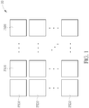
- FIG. 1 is a schematic diagram of an image capturing device 10 according to an embodiment of the present application.
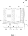
- FIG. 2 is a schematic diagram of a pixel sensing module PXM according to an embodiment of the present application.
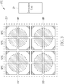
- FIG. 3 is a top view of a pixel light-sensing unit PX according to an embodiment of the present application.
- the image capturing device 10 may be CMOS image sensor (CIS), which may be applied to a device which needs to capture images such as an optical fingerprint identification or a camera.
- the image capturing device 10 comprises a plurality of pixel sensing modules PXM.
- the plurality of pixel sensing modules PXM is arranged as an array.
- the plurality of pixel sensing modules PXM outputs a plurality of pixel values VP corresponding to an image for the backend circuit or the device to perform an image processing or operation(s).
- the pixel sensing module PXM comprises the pixel light-sensing unit PX and a collimating unit CM.
- Each pixel light-sensing unit PX receives light at a light receiving side P1, drains out the photo electronic charges generated by the light, and outputs the pixel value VP corresponding to the pixel light-sensing unit PX.
- the photo electronic charges stored in the pixel light-sensing component are not easily drained out, such that residual electronic charges are left in the light-sensing components, and cause unnecessary image sticking effect on the image capturing device.
- the pixel light-sensing component with large light-sensing area may be partitioned into sub-pixel light-sensing components with small light-sensing area, such that the photo electronic charges are easily drained out.
- the pixel light-sensing unit PX comprises a plurality of sub-pixel light-sensing components SPX and an integrating unit 20. Moreover, if the pixel light-sensing unit PX needs to have a light-sensing area to achieve a certain light sensitivity, a summation of a plurality of sub-light-sensing areas corresponding to the plurality of sub-pixel light-sensing components SPX is substantially the light-sensing area.
- the sub-pixel light-sensing component SPX may comprise a photo diode, which may output a corresponding sub-pixel value SVP.
- the integrating unit 20 is coupled to the plurality of sub-pixel light-sensing components SPX, to receive a plurality of sub-pixel values SVP corresponding to the plurality of sub-pixel light-sensing components SPX.
- the integrating unit 20 is configured to integrate the plurality of sub-pixel values SVP as the pixel value VP. In other words, the integrating unit 20 may output one single pixel value VP according to the plurality of sub-pixel values SVP corresponding to the plurality of sub-pixel light-sensing components SPX.
- the pixel light-sensing unit PX comprises 16 sub-pixel light-sensing components SPX.
- the 16 sub-pixel light-sensing components SPX are all located within a zone ZN at the light receiving side P1 and arranged as a 4 ⁇ 4 array.
- the 16 sub-pixel light-sensing components SPX output 16 sub-pixel values SVP to the integrating unit 20.
- the integrating unit 20 outputs the single pixel value VP according to the 16 sub-pixel values SVP.
- the collimating unit CM may comprise lens LN and a plurality of openings H.
- the opening H is located at a light transmission portion at a bottom of the collimating unit CM.
- light outside the image capturing device 10 may be transmitted through the collimating unit CM and irradiated onto the pixel light-sensing unit PX.
- the plurality of openings H of the collimating unit CM is aligned with the pixel light-sensing unit PX, i.e., projections of the plurality of openings H of the collimating unit CM onto the plane at which the pixel light-sensing unit PX is located (the light receiving side of the pixel light-sensing unit PX) are completely located within the zone ZN of the single pixel light-sensing unit PX at the light receiving side P1.
- the light transmitted through the collimating unit CM would be irradiated onto the pixel light-sensing unit PX, and would not be irradiated on adjacent pixel light-sensing units.
- a projection of the openings H onto the light receiving side P1 is called as a light transmission zone HP.
- a light transmission zone HP For example, in FIG. 3 , 4 light transmission zones HP are illustrated on the 16 sub-pixel light-sensing components SPX. That is, in the current embodiment, the collimating unit CM comprises 4 openings H. Each openings H are aligned to 4 sub-pixel light-sensing components SPX.
- the projection of the each openings H onto the light receiving side P1 i.e., the light transmission zone HP
- the light transmission zone HP is located within the zone ZN of the pixel light-sensing unit PX.
- the plurality of sub-pixel values SVP outputted by the plurality of sub-pixel light-sensing components SPX is corresponding to the single pixel value VP corresponding to the pixel light-sensing unit PX, which means that the light transmitted through the collimating unit CM would not cause crosstalk to the neighboring pixel light-sensing unit, such that the crosstalk between the light paths is avoided.
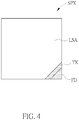
- FIG. 4 is a layout schematic diagram (top view) of a sub-pixel light-sensing component SPX according to an embodiment of the present application.
- the sub-pixel light-sensing component SPX may comprise a light-sensing area LSA, a transmission gate TX and a floating node FD.
- the light-sensing area LSA receives light and produces photo electronic charges.
- the transmission gate TX is configured to apply a signal S TX to drain out the photo electronic charges stored in the light-sensing area LSA to the floating node FD, and the sub-pixel value SVP is related to an amount of the photo electronic charges in the floating node FD of the sub-pixel light-sensing component SPX.
- the light-sensing area LSA receives light and a location of which is related to the light sensitivity of the sub-pixel light-sensing component SPX.
- the transmission gate TX and the floating node FD do not receive light and a location of which is irrelevant to the light sensitivity of the sub-pixel light-sensing component SPX.
- the location of the transmission gate TX and the floating node FD at the light receiving side P1 may be regarded as the non-light-sensing area of the sub-pixel light-sensing component SPX.
- an arrangement of the plurality of sub-pixel light-sensing components SPX of the pixel light-sensing unit PX may be adjusted, such that the light transmission zone HP, the projection of the openings H onto the light receiving side P1 of the pixel light-sensing unit PX, only overlaps with the light-sensing areas LSA of the plurality of sub-pixel light-sensing components SPX, and the light transmission zone HP does not overlap with the non-light-sensing areas of the plurality of sub-pixel light-sensing components SPX. Therefore, the pixel light-sensing unit PX would have better light sensitivity.
- the method of the integrating unit 20 integrating the plurality of sub-pixel values SVP as the pixel value VP is not limited.
- the integrating unit 20 may perform an average operation on the plurality of sub-pixel values SVP, to output the pixel value VP as an average of the plurality of sub-pixel values SVP.
- the integrating unit 20 may perform a summation operation on the plurality of sub-pixel values SVP, to output the pixel value VP as a summation of the plurality of sub-pixel values SVP.
- the integrating unit 20 may choose one sub-pixel value SVP among the plurality of sub-pixel values SVP to be the pixel value VP, and output the pixel value VP as the chosen sub-pixel value SVP.
- the sub-pixel light-sensing components of the pixel light-sensing unit are not limited to be arranged as the 4 ⁇ 4 array.
- the pixel light-sensing unit is not limited to including 16 sub-pixel light-sensing components.
- the sub-pixel light-sensing components within the pixel light-sensing unit may be arranged in different ways, depending on the practical situation, and not limited thereto.
- the present application utilizes the collimating unit having a plurality of openings aligned with the zone of each pixel light-sensing unit at the light receiving side so as to avoid crosstalk between the light paths and achieve the maximum light amount; and utilizes the plurality of sub-pixel light-sensing components of the pixel light-sensing unit to enhance the draining-out capability.
- the present application arranges the sub-pixel light-sensing components appropriately, such that the projections of the openings at the light receiving side (i.e., the light transmission zone) only overlap with the light-sensing areas of the sub-pixel light-sensing components and do not overlap with the non-light-sensing area of the plurality of sub-pixel light-sensing components, to achieve better light sensitivity.
Landscapes
- Engineering & Computer Science (AREA)
- Multimedia (AREA)
- Signal Processing (AREA)
- Solid State Image Pick-Up Elements (AREA)
- Transforming Light Signals Into Electric Signals (AREA)
Abstract
Description
- The present application relates to a pixel sensing module and an image capturing device, and more particularly, to a pixel sensing module and an image capturing device capable of enhancing light sensitivity.
- CMOS image sensor (CIS) has been widely applied in electronic devices with image capturing function and digital camera. In general, the image sensor comprises a pixel sensing array, and the pixel sensing array comprises a plurality of pixel sensing unit arranged in an array. The pixel sensing unit comprises a light-sensing component, such as a photo diode or a photo transistor, and a converting circuit. The sensitivity of the pixel sensing unit is related/proportional to a light-sensing area of the light-sensing component. Take the pixel sensing unit comprising the photo diode as an example, the photo diode stores the electronic charges caused by the light in the potential well of the photo diode, and the electronic charges is converted by the converting circuit comprising transistors into voltage signal, where the voltage signal is the pixel value corresponding to the pixel sensing unit. Light sensitivity of the pixel sensing unit is related to an area of the photo diode in the circuit layout.
- To achieve a specific light sensing capability for the image sensor, the pixel sensing unit is required to have a certain light sensing area. In the prior art, each pixel sensing unit only comprises a light sensing component. In other words, the only light sensing component of the pixel sensing unit has to have the required light sensing area of the pixel sensing unit. However, for the light sensing component with large light sensing area, the electronic charges within the potential well is not easy to be completely drained out by the converting circuit, such that the light-sensing component may have residual electronic charges, which may cause unnecessary image sticking effect on the digital camera. In addition, the image sensor comprises a collimator in general, configured to project the light onto the pixel sensing unit. However, the pixel sensing unit and the collimator are not perfectly aligned, such that crosstalk exists between light paths.
- Therefore, it is necessary to improve the prior art.
- It is therefore an objective of embodiments of the present application to provide a pixel sensing unit and an image capturing device, to improve over disadvantages of the prior art.
- To solve the problem stated in the above, an embodiment of the present application provides, the present application provides pixel sensing module, comprising a pixel light-sensing unit, receiving light at a light receiving side and outputting a pixel value, the pixel light-sensing unit comprising a plurality of sub-pixel light-sensing components, configured to output a plurality of sub-pixel values; and an integrating unit, coupled to the pixel light-sensing unit, configured to output the pixel value according to the plurality of sub-pixel values; and a collimating unit, having a plurality of openings, wherein the plurality of openings are aligned with the area of the pixel light-sensing unit, and projections of the plurality of openings onto the light receiving side lie within an area of the pixel light-sensing unit at the light receiving side.
- For example, a first opening among the plurality of openings is aligned with at least a sub-pixel light-sensing component among the plurality of sub-pixel light-sensing components.
- For example, the plurality of sub-pixel light-sensing components comprises a plurality of light-sensing areas and a plurality of non-light-sensing areas, a projection of the first opening onto the light receiving side coincides with at least a light-sensing area of the at least a sub-pixel light-sensing component.
- For example, the plurality of sub-pixel light-sensing components comprises photo diodes.
- For example, the integrating unit performs an average operation on the plurality of sub-pixel values, to output the pixel value as an average of the plurality of sub-pixel values.
- For example, the integrating unit performs a summation operation on the plurality of sub-pixel values, to output the pixel value as a summation of the plurality of sub-pixel values.
- For example, the integrating unit outputs the pixel value as a sub-pixel value among the plurality of sub-pixel values.
- An embodiment of the present application provides image capturing device comprising a plurality of pixel sensing modules, arranged as an array, wherein each pixel sensing module comprises a pixel light-sensing unit, receiving light at a light receiving side and outputting a pixel value, wherein the pixel light-sensing unit has an area at the light receiving side, the pixel light-sensing unit comprises a plurality of sub-pixel light-sensing components, configured to output a plurality of sub-pixel values; and an integrating unit, coupled to the pixel light-sensing unit, configured to output the pixel value according to the plurality of sub-pixel values; a collimating unit, having a plurality of openings, wherein the plurality of openings are aligned with the area of the pixel light-sensing unit, and projections of the plurality of openings onto the light receiving side lie within the area of the pixel light-sensing unit at the light receiving side.
- The present application utilizes the collimating unit having a plurality of openings aligned with the zone of the pixel light-sensing unit at the light receiving side so as to avoid crosstalk between the light paths and achieve the maximum light amount; and utilizes the plurality of sub-pixel light-sensing components of the pixel light-sensing unit to enhance the draining-out capability. Furthermore, the present application arranges the sub-pixel light-sensing components appropriately, such that the projections of the openings at the light receiving side (i.e., the light transmission zone) only overlap with the light-sensing areas of the sub-pixel light-sensing components and do not overlap with the non-light-sensing area of the plurality of sub-pixel light-sensing components, to achieve better light sensitivity.
- These and other objectives of the present invention will no doubt become obvious to those of ordinary skill in the art after reading the following detailed description of the preferred embodiment that is illustrated in the various figures and drawings.
-
-
FIG. 1 is a schematic diagram of an image capturing device according to an embodiment of the present application; -
FIG. 2 is a side view of a pixel sensing module according to an embodiment of the present application; -
FIG. 3 is a top view of a pixel light-sensing unit according to an embodiment of the present application; -
FIG. 4 is a top view of a sub-pixel light-sensing component according to an embodiment of the present application. - In order to make the objects, technical solutions and advantages of the present application become more apparent, the following relies on the accompanying drawings and embodiments to describe the present application in further detail. It should be understood that the specific embodiments described herein are only for explaining the present application and are not intended to limit the present application.
- Please refer to
FIG. 1 to FIG. 3 .FIG. 1 is a schematic diagram of an image capturingdevice 10 according to an embodiment of the present application.FIG. 2 is a schematic diagram of a pixel sensing module PXM according to an embodiment of the present application.FIG. 3 is a top view of a pixel light-sensing unit PX according to an embodiment of the present application. The image capturingdevice 10 may be CMOS image sensor (CIS), which may be applied to a device which needs to capture images such as an optical fingerprint identification or a camera. As shown inFIG. 1 , theimage capturing device 10 comprises a plurality of pixel sensing modules PXM. The plurality of pixel sensing modules PXM is arranged as an array. The plurality of pixel sensing modules PXM outputs a plurality of pixel values VP corresponding to an image for the backend circuit or the device to perform an image processing or operation(s). - As shown in
FIG. 2 andFIG. 3 , the pixel sensing module PXM comprises the pixel light-sensing unit PX and a collimating unit CM. Each pixel light-sensing unit PX receives light at a light receiving side P1, drains out the photo electronic charges generated by the light, and outputs the pixel value VP corresponding to the pixel light-sensing unit PX. However, for the pixel light-sensing component with large light-sensing area, the photo electronic charges stored in the pixel light-sensing component are not easily drained out, such that residual electronic charges are left in the light-sensing components, and cause unnecessary image sticking effect on the image capturing device. To solve the problem of the residual photo electronic charges, the pixel light-sensing component with large light-sensing area may be partitioned into sub-pixel light-sensing components with small light-sensing area, such that the photo electronic charges are easily drained out. - In detail, the pixel light-sensing unit PX comprises a plurality of sub-pixel light-sensing components SPX and an
integrating unit 20. Moreover, if the pixel light-sensing unit PX needs to have a light-sensing area to achieve a certain light sensitivity, a summation of a plurality of sub-light-sensing areas corresponding to the plurality of sub-pixel light-sensing components SPX is substantially the light-sensing area. The sub-pixel light-sensing component SPX may comprise a photo diode, which may output a corresponding sub-pixel value SVP. The integratingunit 20 is coupled to the plurality of sub-pixel light-sensing components SPX, to receive a plurality of sub-pixel values SVP corresponding to the plurality of sub-pixel light-sensing components SPX. The integratingunit 20 is configured to integrate the plurality of sub-pixel values SVP as the pixel value VP. In other words, the integratingunit 20 may output one single pixel value VP according to the plurality of sub-pixel values SVP corresponding to the plurality of sub-pixel light-sensing components SPX. - Take the pixel light-sensing unit PX illustrated in
FIG. 3 as an example, the pixel light-sensing unit PX comprises 16 sub-pixel light-sensing components SPX. The 16 sub-pixel light-sensing components SPX are all located within a zone ZN at the light receiving side P1 and arranged as a 4×4 array. The 16 sub-pixel light-sensing components SPX output 16 sub-pixel values SVP to theintegrating unit 20. The integratingunit 20 outputs the single pixel value VP according to the 16 sub-pixel values SVP. - In another perspective, the collimating unit CM may comprise lens LN and a plurality of openings H. The opening H is located at a light transmission portion at a bottom of the collimating unit CM. Through the lens LN and the openings H, light outside the
image capturing device 10 may be transmitted through the collimating unit CM and irradiated onto the pixel light-sensing unit PX. In other words, the plurality of openings H of the collimating unit CM is aligned with the pixel light-sensing unit PX, i.e., projections of the plurality of openings H of the collimating unit CM onto the plane at which the pixel light-sensing unit PX is located (the light receiving side of the pixel light-sensing unit PX) are completely located within the zone ZN of the single pixel light-sensing unit PX at the light receiving side P1. In other words, the light transmitted through the collimating unit CM would be irradiated onto the pixel light-sensing unit PX, and would not be irradiated on adjacent pixel light-sensing units. The crosstalk between the light paths is avoided, and a maximum light amount is achieved. A projection of the openings H onto the light receiving side P1 is called as a light transmission zone HP. For example, inFIG. 3 ,4 light transmission zones HP are illustrated on the 16 sub-pixel light-sensing components SPX. That is, in the current embodiment, the collimating unit CM comprises 4 openings H. Each openings H are aligned to 4 sub-pixel light-sensing components SPX. The projection of the each openings H onto the light receiving side P1 (i.e., the light transmission zone HP) is located within the zone ZN of the pixel light-sensing unit PX. In addition, even though the light transmitted through the collimating unit CM would be irradiated onto the plurality of sub-pixel light-sensing components SPX of the pixel light-sensing unit PX, the plurality of sub-pixel values SVP outputted by the plurality of sub-pixel light-sensing components SPX is corresponding to the single pixel value VP corresponding to the pixel light-sensing unit PX, which means that the light transmitted through the collimating unit CM would not cause crosstalk to the neighboring pixel light-sensing unit, such that the crosstalk between the light paths is avoided. - Furthermore, please refer to
FIG. 4. FIG. 4 is a layout schematic diagram (top view) of a sub-pixel light-sensing component SPX according to an embodiment of the present application. The sub-pixel light-sensing component SPX may comprise a light-sensing area LSA, a transmission gate TX and a floating node FD. The light-sensing area LSA receives light and produces photo electronic charges. The transmission gate TX is configured to apply a signal STX to drain out the photo electronic charges stored in the light-sensing area LSA to the floating node FD, and the sub-pixel value SVP is related to an amount of the photo electronic charges in the floating node FD of the sub-pixel light-sensing component SPX. - Since the light-sensing area LSA receives light and a location of which is related to the light sensitivity of the sub-pixel light-sensing component SPX. The transmission gate TX and the floating node FD do not receive light and a location of which is irrelevant to the light sensitivity of the sub-pixel light-sensing component SPX. Hence, the location of the transmission gate TX and the floating node FD at the light receiving side P1 may be regarded as the non-light-sensing area of the sub-pixel light-sensing component SPX. In this case, to enhance the light sensitivity of the pixel light-sensing unit PX, an arrangement of the plurality of sub-pixel light-sensing components SPX of the pixel light-sensing unit PX may be adjusted, such that the light transmission zone HP, the projection of the openings H onto the light receiving side P1 of the pixel light-sensing unit PX, only overlaps with the light-sensing areas LSA of the plurality of sub-pixel light-sensing components SPX, and the light transmission zone HP does not overlap with the non-light-sensing areas of the plurality of sub-pixel light-sensing components SPX. Therefore, the pixel light-sensing unit PX would have better light sensitivity.
- In addition, the method of the integrating
unit 20 integrating the plurality of sub-pixel values SVP as the pixel value VP is not limited. In an embodiment, the integratingunit 20 may perform an average operation on the plurality of sub-pixel values SVP, to output the pixel value VP as an average of the plurality of sub-pixel values SVP. In an embodiment, the integratingunit 20 may perform a summation operation on the plurality of sub-pixel values SVP, to output the pixel value VP as a summation of the plurality of sub-pixel values SVP. In an embodiment, the integratingunit 20 may choose one sub-pixel value SVP among the plurality of sub-pixel values SVP to be the pixel value VP, and output the pixel value VP as the chosen sub-pixel value SVP. - Notably, the embodiments stated in the above are utilized for illustrating the concept of the present application. Those skilled in the art may make modifications and alterations accordingly, and not limited herein. For example, in the present application, the sub-pixel light-sensing components of the pixel light-sensing unit are not limited to be arranged as the 4×4 array. The pixel light-sensing unit is not limited to including 16 sub-pixel light-sensing components. The sub-pixel light-sensing components within the pixel light-sensing unit may be arranged in different ways, depending on the practical situation, and not limited thereto.
- In summary, the present application utilizes the collimating unit having a plurality of openings aligned with the zone of each pixel light-sensing unit at the light receiving side so as to avoid crosstalk between the light paths and achieve the maximum light amount; and utilizes the plurality of sub-pixel light-sensing components of the pixel light-sensing unit to enhance the draining-out capability. Furthermore, the present application arranges the sub-pixel light-sensing components appropriately, such that the projections of the openings at the light receiving side (i.e., the light transmission zone) only overlap with the light-sensing areas of the sub-pixel light-sensing components and do not overlap with the non-light-sensing area of the plurality of sub-pixel light-sensing components, to achieve better light sensitivity.
- The foregoing is only embodiments of the present application, which is not intended to limit the present application. Any modification following the spirit and principle of the present application, equivalent substitutions, improvements should be included within the scope of the present application.
- Those skilled in the art will readily observe that numerous modifications and alterations of the device and method may be made while retaining the teachings of the invention. Accordingly, the above disclosure should be construed as limited only by the metes and bounds of the appended claims.
Claims (8)
- A pixel sensing module, characterized by, comprising:a pixel light-sensing unit, for receiving light at a light receiving side and outputting a pixel value, the pixel light-sensing unit comprising:a plurality of sub-pixel light-sensing components, configured to output a plurality of sub-pixel values; andan integrating unit, coupled to the pixel light-sensing unit, configured to output the pixel value according to the plurality of sub-pixel values; anda collimating unit, having a plurality of openings, wherein the plurality of openings are aligned with the area of the pixel light-sensing unit, and projections of the plurality of openings onto the light receiving side lie within an area of the pixel light-sensing unit at the light receiving side.
- The pixel sensing module of claim 1, characterized in that, a first opening among the plurality of openings is aligned with at least a sub-pixel light-sensing component among the plurality of sub-pixel light-sensing components.
- The pixel sensing module of claim 2, characterized in that, the plurality of sub-pixel light-sensing components comprises a plurality of light-sensing areas and a plurality of non-light-sensing areas, and a projection of the first opening onto the light receiving side coincides with at least a light-sensing area of the at least a sub-pixel light-sensing component.
- The pixel sensing module of claim 1, characterized in that, the plurality of sub-pixel light-sensing components comprises photo diodes.
- The pixel sensing module of claim 1, characterized in that, the integrating unit performs an average operation on the plurality of sub-pixel values, to output the pixel value as an average of the plurality of sub-pixel values.
- The pixel sensing module of claim 1, characterized in that, the integrating unit performs a summation operation on the plurality of sub-pixel values, to output the pixel value as a summation of the plurality of sub-pixel values.
- The pixel sensing module of claim 1, characterized in that, the integrating unit outputs the pixel value as a sub-pixel value among the plurality of sub-pixel values.
- An image capturing device, characterized by, comprising:
a plurality of pixel sensing modules, arranged as an array, wherein each pixel sensing module is a pixel sensing module of any one of claims 1-7.
Applications Claiming Priority (1)
| Application Number | Priority Date | Filing Date | Title |
|---|---|---|---|
| PCT/CN2017/107114 WO2019075750A1 (en) | 2017-10-20 | 2017-10-20 | Pixel sensing module and image capturing device |
Publications (3)
| Publication Number | Publication Date |
|---|---|
| EP3499869A4 EP3499869A4 (en) | 2019-06-19 |
| EP3499869A1 true EP3499869A1 (en) | 2019-06-19 |
| EP3499869B1 EP3499869B1 (en) | 2022-05-04 |
Family
ID=62006157
Family Applications (1)
| Application Number | Title | Priority Date | Filing Date |
|---|---|---|---|
| EP17902588.7A Active EP3499869B1 (en) | 2017-10-20 | 2017-10-20 | Pixel sensing module and image capturing device |
Country Status (4)
| Country | Link |
|---|---|
| US (1) | US10644045B2 (en) |
| EP (1) | EP3499869B1 (en) |
| CN (1) | CN107980219B (en) |
| WO (1) | WO2019075750A1 (en) |
Family Cites Families (26)
| Publication number | Priority date | Publication date | Assignee | Title |
|---|---|---|---|---|
| FR2757954B1 (en) * | 1996-12-30 | 1999-01-22 | Commissariat Energie Atomique | DETECTION HEAD AND COLLIMATOR FOR GAMMA-CAMERA |
| US6888969B1 (en) * | 2000-09-11 | 2005-05-03 | General Electric Company | Method and apparatus for preventing image artifacts |
| GB0029430D0 (en) * | 2000-12-04 | 2001-01-17 | Univ Leicester | Devices for imaging radionuclide emissions |
| US7005637B2 (en) * | 2003-01-31 | 2006-02-28 | Intevac, Inc. | Backside thinning of image array devices |
| JP2008506945A (en) * | 2004-07-14 | 2008-03-06 | オーボテック メディカル ソリューションズ リミティド | Radiation detector head |
| JP3928647B2 (en) * | 2004-09-24 | 2007-06-13 | 株式会社日立製作所 | Radiation imaging apparatus and nuclear medicine diagnostic apparatus using the same |
| JP5137770B2 (en) * | 2008-09-30 | 2013-02-06 | シャープ株式会社 | Radiation imaging system |
| JP5359465B2 (en) * | 2009-03-31 | 2013-12-04 | ソニー株式会社 | Solid-state imaging device, signal processing method for solid-state imaging device, and imaging device |
| FR2956216B1 (en) * | 2010-02-08 | 2012-04-20 | Commissariat Energie Atomique | DEVICE FOR DETECTING PHOTONIC RADIATION, AND METHODS FOR DIMENSIONING AND OPERATING SUCH A DEVICE |
| US8698925B2 (en) * | 2010-04-21 | 2014-04-15 | Intevac, Inc. | Collimator bonding structure and method |
| JP5664141B2 (en) * | 2010-11-08 | 2015-02-04 | ソニー株式会社 | Solid-state imaging device and camera system |
| KR101890748B1 (en) * | 2011-02-01 | 2018-08-23 | 삼성전자주식회사 | Pixel of multi stacked CMOS image sensor and method of manufacturing the same |
| JP5999750B2 (en) * | 2011-08-25 | 2016-09-28 | ソニー株式会社 | Imaging device, imaging apparatus, and biological imaging apparatus |
| JP2013055500A (en) * | 2011-09-02 | 2013-03-21 | Sony Corp | Solid state imaging device and camera system |
| CN103312950B (en) * | 2012-03-09 | 2016-12-28 | 株式会社理光 | Camera head |
| CN104221365B (en) * | 2012-03-30 | 2018-11-06 | 株式会社尼康 | Photographing element, photographing method and photographing device |
| CN103515397A (en) * | 2012-06-18 | 2014-01-15 | 联咏科技股份有限公司 | An image sensing device with pixel level automatic optical attenuators |
| JP6295526B2 (en) * | 2013-07-11 | 2018-03-20 | ソニー株式会社 | Solid-state imaging device and electronic apparatus |
| CN103888692B (en) * | 2014-04-01 | 2017-03-22 | 中国科学院上海高等研究院 | Image sensing device and operation method thereof |
| US20160050376A1 (en) * | 2014-08-18 | 2016-02-18 | Ron Fridental | Image sensor with sub-wavelength resolution |
| JP6369233B2 (en) * | 2014-09-01 | 2018-08-08 | ソニー株式会社 | Solid-state imaging device, signal processing method thereof, and electronic device |
| JP6516510B2 (en) * | 2015-03-02 | 2019-05-22 | キヤノン株式会社 | Image processing apparatus, imaging apparatus, image processing method, image processing program, and storage medium |
| US9891328B2 (en) * | 2015-09-30 | 2018-02-13 | General Electric Company | Systems and methods for reduced size detector electronics |
| JP6918485B2 (en) * | 2016-12-27 | 2021-08-11 | キヤノン株式会社 | Image processing equipment and image processing methods, programs, storage media |
| CN106982329B (en) * | 2017-04-28 | 2020-08-07 | Oppo广东移动通信有限公司 | Image sensor, focus control method, imaging device, and mobile terminal |
| JP2019021991A (en) * | 2017-07-12 | 2019-02-07 | オリンパス株式会社 | Imaging element, imaging apparatus, imaging program and imaging method |
-
2017
- 2017-10-20 CN CN201780001398.2A patent/CN107980219B/en active Active
- 2017-10-20 WO PCT/CN2017/107114 patent/WO2019075750A1/en not_active Ceased
- 2017-10-20 EP EP17902588.7A patent/EP3499869B1/en active Active
-
2018
- 2018-10-11 US US16/158,279 patent/US10644045B2/en active Active
Also Published As
| Publication number | Publication date |
|---|---|
| EP3499869A4 (en) | 2019-06-19 |
| EP3499869B1 (en) | 2022-05-04 |
| US20190123076A1 (en) | 2019-04-25 |
| CN107980219A (en) | 2018-05-01 |
| CN107980219B (en) | 2021-08-20 |
| WO2019075750A1 (en) | 2019-04-25 |
| US10644045B2 (en) | 2020-05-05 |
Similar Documents
| Publication | Publication Date | Title |
|---|---|---|
| US20230142577A1 (en) | Solid-state imaging device, method of driving the same, and electronic apparatus | |
| US20190109165A1 (en) | Solid-state image sensor, electronic apparatus, and imaging method | |
| US9881951B2 (en) | Image sensors with phase detection pixels | |
| US10015430B2 (en) | Solid state image device and image system | |
| KR102369398B1 (en) | Solid-state imaging device, driving method therefor, and electronic apparatus | |
| US7215368B2 (en) | Photoelectric conversion device with photoelectric conversion units stacked in a depth direction and corresponding read transistor structure | |
| US9432568B2 (en) | Pixel arrangements for image sensors with phase detection pixels | |
| US10594961B2 (en) | Generation of pixel signal with a high dynamic range and generation of phase difference information | |
| US20150381869A1 (en) | Image processing methods for image sensors with phase detection pixels | |
| US9544493B2 (en) | Solid-state imaging apparatus and imaging system using the same | |
| JP2018092976A (en) | Imaging device | |
| KR20160008364A (en) | Image sensor and image photograph apparatus including image sensor | |
| US10930684B2 (en) | Pixel sensing unit and image capturing device | |
| US20130214126A1 (en) | Image pickup apparatus | |
| US9070796B2 (en) | Solid-state imaging device and imaging apparatus | |
| US20200169677A1 (en) | Image sensors having dark pixels and imaging pixels with different sensitivities | |
| US9392198B2 (en) | Backside illuminated imaging systems having auto-focus pixels | |
| US20220139987A1 (en) | Solid-state image sensor | |
| US10644045B2 (en) | Pixel sensing module and image capturing device | |
| JP6813971B2 (en) | Photoelectric conversion device and imaging system | |
| JP2015029012A (en) | Image sensor and electronic device | |
| KR20080071485A (en) | Solid State Imaging Device and Solid State Imaging Device | |
| US12490001B2 (en) | Solid-state imaging device and imaging apparatus | |
| US11159741B2 (en) | Imaging device and method, image processing device and method, and imaging element | |
| JP6667431B2 (en) | Imaging device, imaging system |
Legal Events
| Date | Code | Title | Description |
|---|---|---|---|
| STAA | Information on the status of an ep patent application or granted ep patent |
Free format text: STATUS: UNKNOWN |
|
| STAA | Information on the status of an ep patent application or granted ep patent |
Free format text: STATUS: THE INTERNATIONAL PUBLICATION HAS BEEN MADE |
|
| PUAI | Public reference made under article 153(3) epc to a published international application that has entered the european phase |
Free format text: ORIGINAL CODE: 0009012 |
|
| STAA | Information on the status of an ep patent application or granted ep patent |
Free format text: STATUS: REQUEST FOR EXAMINATION WAS MADE |
|
| 17P | Request for examination filed |
Effective date: 20181002 |
|
| A4 | Supplementary search report drawn up and despatched |
Effective date: 20190327 |
|
| AK | Designated contracting states |
Kind code of ref document: A1 Designated state(s): AL AT BE BG CH CY CZ DE DK EE ES FI FR GB GR HR HU IE IS IT LI LT LU LV MC MK MT NL NO PL PT RO RS SE SI SK SM TR |
|
| AX | Request for extension of the european patent |
Extension state: BA ME |
|
| R17P | Request for examination filed (corrected) |
Effective date: 20181002 |
|
| DAV | Request for validation of the european patent (deleted) | ||
| DAX | Request for extension of the european patent (deleted) | ||
| STAA | Information on the status of an ep patent application or granted ep patent |
Free format text: STATUS: EXAMINATION IS IN PROGRESS |
|
| 17Q | First examination report despatched |
Effective date: 20210428 |
|
| GRAP | Despatch of communication of intention to grant a patent |
Free format text: ORIGINAL CODE: EPIDOSNIGR1 |
|
| STAA | Information on the status of an ep patent application or granted ep patent |
Free format text: STATUS: GRANT OF PATENT IS INTENDED |
|
| INTG | Intention to grant announced |
Effective date: 20220125 |
|
| GRAS | Grant fee paid |
Free format text: ORIGINAL CODE: EPIDOSNIGR3 |
|
| GRAA | (expected) grant |
Free format text: ORIGINAL CODE: 0009210 |
|
| STAA | Information on the status of an ep patent application or granted ep patent |
Free format text: STATUS: THE PATENT HAS BEEN GRANTED |
|
| AK | Designated contracting states |
Kind code of ref document: B1 Designated state(s): AL AT BE BG CH CY CZ DE DK EE ES FI FR GB GR HR HU IE IS IT LI LT LU LV MC MK MT NL NO PL PT RO RS SE SI SK SM TR |
|
| REG | Reference to a national code |
Ref country code: GB Ref legal event code: FG4D |
|
| REG | Reference to a national code |
Ref country code: CH Ref legal event code: EP |
|
| REG | Reference to a national code |
Ref country code: AT Ref legal event code: REF Ref document number: 1490401 Country of ref document: AT Kind code of ref document: T Effective date: 20220515 |
|
| REG | Reference to a national code |
Ref country code: DE Ref legal event code: R096 Ref document number: 602017057149 Country of ref document: DE |
|
| REG | Reference to a national code |
Ref country code: IE Ref legal event code: FG4D |
|
| REG | Reference to a national code |
Ref country code: LT Ref legal event code: MG9D |
|
| REG | Reference to a national code |
Ref country code: NL Ref legal event code: MP Effective date: 20220504 |
|
| REG | Reference to a national code |
Ref country code: AT Ref legal event code: MK05 Ref document number: 1490401 Country of ref document: AT Kind code of ref document: T Effective date: 20220504 |
|
| PG25 | Lapsed in a contracting state [announced via postgrant information from national office to epo] |
Ref country code: SE Free format text: LAPSE BECAUSE OF FAILURE TO SUBMIT A TRANSLATION OF THE DESCRIPTION OR TO PAY THE FEE WITHIN THE PRESCRIBED TIME-LIMIT Effective date: 20220504 Ref country code: PT Free format text: LAPSE BECAUSE OF FAILURE TO SUBMIT A TRANSLATION OF THE DESCRIPTION OR TO PAY THE FEE WITHIN THE PRESCRIBED TIME-LIMIT Effective date: 20220905 Ref country code: NO Free format text: LAPSE BECAUSE OF FAILURE TO SUBMIT A TRANSLATION OF THE DESCRIPTION OR TO PAY THE FEE WITHIN THE PRESCRIBED TIME-LIMIT Effective date: 20220804 Ref country code: NL Free format text: LAPSE BECAUSE OF FAILURE TO SUBMIT A TRANSLATION OF THE DESCRIPTION OR TO PAY THE FEE WITHIN THE PRESCRIBED TIME-LIMIT Effective date: 20220504 Ref country code: LT Free format text: LAPSE BECAUSE OF FAILURE TO SUBMIT A TRANSLATION OF THE DESCRIPTION OR TO PAY THE FEE WITHIN THE PRESCRIBED TIME-LIMIT Effective date: 20220504 Ref country code: HR Free format text: LAPSE BECAUSE OF FAILURE TO SUBMIT A TRANSLATION OF THE DESCRIPTION OR TO PAY THE FEE WITHIN THE PRESCRIBED TIME-LIMIT Effective date: 20220504 Ref country code: GR Free format text: LAPSE BECAUSE OF FAILURE TO SUBMIT A TRANSLATION OF THE DESCRIPTION OR TO PAY THE FEE WITHIN THE PRESCRIBED TIME-LIMIT Effective date: 20220805 Ref country code: FI Free format text: LAPSE BECAUSE OF FAILURE TO SUBMIT A TRANSLATION OF THE DESCRIPTION OR TO PAY THE FEE WITHIN THE PRESCRIBED TIME-LIMIT Effective date: 20220504 Ref country code: ES Free format text: LAPSE BECAUSE OF FAILURE TO SUBMIT A TRANSLATION OF THE DESCRIPTION OR TO PAY THE FEE WITHIN THE PRESCRIBED TIME-LIMIT Effective date: 20220504 Ref country code: BG Free format text: LAPSE BECAUSE OF FAILURE TO SUBMIT A TRANSLATION OF THE DESCRIPTION OR TO PAY THE FEE WITHIN THE PRESCRIBED TIME-LIMIT Effective date: 20220804 Ref country code: AT Free format text: LAPSE BECAUSE OF FAILURE TO SUBMIT A TRANSLATION OF THE DESCRIPTION OR TO PAY THE FEE WITHIN THE PRESCRIBED TIME-LIMIT Effective date: 20220504 |
|
| REG | Reference to a national code |
Ref country code: DE Ref legal event code: R079 Ref document number: 602017057149 Country of ref document: DE Free format text: PREVIOUS MAIN CLASS: H04N0005335000 Ipc: H04N0025000000 |
|
| PG25 | Lapsed in a contracting state [announced via postgrant information from national office to epo] |
Ref country code: RS Free format text: LAPSE BECAUSE OF FAILURE TO SUBMIT A TRANSLATION OF THE DESCRIPTION OR TO PAY THE FEE WITHIN THE PRESCRIBED TIME-LIMIT Effective date: 20220504 Ref country code: PL Free format text: LAPSE BECAUSE OF FAILURE TO SUBMIT A TRANSLATION OF THE DESCRIPTION OR TO PAY THE FEE WITHIN THE PRESCRIBED TIME-LIMIT Effective date: 20220504 Ref country code: LV Free format text: LAPSE BECAUSE OF FAILURE TO SUBMIT A TRANSLATION OF THE DESCRIPTION OR TO PAY THE FEE WITHIN THE PRESCRIBED TIME-LIMIT Effective date: 20220504 Ref country code: IS Free format text: LAPSE BECAUSE OF FAILURE TO SUBMIT A TRANSLATION OF THE DESCRIPTION OR TO PAY THE FEE WITHIN THE PRESCRIBED TIME-LIMIT Effective date: 20220904 |
|
| PG25 | Lapsed in a contracting state [announced via postgrant information from national office to epo] |
Ref country code: SM Free format text: LAPSE BECAUSE OF FAILURE TO SUBMIT A TRANSLATION OF THE DESCRIPTION OR TO PAY THE FEE WITHIN THE PRESCRIBED TIME-LIMIT Effective date: 20220504 Ref country code: SK Free format text: LAPSE BECAUSE OF FAILURE TO SUBMIT A TRANSLATION OF THE DESCRIPTION OR TO PAY THE FEE WITHIN THE PRESCRIBED TIME-LIMIT Effective date: 20220504 Ref country code: RO Free format text: LAPSE BECAUSE OF FAILURE TO SUBMIT A TRANSLATION OF THE DESCRIPTION OR TO PAY THE FEE WITHIN THE PRESCRIBED TIME-LIMIT Effective date: 20220504 Ref country code: EE Free format text: LAPSE BECAUSE OF FAILURE TO SUBMIT A TRANSLATION OF THE DESCRIPTION OR TO PAY THE FEE WITHIN THE PRESCRIBED TIME-LIMIT Effective date: 20220504 Ref country code: DK Free format text: LAPSE BECAUSE OF FAILURE TO SUBMIT A TRANSLATION OF THE DESCRIPTION OR TO PAY THE FEE WITHIN THE PRESCRIBED TIME-LIMIT Effective date: 20220504 Ref country code: CZ Free format text: LAPSE BECAUSE OF FAILURE TO SUBMIT A TRANSLATION OF THE DESCRIPTION OR TO PAY THE FEE WITHIN THE PRESCRIBED TIME-LIMIT Effective date: 20220504 |
|
| REG | Reference to a national code |
Ref country code: DE Ref legal event code: R097 Ref document number: 602017057149 Country of ref document: DE |
|
| PLBE | No opposition filed within time limit |
Free format text: ORIGINAL CODE: 0009261 |
|
| STAA | Information on the status of an ep patent application or granted ep patent |
Free format text: STATUS: NO OPPOSITION FILED WITHIN TIME LIMIT |
|
| PG25 | Lapsed in a contracting state [announced via postgrant information from national office to epo] |
Ref country code: AL Free format text: LAPSE BECAUSE OF FAILURE TO SUBMIT A TRANSLATION OF THE DESCRIPTION OR TO PAY THE FEE WITHIN THE PRESCRIBED TIME-LIMIT Effective date: 20220504 |
|
| 26N | No opposition filed |
Effective date: 20230207 |
|
| PG25 | Lapsed in a contracting state [announced via postgrant information from national office to epo] |
Ref country code: SI Free format text: LAPSE BECAUSE OF FAILURE TO SUBMIT A TRANSLATION OF THE DESCRIPTION OR TO PAY THE FEE WITHIN THE PRESCRIBED TIME-LIMIT Effective date: 20220504 Ref country code: MC Free format text: LAPSE BECAUSE OF FAILURE TO SUBMIT A TRANSLATION OF THE DESCRIPTION OR TO PAY THE FEE WITHIN THE PRESCRIBED TIME-LIMIT Effective date: 20220504 |
|
| REG | Reference to a national code |
Ref country code: CH Ref legal event code: PL |
|
| REG | Reference to a national code |
Ref country code: BE Ref legal event code: MM Effective date: 20221031 |
|
| PG25 | Lapsed in a contracting state [announced via postgrant information from national office to epo] |
Ref country code: LU Free format text: LAPSE BECAUSE OF NON-PAYMENT OF DUE FEES Effective date: 20221020 |
|
| PG25 | Lapsed in a contracting state [announced via postgrant information from national office to epo] |
Ref country code: LI Free format text: LAPSE BECAUSE OF NON-PAYMENT OF DUE FEES Effective date: 20221031 Ref country code: FR Free format text: LAPSE BECAUSE OF NON-PAYMENT OF DUE FEES Effective date: 20221031 Ref country code: CH Free format text: LAPSE BECAUSE OF NON-PAYMENT OF DUE FEES Effective date: 20221031 |
|
| PG25 | Lapsed in a contracting state [announced via postgrant information from national office to epo] |
Ref country code: BE Free format text: LAPSE BECAUSE OF NON-PAYMENT OF DUE FEES Effective date: 20221031 |
|
| PG25 | Lapsed in a contracting state [announced via postgrant information from national office to epo] |
Ref country code: IE Free format text: LAPSE BECAUSE OF NON-PAYMENT OF DUE FEES Effective date: 20221020 |
|
| PG25 | Lapsed in a contracting state [announced via postgrant information from national office to epo] |
Ref country code: IT Free format text: LAPSE BECAUSE OF FAILURE TO SUBMIT A TRANSLATION OF THE DESCRIPTION OR TO PAY THE FEE WITHIN THE PRESCRIBED TIME-LIMIT Effective date: 20220504 |
|
| PG25 | Lapsed in a contracting state [announced via postgrant information from national office to epo] |
Ref country code: HU Free format text: LAPSE BECAUSE OF FAILURE TO SUBMIT A TRANSLATION OF THE DESCRIPTION OR TO PAY THE FEE WITHIN THE PRESCRIBED TIME-LIMIT; INVALID AB INITIO Effective date: 20171020 |
|
| PG25 | Lapsed in a contracting state [announced via postgrant information from national office to epo] |
Ref country code: CY Free format text: LAPSE BECAUSE OF FAILURE TO SUBMIT A TRANSLATION OF THE DESCRIPTION OR TO PAY THE FEE WITHIN THE PRESCRIBED TIME-LIMIT Effective date: 20220504 |
|
| PG25 | Lapsed in a contracting state [announced via postgrant information from national office to epo] |
Ref country code: MK Free format text: LAPSE BECAUSE OF FAILURE TO SUBMIT A TRANSLATION OF THE DESCRIPTION OR TO PAY THE FEE WITHIN THE PRESCRIBED TIME-LIMIT Effective date: 20220504 |
|
| REG | Reference to a national code |
Ref country code: DE Ref legal event code: R082 Ref document number: 602017057149 Country of ref document: DE Representative=s name: STRAUS, ALEXANDER, DIPL.-CHEM.UNIV. DR.PHIL., DE |
|
| PG25 | Lapsed in a contracting state [announced via postgrant information from national office to epo] |
Ref country code: MT Free format text: LAPSE BECAUSE OF FAILURE TO SUBMIT A TRANSLATION OF THE DESCRIPTION OR TO PAY THE FEE WITHIN THE PRESCRIBED TIME-LIMIT Effective date: 20220504 |
|
| PG25 | Lapsed in a contracting state [announced via postgrant information from national office to epo] |
Ref country code: BG Free format text: LAPSE BECAUSE OF FAILURE TO SUBMIT A TRANSLATION OF THE DESCRIPTION OR TO PAY THE FEE WITHIN THE PRESCRIBED TIME-LIMIT Effective date: 20220504 |
|
| PG25 | Lapsed in a contracting state [announced via postgrant information from national office to epo] |
Ref country code: BG Free format text: LAPSE BECAUSE OF FAILURE TO SUBMIT A TRANSLATION OF THE DESCRIPTION OR TO PAY THE FEE WITHIN THE PRESCRIBED TIME-LIMIT Effective date: 20220504 |
|
| PGFP | Annual fee paid to national office [announced via postgrant information from national office to epo] |
Ref country code: GB Payment date: 20250925 Year of fee payment: 9 |
|
| PG25 | Lapsed in a contracting state [announced via postgrant information from national office to epo] |
Ref country code: TR Free format text: LAPSE BECAUSE OF FAILURE TO SUBMIT A TRANSLATION OF THE DESCRIPTION OR TO PAY THE FEE WITHIN THE PRESCRIBED TIME-LIMIT Effective date: 20220504 |
|
| PGFP | Annual fee paid to national office [announced via postgrant information from national office to epo] |
Ref country code: DE Payment date: 20250930 Year of fee payment: 9 |