EP3499718A1 - Improvements in or relating to switched-capacitor power amplifiers - Google Patents
Improvements in or relating to switched-capacitor power amplifiers Download PDFInfo
- Publication number
- EP3499718A1 EP3499718A1 EP17208089.7A EP17208089A EP3499718A1 EP 3499718 A1 EP3499718 A1 EP 3499718A1 EP 17208089 A EP17208089 A EP 17208089A EP 3499718 A1 EP3499718 A1 EP 3499718A1
- Authority
- EP
- European Patent Office
- Prior art keywords
- switches
- switched
- switch
- signal line
- voltage
- Prior art date
- Legal status (The legal status is an assumption and is not a legal conclusion. Google has not performed a legal analysis and makes no representation as to the accuracy of the status listed.)
- Granted
Links
Images



Classifications
-
- H—ELECTRICITY
- H03—ELECTRONIC CIRCUITRY
- H03F—AMPLIFIERS
- H03F3/00—Amplifiers with only discharge tubes or only semiconductor devices as amplifying elements
- H03F3/005—Amplifiers with only discharge tubes or only semiconductor devices as amplifying elements using switched capacitors, e.g. dynamic amplifiers; using switched capacitors as resistors in differential amplifiers
-
- H—ELECTRICITY
- H03—ELECTRONIC CIRCUITRY
- H03F—AMPLIFIERS
- H03F1/00—Details of amplifiers with only discharge tubes, only semiconductor devices or only unspecified devices as amplifying elements
- H03F1/02—Modifications of amplifiers to raise the efficiency, e.g. gliding Class A stages, use of an auxiliary oscillation
- H03F1/0205—Modifications of amplifiers to raise the efficiency, e.g. gliding Class A stages, use of an auxiliary oscillation in transistor amplifiers
- H03F1/0211—Modifications of amplifiers to raise the efficiency, e.g. gliding Class A stages, use of an auxiliary oscillation in transistor amplifiers with control of the supply voltage or current
-
- H—ELECTRICITY
- H03—ELECTRONIC CIRCUITRY
- H03F—AMPLIFIERS
- H03F3/00—Amplifiers with only discharge tubes or only semiconductor devices as amplifying elements
- H03F3/189—High-frequency amplifiers, e.g. radio frequency amplifiers
- H03F3/19—High-frequency amplifiers, e.g. radio frequency amplifiers with semiconductor devices only
- H03F3/193—High-frequency amplifiers, e.g. radio frequency amplifiers with semiconductor devices only with field-effect devices
-
- H—ELECTRICITY
- H03—ELECTRONIC CIRCUITRY
- H03F—AMPLIFIERS
- H03F3/00—Amplifiers with only discharge tubes or only semiconductor devices as amplifying elements
- H03F3/20—Power amplifiers, e.g. Class B amplifiers, Class C amplifiers
- H03F3/21—Power amplifiers, e.g. Class B amplifiers, Class C amplifiers with semiconductor devices only
- H03F3/217—Class D power amplifiers; Switching amplifiers
- H03F3/2171—Class D power amplifiers; Switching amplifiers with field-effect devices
-
- H—ELECTRICITY
- H03—ELECTRONIC CIRCUITRY
- H03F—AMPLIFIERS
- H03F3/00—Amplifiers with only discharge tubes or only semiconductor devices as amplifying elements
- H03F3/20—Power amplifiers, e.g. Class B amplifiers, Class C amplifiers
- H03F3/21—Power amplifiers, e.g. Class B amplifiers, Class C amplifiers with semiconductor devices only
- H03F3/217—Class D power amplifiers; Switching amplifiers
- H03F3/2178—Class D power amplifiers; Switching amplifiers using more than one switch or switching amplifier in parallel or in series
-
- H—ELECTRICITY
- H03—ELECTRONIC CIRCUITRY
- H03F—AMPLIFIERS
- H03F3/00—Amplifiers with only discharge tubes or only semiconductor devices as amplifying elements
- H03F3/30—Single-ended push-pull [SEPP] amplifiers; Phase-splitters therefor
- H03F3/3001—Single-ended push-pull [SEPP] amplifiers; Phase-splitters therefor with field-effect transistors
- H03F3/3022—CMOS common source output SEPP amplifiers
- H03F3/3028—CMOS common source output SEPP amplifiers with symmetrical driving of the end stage
-
- H—ELECTRICITY
- H03—ELECTRONIC CIRCUITRY
- H03F—AMPLIFIERS
- H03F3/00—Amplifiers with only discharge tubes or only semiconductor devices as amplifying elements
- H03F3/30—Single-ended push-pull [SEPP] amplifiers; Phase-splitters therefor
- H03F3/3001—Single-ended push-pull [SEPP] amplifiers; Phase-splitters therefor with field-effect transistors
- H03F3/3061—Bridge type, i.e. two complementary controlled SEPP output stages
- H03F3/3064—Bridge type, i.e. two complementary controlled SEPP output stages with symmetrical driving of the end stage
-
- H—ELECTRICITY
- H03—ELECTRONIC CIRCUITRY
- H03F—AMPLIFIERS
- H03F3/00—Amplifiers with only discharge tubes or only semiconductor devices as amplifying elements
- H03F3/72—Gated amplifiers, i.e. amplifiers which are rendered operative or inoperative by means of a control signal
-
- H—ELECTRICITY
- H03—ELECTRONIC CIRCUITRY
- H03F—AMPLIFIERS
- H03F2200/00—Indexing scheme relating to amplifiers
- H03F2200/09—A balun, i.e. balanced to or from unbalanced converter, being present at the output of an amplifier
-
- H—ELECTRICITY
- H03—ELECTRONIC CIRCUITRY
- H03F—AMPLIFIERS
- H03F2200/00—Indexing scheme relating to amplifiers
- H03F2200/312—Indexing scheme relating to amplifiers the loading circuit of an amplifying stage comprising one or more switches
-
- H—ELECTRICITY
- H03—ELECTRONIC CIRCUITRY
- H03F—AMPLIFIERS
- H03F2200/00—Indexing scheme relating to amplifiers
- H03F2200/417—A switch coupled in the output circuit of an amplifier being controlled by a circuit
-
- H—ELECTRICITY
- H03—ELECTRONIC CIRCUITRY
- H03F—AMPLIFIERS
- H03F2200/00—Indexing scheme relating to amplifiers
- H03F2200/421—Multiple switches coupled in the output circuit of an amplifier are controlled by a circuit
-
- H—ELECTRICITY
- H03—ELECTRONIC CIRCUITRY
- H03F—AMPLIFIERS
- H03F2200/00—Indexing scheme relating to amplifiers
- H03F2200/451—Indexing scheme relating to amplifiers the amplifier being a radio frequency amplifier
-
- H—ELECTRICITY
- H03—ELECTRONIC CIRCUITRY
- H03F—AMPLIFIERS
- H03F2200/00—Indexing scheme relating to amplifiers
- H03F2200/48—Indexing scheme relating to amplifiers the output of the amplifier being coupled out by a capacitor
Definitions
- the present disclosure relates to improvements in or relating to switched-capacitor power amplifiers, and is more particularly concerned with improving the efficiency of such amplifiers at back-off.
- Power amplifiers are important building blocks in wireless transmitters.
- switched-capacitor class D power amplifiers for full output power, all cells switch an output capacitor between the supply voltage and the ground at the radio frequency (RF) frequency.
- Amplitude modulation is performed by disabling some of the cells, and, a disabled cell shorts the capacitor to either the supply voltage or ground.
- the efficiency of such power amplifiers is a function of the output amplitude. Whilst the efficiency at the peak output power is usually good, it degrades rapidly for lower output amplitudes. This degraded efficiency is caused by the off-cells which attenuate the output signal and consuming a part of its power.
- a switched-capacitor power amplifier When a switched-capacitor power amplifier operates at back-off, for example, at around 30% output amplitude (back-off being at any percentage between 0% and 100%), the efficiency is degraded with respect to the peak output power, and, when the output signal has a peak-to-average-power-ratio, the average efficiency is degraded with respect to the peak efficiency.
- Back-off is the output of a power amplifier when the output is not at its maximum value, but at a lower value than its maximum value. Hence, the output power is reduced with respect to the maximum output power.
- PAPR peak-to-average power ratio
- the power amplifier operates continuously in back-off. This means that, for these signals, the efficiency is also reduced with respect to the efficiency at maximum output power.
- the supply voltage can be used to modulate efficiently the switched-capacitor power amplifier (SCPA) output amplitude.
- SCPA switched-capacitor power amplifier
- the resulting amplitude range is limited.
- the threshold voltage of the transistors is reached, the efficiency drops rapidly.
- this method has a very non-linear transfer from the supply voltage to output amplitude.
- the use of two power supplies is proposed for improving efficiency at back-off (as described in " A Class-G Switched-Capacitor RF Power Amplifier" by S.M. Yoo et al., IEEE Journal of Solid-State Circuits, Vol. 48, No. 5, pages 1212 to 1224, May 2013 ).
- such an approach has increased overheads due to the provision of the second power supply and its associated connections.
- a Doherty amplifier has an improved efficiency at back-off by adding the outputs of two amplifiers, one for the normal range and one for the peak output amplitude values.
- amplifiers tend to work only with small frequency ranges and require significant design effort.
- the power amplifiers are stacked for efficiency enhancement at back-off (as described in " A 1.8GHz linear CMOS power amplifier with supply-path switching scheme for WCDMA/LTE applications" by K. Onizuka et al., IEEE International Solid-State Circuits Conference Digest of Technical Papers, San Francisco, CA, 2013, pages 90 to 91 ).
- the circuit consists of two power amplifiers arranged in parallel so that their output power is added. For peak output amplitude, both power amplifiers are supplied by the full supply voltage. When the required output amplitude is half of the peak output amplitude, one power amplifier is supplied by maximum supply and half the maximum supply, and, the other power amplifier is supplied with half the maximum supply and ground. In this way, each power amplifier receives half the supply voltage and produces half the output amplitude while maintaining high efficiency.
- a power amplifier comprises first and second amplifier units which are connected to separate power supplies and which connected together to form an intermediate node.
- a first switching element is provided between a ground terminal of the first amplifier and a power supply terminal of the second amplifier
- a second switching element is provided between a ground terminal of the first amplifier and a first reference voltage terminal
- a third switching element is provided between the power supply terminal of the second amplifier and a second reference voltage terminal.
- Control logic is used to operate the switches in the connections between the first and second amplifier units and their respective power supply terminals.
- this amplifier arrangement requires a "voltage holding circuit" as well as complex circuitry to implement amplitude modulation with sufficient resolution.
- a cell for a switched-capacitor power amplifier comprising:
- the further switch comprises first and second further switch elements, the first and second further switch elements being configured to be switched together.
- the first switch comprises first and second switch elements and second switch comprises third and fourth switch elements, the second switch element and the third switch element being connected to one another and to a third supply voltage, the third supply voltage being lower than the first supply voltage but greater than the second supply voltage.
- the third switch comprises fifth and sixth switch elements and fourth switch comprises seventh and eighth switch elements, the sixth switch element and the seventh switch element being connected to one another and to the third supply voltage, the third supply voltage being lower than the first supply voltage but greater than the second supply voltage.
- the further switch comprises four switch elements configured as two pairs of switches, and, the switch signal line defines a central node at the third voltage.
- the second voltage comprises ground.
- a switched-capacitor power amplifier comprising a plurality of cells as described above, wherein the differential output signal from each cell is connected together to form a combined differential output signal.
- a method of operating a cell for a switched-capacitor power amplifier comprising the steps of:
- a method of operating a switched-capacitor power amplifier comprising performing for each cell, the method as described above.
- FIG. 1 illustrates a conventional switched-capacitor power amplifier (SCPA) 100 comprising a plurality of cells, each cell comprising differential capacitors, namely, first and second capacitors 110, 120.
- the first capacitor 110 is connected, in a first signal line, to switches 130, 140 which, in turn, are connected to a supply voltage, V dd , and to ground, V ss , respectively.
- Switches 130, 140 are switched at an applied radio frequency (RF).
- the second capacitor 120 is connected, in a second signal line, to switches 150, 160 which are connected to a supply voltage, V dd , and to ground, V ss , respectively. Switches 150, 160 are also switched at the applied RF.
- switches 130 and 160 are configured to close as switches 140 and 150 open as shown.
- Differential outputs 170, 180 from the first and second capacitors 110, 120 of each cell are combined at 190 and connect to a load 195.
- V ss is described as being ground, this can be any other suitable voltage which is lower than the supply voltage, V dd .
- the efficiency of a SCPA is a function of its output amplitude.
- a typical efficiency curve as a function of normalized output amplitude is shown in Figure 2 . As shown, the efficiency at peak output amplitude is good but falls off as output amplitude decreases.
- a switching scheme for a SCPA which addresses the issue of reduced efficiency at back-off, that is, at reduced output amplitude.
- the present disclosure provides a SCPA with not only a "full amplitude” mode and an “off” mode but a "half amplitude” mode. Cells are changed to "half amplitude" when a lower output amplitude is required, and, when an even lower output amplitude is required, some of the cells are switched to the "off" mode.
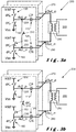
- FIGS 3a and 3b illustrate the switching scheme for a SCPA in accordance with the present disclosure.
- Components previously described with reference to Figure 1 bear the same reference numerals.
- SCPA 200 is shown which is similar to SCPA 100 of Figure 1 but with an additional switch 210, in a switch signal line, connecting capacitors 110, 120 together at nodes 220, 230 as shown.
- the switches 130, 140, 150, 160 operate at RF for the "full amplitude" mode.
- Figure 3b illustrates the switch 210 also being switched at RF with switches 140, 150 being open with no connection to ground, V ss , and switches 130, 160 switching at RF.
- Output 270 from capacitor 110 and output 280 from capacitor 120 are combined at 290 and connect to load node 295.
- the two differential capacitors 110, 120 are switched between the supply voltage, V dd , ground, V ss , and being connected together by switch 210. Effectively, the signal swing at the capacitor is half of the "full amplitude" mode. When none of the cells are in the "off” mode, no power is lost and hence efficiency is preserved down to half of the peak output amplitude.
- node 220 switches between the supply voltage, V dd , ground, V ss .
- node 220 switches between the supply voltage, V dd , and half the supply voltage as switch 140 is open.
- signals applied to node 230 are the inverse or complement of those applied to node 230, switching between ground, V ss , and half the supply voltage, V dd .
- n f is the number of cells in the "full amplitude” mode
- n h is the number of cells in the "half amplitude” mode
- N is the total number of cells.
- n f and n h should be less than or equal to N. This assumes that all cells have equal weight (unary scaling). However, this is not necessarily the case. Binary scaling or a combination of unary and binary scaling is also possible (segmented).
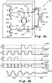
- the switching scheme of the present disclosure can be implemented in two ways using transistors as shown in Figures 5a & 5b and 6a & 6b and as described in more detail below.
- V dd power supply voltage
- V max maximum safe transistor voltage
- the embodiment shown in Figure 5a is used, and when using a power supply voltage, V dd , higher than the maximum safe transistor voltage, V max , but lower than twice the maximum safe transistor voltage, V max , the embodiment of Figure 6a is used.
- the SCPA 400 comprises first and second capacitors 410, 420 where the first capacitor 110 is connected to transistors 430, 440, in a first signal line, which, in turn, are connected to a supply voltage, V dd , and to ground, V ss , respectively.
- Transistors 430, 440 are switched at an applied RF.
- the second capacitor 420 is connected to transistors 450, 460, in a second signal line, which, in turn, are connected to a supply voltage, V dd , and to ground, V ss , respectively.
- Transistors 450, 460 are also switched at the applied RF.
- Input signals to transistors 430 and 460 are such that transistor 430 receives signal B and transistor 460 receives signal B .
- input signals to transistors 440 and 450 are such that transistor 440 receives signal A and transistor 450 receives signal A .
- Differential outputs 470, 480 from the first and second capacitors 410, 420 are combined at 490 and connect to a load node 495.
- Input signals to transistors 450 and 460 are effectively inverted signals of input signals to transistors 440 and 430 respectively.
- An additional transistor arrangement 510 is shown, in a switch signal line, connecting capacitors 410, 420 together at nodes 520, 530.
- the transistor arrangement 510 comprise first and second transistors 540, 550 where input signals to transistors 550, 540 are such that transistor 540 receives input signal C and transistor 550 receives signal C .
- only one of the first and second transistors 540, 550 need be present to implement the switch 510.
- transistors 430, 460, 540, 550 are switched at the RF frequency, thereby generating a square wave with an amplitude of 0.5*V dd at nodes 520 and 530.
- the output amplitude of the "half amplitude" mode is half of the "full amplitude” mode.
- transistors 440, 450, 540 and 550 are off, and, transistors 430 and 460 tie nodes 520 and 530 at V dd and V ss respectively.
- Other options for the "off" mode are possible, where the nodes 520 and 530 are connected to either one of V dd or V ss or connected together.
- Figure 5b shows waveforms A, B and C at inputs to transistors 440, 460, 540, at nodes 520, 530 ( Act_p, Act _ n ), and at load node 495 ( Out ) for all three modes.
- Waveforms 440W, 430W, 540W, 520W, 530W and 495W correspond to respective ones of the inputs to the transistors 440, 430, 540, at the nodes 520, 530, and at load node 495 for all three modes.
- Sections 495a, 495b and 495c of the waveform 495W correspond respectively to "full amplitude" mode, "half amplitude” mode and "off” mode.
- Each cell comprises first and second capacitors 610, 620 connected to respective ones of outputs 670 and 680 which are combined at 690 to provide an output load node 695.
- the first capacitor 610 is in a first signal line and the second capacitor 620 is in a second signal line.
- Transistors 630 and 650 are connected to the higher supply voltage, 2V dd , and transistors 640 and 660 are connected to ground, V ss .
- the bias voltage V dd is connected to transistors 635, 645, 655, 665 as shown.
- Transistor 640 receives input signal A and transistor 660 receives input signal A', with transistor 630 receiving input signal B and transistor 650 input signal B'.
- transistor arrangement 710 comprises transistors 740, 745, 750 and 755 as shown, where input signal to transistor 740 is D with input signal to transistor 750 being D' and, input signal to transistor 745 is C with input signal to transistor 755 being C'.
- V dd exists between transistors 745 and 750 as shown, and it does not need to be supplied externally with a voltage supply or stabilizing circuit. However, this embodiment does not exclude the use of a voltage supply or stabilizing circuit. Although the voltage V dd is the same as the gate for transistors 635, 645, 655, 665, in essence, the gate side and switching side do not need to be connected although they could be.
- transistors 640, 630, 650 and 660 are switched at the applied RF, thereby generating a square wave with an amplitude of 2V dd at nodes 720 and 730.
- Transistors 745, 740, 755 and 750 are controlled such that the connection between nodes 720 and 730 is open.
- transistors 630, 740, 755 and 660 are switched at the RF frequency, thereby generating a square wave with an amplitude of 0.5* 2V dd at nodes 720, 730.
- the output amplitude of the "half amplitude" mode is half of the "full amplitude” mode.
- transistors 745, 740, 755 and 750 are configured such that nodes 720, 730 are statically connected together.
- Other options for the "off" mode are possible, where the nodes 720 and 730 are connected to either V ss or V dd .
Landscapes
- Engineering & Computer Science (AREA)
- Power Engineering (AREA)
- Amplifiers (AREA)
Abstract
Description
- The present disclosure relates to improvements in or relating to switched-capacitor power amplifiers, and is more particularly concerned with improving the efficiency of such amplifiers at back-off.
- Power amplifiers are important building blocks in wireless transmitters. In switched-capacitor class D power amplifiers, for full output power, all cells switch an output capacitor between the supply voltage and the ground at the radio frequency (RF) frequency. Amplitude modulation is performed by disabling some of the cells, and, a disabled cell shorts the capacitor to either the supply voltage or ground. The efficiency of such power amplifiers is a function of the output amplitude. Whilst the efficiency at the peak output power is usually good, it degrades rapidly for lower output amplitudes. This degraded efficiency is caused by the off-cells which attenuate the output signal and consuming a part of its power.
- When a switched-capacitor power amplifier operates at back-off, for example, at around 30% output amplitude (back-off being at any percentage between 0% and 100%), the efficiency is degraded with respect to the peak output power, and, when the output signal has a peak-to-average-power-ratio, the average efficiency is degraded with respect to the peak efficiency. Back-off is the output of a power amplifier when the output is not at its maximum value, but at a lower value than its maximum value. Hence, the output power is reduced with respect to the maximum output power. For signals with a non-constant amplitude, hence, with a large peak-to-average power ratio (PAPR), the power amplifier operates continuously in back-off. This means that, for these signals, the efficiency is also reduced with respect to the efficiency at maximum output power.
- There are existing approaches for improving the efficiency at back-off. In one approach, the supply voltage can be used to modulate efficiently the switched-capacitor power amplifier (SCPA) output amplitude. However, the resulting amplitude range is limited. When the threshold voltage of the transistors is reached, the efficiency drops rapidly. Furthermore, this method has a very non-linear transfer from the supply voltage to output amplitude. In another approach, the use of two power supplies is proposed for improving efficiency at back-off (as described in "A Class-G Switched-Capacitor RF Power Amplifier" by S.M. Yoo et al., IEEE Journal of Solid-State Circuits, Vol. 48, No. 5, pages 1212 to 1224, May 2013). However, such an approach has increased overheads due to the provision of the second power supply and its associated connections.
- In another approach, a Doherty amplifier has an improved efficiency at back-off by adding the outputs of two amplifiers, one for the normal range and one for the peak output amplitude values. However, such amplifiers tend to work only with small frequency ranges and require significant design effort.
- In a further approach, the power amplifiers are stacked for efficiency enhancement at back-off (as described in "A 1.8GHz linear CMOS power amplifier with supply-path switching scheme for WCDMA/LTE applications" by K. Onizuka et al., IEEE International Solid-State Circuits Conference Digest of Technical Papers, San Francisco, CA, 2013, pages 90 to 91). The circuit consists of two power amplifiers arranged in parallel so that their output power is added. For peak output amplitude, both power amplifiers are supplied by the full supply voltage. When the required output amplitude is half of the peak output amplitude, one power amplifier is supplied by maximum supply and half the maximum supply, and, the other power amplifier is supplied with half the maximum supply and ground. In this way, each power amplifier receives half the supply voltage and produces half the output amplitude while maintaining high efficiency.
- An implementation of such an amplifier is described in
US-A-2015/0155832 where a power amplifier comprises first and second amplifier units which are connected to separate power supplies and which connected together to form an intermediate node. A first switching element is provided between a ground terminal of the first amplifier and a power supply terminal of the second amplifier, a second switching element is provided between a ground terminal of the first amplifier and a first reference voltage terminal, and, a third switching element is provided between the power supply terminal of the second amplifier and a second reference voltage terminal. Control logic is used to operate the switches in the connections between the first and second amplifier units and their respective power supply terminals. - Whilst improved efficiency at back-off may be obtained using such an amplifier arrangement, this amplifier arrangement requires a "voltage holding circuit" as well as complex circuitry to implement amplitude modulation with sufficient resolution.
- It is an object of the present disclosure to provide a novel switching scheme for switched-capacitor power amplifiers which improves the efficiency at back-off without loss of peak output power and while only using one power supply voltage.
- In accordance with one aspect of the present disclosure, there is provided a cell for a switched-capacitor power amplifier comprising:
- first and second differential capacitors configured for providing a differential full amplitude output signal therefrom;
- first and second input signal lines configured to be connected to respective ones of the first differential capacitors;
- first and second switches provided in the first input signal line, the first switch being configured for supplying a first voltage supply to the first input signal line and the second switch being configured for supplying a second voltage supply to the first input signal line, the first and second switches being switched at a predetermined radio frequency;
- third and fourth switches provided in the second input signal line, the third switch being configured for supplying the first voltage supply to the second input signal line and the fourth switch being configured for supplying the second voltage supply to the second input signal line, the third and fourth switches being switched at the predetermined radio frequency with the first and fourth switches being switched together and the second and third switches being switched together; and
- a switched signal line between the first and second signal lines, the switched signal line including a further switch which is configured to be switched at the predetermined radio frequency in accordance with the first and fourth switches, the switched signal line providing a differential half amplitude output signal.
- By providing a "half amplitude" mode as well as a "full amplitude" mode in each cell, it is possible to generate an output amplitude which is lower than the maximum output amplitude, without configuring some of the PA cells in the "off" mode and thereby losing efficiency. Moreover, due to the use of the "half amplitude" mode, the efficiency at back-off remains approximately equal to the efficiency at maximum output amplitude, thereby providing efficiency enhancement at each level of output-power back-off, and, the efficiency enhancement is not limited to specific output-power back-off values of the prior art.
- In an embodiment, the further switch comprises first and second further switch elements, the first and second further switch elements being configured to be switched together.
- In another embodiment, the first switch comprises first and second switch elements and second switch comprises third and fourth switch elements, the second switch element and the third switch element being connected to one another and to a third supply voltage, the third supply voltage being lower than the first supply voltage but greater than the second supply voltage.
- Similarly, the third switch comprises fifth and sixth switch elements and fourth switch comprises seventh and eighth switch elements, the sixth switch element and the seventh switch element being connected to one another and to the third supply voltage, the third supply voltage being lower than the first supply voltage but greater than the second supply voltage.
- In a further embodiment, the further switch comprises four switch elements configured as two pairs of switches, and, the switch signal line defines a central node at the third voltage.
- In one embodiment, the second voltage comprises ground.
- In accordance with another aspect of the present disclosure, there is provided a switched-capacitor power amplifier comprising a plurality of cells as described above, wherein the differential output signal from each cell is connected together to form a combined differential output signal.
- In accordance with a further aspect of the present disclosure, there is provided a method of operating a cell for a switched-capacitor power amplifier, the method comprising the steps of:
- connecting first and second differential capacitors in respective first and second input signal lines, the first and second differential capacitors being configured for providing a differential full amplitude output signal therefrom;
- connecting first and second switches in the first signal line;
- supplying first and second voltage supplies to the first input signal line by way of respective ones of the first and second switches;
- switching the first and second switches at a predetermined radio frequency;
- connecting third and fourth switches in the second input signal line;
- supplying the first and second voltage supplies to the second input signal line by way of respective ones of the third and fourth switches;
- switching the third and fourth switches at the predetermined radio frequency, the first and fourth switches being switched together and the second and third switches being switched together;
- connecting a further switch between the first and second signal lines; and
- switching the further switch at the predetermined radio frequency in accordance with the first and fourth switches to provide a differential half amplitude output signal, the second and third switches being in an open condition.
- In accordance with a yet further aspect of the present disclosure, there is provided a method of operating a switched-capacitor power amplifier, the method comprising performing for each cell, the method as described above.
- For a better understanding of the present disclosure, reference will now be made, by way of example, to the accompanying drawings in which:-
-
Figure 1 illustrates a schematic view of a conventional switched-capacitor class-D power amplifier; -
Figure 2 is a graph illustrating typical efficiency of the power amplifier ofFigure 1 ; -
Figures 3a and 3b illustrate schematic views of a switched-capacitor power amplifier in accordance with the present disclosure at "full output amplitude" and "half output amplitude" respectively; -
Figure 4a is a graph illustrating a comparison of a number of cells in the "full amplitude" mode, the "half amplitude" mode and an "off" mode, depending on the desired relative output amplitude; -
Figure 4b is a graph illustrating a comparison of efficiency for a conventional switched-capacitor power amplifier and for a switched-capacitor power amplifier in accordance with the present disclosure; -
Figure 5a illustrates a schematic view of one embodiment of a switched-capacitor power amplifier in accordance with the present disclosure where the supply is less than the maximum safe transistor voltage; -
Figure 5b illustrates the waveforms for the embodiment shown inFigure 5a ; -
Figure 6a illustrates a schematic view of another embodiment of a switched-capacitor power amplifier in accordance with the present disclosure where the supply is between a maximum safe transistor voltage and twice the maximum safe transistor voltage; and -
Figure 6b illustrates the waveforms for the embodiment shown inFigure 6a . - The present disclosure will be described with respect to particular embodiments and with reference to certain drawings but the disclosure is not limited thereto. The drawings described are only schematic and are nonlimiting. In the drawings, the size of some of the elements may be exaggerated and not drawn on scale for illustrative purposes.
-
Figure 1 illustrates a conventional switched-capacitor power amplifier (SCPA) 100 comprising a plurality of cells, each cell comprising differential capacitors, namely, first andsecond capacitors first capacitor 110 is connected, in a first signal line, toswitches Switches second capacitor 120 is connected, in a second signal line, toswitches Switches switches Differential outputs second capacitors load 195. Although only one cell is shown, it will readily be appreciated that similar, if not identical, arrangements are provided in the other cells. - Although Vss is described as being ground, this can be any other suitable voltage which is lower than the supply voltage, Vdd.
- For full power output, all cells switch the first and
second output capacitors - As described above, the efficiency of a SCPA is a function of its output amplitude. A typical efficiency curve as a function of normalized output amplitude is shown in
Figure 2 . As shown, the efficiency at peak output amplitude is good but falls off as output amplitude decreases. - In accordance with the present disclosure, a switching scheme for a SCPA is provided which addresses the issue of reduced efficiency at back-off, that is, at reduced output amplitude. In contrast to conventional SCPAs, the present disclosure provides a SCPA with not only a "full amplitude" mode and an "off" mode but a "half amplitude" mode. Cells are changed to "half amplitude" when a lower output amplitude is required, and, when an even lower output amplitude is required, some of the cells are switched to the "off" mode.
-
Figures 3a and 3b illustrate the switching scheme for a SCPA in accordance with the present disclosure. Components previously described with reference toFigure 1 bear the same reference numerals. - In
Figure 3a ,SCPA 200 is shown which is similar toSCPA 100 ofFigure 1 but with anadditional switch 210, in a switch signal line, connectingcapacitors nodes Figure 1 , theswitches -
Figure 3b illustrates theswitch 210 also being switched at RF withswitches Output 270 fromcapacitor 110 andoutput 280 fromcapacitor 120 are combined at 290 and connect to loadnode 295. - In this way, the two
differential capacitors switch 210. Effectively, the signal swing at the capacitor is half of the "full amplitude" mode. When none of the cells are in the "off" mode, no power is lost and hence efficiency is preserved down to half of the peak output amplitude. - In "full amplitude" mode (as shown in
Figure 3a ),node 220 switches between the supply voltage, Vdd , ground, Vss . Signals applied tonode 230 are the inverse or complement to those applied tonode 220. If all cells are in this mode, the output power, Pout, is:
load node 295 assuming that Vss = 0. - When all cells are in the "half amplitude" mode (as shown in
figure 3b ),node 220 switches between the supply voltage, Vdd , and half the supply voltage asswitch 140 is open. Similarly, signals applied tonode 230 are the inverse or complement of those applied tonode 230, switching between ground, Vss , and half the supply voltage, Vdd. The output power is:
- In general, the output power of the SCPA in accordance with the present disclosure is:

- The sum of nf and nh should be less than or equal to N. This assumes that all cells have equal weight (unary scaling). However, this is not necessarily the case. Binary scaling or a combination of unary and binary scaling is also possible (segmented).
- For optimal efficiency, a specific sequence of enabling the different modes is required. However, other sequences may be used for enabling the different modes. The number of "full amplitude", "half amplitude" and "off" cells is dependent on the output amplitude as shown in
Figure 4a .Line 300 refers to the "off" cells;line 310 refers to the "half amplitude" cells; andline 320 refers to the "full amplitude" cells. The resulting efficiency curve is shown isFigure 4b whereline 350 refers to the efficiency of a conventional SCPA as shown inFigure 2 , and,line 360 refers to the efficiency of a SCPA in accordance with the present disclosure. As shown, the efficiency of the SCPA in accordance with the present disclosure is better at lower normalized output amplitudes than conventional SCPA, for example, as shown inFigure 1 . - The switching scheme of the present disclosure can be implemented in two ways using transistors as shown in
Figures 5a & 5b and6a & 6b and as described in more detail below. When using a power supply voltage, Vdd , lower than the maximum safe transistor voltage, Vmax , the embodiment shown inFigure 5a is used, and when using a power supply voltage, Vdd , higher than the maximum safe transistor voltage, Vmax, but lower than twice the maximum safe transistor voltage, Vmax , the embodiment ofFigure 6a is used. - Referring initially to
Figure 5a , aSCPA 400 in accordance with the present disclosure is shown where the switches ofFigures 3a and 3b are implemented by transistors. TheSCPA 400 comprises first andsecond capacitors first capacitor 110 is connected totransistors Transistors second capacitor 420 is connected totransistors Transistors - Input signals to
transistors transistor 430 receives signal B andtransistor 460 receives signalB . Similarly, input signals totransistors transistor 440 receives signal A andtransistor 450 receives signalA . -
Differential outputs second capacitors load node 495. Input signals totransistors transistors - An
additional transistor arrangement 510 is shown, in a switch signal line, connectingcapacitors nodes transistor arrangement 510 comprise first andsecond transistors transistors transistor 540 receives input signal C andtransistor 550 receives signalC . - In a non-illustrated embodiment, only one of the first and
second transistors switch 510. - As before, although only one cell is shown, it will readily be appreciated that similar if not identical arrangements are provided in the other cells, and, that the output from each cell is connected to form
differential outputs - In the "full amplitude" mode,
transistors node 520 and at node 530 (assuming Vss = 0). - In the "half amplitude" mode,
transistors nodes - In the "off" mode,
transistors transistors tie nodes nodes -
Figure 5b shows waveforms A, B and C at inputs totransistors nodes 520, 530 (Act_p, Act_n), and at load node 495 (Out) for all three modes.Waveforms transistors nodes load node 495 for all three modes.Sections waveform 495W correspond respectively to "full amplitude" mode, "half amplitude" mode and "off" mode. It will readily be understood that as the input signals totransistors transistors transistors transistors - Turning now to
Figure 6a , aSCPA 600 used when using a power supply voltage Vdd higher than the maximum transistor voltage Vmax but lower than twice the maximum transistor voltage 2Vmax is shown. Each cell comprises first andsecond capacitors outputs output load node 695. As before, thefirst capacitor 610 is in a first signal line and thesecond capacitor 620 is in a second signal line. - In this embodiment, there are still only two supply voltages, namely, twice the supply voltage, 2Vdd compared to
Figure 5a , and ground, Vss as before.Transistors transistors transistors Transistor 640 receives input signal A andtransistor 660 receives input signal A', withtransistor 630 receiving input signal B andtransistor 650 input signal B'. -
Nodes transistor arrangement 710 in a switch signal line. In this embodiment,transistor arrangement 710 comprisestransistors transistor 740 is D with input signal totransistor 750 being D' and, input signal totransistor 745 is C with input signal totransistor 755 being C'. In this embodiment, Vdd exists betweentransistors transistors - In the "full amplitude" mode,
transistors nodes Transistors nodes - In the "half amplitude" mode,
transistors nodes - In the "off" mode,
transistors nodes nodes - The corresponding
waveforms 640W (A), 660W (A'), 630W (B), 650W (B'), 745W (C), 755W (C'), 740W (D), 750W (D') of input signals totransistors nodes 720, 730 (Act_p, Act_n) and at load node 795 (Out) are shown inFigure 6b , for all three modes. Sections 795a, 795b and 795c respectively illustrate the "full amplitude", "half amplitude" and "off" modes. - Advantages of the method in accordance with the present disclosure include:
- Power amplifier efficiency improved in back-off;
- Power amplifier efficiency improved for signals with high PAPR;
- Efficiency improvement is independent of frequency or bandwidth; and
- No additional power supplies are required to generate the "half amplitude" mode.
- Although specific implementations for switching the cells of the SCPA in accordance with the present disclosure, it will readily be appreciated that other implementations for achieving the same switching regime may be possible.
Claims (9)
- A cell for a switched-capacitor power amplifier comprising:first and second differential capacitors configured for providing a differential full amplitude output signal therefrom;first and second input signal lines configured to be connected to respective ones of the first differential capacitors;first and second switches provided in the first input signal line, the first switch being configured for supplying a first voltage supply to the first input signal line and the second switch being configured for supplying a second voltage supply to the first input signal line, the first and second switches being switched at a predetermined radio frequency;third and fourth switches provided in the second input signal line, the third switch being configured for supplying the first voltage supply to the second input signal line and the fourth switch being configured for supplying the second voltage supply to the second input signal line, the third and fourth switches being switched at the predetermined radio frequency with the first and fourth switches being switched together and the second and third switches being switched together; anda switched signal line between the first and second signal lines, the switched signal line including a further switch which is configured to be switched at the predetermined radio frequency in accordance with the first and fourth switches, the switched signal line providing a differential half amplitude output signal.
- A cell according to claim 1, wherein the further switch comprises first and second further switch elements, the first and second further switch elements being configured to be switched together.
- A cell according to claim 1, wherein the first switch comprises first and second switch elements and second switch comprises third and fourth switch elements, the second switch element and the third switch element being connected to one another and to a third supply voltage, the third supply voltage being lower than the first supply voltage but greater than the second supply voltage.
- A cell according to claim 3, wherein the third switch comprises fifth and sixth switch elements and fourth switch comprises seventh and eighth switch elements, the sixth switch element and the seventh switch element being connected to one another and to the third supply voltage, the third supply voltage being lower than the first supply voltage but greater than the second supply voltage.
- A cell according to claim 4, wherein the further switch comprises four switch elements configured as two pairs of switches, and, the switch signal line defines a central node at the third voltage.
- A cell according to any one of claims 1 to 5, wherein the second voltage comprises ground.
- A switched-capacitor power amplifier comprising a plurality of cells according to any one of claims 1 to 6, wherein the differential output signal from each cell is connected together to form a combined output.
- A method of operating a cell for a switched-capacitor power amplifier the method comprising the steps of:connecting first and second differential capacitors in respective first and second input signal lines, the first and second differential capacitors being configured for providing a differential full amplitude output signal therefrom;connecting first and second switches in the first signal line;supplying first and second voltage supplies to the first input signal line by way of respective ones of the first and second switches;switching the first and second switches at a predetermined radio frequency;connecting third and fourth switches in the second input signal line;supplying the first and second voltage supplies to the second input signal line by way of respective ones of the third and fourth switches;switching the third and fourth switches at the predetermined radio frequency, the first and fourth switches being switched together and the second and third switches being switched together;connecting a further switch between the first and second signal lines; andswitching the further switch at the predetermined radio frequency in accordance with the first and fourth switches to provide a differential half amplitude output signal, the second and third switches being in an open condition.
- A method of operating a switched-capacitor power amplifier, the method comprising performing for each cell, the method according to claim 8.
Priority Applications (3)
| Application Number | Priority Date | Filing Date | Title |
|---|---|---|---|
| EP17208089.7A EP3499718B1 (en) | 2017-12-18 | 2017-12-18 | Improvements in or relating to switched-capacitor power amplifiers |
| JP2018206811A JP7064427B2 (en) | 2017-12-18 | 2018-11-01 | Switched Capacitor Power Amplifier Improvements or Related |
| US16/222,340 US10862439B2 (en) | 2017-12-18 | 2018-12-17 | Switched-capacitor power amplifiers |
Applications Claiming Priority (1)
| Application Number | Priority Date | Filing Date | Title |
|---|---|---|---|
| EP17208089.7A EP3499718B1 (en) | 2017-12-18 | 2017-12-18 | Improvements in or relating to switched-capacitor power amplifiers |
Publications (2)
| Publication Number | Publication Date |
|---|---|
| EP3499718A1 true EP3499718A1 (en) | 2019-06-19 |
| EP3499718B1 EP3499718B1 (en) | 2021-07-07 |
Family
ID=60673817
Family Applications (1)
| Application Number | Title | Priority Date | Filing Date |
|---|---|---|---|
| EP17208089.7A Active EP3499718B1 (en) | 2017-12-18 | 2017-12-18 | Improvements in or relating to switched-capacitor power amplifiers |
Country Status (3)
| Country | Link |
|---|---|
| US (1) | US10862439B2 (en) |
| EP (1) | EP3499718B1 (en) |
| JP (1) | JP7064427B2 (en) |
Families Citing this family (2)
| Publication number | Priority date | Publication date | Assignee | Title |
|---|---|---|---|---|
| US10862425B2 (en) * | 2019-04-25 | 2020-12-08 | Shenzhen GOODIX Technology Co., Ltd. | Differential switchable capacitors for radiofrequency power amplifiers |
| US12255653B2 (en) * | 2021-06-24 | 2025-03-18 | Intel Corporation | Methods and devices for digital clock multiplication of a clock to generate a high frequency output |
Citations (4)
| Publication number | Priority date | Publication date | Assignee | Title |
|---|---|---|---|---|
| US8547177B1 (en) * | 2010-05-12 | 2013-10-01 | University Of Washington Through Its Center For Commercialization | All-digital switched-capacitor radio frequency power amplification |
| US20140077876A1 (en) * | 2012-09-17 | 2014-03-20 | Samsung Electronics Co., Ltd. | Wireless communication system with power amplifier mechanism and method of operation thereof |
| US20150155832A1 (en) | 2012-08-13 | 2015-06-04 | Kabushiki Kaisha Toshiba | Power amplifier and transmitter |
| US20160336909A1 (en) * | 2015-05-13 | 2016-11-17 | Qualcomm Incorporated | Switched capacitor power amplifier circuits and methods |
Family Cites Families (5)
| Publication number | Priority date | Publication date | Assignee | Title |
|---|---|---|---|---|
| DE602004006974T2 (en) | 2003-03-10 | 2008-02-28 | Koninklijke Philips Electronics N.V. | THREE STATE CLASS-D AMPLIFIER |
| EP2274829B1 (en) * | 2008-05-05 | 2012-09-05 | Nxp B.V. | Efficient linear linc power amplifier |
| CN106027014B (en) * | 2012-05-11 | 2019-10-01 | 意法半导体研发(深圳)有限公司 | Current slope control method and device for power driver circuit application |
| JP6486938B2 (en) | 2013-09-10 | 2019-03-20 | エフィシエント パワー コンヴァーション コーポレーション | High efficiency voltage mode class D topology |
| US9520906B2 (en) | 2014-06-25 | 2016-12-13 | Qualcomm Incorporated | Switched capacitor transmitter circuits and methods |
-
2017
- 2017-12-18 EP EP17208089.7A patent/EP3499718B1/en active Active
-
2018
- 2018-11-01 JP JP2018206811A patent/JP7064427B2/en active Active
- 2018-12-17 US US16/222,340 patent/US10862439B2/en active Active
Patent Citations (4)
| Publication number | Priority date | Publication date | Assignee | Title |
|---|---|---|---|---|
| US8547177B1 (en) * | 2010-05-12 | 2013-10-01 | University Of Washington Through Its Center For Commercialization | All-digital switched-capacitor radio frequency power amplification |
| US20150155832A1 (en) | 2012-08-13 | 2015-06-04 | Kabushiki Kaisha Toshiba | Power amplifier and transmitter |
| US20140077876A1 (en) * | 2012-09-17 | 2014-03-20 | Samsung Electronics Co., Ltd. | Wireless communication system with power amplifier mechanism and method of operation thereof |
| US20160336909A1 (en) * | 2015-05-13 | 2016-11-17 | Qualcomm Incorporated | Switched capacitor power amplifier circuits and methods |
Non-Patent Citations (3)
| Title |
|---|
| K. ONIZUKA ET AL.: "A 1.8GHz linear CMOS power amplifier with supply-path switching scheme for WCDMA/LTE applications", IEEE INTERNATIONAL SOLID-STATE CIRCUITS CONFERENCE DIGEST OF TECHNICAL PAPERS, 2013, pages 90 - 91, XP032350487, DOI: doi:10.1109/ISSCC.2013.6487650 |
| S.M. YOO ET AL.: "A Class-G Switched-Capacitor RF Power Amplifier", IEEE JOURNAL OF SOLID-STATE CIRCUITS, vol. 48, no. 5, May 2013 (2013-05-01), pages 1212 - 1224 |
| SANG-MIN YOO ET AL: "A class-G dual-supply switched-capacitor power amplifier in 65nm CMOS", 2012 IEEE RADIO FREQUENCY INTEGRATED CIRCUITS SYMPOSIUM (RFIC); ?MONTREAL, QC, CANADA; 17-19 JUNE 2012, IEEE, PISCATAWAY, NJ, USA, 17 June 2012 (2012-06-17), pages 233 - 236, XP032203344, ISBN: 978-1-4673-0413-9, DOI: 10.1109/RFIC.2012.6242271 * |
Also Published As
| Publication number | Publication date |
|---|---|
| US20190190465A1 (en) | 2019-06-20 |
| EP3499718B1 (en) | 2021-07-07 |
| JP2019110523A (en) | 2019-07-04 |
| US10862439B2 (en) | 2020-12-08 |
| JP7064427B2 (en) | 2022-05-10 |
Similar Documents
| Publication | Publication Date | Title |
|---|---|---|
| US11171616B2 (en) | Multi-branch outphasing system and method | |
| EP2806557B1 (en) | Doherty amplifier | |
| US9385669B2 (en) | Class-E outphasing power amplifier with efficiency and output power enhancement circuits and method | |
| US9374041B2 (en) | Doherty power amplification apparatus and method | |
| EP1040567B1 (en) | Power amplification apparatus and method therefor | |
| US8115546B2 (en) | Apparatus and method for maximizing performance of peaking amplifier in doherty amplifier | |
| US20100073084A1 (en) | Systems and methods for a level-shifting high-efficiency linc amplifier using dynamic power supply | |
| EP2858236A1 (en) | Power amplifiers with signal conditioning | |
| KR101841670B1 (en) | Outphasing power amplifier signal splitter using next stage input impedance and multiple biasing | |
| KR101119374B1 (en) | Asymmetrical Power Divider | |
| CN102710225A (en) | Multilevel class-d amplifier | |
| CN109417394B (en) | Envelope Modulator, Envelope Tracking Power Amplifier and Communication Equipment | |
| EP3499718B1 (en) | Improvements in or relating to switched-capacitor power amplifiers | |
| US20250070723A1 (en) | Amplifier circuit and method of generating an amplified signal | |
| JP2014039109A (en) | Power amplifier and transmitter | |
| US11356069B2 (en) | Digital power amplifier | |
| WO2016207582A1 (en) | Amplifier circuitry and method for amplifying a signal using said amplifier circuitry | |
| US20220271716A1 (en) | Power amplifier combiner apparatus and power amplifier circuit | |
| CN104734652B (en) | A kind of rail-to-rail operational amplifier | |
| US10536118B2 (en) | Circuit and a method for operating a circuit | |
| Roberts | Understanding the 3 level Doherty | |
| Bieg et al. | A CMOS switching mode amplifier with 3 V output swing for continuous-wave frequencies up to 4 GHz | |
| Bachi et al. | New analytical boundary condition for optimized outphasing PA design | |
| CN218633891U (en) | Function waveform modulation circuit | |
| JP5554842B2 (en) | High frequency amplifier |
Legal Events
| Date | Code | Title | Description |
|---|---|---|---|
| PUAI | Public reference made under article 153(3) epc to a published international application that has entered the european phase |
Free format text: ORIGINAL CODE: 0009012 |
|
| STAA | Information on the status of an ep patent application or granted ep patent |
Free format text: STATUS: THE APPLICATION HAS BEEN PUBLISHED |
|
| AK | Designated contracting states |
Kind code of ref document: A1 Designated state(s): AL AT BE BG CH CY CZ DE DK EE ES FI FR GB GR HR HU IE IS IT LI LT LU LV MC MK MT NL NO PL PT RO RS SE SI SK SM TR |
|
| AX | Request for extension of the european patent |
Extension state: BA ME |
|
| STAA | Information on the status of an ep patent application or granted ep patent |
Free format text: STATUS: REQUEST FOR EXAMINATION WAS MADE |
|
| 17P | Request for examination filed |
Effective date: 20191118 |
|
| RBV | Designated contracting states (corrected) |
Designated state(s): AL AT BE BG CH CY CZ DE DK EE ES FI FR GB GR HR HU IE IS IT LI LT LU LV MC MK MT NL NO PL PT RO RS SE SI SK SM TR |
|
| STAA | Information on the status of an ep patent application or granted ep patent |
Free format text: STATUS: EXAMINATION IS IN PROGRESS |
|
| 17Q | First examination report despatched |
Effective date: 20210218 |
|
| GRAP | Despatch of communication of intention to grant a patent |
Free format text: ORIGINAL CODE: EPIDOSNIGR1 |
|
| STAA | Information on the status of an ep patent application or granted ep patent |
Free format text: STATUS: GRANT OF PATENT IS INTENDED |
|
| INTG | Intention to grant announced |
Effective date: 20210419 |
|
| GRAS | Grant fee paid |
Free format text: ORIGINAL CODE: EPIDOSNIGR3 |
|
| GRAA | (expected) grant |
Free format text: ORIGINAL CODE: 0009210 |
|
| STAA | Information on the status of an ep patent application or granted ep patent |
Free format text: STATUS: THE PATENT HAS BEEN GRANTED |
|
| AK | Designated contracting states |
Kind code of ref document: B1 Designated state(s): AL AT BE BG CH CY CZ DE DK EE ES FI FR GB GR HR HU IE IS IT LI LT LU LV MC MK MT NL NO PL PT RO RS SE SI SK SM TR |
|
| REG | Reference to a national code |
Ref country code: GB Ref legal event code: FG4D |
|
| REG | Reference to a national code |
Ref country code: AT Ref legal event code: REF Ref document number: 1409560 Country of ref document: AT Kind code of ref document: T Effective date: 20210715 |
|
| REG | Reference to a national code |
Ref country code: DE Ref legal event code: R096 Ref document number: 602017041567 Country of ref document: DE |
|
| REG | Reference to a national code |
Ref country code: IE Ref legal event code: FG4D |
|
| REG | Reference to a national code |
Ref country code: LT Ref legal event code: MG9D |
|
| REG | Reference to a national code |
Ref country code: NL Ref legal event code: MP Effective date: 20210707 |
|
| REG | Reference to a national code |
Ref country code: AT Ref legal event code: MK05 Ref document number: 1409560 Country of ref document: AT Kind code of ref document: T Effective date: 20210707 |
|
| PG25 | Lapsed in a contracting state [announced via postgrant information from national office to epo] |
Ref country code: AT Free format text: LAPSE BECAUSE OF FAILURE TO SUBMIT A TRANSLATION OF THE DESCRIPTION OR TO PAY THE FEE WITHIN THE PRESCRIBED TIME-LIMIT Effective date: 20210707 Ref country code: BG Free format text: LAPSE BECAUSE OF FAILURE TO SUBMIT A TRANSLATION OF THE DESCRIPTION OR TO PAY THE FEE WITHIN THE PRESCRIBED TIME-LIMIT Effective date: 20211007 Ref country code: LT Free format text: LAPSE BECAUSE OF FAILURE TO SUBMIT A TRANSLATION OF THE DESCRIPTION OR TO PAY THE FEE WITHIN THE PRESCRIBED TIME-LIMIT Effective date: 20210707 Ref country code: NL Free format text: LAPSE BECAUSE OF FAILURE TO SUBMIT A TRANSLATION OF THE DESCRIPTION OR TO PAY THE FEE WITHIN THE PRESCRIBED TIME-LIMIT Effective date: 20210707 Ref country code: PT Free format text: LAPSE BECAUSE OF FAILURE TO SUBMIT A TRANSLATION OF THE DESCRIPTION OR TO PAY THE FEE WITHIN THE PRESCRIBED TIME-LIMIT Effective date: 20211108 Ref country code: NO Free format text: LAPSE BECAUSE OF FAILURE TO SUBMIT A TRANSLATION OF THE DESCRIPTION OR TO PAY THE FEE WITHIN THE PRESCRIBED TIME-LIMIT Effective date: 20211007 Ref country code: ES Free format text: LAPSE BECAUSE OF FAILURE TO SUBMIT A TRANSLATION OF THE DESCRIPTION OR TO PAY THE FEE WITHIN THE PRESCRIBED TIME-LIMIT Effective date: 20210707 Ref country code: FI Free format text: LAPSE BECAUSE OF FAILURE TO SUBMIT A TRANSLATION OF THE DESCRIPTION OR TO PAY THE FEE WITHIN THE PRESCRIBED TIME-LIMIT Effective date: 20210707 Ref country code: SE Free format text: LAPSE BECAUSE OF FAILURE TO SUBMIT A TRANSLATION OF THE DESCRIPTION OR TO PAY THE FEE WITHIN THE PRESCRIBED TIME-LIMIT Effective date: 20210707 Ref country code: RS Free format text: LAPSE BECAUSE OF FAILURE TO SUBMIT A TRANSLATION OF THE DESCRIPTION OR TO PAY THE FEE WITHIN THE PRESCRIBED TIME-LIMIT Effective date: 20210707 Ref country code: HR Free format text: LAPSE BECAUSE OF FAILURE TO SUBMIT A TRANSLATION OF THE DESCRIPTION OR TO PAY THE FEE WITHIN THE PRESCRIBED TIME-LIMIT Effective date: 20210707 |
|
| PG25 | Lapsed in a contracting state [announced via postgrant information from national office to epo] |
Ref country code: PL Free format text: LAPSE BECAUSE OF FAILURE TO SUBMIT A TRANSLATION OF THE DESCRIPTION OR TO PAY THE FEE WITHIN THE PRESCRIBED TIME-LIMIT Effective date: 20210707 Ref country code: LV Free format text: LAPSE BECAUSE OF FAILURE TO SUBMIT A TRANSLATION OF THE DESCRIPTION OR TO PAY THE FEE WITHIN THE PRESCRIBED TIME-LIMIT Effective date: 20210707 Ref country code: GR Free format text: LAPSE BECAUSE OF FAILURE TO SUBMIT A TRANSLATION OF THE DESCRIPTION OR TO PAY THE FEE WITHIN THE PRESCRIBED TIME-LIMIT Effective date: 20211008 |
|
| REG | Reference to a national code |
Ref country code: DE Ref legal event code: R097 Ref document number: 602017041567 Country of ref document: DE |
|
| PG25 | Lapsed in a contracting state [announced via postgrant information from national office to epo] |
Ref country code: DK Free format text: LAPSE BECAUSE OF FAILURE TO SUBMIT A TRANSLATION OF THE DESCRIPTION OR TO PAY THE FEE WITHIN THE PRESCRIBED TIME-LIMIT Effective date: 20210707 |
|
| PLBE | No opposition filed within time limit |
Free format text: ORIGINAL CODE: 0009261 |
|
| STAA | Information on the status of an ep patent application or granted ep patent |
Free format text: STATUS: NO OPPOSITION FILED WITHIN TIME LIMIT |
|
| PG25 | Lapsed in a contracting state [announced via postgrant information from national office to epo] |
Ref country code: SM Free format text: LAPSE BECAUSE OF FAILURE TO SUBMIT A TRANSLATION OF THE DESCRIPTION OR TO PAY THE FEE WITHIN THE PRESCRIBED TIME-LIMIT Effective date: 20210707 Ref country code: SK Free format text: LAPSE BECAUSE OF FAILURE TO SUBMIT A TRANSLATION OF THE DESCRIPTION OR TO PAY THE FEE WITHIN THE PRESCRIBED TIME-LIMIT Effective date: 20210707 Ref country code: RO Free format text: LAPSE BECAUSE OF FAILURE TO SUBMIT A TRANSLATION OF THE DESCRIPTION OR TO PAY THE FEE WITHIN THE PRESCRIBED TIME-LIMIT Effective date: 20210707 Ref country code: EE Free format text: LAPSE BECAUSE OF FAILURE TO SUBMIT A TRANSLATION OF THE DESCRIPTION OR TO PAY THE FEE WITHIN THE PRESCRIBED TIME-LIMIT Effective date: 20210707 Ref country code: CZ Free format text: LAPSE BECAUSE OF FAILURE TO SUBMIT A TRANSLATION OF THE DESCRIPTION OR TO PAY THE FEE WITHIN THE PRESCRIBED TIME-LIMIT Effective date: 20210707 Ref country code: AL Free format text: LAPSE BECAUSE OF FAILURE TO SUBMIT A TRANSLATION OF THE DESCRIPTION OR TO PAY THE FEE WITHIN THE PRESCRIBED TIME-LIMIT Effective date: 20210707 |
|
| 26N | No opposition filed |
Effective date: 20220408 |
|
| PG25 | Lapsed in a contracting state [announced via postgrant information from national office to epo] |
Ref country code: MC Free format text: LAPSE BECAUSE OF FAILURE TO SUBMIT A TRANSLATION OF THE DESCRIPTION OR TO PAY THE FEE WITHIN THE PRESCRIBED TIME-LIMIT Effective date: 20210707 Ref country code: IT Free format text: LAPSE BECAUSE OF FAILURE TO SUBMIT A TRANSLATION OF THE DESCRIPTION OR TO PAY THE FEE WITHIN THE PRESCRIBED TIME-LIMIT Effective date: 20210707 |
|
| REG | Reference to a national code |
Ref country code: CH Ref legal event code: PL |
|
| GBPC | Gb: european patent ceased through non-payment of renewal fee |
Effective date: 20211218 |
|
| REG | Reference to a national code |
Ref country code: BE Ref legal event code: MM Effective date: 20211231 |
|
| PG25 | Lapsed in a contracting state [announced via postgrant information from national office to epo] |
Ref country code: LU Free format text: LAPSE BECAUSE OF NON-PAYMENT OF DUE FEES Effective date: 20211218 Ref country code: IE Free format text: LAPSE BECAUSE OF NON-PAYMENT OF DUE FEES Effective date: 20211218 Ref country code: GB Free format text: LAPSE BECAUSE OF NON-PAYMENT OF DUE FEES Effective date: 20211218 |
|
| PG25 | Lapsed in a contracting state [announced via postgrant information from national office to epo] |
Ref country code: FR Free format text: LAPSE BECAUSE OF NON-PAYMENT OF DUE FEES Effective date: 20211231 Ref country code: BE Free format text: LAPSE BECAUSE OF NON-PAYMENT OF DUE FEES Effective date: 20211231 |
|
| PG25 | Lapsed in a contracting state [announced via postgrant information from national office to epo] |
Ref country code: LI Free format text: LAPSE BECAUSE OF NON-PAYMENT OF DUE FEES Effective date: 20211231 Ref country code: CH Free format text: LAPSE BECAUSE OF NON-PAYMENT OF DUE FEES Effective date: 20211231 |
|
| P01 | Opt-out of the competence of the unified patent court (upc) registered |
Effective date: 20230513 |
|
| PG25 | Lapsed in a contracting state [announced via postgrant information from national office to epo] |
Ref country code: CY Free format text: LAPSE BECAUSE OF FAILURE TO SUBMIT A TRANSLATION OF THE DESCRIPTION OR TO PAY THE FEE WITHIN THE PRESCRIBED TIME-LIMIT Effective date: 20210707 |
|
| PG25 | Lapsed in a contracting state [announced via postgrant information from national office to epo] |
Ref country code: HU Free format text: LAPSE BECAUSE OF FAILURE TO SUBMIT A TRANSLATION OF THE DESCRIPTION OR TO PAY THE FEE WITHIN THE PRESCRIBED TIME-LIMIT; INVALID AB INITIO Effective date: 20171218 |
|
| PG25 | Lapsed in a contracting state [announced via postgrant information from national office to epo] |
Ref country code: MK Free format text: LAPSE BECAUSE OF FAILURE TO SUBMIT A TRANSLATION OF THE DESCRIPTION OR TO PAY THE FEE WITHIN THE PRESCRIBED TIME-LIMIT Effective date: 20210707 |
|
| PG25 | Lapsed in a contracting state [announced via postgrant information from national office to epo] |
Ref country code: TR Free format text: LAPSE BECAUSE OF FAILURE TO SUBMIT A TRANSLATION OF THE DESCRIPTION OR TO PAY THE FEE WITHIN THE PRESCRIBED TIME-LIMIT Effective date: 20210707 |
|
| PG25 | Lapsed in a contracting state [announced via postgrant information from national office to epo] |
Ref country code: MT Free format text: LAPSE BECAUSE OF FAILURE TO SUBMIT A TRANSLATION OF THE DESCRIPTION OR TO PAY THE FEE WITHIN THE PRESCRIBED TIME-LIMIT Effective date: 20210707 |
|
| PGFP | Annual fee paid to national office [announced via postgrant information from national office to epo] |
Ref country code: DE Payment date: 20251126 Year of fee payment: 9 |