EP3499702A1 - Hold-up capacitor charging using fly-back power supply - Google Patents
Hold-up capacitor charging using fly-back power supply Download PDFInfo
- Publication number
- EP3499702A1 EP3499702A1 EP18211910.7A EP18211910A EP3499702A1 EP 3499702 A1 EP3499702 A1 EP 3499702A1 EP 18211910 A EP18211910 A EP 18211910A EP 3499702 A1 EP3499702 A1 EP 3499702A1
- Authority
- EP
- European Patent Office
- Prior art keywords
- voltage
- hold
- capacitor
- voltage source
- switch
- Prior art date
- Legal status (The legal status is an assumption and is not a legal conclusion. Google has not performed a legal analysis and makes no representation as to the accuracy of the status listed.)
- Granted
Links
Images



Classifications
-
- H—ELECTRICITY
- H02—GENERATION; CONVERSION OR DISTRIBUTION OF ELECTRIC POWER
- H02J—ELECTRIC POWER NETWORKS; CIRCUIT ARRANGEMENTS OR SYSTEMS FOR SUPPLYING OR DISTRIBUTING ELECTRIC POWER; SYSTEMS FOR STORING ELECTRIC ENERGY
- H02J7/00—Circuit arrangements for charging or discharging batteries or for supplying loads from batteries
-
- H—ELECTRICITY
- H02—GENERATION; CONVERSION OR DISTRIBUTION OF ELECTRIC POWER
- H02M—APPARATUS FOR CONVERSION BETWEEN AC AND AC, BETWEEN AC AND DC, OR BETWEEN DC AND DC, AND FOR USE WITH MAINS OR SIMILAR POWER SUPPLY SYSTEMS; CONVERSION OF DC OR AC INPUT POWER INTO SURGE OUTPUT POWER; CONTROL OR REGULATION THEREOF
- H02M3/00—Conversion of DC power input into DC power output
- H02M3/02—Conversion of DC power input into DC power output without intermediate conversion into AC
- H02M3/04—Conversion of DC power input into DC power output without intermediate conversion into AC by static converters
- H02M3/06—Conversion of DC power input into DC power output without intermediate conversion into AC by static converters using resistors or capacitors, e.g. potential divider
- H02M3/07—Conversion of DC power input into DC power output without intermediate conversion into AC by static converters using resistors or capacitors, e.g. potential divider using capacitors charged and discharged alternately by semiconductor devices with control electrode, e.g. charge pumps
- H02M3/073—Charge pumps of the Schenkel-type
-
- H—ELECTRICITY
- H02—GENERATION; CONVERSION OR DISTRIBUTION OF ELECTRIC POWER
- H02M—APPARATUS FOR CONVERSION BETWEEN AC AND AC, BETWEEN AC AND DC, OR BETWEEN DC AND DC, AND FOR USE WITH MAINS OR SIMILAR POWER SUPPLY SYSTEMS; CONVERSION OF DC OR AC INPUT POWER INTO SURGE OUTPUT POWER; CONTROL OR REGULATION THEREOF
- H02M3/00—Conversion of DC power input into DC power output
- H02M3/22—Conversion of DC power input into DC power output with intermediate conversion into AC
- H02M3/24—Conversion of DC power input into DC power output with intermediate conversion into AC by static converters
- H02M3/28—Conversion of DC power input into DC power output with intermediate conversion into AC by static converters using discharge tubes with control electrode or semiconductor devices with control electrode to produce the intermediate AC
- H02M3/325—Conversion of DC power input into DC power output with intermediate conversion into AC by static converters using discharge tubes with control electrode or semiconductor devices with control electrode to produce the intermediate AC using devices of a triode or a transistor type requiring continuous application of a control signal
- H02M3/335—Conversion of DC power input into DC power output with intermediate conversion into AC by static converters using discharge tubes with control electrode or semiconductor devices with control electrode to produce the intermediate AC using devices of a triode or a transistor type requiring continuous application of a control signal using semiconductor devices only
-
- H—ELECTRICITY
- H02—GENERATION; CONVERSION OR DISTRIBUTION OF ELECTRIC POWER
- H02M—APPARATUS FOR CONVERSION BETWEEN AC AND AC, BETWEEN AC AND DC, OR BETWEEN DC AND DC, AND FOR USE WITH MAINS OR SIMILAR POWER SUPPLY SYSTEMS; CONVERSION OF DC OR AC INPUT POWER INTO SURGE OUTPUT POWER; CONTROL OR REGULATION THEREOF
- H02M3/00—Conversion of DC power input into DC power output
- H02M3/22—Conversion of DC power input into DC power output with intermediate conversion into AC
- H02M3/24—Conversion of DC power input into DC power output with intermediate conversion into AC by static converters
- H02M3/28—Conversion of DC power input into DC power output with intermediate conversion into AC by static converters using discharge tubes with control electrode or semiconductor devices with control electrode to produce the intermediate AC
- H02M3/325—Conversion of DC power input into DC power output with intermediate conversion into AC by static converters using discharge tubes with control electrode or semiconductor devices with control electrode to produce the intermediate AC using devices of a triode or a transistor type requiring continuous application of a control signal
- H02M3/335—Conversion of DC power input into DC power output with intermediate conversion into AC by static converters using discharge tubes with control electrode or semiconductor devices with control electrode to produce the intermediate AC using devices of a triode or a transistor type requiring continuous application of a control signal using semiconductor devices only
- H02M3/33507—Conversion of DC power input into DC power output with intermediate conversion into AC by static converters using discharge tubes with control electrode or semiconductor devices with control electrode to produce the intermediate AC using devices of a triode or a transistor type requiring continuous application of a control signal using semiconductor devices only with automatic control of the output voltage or current, e.g. flyback converters
-
- H—ELECTRICITY
- H02—GENERATION; CONVERSION OR DISTRIBUTION OF ELECTRIC POWER
- H02J—ELECTRIC POWER NETWORKS; CIRCUIT ARRANGEMENTS OR SYSTEMS FOR SUPPLYING OR DISTRIBUTING ELECTRIC POWER; SYSTEMS FOR STORING ELECTRIC ENERGY
- H02J2207/00—Details of circuit arrangements for charging or discharging batteries or supplying loads from batteries
- H02J2207/20—Charging or discharging characterised by the power electronics converter
-
- H—ELECTRICITY
- H02—GENERATION; CONVERSION OR DISTRIBUTION OF ELECTRIC POWER
- H02J—ELECTRIC POWER NETWORKS; CIRCUIT ARRANGEMENTS OR SYSTEMS FOR SUPPLYING OR DISTRIBUTING ELECTRIC POWER; SYSTEMS FOR STORING ELECTRIC ENERGY
- H02J7/00—Circuit arrangements for charging or discharging batteries or for supplying loads from batteries
- H02J7/34—Parallel operation in networks using both storage and other DC sources, e.g. providing buffering
- H02J7/345—Parallel operation in networks using both storage and other DC sources, e.g. providing buffering using capacitors as storage or buffering devices
-
- H—ELECTRICITY
- H02—GENERATION; CONVERSION OR DISTRIBUTION OF ELECTRIC POWER
- H02M—APPARATUS FOR CONVERSION BETWEEN AC AND AC, BETWEEN AC AND DC, OR BETWEEN DC AND DC, AND FOR USE WITH MAINS OR SIMILAR POWER SUPPLY SYSTEMS; CONVERSION OF DC OR AC INPUT POWER INTO SURGE OUTPUT POWER; CONTROL OR REGULATION THEREOF
- H02M1/00—Details of apparatus for conversion
- H02M1/0096—Means for increasing hold-up time, i.e. the duration of time that a converter's output will remain within regulated limits following a loss of input power
Definitions
- Embodiments of the present disclosure relate to electrical power systems, and more particularly, to hold-up capacitor charging using a fly-back power supply.
- a hold-up capacitor to store energy during normal power supply operating conditions.
- the stored energy is utilized to power up a system for certain duration of time, called the hold-up time, even after the power supply is turned off, either due to a failure condition or a dip in voltage due to overload, etc.
- the hold-up time critical parameter information regarding the status of an electronic unit can be communicated to a next higher level component in a system before the electronic unit shuts down.
- the hold-up time is proportional to the amount of energy stored in the hold-up capacitor.
- additional circuitry is typically used, such as an additional high-voltage secondary winding on a transformer with a higher voltage than a typical transformer winding along with rectification circuitry, such that the transformer includes at least three windings (e.g., a primary, a secondary, and a higher-voltage secondary).
- additional circuitry typically includes additional storage elements, such as an inductor, switching circuitry, filtering circuitry, and other components.
- the hold-up capacitor charging circuit includes a voltage boosting charge pump circuit with a hold-up capacitor electrically coupled to a voltage source, a flying capacitor, a first diode electrically coupled to the voltage source and the flying capacitor, and a second diode electrically coupled between the first diode and the hold-up capacitor.
- the hold-up capacitor charging circuit also includes a fly-back circuit.
- the fly-back circuit includes a transformer with a primary winding electrically coupled to the voltage source and a secondary winding electrically coupled to a load. A switch is electrically coupled to the primary winding and the voltage boosting charge pump circuit.
- a controller is operable to open and close the switch to control energy transfer from the primary winding to the secondary winding and charge the hold-up capacitor responsive to voltages of the voltage source, the voltage boosting charge pump circuit, and a reflected voltage of the secondary winding at the primary winding.
- the flying capacitor is charged responsive to the voltage source when the switch is closed and the hold-up capacitor voltage is boosted responsive to a fly-back pulse from the transformer when the switch is open, via the flying capacitor.
- further embodiments may include a current limiting resistor electrically coupled between the second diode and the hold-up capacitor.
- further embodiments may include where the voltage boosting charge pump circuit is operable as a voltage doubling circuit with respect to the voltage source.
- controller is a pulse width modulation controller operable to output a sequence of pulses to open and close the switch based on determining that the voltage source exceeds a minimum control voltage.
- further embodiments may include where the switch is a metal-oxide semiconductor field effect transistor.
- further embodiments may include where the hold-up capacitor is operable to supply power to the voltage source based on a reduction in voltage at the voltage source.
- the method includes monitoring a voltage of a voltage source.
- a switch of a fly-back circuit is controlled to transition between an open state and a closed state based on determining that the voltage of the voltage source exceeds a minimum control voltage.
- a voltage boosting charge pump circuit is charged, and energy is stored in a primary winding of a transformer of the fly-back circuit based on the controller setting the switch to the closed state.
- the voltage boosting charge pump circuit includes a flying capacitor that is charged responsive to the voltage source when the switch is closed, a first diode electrically coupled to the voltage source and the flying capacitor, and a second diode electrically coupled between the first diode and a hold-up capacitor.
- the energy stored in the primary winding is transferred to a secondary winding of the transformer to power a load, and the hold-up capacitor is charged responsive to voltages of the voltage source, the voltage boosting charge pump circuit, and a reflected voltage of the secondary winding at the primary winding based on the controller setting the switch to the open state.
- further embodiments may include providing an initial charging current from the voltage source to the hold-up capacitor prior to closing the switch.
- further embodiments may include supplying power from the hold-up capacitor to the voltage source based on a reduction in voltage at the voltage source.
- a fly-back power supply for generating local on-board power supplies
- there can be many components that add to system complexity, weight, and size such as inductors, custom multi-winding transformer, filters, controllers, and the like.
- the inclusion of complex additional circuitry for hold-up can add to the overall system complexity, size, and weight.
- typical hold-up circuitry uses at least two switches that enable a power supply to supply electrical power to both a system load and a hold-up driving & control circuit.
- one of the switches can be opened to allow the hold-up driving & control circuit to supply electrical power to the system load.
- a hold-up condition e.g., a loss or reduction in voltage output from the power supply
- one of the switches can be opened to allow the hold-up driving & control circuit to supply electrical power to the system load.
- Embodiments reduce the need for additional complex circuitry of a boost converter or an additional winding with rectifier/filter circuit components to charge a hold-up capacitor. For instance, customized magnetics can be avoided as compared to the greater complexities of a multi-winding transformer (e.g., two or more secondary windings).
- Embodiments provide circuitry where a hold-up capacitor is charged using an existing on-board fly-back power supply. In order to boost the charging voltage beyond the input supply voltage, embodiments can make use of few discrete components without using additional complex circuitry.
- a voltage boosting charge pump circuit such as a one-level voltage doubling circuit can be included which generates a voltage of 2*V in , where V in is the applied input voltage from a voltage source.
- a secondary reflected voltage from a fly-back circuit can also be used in combination with the voltage boosting charge pump circuit, where the secondary reflected voltage on a primary winding and may be expressed as V 0 *(N pri /N sec ), where V 0 is the secondary voltage, N sec is the number of secondary turns, N pri is the number of primary turns.
- voltage of the primary winding of a fly-back circuit can also be used to charge the hold-up capacitor.
- hold-up capacitor charging circuits are further described herein.
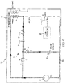
- FIG. 1 depicts a hold-up capacitor charging circuit 10 including a voltage boosting charge pump circuit 20 and a fly-back circuit 40.
- the voltage boosting charge pump circuit 20 selectively charges a hold-up capacitor 24 electrically coupled to a voltage source 26.
- the voltage boosting charge pump circuit 20 includes a flying capacitor 28 that is selectively charged and discharged responsive to fly-back pulses 30 produced by a transformer 42 of the fly-back circuit 40.
- the voltage boosting charge pump circuit 20 can include a first diode 32 electrically coupled to the voltage source 26 and the flying capacitor 28.
- the voltage boosting charge pump circuit 20 can also include a second diode 34 electrically coupled between the first diode 32 and the hold-up capacitor 24.
- the first and second diodes 32, 34 can be used to control the direction of current flow in various operating conditions.
- the hold-up capacitor 24 can be initially charged to a voltage of the voltage source 26 less voltage drops through the first and second diodes 32, 34.
- the flying capacitor 28 can be charged to the voltage of the voltage source 26 less a voltage drop through the first diode 32.
- the voltage provided to the hold-up capacitor 24 is effectively doubled based on the voltage of the voltage source 26 in series with voltage of the flying capacitor 28.
- the fly-back circuit 40 includes a switch 44 electrically coupled to the voltage source 26 and a primary winding 46 of the transformer 42.
- the switch 44 is also electrically coupled to the voltage boosting charge pump circuit 20, where fly-back pulses 30 are produced responsive to a controller 48 changing the open/closed state of the switch 44, for instance, using pulse width modulation.
- the transformer 42 also includes a secondary winding 50 electrically coupled to a load 52.
- a diode 54 may be in series with the load 52, and a capacitor 56 can be in parallel with the load 52.
- the controller 48 is operable to open and close the switch 44 to control energy transfer from the primary winding 46 to the secondary winding 50 and charge the hold-up capacitor 24 responsive to voltages of the voltage source 26, the voltage boosting charge pump circuit 20, and a reflected voltage of the secondary winding 50 at the primary winding 46.
- Control logic of the controller 48 can be implemented by analog circuitry, executable instructions and/or digital circuitry, such as a processing circuit and memory.
- the processing circuit can be embodied in any type of central processing unit (CPU), including a microprocessor, a digital signal processor (DSP), a microcontroller, an application specific integrated circuit (ASIC), a field programmable gate array (FPGA), or the like.
- the memory may include random access memory (RAM), read only memory (ROM), or other electronic, optical, magnetic, or any other computer readable medium onto which is stored data and algorithms as executable instructions in a non-transitory form.
- the controller 48 can output a sequence of pulses (e.g., pulse width modulated pulses) to open and close the switch 44 based on determining that the voltage source 26 exceeds a minimum control voltage.
- the controller 48 controls an output voltage of the secondary winding 50 for the load 52.
- a train of fly-back pulses 30 is generated between the primary winding 46 and the switch 44 based on a reflected voltage from the secondary winding 50.
- the voltage level of the fly-back pulses 30 can be equal to the input voltage of the voltage source 26 plus the reflected voltage from the secondary winding 50.
- Embodiments harvest the fly-back pulses 30, for example, by combining the fly-back pulses 30 with the voltage boosting charge pump circuit 20.
- the voltage across the hold-up capacitor 24 can be boosted to a higher voltage level (e.g., input voltage of the voltage source 26 times two plus the reflected voltage, which is substantially equal to the input voltage of the voltage source 26 plus the voltage level of the fly-back pulses 30).
- FIG. 2 depicts a hold-up capacitor charging circuit 100 illustrating many of the same components as previously described with respect to the hold-up capacitor charging circuit 10 of FIG. 1 .
- the hold-up capacitor charging circuit 100 also includes a resistor 36 electrically coupled between the primary winding 46 and the flying capacitor 28.
- the example of FIG. 2 depicts the switch 44 as a metal-oxide semiconductor field effect transistor (M1 NMOS); however, other types of switching elements are contemplated.
- FIG. 2 illustrates that once an input voltage (Vin) is applied as the voltage source 26, current flows in a first current path 102 through the first diode 32 and the hold-up capacitor 24, initially charging the hold-up capacitor 24 to Vin - 2*Diode Drop (of first diode 32 and second diode 34).
- the controller 48 drives the switch 44.
- the switch 44 When the switch 44 is in a closed state (e.g., ON), currents from Vin flow through the flying capacitor 28 and through primary winding 46 of the transformer 42 as depicted in a second current path 104 of FIG. 3 , charging the flying capacitor 28 to a voltage Vin - Diode Drop (of first diode 32) and storing energy in the primary winding 46 of the transformer 42 of fly-back circuit 40.
- the controller 48 toggles the switch 44 to an open state (e.g., OFF)
- the energy stored in primary winding 46 is transferred to the secondary winding 50.
- the voltage across the primary winding 46 is the reflected voltage from secondary winding 50.
- the input voltage (Vin) from voltage source 26 the secondary reflected primary voltage and voltage stored in flying capacitor 28 are added together since they are connected in series and applied across the hold-up capacitor 24. This boosts voltage across the hold-up capacitor 24, as depicted in the third current path 106 of FIG. 4 .
- the cycle repeats for every OFF-ON (open/closed) cycle of the switch 44.
- the Drop Voltage can include various losses due to series diode drops, DC resistance of the transformer 42, resistance of the switch 44, and/or other factors.
- Table 1 provides examples of results from an embodiment with a turns ratio of 1.5:1 to produce a regulated output of 15 volts. Notably the voltage at holdup capacitor 24 greatly exceeds the input voltage at the voltage source 26.
- a current limiting resistor 37 can be electrically coupled between the second diode 34 and the hold-up capacitor 24 in a current path 202.
- the hold-up capacitor charging circuit 200 may also include a hold-up loading resistor 39 electrically coupled in parallel with the hold-up capacitor 24.
- the combination of the current limiting resistor 37, hold-up capacitor 24, and hold-up loading resistor 39 can filter high frequency components that may result from leakage current of the primary winding 46, and thus prevents high frequency components (e.g., in MHz) from impacting the hold-up voltage at the hold-up capacitor 24.
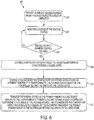
- FIG. 6 depicts a process 300 for hold-up capacitor charging and is described in reference to FIGS. 1-6 .
- an initial charging current is provided from the voltage source 26 to the hold-up capacitor 24 prior to closing the switch 44 (e.g., first current path 102).
- the controller 48 monitors a voltage of the voltage source 26.
- the controller 48 determines whether the voltage of the voltage source 26 exceeds a minimum control voltage. If the voltage of the voltage source 26 does not exceed the minimum control voltage, then the controller 48 continues monitoring the voltage source 26.
- a switch 44 of fly-back circuit 40 is controlled to transition between an open state and a closed state based on determining that the voltage of the voltage source 26 exceeds a minimum control voltage.
- voltage boosting charge pump circuit 20 is charged and energy is stored in a primary winding 46 of transformer 42 of the fly-back circuit 40 based on the controller 48 setting the switch 44 to the closed state (e.g., second current path 104).
- the energy stored in the primary winding 46 is transferred to secondary winding 50 of the transformer 42 to power a load 52 and charge the hold-up capacitor 24 responsive to voltages of the voltage source 26, the voltage boosting charge pump circuit 20, and a reflected voltage of the secondary winding 50 at the primary winding 46 based on the controller 48 setting the switch 44 to the open state (e.g., third current path 106).
- power is supplied from the hold-up capacitor 24 to the voltage source 26 based on a reduction in voltage at the voltage source 26, such as a voltage drop or power loss.
Landscapes
- Engineering & Computer Science (AREA)
- Power Engineering (AREA)
- Dc-Dc Converters (AREA)
Abstract
Description
- This application claims the benefit of the
IN Application No. 201711044598 - Embodiments of the present disclosure relate to electrical power systems, and more particularly, to hold-up capacitor charging using a fly-back power supply.
- Various electronic products make use of a hold-up capacitor to store energy during normal power supply operating conditions. The stored energy is utilized to power up a system for certain duration of time, called the hold-up time, even after the power supply is turned off, either due to a failure condition or a dip in voltage due to overload, etc. During the hold-up time, critical parameter information regarding the status of an electronic unit can be communicated to a next higher level component in a system before the electronic unit shuts down. The hold-up time is proportional to the amount of energy stored in the hold-up capacitor.
- To charge the hold-up capacitor, additional circuitry is typically used, such as an additional high-voltage secondary winding on a transformer with a higher voltage than a typical transformer winding along with rectification circuitry, such that the transformer includes at least three windings (e.g., a primary, a secondary, and a higher-voltage secondary). Other approaches include the addition of a boost converter to generate high voltage with an additional power supply circuit. A boost converter typically includes additional storage elements, such as an inductor, switching circuitry, filtering circuitry, and other components. However, these options result in increased size, power consumption, testing burden, and other such issues.
- Disclosed is a hold-up capacitor charging circuit for a power supply. The hold-up capacitor charging circuit includes a voltage boosting charge pump circuit with a hold-up capacitor electrically coupled to a voltage source, a flying capacitor, a first diode electrically coupled to the voltage source and the flying capacitor, and a second diode electrically coupled between the first diode and the hold-up capacitor. The hold-up capacitor charging circuit also includes a fly-back circuit. The fly-back circuit includes a transformer with a primary winding electrically coupled to the voltage source and a secondary winding electrically coupled to a load. A switch is electrically coupled to the primary winding and the voltage boosting charge pump circuit. A controller is operable to open and close the switch to control energy transfer from the primary winding to the secondary winding and charge the hold-up capacitor responsive to voltages of the voltage source, the voltage boosting charge pump circuit, and a reflected voltage of the secondary winding at the primary winding. The flying capacitor is charged responsive to the voltage source when the switch is closed and the hold-up capacitor voltage is boosted responsive to a fly-back pulse from the transformer when the switch is open, via the flying capacitor.
- In addition to one or more of the features described above, or as an alternative to any of the foregoing embodiments, further embodiments may include a current limiting resistor electrically coupled between the second diode and the hold-up capacitor.
- In addition to one or more of the features described above, or as an alternative to any of the foregoing embodiments, further embodiments may include where the voltage boosting charge pump circuit is operable as a voltage doubling circuit with respect to the voltage source.
- In addition to one or more of the features described above, or as an alternative to any of the foregoing embodiments, further embodiments may include where the controller is a pulse width modulation controller operable to output a sequence of pulses to open and close the switch based on determining that the voltage source exceeds a minimum control voltage.
- In addition to one or more of the features described above, or as an alternative to any of the foregoing embodiments, further embodiments may include where the switch is a metal-oxide semiconductor field effect transistor.
- In addition to one or more of the features described above, or as an alternative to any of the foregoing embodiments, further embodiments may include where the hold-up capacitor is operable to supply power to the voltage source based on a reduction in voltage at the voltage source.
- Also disclosed is a method for hold-up capacitor charging using a fly-back power supply. The method includes monitoring a voltage of a voltage source. A switch of a fly-back circuit is controlled to transition between an open state and a closed state based on determining that the voltage of the voltage source exceeds a minimum control voltage. A voltage boosting charge pump circuit is charged, and energy is stored in a primary winding of a transformer of the fly-back circuit based on the controller setting the switch to the closed state. The voltage boosting charge pump circuit includes a flying capacitor that is charged responsive to the voltage source when the switch is closed, a first diode electrically coupled to the voltage source and the flying capacitor, and a second diode electrically coupled between the first diode and a hold-up capacitor. The energy stored in the primary winding is transferred to a secondary winding of the transformer to power a load, and the hold-up capacitor is charged responsive to voltages of the voltage source, the voltage boosting charge pump circuit, and a reflected voltage of the secondary winding at the primary winding based on the controller setting the switch to the open state.
- In addition to one or more of the features described above, or as an alternative to any of the foregoing embodiments, further embodiments may include providing an initial charging current from the voltage source to the hold-up capacitor prior to closing the switch.
- In addition to one or more of the features described above, or as an alternative to any of the foregoing embodiments, further embodiments may include supplying power from the hold-up capacitor to the voltage source based on a reduction in voltage at the voltage source.
- The subject matter which is regarded as the present disclosure is particularly pointed out and distinctly claimed in the claims at the conclusion of the specification. The foregoing and other features, and advantages of the present disclosure are apparent from the following detailed description taken in conjunction with the accompanying drawings in which:
-
FIG. 1 is a schematic view of a voltage hold-up charging circuit in accordance with an embodiment of the disclosure; -
FIG. 2 is a schematic view of a first current flow path through a portion of a voltage hold-up charging circuit in accordance with an embodiment of the disclosure; -
FIG. 3 is a schematic view of a second current flow path through a portion of a voltage hold-up charging circuit in accordance with an embodiment of the disclosure; -
FIG. 4 is a schematic view of a third current flow path through a portion of a voltage hold-up charging circuit in accordance with an embodiment of the disclosure; -
FIG. 5 is a schematic view of a current flow path through a portion of a voltage hold-up charging circuit in accordance with an embodiment of the disclosure; and -
FIG. 6 is a process flow of a method in accordance with an embodiment of the disclosure. - A detailed description of one or more embodiments of the disclosed apparatus and method are presented herein by way of exemplification and not limitation with reference to the Figures.
- In applications using a fly-back power supply for generating local on-board power supplies, there can be many components that add to system complexity, weight, and size, such as inductors, custom multi-winding transformer, filters, controllers, and the like. When a system requires some type of hold-up circuitry to store energy to be used during a hold-up period, the inclusion of complex additional circuitry for hold-up can add to the overall system complexity, size, and weight. For example, typical hold-up circuitry uses at least two switches that enable a power supply to supply electrical power to both a system load and a hold-up driving & control circuit. In a hold-up condition (e.g., a loss or reduction in voltage output from the power supply), one of the switches can be opened to allow the hold-up driving & control circuit to supply electrical power to the system load. Embodiments reduce the need for additional complex circuitry of a boost converter or an additional winding with rectifier/filter circuit components to charge a hold-up capacitor. For instance, customized magnetics can be avoided as compared to the greater complexities of a multi-winding transformer (e.g., two or more secondary windings).
- Embodiments provide circuitry where a hold-up capacitor is charged using an existing on-board fly-back power supply. In order to boost the charging voltage beyond the input supply voltage, embodiments can make use of few discrete components without using additional complex circuitry. In a capacitor, such as a hold-up capacitor, energy (E) stored is proportional to capacitance (C) and voltage (V) squared to which the capacitor is charged as E = 0.5*C*V2.
- To increase the energy stored in a hold-up capacitor, it can be beneficial to increase the voltage supplied to the hold-up capacitor beyond the voltage supplied directly by a voltage source. In some embodiments, a voltage boosting charge pump circuit, such as a one-level voltage doubling circuit can be included which generates a voltage of 2*Vin, where Vin is the applied input voltage from a voltage source. To further increase voltage, a secondary reflected voltage from a fly-back circuit can also be used in combination with the voltage boosting charge pump circuit, where the secondary reflected voltage on a primary winding and may be expressed as V0*(Npri/Nsec), where V0 is the secondary voltage, Nsec is the number of secondary turns, Npri is the number of primary turns. Additionally, voltage of the primary winding of a fly-back circuit can also be used to charge the hold-up capacitor. Various examples of hold-up capacitor charging circuits are further described herein.
- Turning to the figures,
FIG. 1 depicts a hold-upcapacitor charging circuit 10 including a voltage boostingcharge pump circuit 20 and a fly-back circuit 40. The voltage boostingcharge pump circuit 20 selectively charges a hold-up capacitor 24 electrically coupled to avoltage source 26. The voltage boostingcharge pump circuit 20 includes aflying capacitor 28 that is selectively charged and discharged responsive to fly-back pulses 30 produced by atransformer 42 of the fly-back circuit 40. The voltage boostingcharge pump circuit 20 can include afirst diode 32 electrically coupled to thevoltage source 26 and theflying capacitor 28. The voltage boostingcharge pump circuit 20 can also include asecond diode 34 electrically coupled between thefirst diode 32 and the hold-up capacitor 24. The first andsecond diodes up capacitor 24 can be initially charged to a voltage of thevoltage source 26 less voltage drops through the first andsecond diodes capacitor 28 can be charged to the voltage of thevoltage source 26 less a voltage drop through thefirst diode 32. Under certain operating conditions with respect to the fly-back circuit 40 and responsive to the fly-back pulses 30, the voltage provided to the hold-upcapacitor 24 is effectively doubled based on the voltage of thevoltage source 26 in series with voltage of the flyingcapacitor 28. - The fly-
back circuit 40 includes aswitch 44 electrically coupled to thevoltage source 26 and a primary winding 46 of thetransformer 42. Theswitch 44 is also electrically coupled to the voltage boostingcharge pump circuit 20, where fly-back pulses 30 are produced responsive to acontroller 48 changing the open/closed state of theswitch 44, for instance, using pulse width modulation. Thetransformer 42 also includes a secondary winding 50 electrically coupled to aload 52. Adiode 54 may be in series with theload 52, and acapacitor 56 can be in parallel with theload 52. - In embodiments, the
controller 48 is operable to open and close theswitch 44 to control energy transfer from the primary winding 46 to the secondary winding 50 and charge the hold-upcapacitor 24 responsive to voltages of thevoltage source 26, the voltage boostingcharge pump circuit 20, and a reflected voltage of the secondary winding 50 at the primary winding 46. Control logic of thecontroller 48 can be implemented by analog circuitry, executable instructions and/or digital circuitry, such as a processing circuit and memory. The processing circuit can be embodied in any type of central processing unit (CPU), including a microprocessor, a digital signal processor (DSP), a microcontroller, an application specific integrated circuit (ASIC), a field programmable gate array (FPGA), or the like. Also, in embodiments, the memory may include random access memory (RAM), read only memory (ROM), or other electronic, optical, magnetic, or any other computer readable medium onto which is stored data and algorithms as executable instructions in a non-transitory form. - The
controller 48 can output a sequence of pulses (e.g., pulse width modulated pulses) to open and close theswitch 44 based on determining that thevoltage source 26 exceeds a minimum control voltage. Thecontroller 48 controls an output voltage of the secondary winding 50 for theload 52. As a by-product, a train of fly-back pulses 30 is generated between the primary winding 46 and theswitch 44 based on a reflected voltage from the secondary winding 50. The voltage level of the fly-back pulses 30 can be equal to the input voltage of thevoltage source 26 plus the reflected voltage from the secondary winding 50. - Embodiments harvest the fly-
back pulses 30, for example, by combining the fly-back pulses 30 with the voltage boostingcharge pump circuit 20. By combining the train of fly-back pulses 30 generated in the fly-back circuit 40 and the voltage boostingcharge pump circuit 20, the voltage across the hold-upcapacitor 24 can be boosted to a higher voltage level (e.g., input voltage of thevoltage source 26 times two plus the reflected voltage, which is substantially equal to the input voltage of thevoltage source 26 plus the voltage level of the fly-back pulses 30). -
FIG. 2 depicts a hold-upcapacitor charging circuit 100 illustrating many of the same components as previously described with respect to the hold-upcapacitor charging circuit 10 ofFIG. 1 . The hold-upcapacitor charging circuit 100 also includes aresistor 36 electrically coupled between the primary winding 46 and the flyingcapacitor 28. The example ofFIG. 2 depicts theswitch 44 as a metal-oxide semiconductor field effect transistor (M1 NMOS); however, other types of switching elements are contemplated.FIG. 2 illustrates that once an input voltage (Vin) is applied as thevoltage source 26, current flows in a firstcurrent path 102 through thefirst diode 32 and the hold-upcapacitor 24, initially charging the hold-upcapacitor 24 to Vin - 2*Diode Drop (offirst diode 32 and second diode 34). - Once Vin exceeds a minimum control voltage, the
controller 48 drives theswitch 44. When theswitch 44 is in a closed state (e.g., ON), currents from Vin flow through the flyingcapacitor 28 and through primary winding 46 of thetransformer 42 as depicted in a secondcurrent path 104 ofFIG. 3 , charging the flyingcapacitor 28 to a voltage Vin - Diode Drop (of first diode 32) and storing energy in the primary winding 46 of thetransformer 42 of fly-back circuit 40. - When the
controller 48 toggles theswitch 44 to an open state (e.g., OFF), the energy stored in primary winding 46 is transferred to the secondary winding 50. The voltage across the primary winding 46 is the reflected voltage from secondary winding 50. During OFF time of theswitch 44, the input voltage (Vin) fromvoltage source 26, the secondary reflected primary voltage and voltage stored in flyingcapacitor 28 are added together since they are connected in series and applied across the hold-upcapacitor 24. This boosts voltage across the hold-upcapacitor 24, as depicted in the thirdcurrent path 106 ofFIG. 4 . The cycle repeats for every OFF-ON (open/closed) cycle of theswitch 44. - The voltage obtained at each step is explained through equations below:
- Step 1 :

- Step 2 :

- Step 3 : V(reflected) = V0*(Np/Ns), where Ns and Np are the number of turns in secondary winding 50 and primary winding 46 of
transformer 42, and V0 is the output of the secondary winding 50 (e.g., based on the fly-back design). - The Drop Voltage can include various losses due to series diode drops, DC resistance of the
transformer 42, resistance of theswitch 44, and/or other factors. - Table 1 provides examples of results from an embodiment with a turns ratio of 1.5:1 to produce a regulated output of 15 volts. Notably the voltage at
holdup capacitor 24 greatly exceeds the input voltage at thevoltage source 26.Table 1 - Example results of hold-up capacitor voltages Input Output Holdup V (V) I (A) V (V) V Holdup Test (V) V Holdup Calc (V) 18 0.83 15.12 53.95 54.5 28 0.594 15.142 74.3 74.5 32 0.54 15.154 82.05 82.5 - Additional components can be included in some embodiments. For instance, in the example of hold-up
capacitor charging circuit 200 ofFIG. 5 with similar elements as previously described in reference to hold-upcapacitor charging circuits FIGS. 1-4 , a current limitingresistor 37 can be electrically coupled between thesecond diode 34 and the hold-upcapacitor 24 in acurrent path 202. The hold-upcapacitor charging circuit 200 may also include a hold-up loading resistor 39 electrically coupled in parallel with the hold-upcapacitor 24. The combination of the current limitingresistor 37, hold-upcapacitor 24, and hold-up loading resistor 39 can filter high frequency components that may result from leakage current of the primary winding 46, and thus prevents high frequency components (e.g., in MHz) from impacting the hold-up voltage at the hold-upcapacitor 24. -
FIG. 6 depicts aprocess 300 for hold-up capacitor charging and is described in reference toFIGS. 1-6 . Atblock 302, an initial charging current is provided from thevoltage source 26 to the hold-upcapacitor 24 prior to closing the switch 44 (e.g., first current path 102). At block 304, thecontroller 48 monitors a voltage of thevoltage source 26. Atblock 306, thecontroller 48 determines whether the voltage of thevoltage source 26 exceeds a minimum control voltage. If the voltage of thevoltage source 26 does not exceed the minimum control voltage, then thecontroller 48 continues monitoring thevoltage source 26. Atblock 308, aswitch 44 of fly-back circuit 40 is controlled to transition between an open state and a closed state based on determining that the voltage of thevoltage source 26 exceeds a minimum control voltage. Atblock 310, voltage boostingcharge pump circuit 20 is charged and energy is stored in a primary winding 46 oftransformer 42 of the fly-back circuit 40 based on thecontroller 48 setting theswitch 44 to the closed state (e.g., second current path 104). Atblock 312, the energy stored in the primary winding 46 is transferred to secondary winding 50 of thetransformer 42 to power aload 52 and charge the hold-upcapacitor 24 responsive to voltages of thevoltage source 26, the voltage boostingcharge pump circuit 20, and a reflected voltage of the secondary winding 50 at the primary winding 46 based on thecontroller 48 setting theswitch 44 to the open state (e.g., third current path 106). In embodiments, power is supplied from the hold-upcapacitor 24 to thevoltage source 26 based on a reduction in voltage at thevoltage source 26, such as a voltage drop or power loss. - The term "about" is intended to include the degree of error associated with measurement of the particular quantity based upon the equipment available at the time of filing the application. For example, "about" can include a range of ± 8% or 5%, or 2% of a given value.
- The terminology used herein is for the purpose of describing particular embodiments only and is not intended to be limiting of the present disclosure. As used herein, the singular forms "a", "an" and "the" are intended to include the plural forms as well, unless the context clearly indicates otherwise. It will be further understood that the terms "comprises" and/or "comprising," when used in this specification, specify the presence of stated features, integers, steps, operations, elements, and/or components, but do not preclude the presence or addition of one or more other features, integers, steps, operations, element components, and/or groups thereof.
- While the present disclosure has been described with reference to an exemplary embodiment or embodiments, it will be understood by those skilled in the art that various changes may be made and equivalents may be substituted for elements thereof without departing from the scope of the present disclosure. In addition, many modifications may be made to adapt a particular situation or material to the teachings of the present disclosure without departing from the essential scope thereof. Therefore, it is intended that the present disclosure not be limited to the particular embodiment disclosed as the best mode contemplated for carrying out this present disclosure, but that the present disclosure will include all embodiments falling within the scope of the claims.




Claims (13)
- A hold-up capacitor charging circuit comprising:a voltage boosting charge pump circuit (20) comprising:a hold-up capacitor (24) electrically coupled to a voltage source (26);a flying capacitor (28);a first diode (32) electrically coupled to the voltage source and the flying capacitor; anda second diode (34) electrically coupled between the first diode and the hold-up capacitor; anda fly-back circuit (40) comprising:a transformer (42) comprising a primary winding electrically coupled to the voltage source and a secondary winding electrically coupled to a load;a switch (44) electrically coupled to the primary winding and the voltage boosting charge pump circuit; anda controller (48) operable to open and close the switch to control energy transfer from the primary winding to the secondary winding and charge the hold-up capacitor responsive to voltages of the voltage source, the voltage boosting charge pump circuit, and a reflected voltage of the secondary winding at the primary winding, wherein the flying capacitor is charged responsive to the voltage source when the switch is closed and the hold-up capacitor voltage is boosted responsive to a fly-back pulse from the transformer when the switch is open, via the flying capacitor.
- The hold-up capacitor charging circuit of claim 1, further comprising a current limiting resistor (37) electrically coupled between the second diode and the hold-up capacitor.
- The hold-up capacitor charging circuit of claim 1 or 2, wherein the voltage boosting charge pump circuit is operable as a voltage doubling circuit with respect to the voltage source.
- The hold-up capacitor charging circuit of claim 1, 2 or 3, wherein the controller is a pulse width modulation controller operable to output a sequence of pulses to open and close the switch based on determining that the voltage source exceeds a minimum control voltage.
- The hold-up capacitor charging circuit of any preceding claim, wherein the switch is a metal-oxide semiconductor field effect transistor.
- The hold-up capacitor charging circuit of any preceding claim, wherein the hold-up capacitor is operable to supply power to the voltage source based on a reduction in voltage at the voltage source.
- A method comprising:monitoring a voltage of a voltage source;controlling a switch of a fly-back circuit to transition between an open state and a closed state based on determining that the voltage of the voltage source exceeds a minimum control voltage;charging a voltage boosting charge pump circuit and storing energy in a primary winding of a transformer of the fly-back circuit based on the controller setting the switch to the closed state, wherein the voltage boosting charge pump circuit comprises:a flying capacitor that is charged responsive to the voltage source when the switch is closed;a first diode electrically coupled to the voltage source and the flying capacitor; anda second diode electrically coupled between the first diode and a holdup capacitor;charging the hold-up capacitor responsive to a fly-back pulse from the transformer when the switch is open; andtransferring the energy stored in the primary winding to a secondary winding of the transformer to power a load and charging the hold-up capacitor responsive to voltages of the voltage source, the voltage boosting charge pump circuit, and a reflected voltage of the secondary winding at the primary winding based on the controller setting the switch to the open state.
- The method of claim 7, further comprising providing an initial charging current from the voltage source to the hold-up capacitor prior to closing the switch.
- The method of claim 7 or 8, wherein a current limiting resistor is electrically coupled between the second diode and the hold-up capacitor.
- The method of claim 7, 8 or 9, wherein the voltage boosting charge pump circuit is operable as a voltage doubling circuit with respect to the voltage source.
- The method of any of claims 7 to 10, wherein the controller is a pulse width modulation controller operable to output a sequence of pulses to open and close the switch.
- The method of any of claims 7 to 11, wherein the switch is a metal-oxide semiconductor field effect transistor.
- The method of any of claims 7 to 12, further comprising:supplying power from the hold-up capacitor to the voltage source based on a reduction in voltage at the voltage source.
Applications Claiming Priority (1)
| Application Number | Priority Date | Filing Date | Title |
|---|---|---|---|
| IN201711044598 | 2017-12-12 |
Publications (2)
| Publication Number | Publication Date |
|---|---|
| EP3499702A1 true EP3499702A1 (en) | 2019-06-19 |
| EP3499702B1 EP3499702B1 (en) | 2021-09-01 |
Family
ID=64665001
Family Applications (1)
| Application Number | Title | Priority Date | Filing Date |
|---|---|---|---|
| EP18211910.7A Active EP3499702B1 (en) | 2017-12-12 | 2018-12-12 | Hold-up capacitor charging using fly-back power supply |
Country Status (2)
| Country | Link |
|---|---|
| US (1) | US10277049B1 (en) |
| EP (1) | EP3499702B1 (en) |
Families Citing this family (3)
| Publication number | Priority date | Publication date | Assignee | Title |
|---|---|---|---|---|
| US20240128850A1 (en) * | 2022-10-12 | 2024-04-18 | Hamilton Sundstrand Corporation | Holdup capacitor charging using single switch forward converter |
| US20240128879A1 (en) * | 2022-10-12 | 2024-04-18 | Hamilton Sundstrand Corporation | Holdup capacitor charging using two switch forward converter |
| PL443010A1 (en) * | 2022-11-30 | 2024-06-03 | Waven Spółka Z Ograniczoną Odpowiedzialnością | Self-excited inductively coupled charge pump system |
Citations (2)
| Publication number | Priority date | Publication date | Assignee | Title |
|---|---|---|---|---|
| US20040156217A1 (en) * | 2003-02-10 | 2004-08-12 | Phadke Vijay Gangadhar | Single conversion power converter with hold-up time |
| US20100013548A1 (en) * | 2008-07-18 | 2010-01-21 | Analog Devices, Inc. | Power efficient charge pump with controlled peak currents |
Family Cites Families (9)
| Publication number | Priority date | Publication date | Assignee | Title |
|---|---|---|---|---|
| US6233165B1 (en) * | 2000-05-15 | 2001-05-15 | Asic Advantage, Inc. | Power converter having a low voltage regulator powered from a high voltage source |
| JP2005063820A (en) * | 2003-08-13 | 2005-03-10 | Koito Mfg Co Ltd | Discharge lamp lighting circuit |
| US7265503B2 (en) * | 2004-04-08 | 2007-09-04 | International Rectifier Corporation | Applications of halogen convertor control IC |
| US7589983B1 (en) * | 2005-11-10 | 2009-09-15 | Iwatt Inc. | Power converter controller controlled by variable reference voltage generated by dual output digital to analog converter |
| US8638578B2 (en) * | 2009-08-14 | 2014-01-28 | Power System Technologies, Ltd. | Power converter including a charge pump employable in a power adapter |
| KR101208576B1 (en) * | 2010-08-25 | 2012-12-06 | 주식회사 동부하이텍 | luminous device drive apparatus |
| TWI462456B (en) * | 2012-10-05 | 2014-11-21 | Nat Univ Tsing Hua | Dc/dc converter |
| US20170279349A1 (en) | 2016-03-24 | 2017-09-28 | Linear Technology Corporation | High efficiency charge pump with auxiliary input operative to optimize conversion ratio |
| US10230301B2 (en) * | 2016-12-13 | 2019-03-12 | Rohm Co. Ltd. | Non-isolated DC/DC converter |
-
2018
- 2018-02-06 US US15/889,249 patent/US10277049B1/en active Active
- 2018-12-12 EP EP18211910.7A patent/EP3499702B1/en active Active
Patent Citations (2)
| Publication number | Priority date | Publication date | Assignee | Title |
|---|---|---|---|---|
| US20040156217A1 (en) * | 2003-02-10 | 2004-08-12 | Phadke Vijay Gangadhar | Single conversion power converter with hold-up time |
| US20100013548A1 (en) * | 2008-07-18 | 2010-01-21 | Analog Devices, Inc. | Power efficient charge pump with controlled peak currents |
Also Published As
| Publication number | Publication date |
|---|---|
| US10277049B1 (en) | 2019-04-30 |
| EP3499702B1 (en) | 2021-09-01 |
Similar Documents
| Publication | Publication Date | Title |
|---|---|---|
| US5629844A (en) | High voltage power supply having multiple high voltage generators | |
| US9998022B2 (en) | Current limit peak regulation circuit for power converter with low standby power dissipation | |
| US8148968B2 (en) | Method and apparatus for a power supply controller responsive to a feedforward signal | |
| US9729063B2 (en) | Voltage adjustment system and method for parallel-stage power converter | |
| US9893546B2 (en) | Direct current power supply circuit | |
| US20150280544A1 (en) | Emulated peak current limit scheme for switching regulator | |
| US8711584B2 (en) | Reducing voltage stress in a flyback converter design | |
| EP3499702B1 (en) | Hold-up capacitor charging using fly-back power supply | |
| US10734907B2 (en) | Synchronous rectifier circuit and switching power supply apparatus | |
| US20140119059A1 (en) | Split current mirror line sensing | |
| US12289052B2 (en) | Integrated circuit and power supply circuit | |
| US20200169167A1 (en) | Dc/dc power converter | |
| US7586759B2 (en) | Power source apparatus | |
| WO2014159660A1 (en) | Digital soft start with continuous ramp-up | |
| US20110149619A1 (en) | Method and apparatus for varying current limit to limit an output power of a power supply | |
| US8854850B2 (en) | AC power supply apparatus | |
| JP6908849B2 (en) | Synchronous rectifier circuit and switching power supply | |
| US20180198364A1 (en) | Switching power supply device | |
| US7583521B2 (en) | Over voltage clamp | |
| US20170207699A1 (en) | Switching power supply device | |
| EP2299573A1 (en) | Improving the accuracy of a volt-second clamp in an isolated dc/dc converter | |
| JPH01311864A (en) | Switching type stabilized power supply circuit device | |
| EP3772169B1 (en) | Four-mode tap-switching transformer rectifier | |
| US9923452B2 (en) | Switched-mode power supply for powering a frequency converter | |
| US20210249893A1 (en) | Regulated Storage Capacitor Charging Device and Method |
Legal Events
| Date | Code | Title | Description |
|---|---|---|---|
| PUAI | Public reference made under article 153(3) epc to a published international application that has entered the european phase |
Free format text: ORIGINAL CODE: 0009012 |
|
| STAA | Information on the status of an ep patent application or granted ep patent |
Free format text: STATUS: THE APPLICATION HAS BEEN PUBLISHED |
|
| AK | Designated contracting states |
Kind code of ref document: A1 Designated state(s): AL AT BE BG CH CY CZ DE DK EE ES FI FR GB GR HR HU IE IS IT LI LT LU LV MC MK MT NL NO PL PT RO RS SE SI SK SM TR |
|
| AX | Request for extension of the european patent |
Extension state: BA ME |
|
| STAA | Information on the status of an ep patent application or granted ep patent |
Free format text: STATUS: REQUEST FOR EXAMINATION WAS MADE |
|
| 17P | Request for examination filed |
Effective date: 20191219 |
|
| RBV | Designated contracting states (corrected) |
Designated state(s): AL AT BE BG CH CY CZ DE DK EE ES FI FR GB GR HR HU IE IS IT LI LT LU LV MC MK MT NL NO PL PT RO RS SE SI SK SM TR |
|
| RIN1 | Information on inventor provided before grant (corrected) |
Inventor name: KATAKAM, SRIDHAR Inventor name: LAKSHMI, PRIYA KAKARLA NAGA Inventor name: AGRAWAL, SHOBHIT Inventor name: VALLERU, SOMASEKHAR Inventor name: FERNANDEZ-MATTOS, RODRIGO Inventor name: RAO, SESH MOHAN |
|
| STAA | Information on the status of an ep patent application or granted ep patent |
Free format text: STATUS: EXAMINATION IS IN PROGRESS |
|
| 17Q | First examination report despatched |
Effective date: 20200624 |
|
| GRAP | Despatch of communication of intention to grant a patent |
Free format text: ORIGINAL CODE: EPIDOSNIGR1 |
|
| STAA | Information on the status of an ep patent application or granted ep patent |
Free format text: STATUS: GRANT OF PATENT IS INTENDED |
|
| INTG | Intention to grant announced |
Effective date: 20210331 |
|
| GRAS | Grant fee paid |
Free format text: ORIGINAL CODE: EPIDOSNIGR3 |
|
| GRAA | (expected) grant |
Free format text: ORIGINAL CODE: 0009210 |
|
| STAA | Information on the status of an ep patent application or granted ep patent |
Free format text: STATUS: THE PATENT HAS BEEN GRANTED |
|
| AK | Designated contracting states |
Kind code of ref document: B1 Designated state(s): AL AT BE BG CH CY CZ DE DK EE ES FI FR GB GR HR HU IE IS IT LI LT LU LV MC MK MT NL NO PL PT RO RS SE SI SK SM TR |
|
| REG | Reference to a national code |
Ref country code: GB Ref legal event code: FG4D |
|
| REG | Reference to a national code |
Ref country code: CH Ref legal event code: EP Ref country code: AT Ref legal event code: REF Ref document number: 1427278 Country of ref document: AT Kind code of ref document: T Effective date: 20210915 |
|
| REG | Reference to a national code |
Ref country code: DE Ref legal event code: R096 Ref document number: 602018022749 Country of ref document: DE |
|
| REG | Reference to a national code |
Ref country code: IE Ref legal event code: FG4D |
|
| REG | Reference to a national code |
Ref country code: LT Ref legal event code: MG9D |
|
| REG | Reference to a national code |
Ref country code: NL Ref legal event code: MP Effective date: 20210901 |
|
| PG25 | Lapsed in a contracting state [announced via postgrant information from national office to epo] |
Ref country code: SE Free format text: LAPSE BECAUSE OF FAILURE TO SUBMIT A TRANSLATION OF THE DESCRIPTION OR TO PAY THE FEE WITHIN THE PRESCRIBED TIME-LIMIT Effective date: 20210901 Ref country code: RS Free format text: LAPSE BECAUSE OF FAILURE TO SUBMIT A TRANSLATION OF THE DESCRIPTION OR TO PAY THE FEE WITHIN THE PRESCRIBED TIME-LIMIT Effective date: 20210901 Ref country code: HR Free format text: LAPSE BECAUSE OF FAILURE TO SUBMIT A TRANSLATION OF THE DESCRIPTION OR TO PAY THE FEE WITHIN THE PRESCRIBED TIME-LIMIT Effective date: 20210901 Ref country code: ES Free format text: LAPSE BECAUSE OF FAILURE TO SUBMIT A TRANSLATION OF THE DESCRIPTION OR TO PAY THE FEE WITHIN THE PRESCRIBED TIME-LIMIT Effective date: 20210901 Ref country code: FI Free format text: LAPSE BECAUSE OF FAILURE TO SUBMIT A TRANSLATION OF THE DESCRIPTION OR TO PAY THE FEE WITHIN THE PRESCRIBED TIME-LIMIT Effective date: 20210901 Ref country code: NO Free format text: LAPSE BECAUSE OF FAILURE TO SUBMIT A TRANSLATION OF THE DESCRIPTION OR TO PAY THE FEE WITHIN THE PRESCRIBED TIME-LIMIT Effective date: 20211201 Ref country code: BG Free format text: LAPSE BECAUSE OF FAILURE TO SUBMIT A TRANSLATION OF THE DESCRIPTION OR TO PAY THE FEE WITHIN THE PRESCRIBED TIME-LIMIT Effective date: 20211201 Ref country code: LT Free format text: LAPSE BECAUSE OF FAILURE TO SUBMIT A TRANSLATION OF THE DESCRIPTION OR TO PAY THE FEE WITHIN THE PRESCRIBED TIME-LIMIT Effective date: 20210901 |
|
| REG | Reference to a national code |
Ref country code: AT Ref legal event code: MK05 Ref document number: 1427278 Country of ref document: AT Kind code of ref document: T Effective date: 20210901 |
|
| PG25 | Lapsed in a contracting state [announced via postgrant information from national office to epo] |
Ref country code: PL Free format text: LAPSE BECAUSE OF FAILURE TO SUBMIT A TRANSLATION OF THE DESCRIPTION OR TO PAY THE FEE WITHIN THE PRESCRIBED TIME-LIMIT Effective date: 20210901 Ref country code: LV Free format text: LAPSE BECAUSE OF FAILURE TO SUBMIT A TRANSLATION OF THE DESCRIPTION OR TO PAY THE FEE WITHIN THE PRESCRIBED TIME-LIMIT Effective date: 20210901 Ref country code: GR Free format text: LAPSE BECAUSE OF FAILURE TO SUBMIT A TRANSLATION OF THE DESCRIPTION OR TO PAY THE FEE WITHIN THE PRESCRIBED TIME-LIMIT Effective date: 20211202 |
|
| PG25 | Lapsed in a contracting state [announced via postgrant information from national office to epo] |
Ref country code: AT Free format text: LAPSE BECAUSE OF FAILURE TO SUBMIT A TRANSLATION OF THE DESCRIPTION OR TO PAY THE FEE WITHIN THE PRESCRIBED TIME-LIMIT Effective date: 20210901 |
|
| PG25 | Lapsed in a contracting state [announced via postgrant information from national office to epo] |
Ref country code: IS Free format text: LAPSE BECAUSE OF FAILURE TO SUBMIT A TRANSLATION OF THE DESCRIPTION OR TO PAY THE FEE WITHIN THE PRESCRIBED TIME-LIMIT Effective date: 20220101 Ref country code: SM Free format text: LAPSE BECAUSE OF FAILURE TO SUBMIT A TRANSLATION OF THE DESCRIPTION OR TO PAY THE FEE WITHIN THE PRESCRIBED TIME-LIMIT Effective date: 20210901 Ref country code: SK Free format text: LAPSE BECAUSE OF FAILURE TO SUBMIT A TRANSLATION OF THE DESCRIPTION OR TO PAY THE FEE WITHIN THE PRESCRIBED TIME-LIMIT Effective date: 20210901 Ref country code: RO Free format text: LAPSE BECAUSE OF FAILURE TO SUBMIT A TRANSLATION OF THE DESCRIPTION OR TO PAY THE FEE WITHIN THE PRESCRIBED TIME-LIMIT Effective date: 20210901 Ref country code: PT Free format text: LAPSE BECAUSE OF FAILURE TO SUBMIT A TRANSLATION OF THE DESCRIPTION OR TO PAY THE FEE WITHIN THE PRESCRIBED TIME-LIMIT Effective date: 20220103 Ref country code: NL Free format text: LAPSE BECAUSE OF FAILURE TO SUBMIT A TRANSLATION OF THE DESCRIPTION OR TO PAY THE FEE WITHIN THE PRESCRIBED TIME-LIMIT Effective date: 20210901 Ref country code: EE Free format text: LAPSE BECAUSE OF FAILURE TO SUBMIT A TRANSLATION OF THE DESCRIPTION OR TO PAY THE FEE WITHIN THE PRESCRIBED TIME-LIMIT Effective date: 20210901 Ref country code: CZ Free format text: LAPSE BECAUSE OF FAILURE TO SUBMIT A TRANSLATION OF THE DESCRIPTION OR TO PAY THE FEE WITHIN THE PRESCRIBED TIME-LIMIT Effective date: 20210901 Ref country code: AL Free format text: LAPSE BECAUSE OF FAILURE TO SUBMIT A TRANSLATION OF THE DESCRIPTION OR TO PAY THE FEE WITHIN THE PRESCRIBED TIME-LIMIT Effective date: 20210901 |
|
| REG | Reference to a national code |
Ref country code: DE Ref legal event code: R097 Ref document number: 602018022749 Country of ref document: DE |
|
| PLBE | No opposition filed within time limit |
Free format text: ORIGINAL CODE: 0009261 |
|
| STAA | Information on the status of an ep patent application or granted ep patent |
Free format text: STATUS: NO OPPOSITION FILED WITHIN TIME LIMIT |
|
| PG25 | Lapsed in a contracting state [announced via postgrant information from national office to epo] |
Ref country code: MC Free format text: LAPSE BECAUSE OF FAILURE TO SUBMIT A TRANSLATION OF THE DESCRIPTION OR TO PAY THE FEE WITHIN THE PRESCRIBED TIME-LIMIT Effective date: 20210901 Ref country code: IT Free format text: LAPSE BECAUSE OF FAILURE TO SUBMIT A TRANSLATION OF THE DESCRIPTION OR TO PAY THE FEE WITHIN THE PRESCRIBED TIME-LIMIT Effective date: 20210901 Ref country code: DK Free format text: LAPSE BECAUSE OF FAILURE TO SUBMIT A TRANSLATION OF THE DESCRIPTION OR TO PAY THE FEE WITHIN THE PRESCRIBED TIME-LIMIT Effective date: 20210901 |
|
| REG | Reference to a national code |
Ref country code: CH Ref legal event code: PL |
|
| 26N | No opposition filed |
Effective date: 20220602 |
|
| PG25 | Lapsed in a contracting state [announced via postgrant information from national office to epo] |
Ref country code: SI Free format text: LAPSE BECAUSE OF FAILURE TO SUBMIT A TRANSLATION OF THE DESCRIPTION OR TO PAY THE FEE WITHIN THE PRESCRIBED TIME-LIMIT Effective date: 20210901 |
|
| REG | Reference to a national code |
Ref country code: BE Ref legal event code: MM Effective date: 20211231 |
|
| PG25 | Lapsed in a contracting state [announced via postgrant information from national office to epo] |
Ref country code: LU Free format text: LAPSE BECAUSE OF NON-PAYMENT OF DUE FEES Effective date: 20211212 Ref country code: IE Free format text: LAPSE BECAUSE OF NON-PAYMENT OF DUE FEES Effective date: 20211212 |
|
| PG25 | Lapsed in a contracting state [announced via postgrant information from national office to epo] |
Ref country code: BE Free format text: LAPSE BECAUSE OF NON-PAYMENT OF DUE FEES Effective date: 20211231 |
|
| PG25 | Lapsed in a contracting state [announced via postgrant information from national office to epo] |
Ref country code: LI Free format text: LAPSE BECAUSE OF NON-PAYMENT OF DUE FEES Effective date: 20211231 Ref country code: CH Free format text: LAPSE BECAUSE OF NON-PAYMENT OF DUE FEES Effective date: 20211231 |
|
| P01 | Opt-out of the competence of the unified patent court (upc) registered |
Effective date: 20230522 |
|
| PG25 | Lapsed in a contracting state [announced via postgrant information from national office to epo] |
Ref country code: CY Free format text: LAPSE BECAUSE OF FAILURE TO SUBMIT A TRANSLATION OF THE DESCRIPTION OR TO PAY THE FEE WITHIN THE PRESCRIBED TIME-LIMIT Effective date: 20210901 |
|
| PG25 | Lapsed in a contracting state [announced via postgrant information from national office to epo] |
Ref country code: HU Free format text: LAPSE BECAUSE OF FAILURE TO SUBMIT A TRANSLATION OF THE DESCRIPTION OR TO PAY THE FEE WITHIN THE PRESCRIBED TIME-LIMIT; INVALID AB INITIO Effective date: 20181212 |
|
| PG25 | Lapsed in a contracting state [announced via postgrant information from national office to epo] |
Ref country code: MK Free format text: LAPSE BECAUSE OF FAILURE TO SUBMIT A TRANSLATION OF THE DESCRIPTION OR TO PAY THE FEE WITHIN THE PRESCRIBED TIME-LIMIT Effective date: 20210901 |
|
| PG25 | Lapsed in a contracting state [announced via postgrant information from national office to epo] |
Ref country code: MT Free format text: LAPSE BECAUSE OF FAILURE TO SUBMIT A TRANSLATION OF THE DESCRIPTION OR TO PAY THE FEE WITHIN THE PRESCRIBED TIME-LIMIT Effective date: 20210901 |
|
| PG25 | Lapsed in a contracting state [announced via postgrant information from national office to epo] |
Ref country code: TR Free format text: LAPSE BECAUSE OF FAILURE TO SUBMIT A TRANSLATION OF THE DESCRIPTION OR TO PAY THE FEE WITHIN THE PRESCRIBED TIME-LIMIT Effective date: 20210901 |
|
| PGFP | Annual fee paid to national office [announced via postgrant information from national office to epo] |
Ref country code: DE Payment date: 20251126 Year of fee payment: 8 |
|
| PGFP | Annual fee paid to national office [announced via postgrant information from national office to epo] |
Ref country code: GB Payment date: 20251119 Year of fee payment: 8 |
|
| PGFP | Annual fee paid to national office [announced via postgrant information from national office to epo] |
Ref country code: FR Payment date: 20251120 Year of fee payment: 8 |