EP3499648A1 - Connector structure - Google Patents
Connector structure Download PDFInfo
- Publication number
- EP3499648A1 EP3499648A1 EP18206897.3A EP18206897A EP3499648A1 EP 3499648 A1 EP3499648 A1 EP 3499648A1 EP 18206897 A EP18206897 A EP 18206897A EP 3499648 A1 EP3499648 A1 EP 3499648A1
- Authority
- EP
- European Patent Office
- Prior art keywords
- housing
- case body
- cover
- terminal part
- connector
- Prior art date
- Legal status (The legal status is an assumption and is not a legal conclusion. Google has not performed a legal analysis and makes no representation as to the accuracy of the status listed.)
- Withdrawn
Links
- 239000000758 substrate Substances 0.000 claims abstract description 45
- 230000002093 peripheral effect Effects 0.000 claims description 20
- 238000004519 manufacturing process Methods 0.000 abstract description 3
- 238000000465 moulding Methods 0.000 description 4
- 238000005476 soldering Methods 0.000 description 3
- 238000010586 diagram Methods 0.000 description 2
- 230000002708 enhancing effect Effects 0.000 description 2
- 230000015572 biosynthetic process Effects 0.000 description 1
- 230000004048 modification Effects 0.000 description 1
- 238000012986 modification Methods 0.000 description 1
- 230000035515 penetration Effects 0.000 description 1
- 230000008961 swelling Effects 0.000 description 1
Images




Classifications
-
- H—ELECTRICITY
- H01—ELECTRIC ELEMENTS
- H01R—ELECTRICALLY-CONDUCTIVE CONNECTIONS; STRUCTURAL ASSOCIATIONS OF A PLURALITY OF MUTUALLY-INSULATED ELECTRICAL CONNECTING ELEMENTS; COUPLING DEVICES; CURRENT COLLECTORS
- H01R13/00—Details of coupling devices of the kinds covered by groups H01R12/70 or H01R24/00 - H01R33/00
- H01R13/46—Bases; Cases
- H01R13/502—Bases; Cases composed of different pieces
- H01R13/5025—Bases; Cases composed of different pieces one or more pieces being of resilient material
-
- H—ELECTRICITY
- H01—ELECTRIC ELEMENTS
- H01R—ELECTRICALLY-CONDUCTIVE CONNECTIONS; STRUCTURAL ASSOCIATIONS OF A PLURALITY OF MUTUALLY-INSULATED ELECTRICAL CONNECTING ELEMENTS; COUPLING DEVICES; CURRENT COLLECTORS
- H01R12/00—Structural associations of a plurality of mutually-insulated electrical connecting elements, specially adapted for printed circuits, e.g. printed circuit boards [PCB], flat or ribbon cables, or like generally planar structures, e.g. terminal strips, terminal blocks; Coupling devices specially adapted for printed circuits, flat or ribbon cables, or like generally planar structures; Terminals specially adapted for contact with, or insertion into, printed circuits, flat or ribbon cables, or like generally planar structures
- H01R12/50—Fixed connections
- H01R12/51—Fixed connections for rigid printed circuits or like structures
- H01R12/55—Fixed connections for rigid printed circuits or like structures characterised by the terminals
- H01R12/57—Fixed connections for rigid printed circuits or like structures characterised by the terminals surface mounting terminals
-
- H—ELECTRICITY
- H01—ELECTRIC ELEMENTS
- H01R—ELECTRICALLY-CONDUCTIVE CONNECTIONS; STRUCTURAL ASSOCIATIONS OF A PLURALITY OF MUTUALLY-INSULATED ELECTRICAL CONNECTING ELEMENTS; COUPLING DEVICES; CURRENT COLLECTORS
- H01R12/00—Structural associations of a plurality of mutually-insulated electrical connecting elements, specially adapted for printed circuits, e.g. printed circuit boards [PCB], flat or ribbon cables, or like generally planar structures, e.g. terminal strips, terminal blocks; Coupling devices specially adapted for printed circuits, flat or ribbon cables, or like generally planar structures; Terminals specially adapted for contact with, or insertion into, printed circuits, flat or ribbon cables, or like generally planar structures
- H01R12/70—Coupling devices
- H01R12/7005—Guiding, mounting, polarizing or locking means; Extractors
- H01R12/7011—Locking or fixing a connector to a PCB
- H01R12/7052—Locking or fixing a connector to a PCB characterised by the locating members
-
- H—ELECTRICITY
- H01—ELECTRIC ELEMENTS
- H01R—ELECTRICALLY-CONDUCTIVE CONNECTIONS; STRUCTURAL ASSOCIATIONS OF A PLURALITY OF MUTUALLY-INSULATED ELECTRICAL CONNECTING ELEMENTS; COUPLING DEVICES; CURRENT COLLECTORS
- H01R12/00—Structural associations of a plurality of mutually-insulated electrical connecting elements, specially adapted for printed circuits, e.g. printed circuit boards [PCB], flat or ribbon cables, or like generally planar structures, e.g. terminal strips, terminal blocks; Coupling devices specially adapted for printed circuits, flat or ribbon cables, or like generally planar structures; Terminals specially adapted for contact with, or insertion into, printed circuits, flat or ribbon cables, or like generally planar structures
- H01R12/70—Coupling devices
- H01R12/71—Coupling devices for rigid printing circuits or like structures
- H01R12/712—Coupling devices for rigid printing circuits or like structures co-operating with the surface of the printed circuit or with a coupling device exclusively provided on the surface of the printed circuit
- H01R12/716—Coupling device provided on the PCB
-
- H—ELECTRICITY
- H01—ELECTRIC ELEMENTS
- H01R—ELECTRICALLY-CONDUCTIVE CONNECTIONS; STRUCTURAL ASSOCIATIONS OF A PLURALITY OF MUTUALLY-INSULATED ELECTRICAL CONNECTING ELEMENTS; COUPLING DEVICES; CURRENT COLLECTORS
- H01R12/00—Structural associations of a plurality of mutually-insulated electrical connecting elements, specially adapted for printed circuits, e.g. printed circuit boards [PCB], flat or ribbon cables, or like generally planar structures, e.g. terminal strips, terminal blocks; Coupling devices specially adapted for printed circuits, flat or ribbon cables, or like generally planar structures; Terminals specially adapted for contact with, or insertion into, printed circuits, flat or ribbon cables, or like generally planar structures
- H01R12/70—Coupling devices
- H01R12/71—Coupling devices for rigid printing circuits or like structures
- H01R12/72—Coupling devices for rigid printing circuits or like structures coupling with the edge of the rigid printed circuits or like structures
- H01R12/722—Coupling devices for rigid printing circuits or like structures coupling with the edge of the rigid printed circuits or like structures coupling devices mounted on the edge of the printed circuits
- H01R12/727—Coupling devices presenting arrays of contacts
-
- H—ELECTRICITY
- H01—ELECTRIC ELEMENTS
- H01R—ELECTRICALLY-CONDUCTIVE CONNECTIONS; STRUCTURAL ASSOCIATIONS OF A PLURALITY OF MUTUALLY-INSULATED ELECTRICAL CONNECTING ELEMENTS; COUPLING DEVICES; CURRENT COLLECTORS
- H01R13/00—Details of coupling devices of the kinds covered by groups H01R12/70 or H01R24/00 - H01R33/00
- H01R13/46—Bases; Cases
- H01R13/516—Means for holding or embracing insulating body, e.g. casing, hoods
-
- H—ELECTRICITY
- H01—ELECTRIC ELEMENTS
- H01R—ELECTRICALLY-CONDUCTIVE CONNECTIONS; STRUCTURAL ASSOCIATIONS OF A PLURALITY OF MUTUALLY-INSULATED ELECTRICAL CONNECTING ELEMENTS; COUPLING DEVICES; CURRENT COLLECTORS
- H01R13/00—Details of coupling devices of the kinds covered by groups H01R12/70 or H01R24/00 - H01R33/00
- H01R13/66—Structural association with built-in electrical component
- H01R13/665—Structural association with built-in electrical component with built-in electronic circuit
-
- H—ELECTRICITY
- H05—ELECTRIC TECHNIQUES NOT OTHERWISE PROVIDED FOR
- H05K—PRINTED CIRCUITS; CASINGS OR CONSTRUCTIONAL DETAILS OF ELECTRIC APPARATUS; MANUFACTURE OF ASSEMBLAGES OF ELECTRICAL COMPONENTS
- H05K5/00—Casings, cabinets or drawers for electric apparatus
- H05K5/0026—Casings, cabinets or drawers for electric apparatus provided with connectors and printed circuit boards [PCB], e.g. automotive electronic control units
- H05K5/0047—Casings, cabinets or drawers for electric apparatus provided with connectors and printed circuit boards [PCB], e.g. automotive electronic control units having a two-part housing enclosing a PCB
- H05K5/006—Casings, cabinets or drawers for electric apparatus provided with connectors and printed circuit boards [PCB], e.g. automotive electronic control units having a two-part housing enclosing a PCB characterized by features for holding the PCB within the housing
-
- H—ELECTRICITY
- H01—ELECTRIC ELEMENTS
- H01R—ELECTRICALLY-CONDUCTIVE CONNECTIONS; STRUCTURAL ASSOCIATIONS OF A PLURALITY OF MUTUALLY-INSULATED ELECTRICAL CONNECTING ELEMENTS; COUPLING DEVICES; CURRENT COLLECTORS
- H01R12/00—Structural associations of a plurality of mutually-insulated electrical connecting elements, specially adapted for printed circuits, e.g. printed circuit boards [PCB], flat or ribbon cables, or like generally planar structures, e.g. terminal strips, terminal blocks; Coupling devices specially adapted for printed circuits, flat or ribbon cables, or like generally planar structures; Terminals specially adapted for contact with, or insertion into, printed circuits, flat or ribbon cables, or like generally planar structures
- H01R12/70—Coupling devices
- H01R12/71—Coupling devices for rigid printing circuits or like structures
- H01R12/72—Coupling devices for rigid printing circuits or like structures coupling with the edge of the rigid printed circuits or like structures
- H01R12/722—Coupling devices for rigid printing circuits or like structures coupling with the edge of the rigid printed circuits or like structures coupling devices mounted on the edge of the printed circuits
- H01R12/724—Coupling devices for rigid printing circuits or like structures coupling with the edge of the rigid printed circuits or like structures coupling devices mounted on the edge of the printed circuits containing contact members forming a right angle
-
- H—ELECTRICITY
- H01—ELECTRIC ELEMENTS
- H01R—ELECTRICALLY-CONDUCTIVE CONNECTIONS; STRUCTURAL ASSOCIATIONS OF A PLURALITY OF MUTUALLY-INSULATED ELECTRICAL CONNECTING ELEMENTS; COUPLING DEVICES; CURRENT COLLECTORS
- H01R2201/00—Connectors or connections adapted for particular applications
- H01R2201/26—Connectors or connections adapted for particular applications for vehicles
-
- H—ELECTRICITY
- H05—ELECTRIC TECHNIQUES NOT OTHERWISE PROVIDED FOR
- H05K—PRINTED CIRCUITS; CASINGS OR CONSTRUCTIONAL DETAILS OF ELECTRIC APPARATUS; MANUFACTURE OF ASSEMBLAGES OF ELECTRICAL COMPONENTS
- H05K5/00—Casings, cabinets or drawers for electric apparatus
- H05K5/0026—Casings, cabinets or drawers for electric apparatus provided with connectors and printed circuit boards [PCB], e.g. automotive electronic control units
- H05K5/0043—Casings, cabinets or drawers for electric apparatus provided with connectors and printed circuit boards [PCB], e.g. automotive electronic control units comprising a frame housing mating with two lids wherein the PCB is flat mounted on the frame housing
Definitions
- the present invention relates to a connector structure.
- FIG. 7 is a diagram explaining the assembling of a switch provided with a conventional connector structure.
- an electronic component is provided with an electronic substrate 700 and a case 100.
- the case 100 is provided with a case body 110 for accommodating the electronic substrate 700 therein and a cover 150 for closing an opening of the case body 110.
- a connector 500 at the electronic component side is provided with a terminal part 510 supporting a plurality of terminals and a tubular housing 550 surrounding tip end sides of the plurality of terminals.
- a connector (unillustrated) at a vehicle side is inserted from an opened tip end side of the housing, and is connected to a connector at the electronic component side.
- the terminal part 510 of the connector 500 and the housing 550 are usually formed integrally, but a separate formation of the terminal part 510 and the housing 550 has been proposed for cutting down on manufacturing costs.
- the terminal part 510 and the housing 550 are formed separately and the housing 550 is formed to be integral with the case body 110.
- the terminal part 510 is in advance fixed on the electronic substrate 700 by soldering or the like, and then the electronic substrate 700 is accommodated in the inside of the case body 110 from the opening of the case body 110.
- the electronic substrate 700 and the case body 110 are positioned by respective positioning parts 110a, 700a to be mounted.
- the opening of the case body is covered with the cover 150, preventing intrusion of dusts and the like.
- each positional accuracy possibly gets lower as compared to a case of being integrally formed.
- the positional accuracy of the terminal part 510 and the housing 550 is reduced, at the time of inserting the connector at the vehicle side from the tip end of the housing 550 to be connected to the terminal part 510 of the connector 500, there is a possibility that required positional accuracy cannot be achieved.
- the case body 110 For enhancing the positional accuracy of the terminal part 510 and the housing 550, it is considered to cause the case body 110, which has been positioned with respect to the electronic substrate 700, to be positioned directly with respect to the terminal part 510. However, in that case, there is a possibility that the positional accuracy of the case body 110 and the electronic substrate 700 is reduced to reduce positional accuracy of the electronic component of the switch or the like.
- the present invention is made in view of the above-described problems, and an object of the present invention is to provide a connector structure that prevents positional accuracy of a housing and a terminal part for a connector attached to a switch and positional accuracy of an electronic component from being reduced while reducing manufacturing costs of the switch.
- a connector structure in a case in which a connector is attached comprises:
- the terminal part and the housing for the connector are separately disposed, and the housing is not formed to be integral with the case body configuring a function of the electronic component, but is formed to be integral with the cover that covers the opening of the case body for protection from an outside environment. Further, the terminal part and the housing are respectively provided with the positioning parts for the positioning with each other.
- separately forming the terminal part and the housing enables a reduction in costs. Since it is possible to directly position the terminal part and the housing, a reduction in positional accuracy of the terminal part and the housing can be prevented to easily secure the positional accuracy required for connection to the connector at the vehicle side. Further, since the case body is not formed to be integral with the housing, the case body can be directly positioned with respect to the electronic substrate, making it possible to prevent the reduction in the positional accuracy of the electronic component, too.
- a connector structure in a case in which a connector is attached according to an embodiment in the present invention.
- the case configures an electronic component, and the electronic component is not limited to a specific component, and an explanation of the embodiment will be made using an example of a switch that is installed in a vehicle.
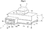
- Fig. 1 is a perspective view illustrating an assembled state of a switch.
- Fig. 2 is an exploded perspective view of the switch.
- Fig. 3 is an exploded cross section illustrating the switch, as viewed from a direction of Y axis of the switch. However, in Fig. 3 , illustration of a knob is omitted.
- a switch as an electronic component is provided with a case 1 that accommodates therein an electronic substrate on which switch elements and the like are installed, and a knob 3 that is held in the case 1 and switches an on/off operation of the switch.
- a connector 5 is attached on the case 1 to connect the switch to a power source, a control device or the like installed at a vehicle side. An explanation of the embodiment will be made using an example where the connector 5 attached on the case 1 is a male connector.
- the case 1 is provided with a boxy case body 11 a lower end of which is opened, and a plate-shaped cover 15 that closes a lower end opening 11a of the case body 11.
- an upper side is defined as an upper direction and a lower side is defined as a lower direction in Fig. 2 , and, based thereupon, a positional relation of the respective elements of the switch will be explained.
- an axis line along an assembling direction of the switch is defined as "axis line X" and an axis line in a direction perpendicular to the axis line X is defined as "axis line Y".
- the case body 11 and the cover 15 each are formed by molding or the like.
- the case body 11 accommodates the electronic substrate 7 therein and is fixed on an unillustrated vehicle body (fixed member).
- the electronic substrate 7 is provided thereon with various components configuring the electronic component, such as switching elements, LEDs and the like.
- a projection 12 that is a positioning part with respect to the electronic substrate 7 is formed on an inner upper surface 11c of the case body 11 (refer to Fig. 3 ).
- the electronic substrate 7 is provided with a plurality of holes 71, 73 that are positioning parts with respect to other members including the case body 11.
- a holding part 13 of the knob 3 is disposed on an outer upper surface 11b of the case body 11.
- the knob 3 is a tubular member an upper end of which is closed and a lower end of which is opened, and a pressing part 31 is disposed on its lower end.
- the pressing part 31 is formed in a position corresponding to the switching element installed on the electronic substrate 7.
- the knob 3 is held in the holding part 13 of the case body 11. By pressing down an upper end surface 3a of the knob 3, the knob 3 slides toward the inside of the case body 11 to cause the pressing part 31 in the lower end of the knob 3 to press the switching element, thus switching an on/off operation of the switch.
- the switching element is provided with a resilient member of a rubber sheet or the like, and when the upper end surface 3a of the knob 3 is released, the knob 3 is urged by the resilient member to be returned back to an initial position.
- the connector 5 is provided with a terminal part 51 for supporting a plurality of pin-shaped terminals 9 and a housing 55 for accommodating the terminal part 51 therein.
- the terminal part 51 and the housing 55 are separately formed, and the housing 55 is formed to be integral with the cover 15 by molding or the like.
- the terminal part 51 is a rectangular terminal platform, and the plurality of pin-shaped terminals 9 arranged along the axis line Y are supported by penetration of them through side surfaces 51a, 51a, which are opposed to each other, of the terminal part 51.
- Projections 52, 52 are formed on an upper surface 51c of the terminal part 51 in the vicinity of both ends thereof in the axis line Y direction.
- the projection 52 is a positioning part with respect to the electronic substrate 7.
- a through hole 53a and a groove 53b are respectively formed in the vicinities of the projections 52, 52.
- the through hole 53a penetrates from the upper surface 51c over a lower surface 51 d of the terminal part 51.
- the groove 53b is formed on a side surface 51b connecting the side surfaces 51a, 51a, and extends along the axis line X from the upper surface 51c to the lower surface 51d.
- the through hole 53a and the groove 53b are positioning parts with the housing 55.
- both ends of the plurality of pin-shaped terminals 9 each project from the side surfaces 51a, 51a, which are opposed to each other, of the terminal part 51, are bent at the right angle toward the upper surface 51c of the terminal part 51, extend to a position of the upper surface 51c of the terminal part 51, and thereafter, extend horizontally along the axis line Y.
- One horizontal part 91 extending horizontally along the axis line Y is longer than the other horizontal part 92.
- a base end section of each of the horizontal parts 91, 92 is earth-connected to the electronic substrate 7.
- a tip end of the longer horizontal part 91 projects outward from an outer edge of the electronic substrate 7, and a female connector is connected to this tip end.
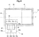
- Fig. 4 is a plan view illustrating the housing formed to be integral with the cover.
- the cover 15 is provided with a rectangular flat surface part 16 that extends along the axis line Y to cover the lower end opening 11a of the case body 11, and a peripheral wall 17 that is disposed to extend upward along the axis line X from an outer edge of the flat surface part 16 and extends to the case body 11-side.
- a stage 18 is disposed on the flat surface part 16 to support the electronic substrate 7. Part of the electronic substrate 7 is supported on the stage 18 and the rest extends on the flat surface part 16 to face the flat surface part 16 by an interval.
- the peripheral wall 17 of the cover 15 faces an inner side surface 11d of the case body 11 in the vicinity of the lower end opening 11a. Since a dimension of the outer edge of the flat surface part 16 is set to be smaller than that of an outer edge of the lower end opening 11a of the case body 11, the peripheral wall 17 of the cover 15 faces the inner side surface 11d of the case body 11 with a gap D1 (refer to Fig. 6 ).
- a flange 20 is disposed to extend horizontally with respect to the flat surface part 16 over an entire circumference of the outer edge of the flat surface part 16 of the cover 15. As illustrated in Fig.1 , the flange 20 covers the gap D1 between the inner side surface 11d of the case body 11 and the peripheral wall 17 of the cover 15. Since the flange 20 is only required to be as long as to cover the gap D1, the flange 20 may have the same dimension as an outer side surface 11e of the case body 11 or may be longer than that.
- the housing 55 is provided with a support part 56 that supports the terminal part 51 and a tubular part 58 that surrounds a tip end side of the horizontal part 91 of the pin-shaped terminal 9.
- the support part 56 is a recessed part formed on the flat surface part 16 of the cover 15, and the lower surface 51d of the terminal part 51 is placed and supported on the support part 56 (refer to Fig. 6 ).
- the support part 56 is provided with projections 57a, 57b that are positioning parts with respect to the terminal part 51.
- the projection 57b is formed in the form of swelling in the axis line Y direction from the peripheral wall 17 of the cover 15.
- the tubular part 58 is formed to extend outward from the outer edge of the flat surface part 16 of the cover 15. It should be noted that the peripheral wall 17 of the cover 15 and the flange 20 as described before are formed in sections other than the tubular part 58.
- a base end 58a-side, which is in contact with the outer edge of the flat surface part 16, of the tubular part 58 and a tip end 58b-side, which opposes the base end 58a, of the tubular part 58 are opened.
- a notch 59 is formed in the base end 58a-side of the outer upper surface 58c of the tubular part 58.
- Fig. 5A is a perspective view illustrating the tubular part and the extension part in the assembling state of the switch
- Fig. 5B is a perspective view illustrating the extension part alone.
- the periphery of the tip end of the pin-shaped terminal 9 is surrounded by the tubular part 58, but a terminal of the female connector is connectable from an exterior of the switch through the opened tip end 58b of the tubular part 58.
- a guide 60 is formed on an inner lower part 58d of the tubular part 58 to guide the terminal of the female connector to the pin-shaped terminal 9.
- the case body 11 is formed in a boxy shape, but a section of the side surface, which faces the tubular part 58, of the housing 55 extends outward along the tubular part 58 to form an extension part 14 covering the outer periphery of the tubular part 58.
- the extension part 14 covers part of the exterior upper surface 58c and the exterior side surfaces 58e, 58e of the tubular part 58, and is formed in a reverse-C letter shape as viewed in section.
- a dimension of the outer periphery of the tubular part 59 of the connector 5 is made smaller than a dimension of an inner periphery of the extension part 14. Therefore the extension part 14 covers the tubular part 58 through a gap D2.
- a plurality of ribs 21 are formed on an inner upper surface 14a and an inner side surface 14b configuring the inner periphery of the extension part 14. As illustrated in Fig. 5A , these ribs 21 respectively extend in the gap D2 to come in contact with the tubular part 58.
- a convex part 22 is formed on the inner upper surface 14a of the extension part 14 facing the outer upper surface 58c of the tubular part 58 to be fitted in the notch 59 (refer to Fig. 2 ) of the tubular part 58.
- the cover 15 and the housing 55 for the connector 5 are formed to be integral by molding or the like, and then, the terminal part 51 of the connector 5, the electronic substrate 7 and the case body 11 are assembled thereto. It should be noted that the knob 3 is held by the holding part 13 of the case body 11, but the details thereof are omitted.
- the terminal part 51 of the connector 5 is fixed on the electronic substrate 7 before assembling the entire switch.
- the projection 52 formed on the upper surface 51c of the terminal part 51 is inserted in a hole 71 of the electronic substrate 7 for the positioning.
- the base end sections of the horizontal parts 91, 92 of the pin-shaped terminal 9 are fixed on the electronic substrate 7 by soldering or the like.
- the tip end of the longer horizontal part 91 of the pin-shaped terminal 9 is placed to extend outward from the outer edge of the electronic substrate 7.
- the electronic substrate 7 and the terminal part 51 that are fixed are assembled to the cover 15 and the housing 55 that are formed to be integral.
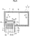
- Fig. 6 is a cross section taken along a Y axis direction and illustrating the assembled state of the switch.
- the electronic substrate 7 is illustrated in a broken line for easy understanding.
- the projections 57, 57 disposed in the support part 56 of the housing 55 are inserted in the through hole 53a and the groove 53b formed in the terminal part 51 for the positioning.
- the tip end of the pin-shaped terminal 9 supported in the terminal part 51 is accommodated in the inside of the tubular part 58 through the notch 59 of the tubular part 58.
- the terminal part 51 and the electronic substrate 7 are assembled to the cover 15 formed to be integral with the housing 55.
- the case body 11 will be assembled to the cover 15.
- the projection 12 disposed on the inner upper surface 11c of the case body 11 is inserted in a hole 73 of the electronic substrate 7 to be positioned, and the convex part 22 formed on the inner upper surface 14a of the extension part 14 is fitted in the notch 59 formed in the outer upper surface 58c of the tubular part 58.
- the flat surface part 16 of the cover 15 is assembled to cover the lower end opening 11a of the case body 11.
- the extension part 14 of the case body 11 covers the tubular part 58 of the housing 55 formed to be integral with the cover 15.
- the cover 15 and the case body 11 are not assembled to be directly positioned.
- the cover 15 and the case body 11 are assembled to be indirectly positioned in the form where the housing 55 of the connector 5 formed to be integral with the cover 15 and the terminal part 51 are positioned and the electronic substrate 7 in advance fixed in the terminal part 51 is positioned in the case body 11. Therefore in a case where the cover 15 and the case body 11 are assembled without a gap, when the peripheral wall 17 of the cover 15 and the inner side surface 11d of the case body 11 have variations in dimension, there is a possibility that they interfere with each other to block the assembling thereof.
- the dimension of the peripheral wall 17 of the cover 15 is made smaller than the dimension of the inner side surface 11d of the case body 11 to cause the peripheral wall 17 of the cover 15 to face the inner side surface 11d of the case body 11 through the gap D1.
- the flange 20 is disposed to extend outward from the outer edge of the cover 15, and by covering the gap D1 between the peripheral wall 17 and the inner side surface 11d of the case body 11 with the flange 20, dusts can be prevented from entering the gap D1.
- the inner periphery of the extension 14 of the case body 11 faces the outer periphery of the tubular part 58 with the gap D2, but as illustrated in Fig. 5 , the plurality of ribs 21 disposed on the inner upper surface 14a and the inner side surface 14b of the extension part 14 extend in the gap D2 to come in contact with the tubular part 58, thus acting as gap fillings.
- a height of each of the ribs 21 is adjusted by a metallic mold.
- the tubular part 58 of the housing 55 since the tubular part 58 of the housing 55 is in contact with the ribs 21, the prying force applied on the housing 55 tends to be easily scattered to the case body 11 fixed to the vehicle body through the ribs 21, making it possible to reduce the prying force that will be input to the terminal part 51.
- a snap fit or the like may be disposed to the cover 15 and the case body 11 to fix the cover 15 to the case body 11.
- the connector structure according to the embodiment is the connector structure in the case 1 in which the connector 5 is attached, wherein, the case 1 includes:
- the housing 550 of the connector 500 is formed to be integral with the case body 110.
- the housing 550 and the terminal part 510 are indirectly positioned through the case body 110 and the electronic substrate 700 respectively connected thereto.
- the cost can be reduced, but on assembling the whole, the positional accuracy of each possibly reduces.
- the positional accuracy of the housing 550 and the terminal part 510 reduces, at the time the female connector at the vehicle side is inserted from the tip end of the tubular part of the housing 550 to be connected to the pin-shaped terminal, the positional accuracy required cannot be possibly achieved.
- the case body110 which has been positioned with respect to the electronic substrate 700, to be positioned directly with respect to the terminal part 510.
- the positional accuracy of the case body 110 and the electronic substrate 700 is reduced to reduce positional accuracy of the electronic component of the switch or the like.
- the housing 55 of the connector 5 is not formed to be integral with the case body 11 configuring the function of the switch as the electronic component, but is formed to be integral with the cover 15 that covers the lower end opening 11a of the case body 11 for protection from the outside environment, thus directly positioning the terminal part 51 and the housing 55.
- the terminal part 51 and the housing 55 are separately formed to reduce the cost while being capable of preventing the reduction in positional accuracy of the terminal part 51 and the housing 55.
- the positional accuracy required in the connection to the connector 5 at the vehicle side is more likely to be secured.
- the case body 11 since the case body 11 is not formed to be integral with the housing 55, the case body 11 can be directly positioned with respect to the electronic substrate 7, also preventing a reduction in positional accuracy of the electronic component.
- the positioning part is only required to be capable of positioning the respective members with respect to each other, and the configuration and the disposed position can be changed as needed. Also as to the positioning part of the other member, the configuration and the disposed position are not limited to specific ones.
- the example of disposing the ribs 21 on the inner periphery of the extension part 14 is explained as an example of the projection, but the projection is not limited to this example.
- the projection is only required to project from somewhere of the inner periphery of the extension part 14 or the outer periphery of the tubular part 58 to cause the inner periphery of the extension part 14 to come in contact with the outer periphery of the tubular part 58.
- a projection in a semispherical shape may be disposed as the projection.
- the projection is not disposed on the inner peripheral side of the extension part 14, but may be disposed on the outer peripheral side of the tubular part 58.
- the cover 15 and the case body 11 are not directly positioned. Therefore in a case where the cover 15 and the case body 11 are to be assembled without a gap, when the peripheral wall 17 disposed to rise in the upward direction from the outer edge of the cover 15 and the inner side surface 11d of the case body 11 have variations in dimension, there is a possibility that the cover 15 and the case body 11 interfere with each other to block the assembling thereof. Therefore, the gap D1 is provided between the peripheral wall 17 of the cover 15 and the inner side surface 11d of the case body 11 to prevent the interference between the cover 15 and the case body 11. Further, the flange 20 is disposed to extend outward from the outer edge of the cover 15, and by covering the gap D1 between the peripheral wall 17 and inner side surface 11d of the case body 11 with the flange 20, dusts can be prevented from entering the gap D1.
Landscapes
- Engineering & Computer Science (AREA)
- Microelectronics & Electronic Packaging (AREA)
- Details Of Connecting Devices For Male And Female Coupling (AREA)
- Coupling Device And Connection With Printed Circuit (AREA)
Abstract
There is provided a connector structure that prevents positional accuracy of a housing 55 and a terminal part 51 for a connector attached to a switch and positional accuracy of an electronic component from being reduced while reducing manufacturing costs of the switch.
A case 1 includes a case body 11 for accommodating an electronic substrate 7 therein and a cover 15 for closing a lower end opening of the case body 11. A connector 5 includes a terminal part 51 for supporting a pin-shaped terminal and a housing 55 including a tubular part for surrounding a tip end side 58a of the pin-shaped terminal. The terminal part 51 and the housing 55 are separately disposed, the terminal part is 51 fixed on the electronic substrate 7, the housing 55 is formed to be integral with the cover 15, and the terminal part 51 and the housing 55 are respectively provided with a through hole 53a and a groove 53b, and projections 57 for positioning the terminal part 51 and the housing 55 with each other.
Description
- The present invention relates to a connector structure.
- An electronic component of a switch or the like that is mounted on a vehicle is connected electrically to a battery, a control device and the like at a vehicle side using a connector (for example, refer to
WO2017/032638 ).
Fig. 7 is a diagram explaining the assembling of a switch provided with a conventional connector structure. - As illustrated in
Fig. 7 , an electronic component is provided with anelectronic substrate 700 and acase 100. Thecase 100 is provided with acase body 110 for accommodating theelectronic substrate 700 therein and acover 150 for closing an opening of thecase body 110. Aconnector 500 at the electronic component side is provided with aterminal part 510 supporting a plurality of terminals and atubular housing 550 surrounding tip end sides of the plurality of terminals. A connector (unillustrated) at a vehicle side is inserted from an opened tip end side of the housing, and is connected to a connector at the electronic component side. - The
terminal part 510 of theconnector 500 and thehousing 550 are usually formed integrally, but a separate formation of theterminal part 510 and thehousing 550 has been proposed for cutting down on manufacturing costs. In the example inFig. 7 , theterminal part 510 and thehousing 550 are formed separately and thehousing 550 is formed to be integral with thecase body 110. Theterminal part 510 is in advance fixed on theelectronic substrate 700 by soldering or the like, and then theelectronic substrate 700 is accommodated in the inside of thecase body 110 from the opening of thecase body 110. Theelectronic substrate 700 and thecase body 110 are positioned byrespective positioning parts cover 150, preventing intrusion of dusts and the like. - In a case where the
terminal part 510 of theconnector 500 and thehousing 550 are separately formed, since theterminal part 510 of theconnector 500 and thehousing 550 are positioned through theelectronic substrate 700 and thecase body 110 connected thereto respectively, each positional accuracy possibly gets lower as compared to a case of being integrally formed. When the positional accuracy of theterminal part 510 and thehousing 550 is reduced, at the time of inserting the connector at the vehicle side from the tip end of thehousing 550 to be connected to theterminal part 510 of theconnector 500, there is a possibility that required positional accuracy cannot be achieved. - For enhancing the positional accuracy of the
terminal part 510 and thehousing 550, it is considered to cause thecase body 110, which has been positioned with respect to theelectronic substrate 700, to be positioned directly with respect to theterminal part 510. However, in that case, there is a possibility that the positional accuracy of thecase body 110 and theelectronic substrate 700 is reduced to reduce positional accuracy of the electronic component of the switch or the like. - Accordingly, the present invention is made in view of the above-described problems, and an object of the present invention is to provide a connector structure that prevents positional accuracy of a housing and a terminal part for a connector attached to a switch and positional accuracy of an electronic component from being reduced while reducing manufacturing costs of the switch.
- According to an aspect of the present invention, a connector structure in a case in which a connector is attached comprises:
- the case including:
- a case body for accommodating an electronic substrate therein; and
- a cover for closing an opening of the case body, wherein
- the connector includes:
- a terminal part for supporting a plurality of terminals; and
- a housing including a tubular part for surrounding tip end sides of the plurality of terminals,
- the terminal part and the housing are separately disposed,
- the terminal part is fixed on the electronic substrate,
- the housing is formed to be integral with the cover, and
- the terminal part and the housing are respectively provided with positioning parts for positioning the terminal part and the housing with each other.
- According to the aspect of the present invention, the terminal part and the housing for the connector are separately disposed, and the housing is not formed to be integral with the case body configuring a function of the electronic component, but is formed to be integral with the cover that covers the opening of the case body for protection from an outside environment. Further, the terminal part and the housing are respectively provided with the positioning parts for the positioning with each other. As a result, separately forming the terminal part and the housing enables a reduction in costs. Since it is possible to directly position the terminal part and the housing, a reduction in positional accuracy of the terminal part and the housing can be prevented to easily secure the positional accuracy required for connection to the connector at the vehicle side. Further, since the case body is not formed to be integral with the housing, the case body can be directly positioned with respect to the electronic substrate, making it possible to prevent the reduction in the positional accuracy of the electronic component, too.
- Other objects, features, and advantages of the present invention will become more apparent from the following detailed description made with reference to the accompanying drawings, in which like parts are designated by like reference numbers and in which:
-
Fig. 1 is a perspective view illustrating the configuration of an outer appearance of a switch according to an embodiment in the present invention, -
Fig. 2 is an exploded perspective view illustrating the switch according to the embodiment, -
Fig. 3 is an exploded cross section illustrating the switch according to the embodiment, as viewed from a direction of Y axis of the switch, -
Fig. 4 is a plan view illustrating a housing formed to be integral with a cover according to the embodiment, -
Fig. 5A is a perspective view illustrating a tubular part and an extension part of the switch in an assembled state of the switch according to the embodiment, -
Fig. 5B is a perspective view illustrating only the extension part of the switch in the assembled state of the switch according to the embodiment, -
Fig. 6 is a cross section taken along Y axis of the switch and illustrating the assemble state of the switch according to the embodiment, and -
Fig. 7 is a diagram explaining the assembling of a switch provided with a conventional connector structure. - Hereinafter, an explanation will be made of a connector structure in a case in which a connector is attached according to an embodiment in the present invention. The case configures an electronic component, and the electronic component is not limited to a specific component, and an explanation of the embodiment will be made using an example of a switch that is installed in a vehicle.
-
Fig. 1 is a perspective view illustrating an assembled state of a switch. -
Fig. 2 is an exploded perspective view of the switch. -
Fig. 3 is an exploded cross section illustrating the switch, as viewed from a direction of Y axis of the switch. However, inFig. 3 , illustration of a knob is omitted. - As illustrated in
Fig. 1 andFig. 2 , a switch as an electronic component is provided with acase 1 that accommodates therein an electronic substrate on which switch elements and the like are installed, and aknob 3 that is held in thecase 1 and switches an on/off operation of the switch. Aconnector 5 is attached on thecase 1 to connect the switch to a power source, a control device or the like installed at a vehicle side. An explanation of the embodiment will be made using an example where theconnector 5 attached on thecase 1 is a male connector. - The
case 1 is provided with aboxy case body 11 a lower end of which is opened, and a plate-shaped cover 15 that closes a lower end opening 11a of thecase body 11. It should be noted that, for descriptive purposes, an upper side is defined as an upper direction and a lower side is defined as a lower direction inFig. 2 , and, based thereupon, a positional relation of the respective elements of the switch will be explained. In addition, an axis line along an assembling direction of the switch is defined as "axis line X" and an axis line in a direction perpendicular to the axis line X is defined as "axis line Y". - The
case body 11 and thecover 15 each are formed by molding or the like. Thecase body 11 accommodates theelectronic substrate 7 therein and is fixed on an unillustrated vehicle body (fixed member). Although unillustrated, theelectronic substrate 7 is provided thereon with various components configuring the electronic component, such as switching elements, LEDs and the like. Aprojection 12 that is a positioning part with respect to theelectronic substrate 7 is formed on an innerupper surface 11c of the case body 11 (refer toFig. 3 ). In addition, theelectronic substrate 7 is provided with a plurality ofholes case body 11. - A holding
part 13 of theknob 3 is disposed on an outerupper surface 11b of thecase body 11. Theknob 3 is a tubular member an upper end of which is closed and a lower end of which is opened, and apressing part 31 is disposed on its lower end. Thepressing part 31 is formed in a position corresponding to the switching element installed on theelectronic substrate 7. - The
knob 3 is held in the holdingpart 13 of thecase body 11. By pressing down anupper end surface 3a of theknob 3, theknob 3 slides toward the inside of thecase body 11 to cause thepressing part 31 in the lower end of theknob 3 to press the switching element, thus switching an on/off operation of the switch. The switching element is provided with a resilient member of a rubber sheet or the like, and when theupper end surface 3a of theknob 3 is released, theknob 3 is urged by the resilient member to be returned back to an initial position. - The
connector 5 is provided with aterminal part 51 for supporting a plurality of pin-shapedterminals 9 and ahousing 55 for accommodating theterminal part 51 therein. Theterminal part 51 and thehousing 55 are separately formed, and thehousing 55 is formed to be integral with thecover 15 by molding or the like. - The
terminal part 51 is a rectangular terminal platform, and the plurality of pin-shapedterminals 9 arranged along the axis line Y are supported by penetration of them throughside surfaces terminal part 51.Projections upper surface 51c of theterminal part 51 in the vicinity of both ends thereof in the axis line Y direction. Theprojection 52 is a positioning part with respect to theelectronic substrate 7. A throughhole 53a and agroove 53b are respectively formed in the vicinities of theprojections hole 53a penetrates from theupper surface 51c over alower surface 51 d of theterminal part 51. Thegroove 53b is formed on aside surface 51b connecting the side surfaces 51a, 51a, and extends along the axis line X from theupper surface 51c to thelower surface 51d. The throughhole 53a and thegroove 53b are positioning parts with thehousing 55. - As illustrated in
Fig. 3 , both ends of the plurality of pin-shapedterminals 9 each project from the side surfaces 51a, 51a, which are opposed to each other, of theterminal part 51, are bent at the right angle toward theupper surface 51c of theterminal part 51, extend to a position of theupper surface 51c of theterminal part 51, and thereafter, extend horizontally along the axis line Y. Onehorizontal part 91 extending horizontally along the axis line Y is longer than the otherhorizontal part 92. InFig. 3 , as surrounded by circles, a base end section of each of thehorizontal parts electronic substrate 7. A tip end of the longerhorizontal part 91 projects outward from an outer edge of theelectronic substrate 7, and a female connector is connected to this tip end. -
Fig. 4 is a plan view illustrating the housing formed to be integral with the cover. - As illustrated in
Fig. 2 andFig. 4 , thecover 15 is provided with a rectangularflat surface part 16 that extends along the axis line Y to cover thelower end opening 11a of thecase body 11, and aperipheral wall 17 that is disposed to extend upward along the axis line X from an outer edge of theflat surface part 16 and extends to the case body 11-side. Astage 18 is disposed on theflat surface part 16 to support theelectronic substrate 7. Part of theelectronic substrate 7 is supported on thestage 18 and the rest extends on theflat surface part 16 to face theflat surface part 16 by an interval. - As illustrated in
Fig. 1 , in a state where thecase body 11 and thecover 15 are assembled, theperipheral wall 17 of thecover 15 faces aninner side surface 11d of thecase body 11 in the vicinity of thelower end opening 11a. Since a dimension of the outer edge of theflat surface part 16 is set to be smaller than that of an outer edge of thelower end opening 11a of thecase body 11, theperipheral wall 17 of thecover 15 faces theinner side surface 11d of thecase body 11 with a gap D1 (refer toFig. 6 ). - A
flange 20 is disposed to extend horizontally with respect to theflat surface part 16 over an entire circumference of the outer edge of theflat surface part 16 of thecover 15. As illustrated inFig.1 , theflange 20 covers the gap D1 between theinner side surface 11d of thecase body 11 and theperipheral wall 17 of thecover 15. Since theflange 20 is only required to be as long as to cover the gap D1, theflange 20 may have the same dimension as anouter side surface 11e of thecase body 11 or may be longer than that. - The
housing 55 is provided with asupport part 56 that supports theterminal part 51 and atubular part 58 that surrounds a tip end side of thehorizontal part 91 of the pin-shapedterminal 9. - The
support part 56 is a recessed part formed on theflat surface part 16 of thecover 15, and thelower surface 51d of theterminal part 51 is placed and supported on the support part 56 (refer toFig. 6 ). Thesupport part 56 is provided withprojections terminal part 51. Theprojection 57b is formed in the form of swelling in the axis line Y direction from theperipheral wall 17 of thecover 15. When theprojection 57a is inserted in the throughhole 53a of theterminal part 51 and theprojection 57b is inserted in thegroove 53b, theterminal part 51 and thehousing 55 are positioned. - As illustrated in
Fig. 2 , thetubular part 58 is formed to extend outward from the outer edge of theflat surface part 16 of thecover 15. It should be noted that theperipheral wall 17 of thecover 15 and theflange 20 as described before are formed in sections other than thetubular part 58. - A
base end 58a-side, which is in contact with the outer edge of theflat surface part 16, of thetubular part 58 and atip end 58b-side, which opposes thebase end 58a, of thetubular part 58 are opened. Anotch 59 is formed in thebase end 58a-side of the outerupper surface 58c of thetubular part 58. At the time of assembling theterminal part 51 on thehousing 55, the tip end of thehorizontal part 91 of the pin-shapedterminal 9 supported by theterminal part 51 is caused to be accommodated in the inside of thetubular part 58 through thenotch 59 of thetubular part 58. -
Fig. 5A is a perspective view illustrating the tubular part and the extension part in the assembling state of the switch, andFig. 5B is a perspective view illustrating the extension part alone. - As illustrated in
Fig. 5A , the periphery of the tip end of the pin-shapedterminal 9 is surrounded by thetubular part 58, but a terminal of the female connector is connectable from an exterior of the switch through the openedtip end 58b of thetubular part 58. Aguide 60 is formed on an innerlower part 58d of thetubular part 58 to guide the terminal of the female connector to the pin-shapedterminal 9. - As described before, the
case body 11 is formed in a boxy shape, but a section of the side surface, which faces thetubular part 58, of thehousing 55 extends outward along thetubular part 58 to form anextension part 14 covering the outer periphery of thetubular part 58. Theextension part 14 covers part of the exteriorupper surface 58c and the exterior side surfaces 58e, 58e of thetubular part 58, and is formed in a reverse-C letter shape as viewed in section. - A dimension of the outer periphery of the
tubular part 59 of theconnector 5 is made smaller than a dimension of an inner periphery of theextension part 14. Therefore theextension part 14 covers thetubular part 58 through a gap D2. As illustrated inFig. 5B , a plurality ofribs 21 are formed on an innerupper surface 14a and aninner side surface 14b configuring the inner periphery of theextension part 14. As illustrated inFig. 5A , theseribs 21 respectively extend in the gap D2 to come in contact with thetubular part 58. Aconvex part 22 is formed on the innerupper surface 14a of theextension part 14 facing the outerupper surface 58c of thetubular part 58 to be fitted in the notch 59 (refer toFig. 2 ) of thetubular part 58. - An explanation will be made of the assembling and the operation of the switch having the above-mentioned configuration.
- As described before, the
cover 15 and thehousing 55 for theconnector 5 are formed to be integral by molding or the like, and then, theterminal part 51 of theconnector 5, theelectronic substrate 7 and thecase body 11 are assembled thereto. It should be noted that theknob 3 is held by the holdingpart 13 of thecase body 11, but the details thereof are omitted. - As illustrated in
Fig. 3 , theterminal part 51 of theconnector 5 is fixed on theelectronic substrate 7 before assembling the entire switch. Theprojection 52 formed on theupper surface 51c of theterminal part 51 is inserted in ahole 71 of theelectronic substrate 7 for the positioning. - As illustrated by the round surroundings in
Fig. 3 , the base end sections of thehorizontal parts terminal 9 are fixed on theelectronic substrate 7 by soldering or the like. The tip end of the longerhorizontal part 91 of the pin-shapedterminal 9 is placed to extend outward from the outer edge of theelectronic substrate 7. - Next, the
electronic substrate 7 and theterminal part 51 that are fixed are assembled to thecover 15 and thehousing 55 that are formed to be integral. -
Fig. 6 is a cross section taken along a Y axis direction and illustrating the assembled state of the switch. InFig. 6 , theelectronic substrate 7 is illustrated in a broken line for easy understanding. - As illustrated in
Fig. 3 andFig. 6 , theprojections support part 56 of thehousing 55 are inserted in the throughhole 53a and thegroove 53b formed in theterminal part 51 for the positioning. The tip end of the pin-shapedterminal 9 supported in theterminal part 51 is accommodated in the inside of thetubular part 58 through thenotch 59 of thetubular part 58. Thereby theterminal part 51 and theelectronic substrate 7 are assembled to thecover 15 formed to be integral with thehousing 55. - Subsequently the
case body 11 will be assembled to thecover 15. Theprojection 12 disposed on the innerupper surface 11c of thecase body 11 is inserted in ahole 73 of theelectronic substrate 7 to be positioned, and theconvex part 22 formed on the innerupper surface 14a of theextension part 14 is fitted in thenotch 59 formed in the outerupper surface 58c of thetubular part 58. Thereby theflat surface part 16 of thecover 15 is assembled to cover thelower end opening 11a of thecase body 11. Theextension part 14 of thecase body 11 covers thetubular part 58 of thehousing 55 formed to be integral with thecover 15. - That is, in the embodiment the
cover 15 and thecase body 11 are not assembled to be directly positioned. Thecover 15 and thecase body 11 are assembled to be indirectly positioned in the form where thehousing 55 of theconnector 5 formed to be integral with thecover 15 and theterminal part 51 are positioned and theelectronic substrate 7 in advance fixed in theterminal part 51 is positioned in thecase body 11. Therefore in a case where thecover 15 and thecase body 11 are assembled without a gap, when theperipheral wall 17 of thecover 15 and theinner side surface 11d of thecase body 11 have variations in dimension, there is a possibility that they interfere with each other to block the assembling thereof. Therefore the dimension of theperipheral wall 17 of thecover 15 is made smaller than the dimension of theinner side surface 11d of thecase body 11 to cause theperipheral wall 17 of thecover 15 to face theinner side surface 11d of thecase body 11 through the gap D1. Further, theflange 20 is disposed to extend outward from the outer edge of thecover 15, and by covering the gap D1 between theperipheral wall 17 and theinner side surface 11d of thecase body 11 with theflange 20, dusts can be prevented from entering the gap D1. - The inner periphery of the
extension 14 of thecase body 11 faces the outer periphery of thetubular part 58 with the gap D2, but as illustrated inFig. 5 , the plurality ofribs 21 disposed on the innerupper surface 14a and theinner side surface 14b of theextension part 14 extend in the gap D2 to come in contact with thetubular part 58, thus acting as gap fillings. When some of the plurality ofribs 21 do not come in contact with theextension 14 due to a dimension tolerance, a height of each of theribs 21 is adjusted by a metallic mold. - When the female connector at the vehicle side is inserted from the
tip end 58b of thetubular part 58 of thehousing 55 in theconnector 5 to be connected to the pin-shapedterminal 9 of theterminal part 51, a prying force is applied on thehousing 55. When the prying force is input on theterminal part 51 connected to thehousing 55 by the positioning to be applied on sections (sections surrounded by circles inFig. 3 ) of theterminal part 51 soldered to theelectronic substrate 7, a reduction in quality of theconnector 5 is possibly invited. In the embodiment, since thetubular part 58 of thehousing 55 is in contact with theribs 21, the prying force applied on thehousing 55 tends to be easily scattered to thecase body 11 fixed to the vehicle body through theribs 21, making it possible to reduce the prying force that will be input to theterminal part 51. - It should be noted that, although not illustrated, a snap fit or the like may be disposed to the
cover 15 and thecase body 11 to fix thecover 15 to thecase body 11. - As described above, the connector structure according to the embodiment is the connector structure in the
case 1 in which theconnector 5 is attached, wherein,
thecase 1 includes: - the
case body 11 for accommodating theelectronic substrate 7 therein; and - the
cover 15 for closing thelower end opening 11a (opening) of thecase body 11, - the
connector 5 includes:- the
terminal part 51 for supporting the plurality of terminals 9 (terminals); and - the
housing 55 including thetubular part 58 for surrounding tip end sides of the plurality ofterminals 9, - the
terminal part 51 and thehousing 55 are separately disposed, - the
terminal part 51 is fixed on theelectronic substrate 7, - the
housing 55 is formed to be integral with thecover 15, and - the
terminal part 51 and thehousing 55 are respectively provided with the throughhole 53a and thegroove 53b, and theprojections 57, 57 (positioning parts) for positioning theterminal part 51 and thehousing 55 with each other.
- the
- According to the conventional connector structure (refer to
Fig. 7 ), thehousing 550 of theconnector 500 is formed to be integral with thecase body 110. On assembling, thehousing 550 and theterminal part 510 are indirectly positioned through thecase body 110 and theelectronic substrate 700 respectively connected thereto. As compared to a case where thehousing 550 and theterminal part 510 are integrally formed, the cost can be reduced, but on assembling the whole, the positional accuracy of each possibly reduces. When the positional accuracy of thehousing 550 and theterminal part 510 reduces, at the time the female connector at the vehicle side is inserted from the tip end of the tubular part of thehousing 550 to be connected to the pin-shaped terminal, the positional accuracy required cannot be possibly achieved. - For enhancing the positional accuracy of the
terminal part 510 and thehousing 550, it is considered to cause the case body110, which has been positioned with respect to theelectronic substrate 700, to be positioned directly with respect to theterminal part 510. However, in that case, there is a possibility that the positional accuracy of thecase body 110 and theelectronic substrate 700 is reduced to reduce positional accuracy of the electronic component of the switch or the like. - In the connector structure according to the embodiment illustrated in
Fig. 1 to Fig. 6 , thehousing 55 of theconnector 5 is not formed to be integral with thecase body 11 configuring the function of the switch as the electronic component, but is formed to be integral with thecover 15 that covers thelower end opening 11a of thecase body 11 for protection from the outside environment, thus directly positioning theterminal part 51 and thehousing 55. Thereby theterminal part 51 and thehousing 55 are separately formed to reduce the cost while being capable of preventing the reduction in positional accuracy of theterminal part 51 and thehousing 55. Thereby the positional accuracy required in the connection to theconnector 5 at the vehicle side is more likely to be secured. Further, since thecase body 11 is not formed to be integral with thehousing 55, thecase body 11 can be directly positioned with respect to theelectronic substrate 7, also preventing a reduction in positional accuracy of the electronic component. - It should be noted that in the embodiment, the example of using the through
hole 53a and theterminal part 51 and thegroove 53b, and theprojections terminal part 51 and thehousing 55 is explained, but the positioning part is only required to be capable of positioning the respective members with respect to each other, and the configuration and the disposed position can be changed as needed. Also as to the positioning part of the other member, the configuration and the disposed position are not limited to specific ones. - (2) The
case body 11 is fixed on the vehicle body (fixed member) and is provided with theextension part 14 for covering at least part of the outer periphery of thetubular part 58 of thehousing 55, and the innerupper surface 11c and theinner side surface 11d (inner periphery), which face the outer periphery of thehousing 55 through the gap D2, of theextension part 14 are provided with the ribs 21 (projections) in contact with the outer periphery of thetubular part 58 of thehousing 55. - When the female connector at the vehicle side is inserted from the tip end of the
tubular part 58 of thehousing 55 of theconnector 5 to be connected to the pin-shapedterminal 9 of theterminal part 51, the prying force is applied on thehousing 55, but thetubular part 58 of thehousing 55 comes in contact with theribs 21 to act as the gap fillings. Thereby the prying force applied to thehousing 55 tends to be easily scattered to thecase body 11 fixed on the vehicle body through theribs 21. Thereby it is possible to reduce the prying force that is input to theterminal part 51 to be applied to the section of theterminal part 51 and theelectronic substrate 7 fixed by soldering, making it possible to prevent the reduction in quality of theconnector 5. In addition, when some of theribs 21 do not come in contact with the outer periphery of theextension part 14 due to the dimension tolerance, the height of each of theribs 21 can be adjusted by the metallic molding. - It should be noted that in the embodiment, the example of disposing the
ribs 21 on the inner periphery of theextension part 14 is explained as an example of the projection, but the projection is not limited to this example. The projection is only required to project from somewhere of the inner periphery of theextension part 14 or the outer periphery of thetubular part 58 to cause the inner periphery of theextension part 14 to come in contact with the outer periphery of thetubular part 58. For example, a projection in a semispherical shape may be disposed as the projection. In addition, the projection is not disposed on the inner peripheral side of theextension part 14, but may be disposed on the outer peripheral side of thetubular part 58. - (3) The
cover 15 is provided with theflat surface part 16 that covers thelower end opening 11a of thecase body 11, theperipheral wall 17 that extends to the case body 11-side from the outer edge of theflat surface part 16 and faces theinner side surface 11d (inner periphery) of thecase body 11 with the gap D1, and theflange 20 that is disposed over the entire circumference of the outer edge of theflat surface part 16 and extends in the horizontal direction with respect to theflat surface part 16 to cover the gap D1 between theinner side surface 11d of thecase body 11 and theperipheral wall 17 of thecover 15. - In the embodiment the
cover 15 and thecase body 11 are not directly positioned. Therefore in a case where thecover 15 and thecase body 11 are to be assembled without a gap, when theperipheral wall 17 disposed to rise in the upward direction from the outer edge of thecover 15 and theinner side surface 11d of thecase body 11 have variations in dimension, there is a possibility that thecover 15 and thecase body 11 interfere with each other to block the assembling thereof. Therefore, the gap D1 is provided between theperipheral wall 17 of thecover 15 and theinner side surface 11d of thecase body 11 to prevent the interference between thecover 15 and thecase body 11. Further, theflange 20 is disposed to extend outward from the outer edge of thecover 15, and by covering the gap D1 between theperipheral wall 17 andinner side surface 11d of thecase body 11 with theflange 20, dusts can be prevented from entering the gap D1. - While only the selected embodiment has been chosen to illustrate the present invention, it will be apparent to those skilled in the art from this disclosure that various changes and modifications can be made therein without departing from the scope of the invention as defined in the appended claims. Furthermore, the foregoing description of the embodiment according to the present invention is provided for illustration only, and not for the purpose of limiting the invention as defined by the appended claims and their equivalents.
-
- 1 CASE
- 3 KNOB
- 3a UPPER END SURFACE
- 5 CONNECTOR
- 7 ELECTRONIC SUBSTRATE
- 9 PIN-SHAPED TERMINAL
- 11 CASE BODY
- 11a LOWER END OPENING
- 11b OUTER UPPER SURFACE
- 11c INNER UPPER SURFACE
- 11d INNER SIDE SURFACE
- 11 e OUTER SIDE SURFACE
- 12 PROJECTION
- 13 HOLDING PART
- 14 EXTENSION PART
- 14a INNER UPPER SURFACE
- 14b INNER SIDE SURFACE
- 15 COVER
- 16 FLAT SURFACE PART
- 17 PERIPHERAL WALL
- 18 STAGE
- 20 FLANGE
- 21 RIB
- 22 CONVEX PART
- 31 PRESSING PART
- 51 TERMINAL PART
- 51a, 51a SIDE SURFACE
- 51b SIDE SURFACE
- 51c UPPER SURFACE
- 51d LOWER SURFACE
- 52 PROJECTION
- 53a THROUGH HOLE
- 53b GROOVE
- 55 HOUSING
- 56 SUPPORT PART
- 57 PROJECTION
- 58 TUBULAR PART
- 58a BASE END
- 58b TIP END
- 58c OUTER UPPER SURFACE
- 58d INNER LOWER SURFACE
- 58e OUTER SIDE SURFACE
- 59 NOTCH
- 60 GUIDE
- 71, 73 HOLE
- 91, 92 HORIZONTAL PART
- D1, D2 GAP
Claims (3)
- A connector structure in a case (1) in which a connector (5) is attached, wherein
the case (1) includes:a case body (11) for accommodating an electronic substrate (7) therein; anda cover (15) for closing an opening of the case body (11),the connector includes:a terminal part (51) for supporting a plurality of terminals; anda housing (55) including a tubular part (58) for surrounding tip end sides (58a) of the plurality of terminals,the terminal part (51) and the housing (55) are separately disposed,the terminal part (51) is fixed on the electronic substrate (7),the housing (55) is formed to be integral with the cover (15), andthe terminal part (51) and the housing (55) are respectively provided with positioning parts for positioning the terminal part (51) and the housing (55) with each other. - The connector structure according to claim 1, wherein
the case body (11) includes an extension part (14) that is fixed on a fixed member and covers at least part of an outer periphery of the housing (55), and
an inner periphery of the extension part (14) or the outer periphery of the housing (55) facing the inner periphery of the extension part through a gap (D1, D2) includes a projection (12) causing the inner periphery of the extension part (14) to be in contact with the outer periphery of the housing (55). - The connector structure according to claim 1, wherein
the cover (15) includes:a flat surface part (16) that covers an opening of the case body (11);a peripheral wall (17) that extends to the case body side from an outer edge of the flat surface part (16) and faces an inner periphery of the case body (11) through a gap (D1, D2); anda flange (20) that is disposed over an entire circumference of the outer edge of the flat surface part (16) and extends in a horizontal direction with respect to the flat surface part (16) to cover the gap (D1, D2) between the inner periphery of the case body (11) and the peripheral wall of the cover (15).
Applications Claiming Priority (1)
| Application Number | Priority Date | Filing Date | Title |
|---|---|---|---|
| JP2017241924A JP2019110018A (en) | 2017-12-18 | 2017-12-18 | Connector structure |
Publications (1)
| Publication Number | Publication Date |
|---|---|
| EP3499648A1 true EP3499648A1 (en) | 2019-06-19 |
Family
ID=64362369
Family Applications (1)
| Application Number | Title | Priority Date | Filing Date |
|---|---|---|---|
| EP18206897.3A Withdrawn EP3499648A1 (en) | 2017-12-18 | 2018-11-19 | Connector structure |
Country Status (5)
| Country | Link |
|---|---|
| US (1) | US20190190186A1 (en) |
| EP (1) | EP3499648A1 (en) |
| JP (1) | JP2019110018A (en) |
| CN (1) | CN109994849A (en) |
| CA (1) | CA3024797A1 (en) |
Cited By (1)
| Publication number | Priority date | Publication date | Assignee | Title |
|---|---|---|---|---|
| EP4207501A1 (en) * | 2021-12-31 | 2023-07-05 | Tyco Electronics (Suzhou) Co. Ltd. | Connector and connector assembly |
Families Citing this family (3)
| Publication number | Priority date | Publication date | Assignee | Title |
|---|---|---|---|---|
| DE102020116501A1 (en) | 2020-06-23 | 2021-12-23 | Valeo Schalter Und Sensoren Gmbh | Circuit board with connection elements for contact pins of different pin headers |
| US12170465B2 (en) | 2021-02-03 | 2024-12-17 | Black & Decker Inc. | Electronic power module |
| CN115734536A (en) * | 2022-11-04 | 2023-03-03 | 蔚来汽车科技(安徽)有限公司 | Controller and vehicle including the controller |
Citations (3)
| Publication number | Priority date | Publication date | Assignee | Title |
|---|---|---|---|---|
| US5872333A (en) * | 1996-01-31 | 1999-02-16 | Yazaki Corporation | Connector fixing construction |
| US20140285985A1 (en) * | 2013-03-22 | 2014-09-25 | Mitsubish Electric Corporation | Electronic control device and method of manufacturing electronic control device |
| WO2017032638A1 (en) | 2015-08-24 | 2017-03-02 | Valeo Schalter Und Sensoren Gmbh | Pin contact strip, assembled printed circuit board and method for producing an assembled printed circuit board |
Family Cites Families (3)
| Publication number | Priority date | Publication date | Assignee | Title |
|---|---|---|---|---|
| US6261107B1 (en) * | 1998-01-16 | 2001-07-17 | Molex Incorporated | Surface mount connector having improved terminal structure |
| US6537086B1 (en) * | 2001-10-15 | 2003-03-25 | Hon Hai Precision Ind. Co., Ltd. | High speed transmission electrical connector with improved conductive contact |
| WO2010063459A1 (en) * | 2008-12-03 | 2010-06-10 | Würth Elektronik Ics Gmbh & Co. Kg | Connection assembly on circuit boards |
-
2017
- 2017-12-18 JP JP2017241924A patent/JP2019110018A/en active Pending
-
2018
- 2018-11-19 EP EP18206897.3A patent/EP3499648A1/en not_active Withdrawn
- 2018-11-20 CA CA3024797A patent/CA3024797A1/en not_active Abandoned
- 2018-12-17 CN CN201811541109.0A patent/CN109994849A/en active Pending
- 2018-12-17 US US16/223,069 patent/US20190190186A1/en not_active Abandoned
Patent Citations (3)
| Publication number | Priority date | Publication date | Assignee | Title |
|---|---|---|---|---|
| US5872333A (en) * | 1996-01-31 | 1999-02-16 | Yazaki Corporation | Connector fixing construction |
| US20140285985A1 (en) * | 2013-03-22 | 2014-09-25 | Mitsubish Electric Corporation | Electronic control device and method of manufacturing electronic control device |
| WO2017032638A1 (en) | 2015-08-24 | 2017-03-02 | Valeo Schalter Und Sensoren Gmbh | Pin contact strip, assembled printed circuit board and method for producing an assembled printed circuit board |
Cited By (2)
| Publication number | Priority date | Publication date | Assignee | Title |
|---|---|---|---|---|
| EP4207501A1 (en) * | 2021-12-31 | 2023-07-05 | Tyco Electronics (Suzhou) Co. Ltd. | Connector and connector assembly |
| US12548955B2 (en) | 2021-12-31 | 2026-02-10 | Tyco Electronics Technology (Sip) Ltd. | Connector and connector assembly |
Also Published As
| Publication number | Publication date |
|---|---|
| CN109994849A (en) | 2019-07-09 |
| CA3024797A1 (en) | 2019-06-18 |
| US20190190186A1 (en) | 2019-06-20 |
| JP2019110018A (en) | 2019-07-04 |
Similar Documents
| Publication | Publication Date | Title |
|---|---|---|
| US10680377B2 (en) | Housing structure of printed circuit board with connector | |
| JP3471775B2 (en) | Microphone holder | |
| US10355381B2 (en) | Board connector | |
| CN102044776B (en) | Electric connector and manufacturing method thereof | |
| US6628524B1 (en) | Frame kit for IC card and IC card using the same | |
| US20190190186A1 (en) | Connector structure | |
| JP5423700B2 (en) | Case for electronic unit and method for manufacturing electronic unit | |
| JP2014003007A (en) | Female connector and card edge connector | |
| JP2001244012A (en) | connector | |
| JP2018170196A (en) | connector | |
| JP3108072U (en) | Metal housing for airbag control device | |
| JP2012114052A (en) | Waterproof structure between connector and casing | |
| CN112272903A (en) | Connector device using cover member and cover member | |
| EP1739798A2 (en) | Electrical connector with shield case | |
| JP2009277489A (en) | Socket for electronic part installation | |
| JP2003115667A (en) | Housing used for vehicle | |
| JP4840710B2 (en) | Camera module socket | |
| CN107069263B (en) | Connector with a locking member | |
| JP4631965B2 (en) | Antenna amplifier | |
| JP2007026765A (en) | Camera module board mounting structure | |
| KR101948101B1 (en) | Elctronic control device | |
| JP4521045B2 (en) | Electronic components | |
| KR20050085248A (en) | Input device, especially for a mobile telephone, module comprising an input device, mobile telephone and method for the production thereof | |
| CN104763253A (en) | Door knob assembly, automobile door knob and mounting method thereof | |
| CN212725590U (en) | Antenna connector assembly |
Legal Events
| Date | Code | Title | Description |
|---|---|---|---|
| PUAI | Public reference made under article 153(3) epc to a published international application that has entered the european phase |
Free format text: ORIGINAL CODE: 0009012 |
|
| STAA | Information on the status of an ep patent application or granted ep patent |
Free format text: STATUS: THE APPLICATION HAS BEEN PUBLISHED |
|
| AK | Designated contracting states |
Kind code of ref document: A1 Designated state(s): AL AT BE BG CH CY CZ DE DK EE ES FI FR GB GR HR HU IE IS IT LI LT LU LV MC MK MT NL NO PL PT RO RS SE SI SK SM TR |
|
| AX | Request for extension of the european patent |
Extension state: BA ME |
|
| STAA | Information on the status of an ep patent application or granted ep patent |
Free format text: STATUS: THE APPLICATION IS DEEMED TO BE WITHDRAWN |
|
| 18D | Application deemed to be withdrawn |
Effective date: 20191220 |