EP3499572A1 - Bendable tft backplane with addressing contacts at opposite ends - Google Patents
Bendable tft backplane with addressing contacts at opposite ends Download PDFInfo
- Publication number
- EP3499572A1 EP3499572A1 EP18212113.7A EP18212113A EP3499572A1 EP 3499572 A1 EP3499572 A1 EP 3499572A1 EP 18212113 A EP18212113 A EP 18212113A EP 3499572 A1 EP3499572 A1 EP 3499572A1
- Authority
- EP
- European Patent Office
- Prior art keywords
- lines
- address
- line contacts
- gate
- substrate
- Prior art date
- Legal status (The legal status is an assumption and is not a legal conclusion. Google has not performed a legal analysis and makes no representation as to the accuracy of the status listed.)
- Withdrawn
Links
Images




Classifications
-
- G—PHYSICS
- G02—OPTICS
- G02F—OPTICAL DEVICES OR ARRANGEMENTS FOR THE CONTROL OF LIGHT BY MODIFICATION OF THE OPTICAL PROPERTIES OF THE MEDIA OF THE ELEMENTS INVOLVED THEREIN; NON-LINEAR OPTICS; FREQUENCY-CHANGING OF LIGHT; OPTICAL LOGIC ELEMENTS; OPTICAL ANALOGUE/DIGITAL CONVERTERS
- G02F1/00—Devices or arrangements for the control of the intensity, colour, phase, polarisation or direction of light arriving from an independent light source, e.g. switching, gating or modulating; Non-linear optics
- G02F1/01—Devices or arrangements for the control of the intensity, colour, phase, polarisation or direction of light arriving from an independent light source, e.g. switching, gating or modulating; Non-linear optics for the control of the intensity, phase, polarisation or colour
- G02F1/13—Devices or arrangements for the control of the intensity, colour, phase, polarisation or direction of light arriving from an independent light source, e.g. switching, gating or modulating; Non-linear optics for the control of the intensity, phase, polarisation or colour based on liquid crystals, e.g. single liquid crystal display cells
- G02F1/133—Constructional arrangements; Operation of liquid crystal cells; Circuit arrangements
- G02F1/1333—Constructional arrangements; Manufacturing methods
- G02F1/133305—Flexible substrates, e.g. plastics, organic film
-
- G—PHYSICS
- G01—MEASURING; TESTING
- G01T—MEASUREMENT OF NUCLEAR OR X-RADIATION
- G01T1/00—Measuring X-radiation, gamma radiation, corpuscular radiation, or cosmic radiation
- G01T1/16—Measuring radiation intensity
- G01T1/24—Measuring radiation intensity with semiconductor detectors
- G01T1/244—Auxiliary details, e.g. casings, cooling, damping or insulation against damage by, e.g. heat, pressure or the like
-
- G—PHYSICS
- G02—OPTICS
- G02F—OPTICAL DEVICES OR ARRANGEMENTS FOR THE CONTROL OF LIGHT BY MODIFICATION OF THE OPTICAL PROPERTIES OF THE MEDIA OF THE ELEMENTS INVOLVED THEREIN; NON-LINEAR OPTICS; FREQUENCY-CHANGING OF LIGHT; OPTICAL LOGIC ELEMENTS; OPTICAL ANALOGUE/DIGITAL CONVERTERS
- G02F1/00—Devices or arrangements for the control of the intensity, colour, phase, polarisation or direction of light arriving from an independent light source, e.g. switching, gating or modulating; Non-linear optics
- G02F1/01—Devices or arrangements for the control of the intensity, colour, phase, polarisation or direction of light arriving from an independent light source, e.g. switching, gating or modulating; Non-linear optics for the control of the intensity, phase, polarisation or colour
- G02F1/13—Devices or arrangements for the control of the intensity, colour, phase, polarisation or direction of light arriving from an independent light source, e.g. switching, gating or modulating; Non-linear optics for the control of the intensity, phase, polarisation or colour based on liquid crystals, e.g. single liquid crystal display cells
- G02F1/133—Constructional arrangements; Operation of liquid crystal cells; Circuit arrangements
- G02F1/1333—Constructional arrangements; Manufacturing methods
- G02F1/1343—Electrodes
- G02F1/13439—Electrodes characterised by their electrical, optical, physical properties; materials therefor; method of making
-
- G—PHYSICS
- G02—OPTICS
- G02F—OPTICAL DEVICES OR ARRANGEMENTS FOR THE CONTROL OF LIGHT BY MODIFICATION OF THE OPTICAL PROPERTIES OF THE MEDIA OF THE ELEMENTS INVOLVED THEREIN; NON-LINEAR OPTICS; FREQUENCY-CHANGING OF LIGHT; OPTICAL LOGIC ELEMENTS; OPTICAL ANALOGUE/DIGITAL CONVERTERS
- G02F1/00—Devices or arrangements for the control of the intensity, colour, phase, polarisation or direction of light arriving from an independent light source, e.g. switching, gating or modulating; Non-linear optics
- G02F1/01—Devices or arrangements for the control of the intensity, colour, phase, polarisation or direction of light arriving from an independent light source, e.g. switching, gating or modulating; Non-linear optics for the control of the intensity, phase, polarisation or colour
- G02F1/13—Devices or arrangements for the control of the intensity, colour, phase, polarisation or direction of light arriving from an independent light source, e.g. switching, gating or modulating; Non-linear optics for the control of the intensity, phase, polarisation or colour based on liquid crystals, e.g. single liquid crystal display cells
- G02F1/133—Constructional arrangements; Operation of liquid crystal cells; Circuit arrangements
- G02F1/136—Liquid crystal cells structurally associated with a semi-conducting layer or substrate, e.g. cells forming part of an integrated circuit
- G02F1/1362—Active matrix addressed cells
-
- G—PHYSICS
- G02—OPTICS
- G02F—OPTICAL DEVICES OR ARRANGEMENTS FOR THE CONTROL OF LIGHT BY MODIFICATION OF THE OPTICAL PROPERTIES OF THE MEDIA OF THE ELEMENTS INVOLVED THEREIN; NON-LINEAR OPTICS; FREQUENCY-CHANGING OF LIGHT; OPTICAL LOGIC ELEMENTS; OPTICAL ANALOGUE/DIGITAL CONVERTERS
- G02F1/00—Devices or arrangements for the control of the intensity, colour, phase, polarisation or direction of light arriving from an independent light source, e.g. switching, gating or modulating; Non-linear optics
- G02F1/01—Devices or arrangements for the control of the intensity, colour, phase, polarisation or direction of light arriving from an independent light source, e.g. switching, gating or modulating; Non-linear optics for the control of the intensity, phase, polarisation or colour
- G02F1/13—Devices or arrangements for the control of the intensity, colour, phase, polarisation or direction of light arriving from an independent light source, e.g. switching, gating or modulating; Non-linear optics for the control of the intensity, phase, polarisation or colour based on liquid crystals, e.g. single liquid crystal display cells
- G02F1/133—Constructional arrangements; Operation of liquid crystal cells; Circuit arrangements
- G02F1/136—Liquid crystal cells structurally associated with a semi-conducting layer or substrate, e.g. cells forming part of an integrated circuit
- G02F1/1362—Active matrix addressed cells
- G02F1/136286—Wiring, e.g. gate line, drain line
-
- G—PHYSICS
- G09—EDUCATION; CRYPTOGRAPHY; DISPLAY; ADVERTISING; SEALS
- G09G—ARRANGEMENTS OR CIRCUITS FOR CONTROL OF INDICATING DEVICES USING STATIC MEANS TO PRESENT VARIABLE INFORMATION
- G09G3/00—Control arrangements or circuits, of interest only in connection with visual indicators other than cathode-ray tubes
- G09G3/03—Control arrangements or circuits, of interest only in connection with visual indicators other than cathode-ray tubes specially adapted for displays having non-planar surfaces, e.g. curved displays
- G09G3/035—Control arrangements or circuits, of interest only in connection with visual indicators other than cathode-ray tubes specially adapted for displays having non-planar surfaces, e.g. curved displays for flexible display surfaces
-
- G—PHYSICS
- G09—EDUCATION; CRYPTOGRAPHY; DISPLAY; ADVERTISING; SEALS
- G09G—ARRANGEMENTS OR CIRCUITS FOR CONTROL OF INDICATING DEVICES USING STATIC MEANS TO PRESENT VARIABLE INFORMATION
- G09G3/00—Control arrangements or circuits, of interest only in connection with visual indicators other than cathode-ray tubes
- G09G3/20—Control arrangements or circuits, of interest only in connection with visual indicators other than cathode-ray tubes for presentation of an assembly of a number of characters, e.g. a page, by composing the assembly by combination of individual elements arranged in a matrix no fixed position being assigned to or needed to be assigned to the individual characters or partial characters
-
- H—ELECTRICITY
- H10—SEMICONDUCTOR DEVICES; ELECTRIC SOLID-STATE DEVICES NOT OTHERWISE PROVIDED FOR
- H10D—INORGANIC ELECTRIC SEMICONDUCTOR DEVICES
- H10D30/00—Field-effect transistors [FET]
- H10D30/60—Insulated-gate field-effect transistors [IGFET]
- H10D30/67—Thin-film transistors [TFT]
- H10D30/6729—Thin-film transistors [TFT] characterised by the electrodes
-
- H—ELECTRICITY
- H10—SEMICONDUCTOR DEVICES; ELECTRIC SOLID-STATE DEVICES NOT OTHERWISE PROVIDED FOR
- H10D—INORGANIC ELECTRIC SEMICONDUCTOR DEVICES
- H10D86/00—Integrated devices formed in or on insulating or conducting substrates, e.g. formed in silicon-on-insulator [SOI] substrates or on stainless steel or glass substrates
- H10D86/40—Integrated devices formed in or on insulating or conducting substrates, e.g. formed in silicon-on-insulator [SOI] substrates or on stainless steel or glass substrates characterised by multiple TFTs
-
- H—ELECTRICITY
- H10—SEMICONDUCTOR DEVICES; ELECTRIC SOLID-STATE DEVICES NOT OTHERWISE PROVIDED FOR
- H10D—INORGANIC ELECTRIC SEMICONDUCTOR DEVICES
- H10D86/00—Integrated devices formed in or on insulating or conducting substrates, e.g. formed in silicon-on-insulator [SOI] substrates or on stainless steel or glass substrates
- H10D86/40—Integrated devices formed in or on insulating or conducting substrates, e.g. formed in silicon-on-insulator [SOI] substrates or on stainless steel or glass substrates characterised by multiple TFTs
- H10D86/411—Integrated devices formed in or on insulating or conducting substrates, e.g. formed in silicon-on-insulator [SOI] substrates or on stainless steel or glass substrates characterised by multiple TFTs characterised by materials, geometry or structure of the substrates
-
- H—ELECTRICITY
- H10—SEMICONDUCTOR DEVICES; ELECTRIC SOLID-STATE DEVICES NOT OTHERWISE PROVIDED FOR
- H10D—INORGANIC ELECTRIC SEMICONDUCTOR DEVICES
- H10D86/00—Integrated devices formed in or on insulating or conducting substrates, e.g. formed in silicon-on-insulator [SOI] substrates or on stainless steel or glass substrates
- H10D86/40—Integrated devices formed in or on insulating or conducting substrates, e.g. formed in silicon-on-insulator [SOI] substrates or on stainless steel or glass substrates characterised by multiple TFTs
- H10D86/441—Interconnections, e.g. scanning lines
-
- H—ELECTRICITY
- H10—SEMICONDUCTOR DEVICES; ELECTRIC SOLID-STATE DEVICES NOT OTHERWISE PROVIDED FOR
- H10D—INORGANIC ELECTRIC SEMICONDUCTOR DEVICES
- H10D86/00—Integrated devices formed in or on insulating or conducting substrates, e.g. formed in silicon-on-insulator [SOI] substrates or on stainless steel or glass substrates
- H10D86/40—Integrated devices formed in or on insulating or conducting substrates, e.g. formed in silicon-on-insulator [SOI] substrates or on stainless steel or glass substrates characterised by multiple TFTs
- H10D86/60—Integrated devices formed in or on insulating or conducting substrates, e.g. formed in silicon-on-insulator [SOI] substrates or on stainless steel or glass substrates characterised by multiple TFTs wherein the TFTs are in active matrices
-
- G—PHYSICS
- G09—EDUCATION; CRYPTOGRAPHY; DISPLAY; ADVERTISING; SEALS
- G09G—ARRANGEMENTS OR CIRCUITS FOR CONTROL OF INDICATING DEVICES USING STATIC MEANS TO PRESENT VARIABLE INFORMATION
- G09G2300/00—Aspects of the constitution of display devices
- G09G2300/04—Structural and physical details of display devices
- G09G2300/0421—Structural details of the set of electrodes
- G09G2300/0426—Layout of electrodes and connections
-
- G—PHYSICS
- G09—EDUCATION; CRYPTOGRAPHY; DISPLAY; ADVERTISING; SEALS
- G09G—ARRANGEMENTS OR CIRCUITS FOR CONTROL OF INDICATING DEVICES USING STATIC MEANS TO PRESENT VARIABLE INFORMATION
- G09G2310/00—Command of the display device
- G09G2310/02—Addressing, scanning or driving the display screen or processing steps related thereto
- G09G2310/0264—Details of driving circuits
- G09G2310/0278—Details of driving circuits arranged to drive both scan and data electrodes
-
- G—PHYSICS
- G09—EDUCATION; CRYPTOGRAPHY; DISPLAY; ADVERTISING; SEALS
- G09G—ARRANGEMENTS OR CIRCUITS FOR CONTROL OF INDICATING DEVICES USING STATIC MEANS TO PRESENT VARIABLE INFORMATION
- G09G2310/00—Command of the display device
- G09G2310/02—Addressing, scanning or driving the display screen or processing steps related thereto
- G09G2310/0264—Details of driving circuits
- G09G2310/0281—Arrangement of scan or data electrode driver circuits at the periphery of a panel not inherent to a split matrix structure
-
- H—ELECTRICITY
- H10—SEMICONDUCTOR DEVICES; ELECTRIC SOLID-STATE DEVICES NOT OTHERWISE PROVIDED FOR
- H10D—INORGANIC ELECTRIC SEMICONDUCTOR DEVICES
- H10D30/00—Field-effect transistors [FET]
- H10D30/01—Manufacture or treatment
- H10D30/021—Manufacture or treatment of FETs having insulated gates [IGFET]
- H10D30/031—Manufacture or treatment of FETs having insulated gates [IGFET] of thin-film transistors [TFT]
- H10D30/0312—Manufacture or treatment of FETs having insulated gates [IGFET] of thin-film transistors [TFT] characterised by the gate electrodes
- H10D30/0316—Manufacture or treatment of FETs having insulated gates [IGFET] of thin-film transistors [TFT] characterised by the gate electrodes of lateral bottom-gate TFTs comprising only a single gate
-
- H—ELECTRICITY
- H10—SEMICONDUCTOR DEVICES; ELECTRIC SOLID-STATE DEVICES NOT OTHERWISE PROVIDED FOR
- H10D—INORGANIC ELECTRIC SEMICONDUCTOR DEVICES
- H10D30/00—Field-effect transistors [FET]
- H10D30/01—Manufacture or treatment
- H10D30/021—Manufacture or treatment of FETs having insulated gates [IGFET]
- H10D30/031—Manufacture or treatment of FETs having insulated gates [IGFET] of thin-film transistors [TFT]
- H10D30/0321—Manufacture or treatment of FETs having insulated gates [IGFET] of thin-film transistors [TFT] comprising silicon, e.g. amorphous silicon or polysilicon
-
- H—ELECTRICITY
- H10—SEMICONDUCTOR DEVICES; ELECTRIC SOLID-STATE DEVICES NOT OTHERWISE PROVIDED FOR
- H10D—INORGANIC ELECTRIC SEMICONDUCTOR DEVICES
- H10D30/00—Field-effect transistors [FET]
- H10D30/60—Insulated-gate field-effect transistors [IGFET]
- H10D30/67—Thin-film transistors [TFT]
- H10D30/6758—Thin-film transistors [TFT] characterised by the insulating substrates
-
- H—ELECTRICITY
- H10—SEMICONDUCTOR DEVICES; ELECTRIC SOLID-STATE DEVICES NOT OTHERWISE PROVIDED FOR
- H10K—ORGANIC ELECTRIC SOLID-STATE DEVICES
- H10K59/00—Integrated devices, or assemblies of multiple devices, comprising at least one organic light-emitting element covered by group H10K50/00
- H10K59/10—OLED displays
- H10K59/12—Active-matrix OLED [AMOLED] displays
- H10K59/131—Interconnections, e.g. wiring lines or terminals
-
- H—ELECTRICITY
- H10—SEMICONDUCTOR DEVICES; ELECTRIC SOLID-STATE DEVICES NOT OTHERWISE PROVIDED FOR
- H10K—ORGANIC ELECTRIC SOLID-STATE DEVICES
- H10K77/00—Constructional details of devices covered by this subclass and not covered by groups H10K10/80, H10K30/80, H10K50/80 or H10K59/80
- H10K77/10—Substrates, e.g. flexible substrates
- H10K77/111—Flexible substrates
Definitions
- the present disclosure is directed to electronic backplanes and more particularly to backplanes which employ bendable flexible substrates.
- Backplanes carry electronic components including but not limited to transistors (e.g., thin film transistors (TFTs), etc.) which are addressed via gate lines and data lines.
- transistors e.g., thin film transistors (TFTs), etc.
- backplanes have been fabricated with glass substrates, resulting in rigid backplanes, which limits the areas where they may be employed. Therefore there is the present interest in manufacturing backplanes with bendable flexible (e.g., plastic, polymers, etc.) substrates in order to increase the overall bendability or flexibility of the backplane itself, which expands the areas where they may be used.
- bendable flexible e.g., plastic, polymers, etc.
- Such electronics include chip-on-flex (COF) packages and/or printed circuit boards (PCBs). These electronics have much less bendability flexibility than the bendable flexible substrate. Therefore, when using common backplane architecture the benefit of the bendable flexible substrate is diminished.
- the sets of addressing lines e.g., data addressing lines and gate addressing lines
- the sets of addressing lines run substantially in horizontal and vertical manners crossing each other (though in different metal layers and isolated from each other) at substantially 90 degrees.
- This arrangement causes the associated addressing electronics (e.g. the chip on flex (COF) packages, PCBs, etc.) to be positioned on adjacent sides of the backplane which acts to restrict the overall flexibility bendability of the backplane.
- the present disclosure is directed to the design and manufacture of backplanes which overcome the existing limitations in order to increase bendability and flexibility.
- a flexible TFT backplane includes, a flexible substrate, a first set of address line contacts associated with the substrate, and a second set of address line contacts associated with the substrate.
- the first set of address line contacts and the second set of address line contacts are located at opposite sides of the substrate from each other, defining a vertical direction.
- a first set of address lines designed to run in one of the vertical direction and a diagonal or non-vertical direction with respect to the defined vertical direction, with the first set of address lines connected to the first set of address line contacts.
- Also provided is a second set of address lines designed to run in one of a diagonal or non-vertical direction with respect to the defined vertical direction, and a combination of diagonal and horizontal directions with respect to the vertical direction, with the second set of address lines connected to the second set of address line contacts.
- At least one insulating layer is located between the first set of address lines and the second set of address lines, and a plurality of TFTs arranged in an array, within the boundaries of the substrate, wherein the TFTs are addressed by the first set of address lines and the second set of address lines.
- TFT-type backplanes having gate and data addressing contacts (of addressing electronics, including but not limited to COFs and PCBs) positioned on opposite sides of the backplane (as opposed to adjacent to each other) and an arrangement of gate address lines and data address lines designed to address all of the TFT pixels of the array.
- the disclosed embodiments can be used in a variety of implementations such as for detectors, including x-ray detectors, LCD devices, OLED devices, and reflective displays, among numerous others. Therefore, while the present discussion may describe particular implementations, it should be understood that backplanes with the architectures described herein are not limited thereto.
- a disclosed for use with detectors such as digital x-ray detectors.
- detectors such as digital x-ray detectors.
- These devices can commonly be fabricated on a glass using an amorphous silicon (a-Si) thin film transistor (TFT) backplane and an a-Si photodiode.
- a-Si amorphous silicon
- TFT thin film transistor
- Other materials can be used, such as but not limited to metal oxides, polycrystalline silicon, and organic semiconductors for the TFT and organic materials for the photodiode.
- An x-ray scintillator is placed in contact with the backplane to convert x-rays to light that is detected by the photodiode.
- the scintillator is typically either Tb-doped gadolinium oxysulphide (GOS) or Csl, but other materials are possible.
- GOS gadolinium oxysulphide
- Csl may be deposited directly on the backplane or formed as a separate layer pushed into contact.
- An alternative approach is to use an x-ray photoconductor such as selenium with a very similar TFT backplane.
- the current disclosure applies to either type of structure, as well as others including manufacture of display devices using known manufacturing processes.
- the same TFT and photodiode structures can be deposited on a plastic substrate instead of glass to form a bendable flexible.
- TFT detector backplane There are various known fabrication processes to make a photodiode array addressed by a TFT detector backplane on a flexible substrate.
- a common method that is used in current manufacturing is to form a thin polyimide (PI) layer on a conventional glass substrate.
- PI polyimide
- the TFT backplane is then manufactured with the same process as if it were on glass without the PI layer.
- the GOS scintillator is bonded to the front surface to give support to the thin PI film and the a-Si layers.
- the combination is then released from the glass substrate and a plastic layer is bonded to the back side for additional protection.
- the flexible nature of the plastic substrates and GOS scintillator make the array bendable.
- Bendable detectors are of interest, for example to inspect pipelines or other curved objects, to image objects in confined spaces where a rigid flat detector could not be introduced, and to conform to the human body for added comfort and resolution.
- Active matrix designs such as the described digital x-ray detectors, perform addressing by sequentially applying a voltage pulse to the gate lines of the TFTs (also called scan lines) while reading out the charge signal on the data lines.
- FIGURE 1 illustrated is a bendable flexible backplane structure 100 which has a bendable flexible substrate 102, carrying a TFT matrix 104 (which includes a plurality of TFTs and associated gate lines and data lines formed in a conventional manner).
- Gate lines portions 106, 108 (shown as two single lines for convenience of viewing, as it understood there would be numerous additional ones of these gate line portions of the gate lines) extend from the TFT matrix 104, and contact shift register usually in the form of a silicon integrated circuit (the gate chips) 110, 112, via gate contacts 111, 113.
- the gate chips 110, 112 are mounted on gate chip-on-flex (COF) package(s) 114, 116 which are bonded to the substrate 102.
- COF gate chip-on-flex
- data line portions 118, 120 are connected to data readout chips 122, 124 which are either in COF packages 126, 128 and/or mounted on a printed circuit board (PCB) 130 - on the bendable flexible substrate 102.
- the data COFs 126, 128 are often connected directly to a PCB 130, but many of the available gate chips do not require a connection to a PCB.
- the gate packages 114, 116 and the data packages 126, 128 are positioned on immediately adjacent sides of the bendable flexible substrate 102.
- One-dimensional bending of the structure 100 is best done with curvature in the gate line direction (see 132 of FIGURE 1 ) as this does not require bending of the PCB 130.
- the gate chips 110, 112 are rigid silicon so that although the COF packages 114, 116 allow some bending, it is also severely limited by the lack of bendability of the rigid gate chips 110, 112 embedded in the COFs 114, 116.
- the proposed solution to the limited bendability flexibility of the structure 100 of FIGURE 1 is to manufacture a backplane design with the gate electronics (e.g., gate drivers such as the gate COFs), and data electronics (e.g., data readout connections such as the data COFs) positioned on opposite sides of the backplane array as illustrated in structure 120 of FIGURE 2 , rather than at immediately adjacent sides as shown in FIGURE 1 .
- this configuration is not possible with the conventional arrangement of gate and data address lines (i.e., in horizontal versus vertical, causing a 90 degree crossing of the gate and data address lines). Therefore this disclosure describes architectures that are able to address the array of TFTs in a manner that increases bendability and flexibility.
- TFT matrix 104a of FIGURE 2 may appears to depict addressing lines in a conventional manner, however it is understood the TFT matrix 104a is intended to include address line arrangements as disclosed herein which permit the placement of the gate electronics and data electronics as shown in FIGURE 2 .
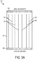
- FIGURES 3A-3D may be understood to represent a portion of a larger backplane arrangement, and that the previously discussed gate electronics and data electronics of FIGURE 2 would be associated with the gate line contacts and the data line contacts.
- bendable flexible substrate 302 associated gate line contacts 304, associated data line contacts 306, and vertical data lines 308.
- the data lines 308 are connected to the data line contacts 306 at the bottom side of the backplane array, as in a conventional layout. It is understood in manufacture, the data lines within the boundaries of the substrate 302 are provided in a layer of metal distinct from the substrate 302, as well as other components including but not limited to the associated gate line contacts 304 and data line contacts 306, of this and other embodiments herein. It is also understood lines 308 are vertical as in the defined vertical direction between the gate line contacts 304 and the data line contacts 306.
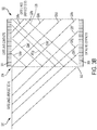
- FIGURE 3B illustrated is a gate line layout 320 according to the present disclosure. Shown again for description purposes is substrate 302, as well as gate line contacts 304, and data line contacts 306, each associated with the substrate 302.
- diagonal (also called non-vertical) gate lines 326a-326h are generated starting from an upper area 322 on the right side of the backplane array (i.e., an area which will include the TFT matrix array, within the boundaries of the substrate) and extending these gate lines to the left side 324 of the array in an upward moving fashion, towards and/or into the gate line contacts 304. It is noted some of the diagonal gate lines 326e-326h (for the purpose of obtaining the layout - but not in actual manufacture) extend past the edge of the substrate 302. As will be seen in FIGURE 3C the gate and data lines cross at all points of the actual rectangular array, showing that this design is capable of providing matrix addressing of every pixel in the array.
- the next step in the layout process is to reflect or fold the layout of the gate lines 326e-326h that protrude to the left side of the substrate of the backplane array, with respect to the left vertical side of the substrate of the backplane array. These are reflected or folded gate lines 326e'-326h'.
- This design procedure ensures that all the pixels can be addressed by the disclosed addressing structure.
- the un-reflected or un-folded gate lines 326a-326d address TFT pixels in the upper right corner of the array (i.e., from gate line 326d to the upper right hand corner of the backplane array.
- the reflected gate lines 326e'-326g' address the TFT pixels in that portion of the backplane array correlating to those gate lines. If the substrate or array is designed to be taller than it is wide, the reflected gate lines leading to the bottom left corner do not intersect the gate line contacts within the array contact area. Instead, gate line 328 is reflected or folded for the right side (marked reflected B), and this line addresses the TFT pixels in the bottom left.
- the gate lines within the boundaries of the substrate 302 are provided in two separate layers of metal distinct from the substrate 302.
- the crossing gate lines is manufactured in one metal layer and the other crossing gate line is manufactured in a second metal layer.
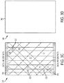
- FIGURE 3C illustrates the resulting layout of the data address lines of FIGURE 3A and the gate address lines of FIGURE 3B combined (i.e., the metal layer carrying the data lines, and the two metal layers each carrying portions of the gate lines which do not crossover other gate lines with in the same metal layer).
- a plurality of TFT/photodiode configurations 332 which in construction, are selectively connected to appropriately corresponding data lines and gate lines (connection lines there between not shown). It is understood such connection lines are not depicted for clarity of viewing, similarly only a sample of the TFT/photodiode configurations 332 are provided for illustration, and it is understood in manufacture further configurations 332 would be provided.
- the configurations 332 are understood to further represent other arrangements such as, but not limited to, those that may be used in construction of display backplanes.
- FIGURE 3D illustrates an insulation layer 340 made of an insulating material 342, and is intended to represent the insulation required for the backplane construction according to the present embodiment.
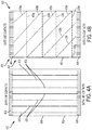
- FIGURES 4A-4D illustrated is a modification of the foregoing design made by translating extra gate lines rather than reflecting or folding them.
- FIGURE 4A depicts the layout for data lines;
- FIGURE 4B depicts the layout for gate lines;
- FIGURE 4C depicts a backplane 430 with the address layers combined (gate and data); and
- FIGURE 4D depicts an insulator layer, and represents the one or more insulator layers of the embodiment.
- bendable flexible substrate 402 gate line contacts 404, data line contacts 406, and vertical data lines 408.
- the data lines 408 are connected to the data line contacts 406 at the bottom side of the backplane array, as in a conventional layout. It is understood in manufacture, the data lines within the boundaries of the substrate 402 are provided in a layer of metal distinct from the substrate 402.
- FIGURE 4B illustrated is a description of the gate lines layout 420. Shown again for description purposes is substrate 402, gate line contacts 404, and data line contacts 406.
- diagonal (also called non-vertical) gate lines 426a-426g are generated starting from an upper area 422 on the right side of the array (e.g., a TFT array area within the boundaries of the substrate) and extending these gate lines 926a-926g to the left 424 of the array in an upward moving fashion (e.g., towards the top of the drawing page where the gate line contacts 404 are located).
- FIGURE 4C illustrates the described data lines layout and gate lines layout combined 430.
- TFT/photodiode configurations 432 which in manufacture are selectively connected to appropriately corresponding data line and gate lines (connection lines there between not shown). It is understood such connection lines are not depicted for clarity of viewing, similarly only a sample of the TFT/photodiode configurations 432 are provided for illustration, and it is understood in manufacture operations further configurations 432 would be provided. Also, the configurations 432 are understood to further represent other arrangements such as, but not limited to, those that may be used in construction of display backplanes.
- FIGURE 4D illustrates an insulation layer 440 made of an insulating material 442, and is intended to represent the insulation required for the backplane construction according to the present embodiment.
- two separate layers of insulation More particularly there would be one insulation layer between the metal layer carrying the data lines, and one of the two metal layers carrying some of the gate address lines, and a second insulation layer between each of the two metal layers carrying portions of the separate gate address lines. Therefore it is understood that the appropriate number and placement of the insulating layers would be included in a backplane such as shown in FIGURE 4C . Also, it is understood that in manufacture via openings would be made in this insulating layer to connect gate or data lines to the TFT/photodiodes, and such vias are not depicted for clarity of viewing.
- FIGURE 3A-3D or 4A-4D have gate lines that cross each other and also cross the data lines.
- the conventional TFT fabrication process has two metal layers that form the matrix addressing, however this is not enough to immediately allow the manufacture the configurations shown in FIGURES 3C and 4C due for example, to the crossing of the gate lines.
- One solution as discussed is to add an additional, third, metal layer, which adds processing complexity.
- Another solution is to include a pair of vias in each pixel, as needed, to allow lines designed in the same metal layer to cross each other using the first and second metal layers. For example, two gate lines that need to cross each other could use a pair of vias to route through the data line layer. It is understood that the opposite could also be done and a data line crossing could be routed through the gate line layer.
- having many vias along an address line may be a problem because it can increase the line resistance and if a single via fails then there will be a defective line.
- the intersection of the gate and data lines shown in FIGURES 3C and 4C is not a square (or a rectangle) as in the conventional TFT backplane geometry.
- the pixel, as defined by the photodiode can remain square or rectangular.
- the photodiode is fabricated in layers above the address lines and its edges do not have to follow the direction of the address lines.
- the horizontally running address lines can be routed around the edges of the square photodiode and so will have a zig-zag shape to form the diagonal gate lines.
- FIGURES 3C and 4C has gate lines going diagonally in both directions from the gate contacts and the total number of gate lines is larger than the number of pixels in a vertical column of pixels.
- a pair of gate lines going in the two directions can be connected to the same gate contact.
- the design selects one or other to address the pixel. Hence it is not necessary to have more gate contacts than in the normal configuration. However it may be a design choice to address the pair of gate lines separately.
- FIGURES 5A-5D illustrate an addressing design that has both the gate and data lines drawn diagonally (also called non-vertical), structured in a similar manner as disclosed in FIGURE 3B , to be able to address all the pixels, i.e., the use of reflecting or folding as discussed in connection with that figure.
- FIGURE 5A depicts the layout for data lines
- FIGURE 5B depicts the layout for gate lines
- FIGURE 5C depicts a backplane with the layers combined
- FIGURE 5D depicts an insulator layer for use in the present embodiment.
- the configuration 500 of FIGURE 5A illustrates substrate 502, gate line contacts 504, and data line contacts 506.
- the process of generating data lines includes generating data lines 508a-508h starting from the right side bottom 507 and moving in a downward direction towards the data line contacts 506 (as opposed to starting from the top and moving towards the gate line contacts in FIGURE 3B ) with data lines 508a-508d in contact with the data line contacts 506.
- FIGURE 5B illustrated is a description of the gate lines layout 520. Shown again for description purposes is substrate 502, gate line contacts 504, and data line contacts 506. Similar actions to those taken in FIGURE 3B are undertaken in FIGURE 5B to obtain gate line 512a-512h and gate lines 512e'-512h', where data lines 512a-512h are generated from the right side toward the left and data lines 512-e'-512h' are continued by reflecting or folding them from the side edges. Further, gate line 514 is formed in the same manner as described in FIGURE 3B for gate line 328.
- FIGURE 5C which also shows exemplary TFT/photodiode arrangements 532).
- configurations 532 are understood to further represent other arrangements such as, but not limited to, those that may be used in construction of display backplanes.
- the angle of the diagonal address lines is in the range of 40 to 50 degrees, including at times approximately 45 degrees.
- Backplane configuration 530 can be easily fabricated with two metal layers, requiring only a single insulation layer, such as layer 540, of an insulating material 542 (as shown in FIGURE 5D ).
- FIGURE 5A selected data lines of FIGURE 5A are manufactured in a first metal layer with the other data lines of FIGURE 5A located in a second metal layer.
- appropriate gate lines of FIGURE 5B are also manufactured in the first metal layer, along with the mentioned data lines.
- the other gate lines of FIGURE 5B are manufactured in the second metal layer, along with the previously mentioned other data lines. Therefore FIGURE 5C can be interpreted to have the illustrated data lines and gate lines provided in the mentioned two metal layers.
- FIGURE 5E This design is further illustrated in FIGURE 5E where selected gate lines A and data lines B (e.g., from FIGURE 5C ) are shown running in parallel and are within a Metal Layer 1, and selected data lines A and gate lines B (e.g., from FIGURE 5C ) are shown running in parallel are within a Metal Layer 2. These metal layers being isolated from each other by an insulation layer as previously discussed.
- This design uses vias near the edge of the array, so for example if the gate lines A in FIGURE 5E are in metal layer 1, then the gate lines B are in metal layer 2, so by use of the vias required interconnections are made. Similar designs may be used for the metal layer separated data lines. This design uses many fewer vias along the address lines than might be used in the embodiments of FIGURES 3C and 4C .
- Each pixel is addressed by one gate and one data line.
- the gate line is in a first metal layer and the data line in another metal layer.
- the metals will be reversed and will require vias within the pixel.
- this is preferable to having vias along the address line because in this case the extra resistance is not a problem and only one pixel is affected if the via process fails.
- the pixel shape for this design can be chosen to be a square (or rectangle) or could be diamond shaped as shown in FIGURE 5E , which also shows that each pixel has both gate and data address lines running in orthogonal directions in the two metal layers.
- the TFT at each pixel is addressed by one or other of the gate and data lines, according to the overall matrix design.
- FIGURE 5E indicates the location of the photodiodes in the pixel.
- the photodiodes are largely fabricated in different layers from the address lines and so can be designed to be on top of at least some of the address lines, so that the area of the pixel forming the photodiode is not significantly reduced.
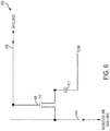
- FIGURE 6 illustrated is a pixel design 600 as may be used in connection with the present disclosure.
- a gate line 602 and data line are provided, where the gate line 602 is connected to the gate a TFT 606, and the data line 604 is connected to the source of the TFT 606.
- the drain of the TFT being connected to a capacitive component 610, with the other end connected to a voltage source Vcom.
- the capacitive component 610 may be a photodiode of other component which may be used as part of a backplane.
- the readout process of selecting one gate line and reading out the data line signals does not immediately give a raster scan of the image. Instead different areas of the array are addressed by one gate line. The image therefore needs to be reconstructed in software based on a knowledge of the addressing design and algorithms to perform this reconstruction are easily developed.
- FIGURE 7 An exemplary bendable flexible detector 700 is depicted in FIGURE 7 .
- a method that may be used to form such a detector includes forming a thin polyimide (PI) layer 702 on a conventional glass substrate. After that processing is complete, a GOS scintillator 704 is bonded to the front surface to give support to the thin PI film and the a-Si layers 706. The combination is then released from a glass substrate and a plastic layer 708 is bonded to the back side for additional protection.
- PI polyimide
- the vertical address lines are defined as the data address lines. It is to be appreciated that in embodiments the gate lines can be made to run in the vertical direction with the data lines in the diagonal or non-vertical direction.
- the same matrix addressing scheme is used for LDC, OLED, or electrophoretic displays and can apply to other pixel array devices.
- the addressing scheme in this disclosure may apply in the same way to these other applications and would enable flexible displays with the same ease of bending because the driver chips are on opposite sides of the array.
- Disclosure has described designs and devices which are made so that the array is bendable.
- the configuration with addressing contacts on opposite ends of the array leaves the two other sides with no contacts.
- the pixels can be fabricated to the edge of the array leaving no dead space along these sides and for some applications the lack of dead space may make this addressing arrangement preferred even if the array is not bent.
Landscapes
- Physics & Mathematics (AREA)
- Nonlinear Science (AREA)
- General Physics & Mathematics (AREA)
- Engineering & Computer Science (AREA)
- Mathematical Physics (AREA)
- Chemical & Material Sciences (AREA)
- Crystallography & Structural Chemistry (AREA)
- Optics & Photonics (AREA)
- Microelectronics & Electronic Packaging (AREA)
- Life Sciences & Earth Sciences (AREA)
- Health & Medical Sciences (AREA)
- High Energy & Nuclear Physics (AREA)
- Molecular Biology (AREA)
- Spectroscopy & Molecular Physics (AREA)
- Computer Hardware Design (AREA)
- Theoretical Computer Science (AREA)
- Solid State Image Pick-Up Elements (AREA)
- Devices For Indicating Variable Information By Combining Individual Elements (AREA)
- Liquid Crystal (AREA)
- Electroluminescent Light Sources (AREA)
- Transforming Light Signals Into Electric Signals (AREA)
- Measurement Of Radiation (AREA)
Abstract
Description
- The present disclosure is directed to electronic backplanes and more particularly to backplanes which employ bendable flexible substrates.
- Backplanes carry electronic components including but not limited to transistors (e.g., thin film transistors (TFTs), etc.) which are addressed via gate lines and data lines.
- Traditionally, backplanes have been fabricated with glass substrates, resulting in rigid backplanes, which limits the areas where they may be employed. Therefore there is the present interest in manufacturing backplanes with bendable flexible (e.g., plastic, polymers, etc.) substrates in order to increase the overall bendability or flexibility of the backplane itself, which expands the areas where they may be used.
- An issue concerning bendable flexible backplanes is however, the electronics used to address the electronic devices of the backplane (e.g., TFTs, etc.). Such electronics include chip-on-flex (COF) packages and/or printed circuit boards (PCBs). These electronics have much less bendability flexibility than the bendable flexible substrate. Therefore, when using common backplane architecture the benefit of the bendable flexible substrate is diminished. Particularly, in such architecture the sets of addressing lines (e.g., data addressing lines and gate addressing lines) run substantially in horizontal and vertical manners crossing each other (though in different metal layers and isolated from each other) at substantially 90 degrees. This arrangement causes the associated addressing electronics (e.g. the chip on flex (COF) packages, PCBs, etc.) to be positioned on adjacent sides of the backplane which acts to restrict the overall flexibility bendability of the backplane.
- The present disclosure is directed to the design and manufacture of backplanes which overcome the existing limitations in order to increase bendability and flexibility.
- A flexible TFT backplane includes, a flexible substrate, a first set of address line contacts associated with the substrate, and a second set of address line contacts associated with the substrate. The first set of address line contacts and the second set of address line contacts are located at opposite sides of the substrate from each other, defining a vertical direction. A first set of address lines designed to run in one of the vertical direction and a diagonal or non-vertical direction with respect to the defined vertical direction, with the first set of address lines connected to the first set of address line contacts. Also provided is a second set of address lines designed to run in one of a diagonal or non-vertical direction with respect to the defined vertical direction, and a combination of diagonal and horizontal directions with respect to the vertical direction, with the second set of address lines connected to the second set of address line contacts. At least one insulating layer is located between the first set of address lines and the second set of address lines, and a plurality of TFTs arranged in an array, within the boundaries of the substrate, wherein the TFTs are addressed by the first set of address lines and the second set of address lines.
-
-
FIGURE 1 illustrates a conventional structure of an active matrix detector TFT backplane with gate drivers and data readout on adjacent sides of the active matrix. -
FIGURE 2 illustrates a backplane structure in accordance with the present disclosure where gate driver devices are on a side of the backplane opposite a side from data readout devices, enabling increased continuous bending or flexing. -
FIGURES 3A-3D illustrate an embodiment of the design and construction of gate and data address lines terminating on the opposite sides of a TFT backplane segment according to the present disclosure. -
FIGURE 4A-4D illustrate an alternative embodiment of the design and construction of a TFT backplane segment according to the present disclosure. -
FIGURES 5A-5D illustrate an alternative embodiment of the design and construction of a TFT backplane segment addressing arrangement with both gate and data lines running diagonally across the array and continuing back when they reach the outer edge of the array. -
FIGURE 5E illustrates a close-up view of the pixel arrangement in regions of the array where there are two gate lines and two data lines near each pixel, where the diamond shapes illustrates the location of the photodiode in each pixel. -
FIGURE 6 illustrates are more detailed view of a pixel arrangement. -
FIGURE 7 illustrates an exemplary bendable detector. - Backplanes which implement an array of electronic devices, such as TFTs, etc. are useful in a wide variety of products and systems. Providing a backplane with increased bendability flexibility further increases the usefulness of such backplanes. In embodiments described herein TFT-type backplanes are disclosed having gate and data addressing contacts (of addressing electronics, including but not limited to COFs and PCBs) positioned on opposite sides of the backplane (as opposed to adjacent to each other) and an arrangement of gate address lines and data address lines designed to address all of the TFT pixels of the array. The disclosed embodiments can be used in a variety of implementations such as for detectors, including x-ray detectors, LCD devices, OLED devices, and reflective displays, among numerous others. Therefore, while the present discussion may describe particular implementations, it should be understood that backplanes with the architectures described herein are not limited thereto.
- For purposes of discussion, the following describes an implementation where a disclosed for use with detectors, such as digital x-ray detectors. These devices can commonly be fabricated on a glass using an amorphous silicon (a-Si) thin film transistor (TFT) backplane and an a-Si photodiode. Other materials can be used, such as but not limited to metal oxides, polycrystalline silicon, and organic semiconductors for the TFT and organic materials for the photodiode. An x-ray scintillator is placed in contact with the backplane to convert x-rays to light that is detected by the photodiode. The scintillator is typically either Tb-doped gadolinium oxysulphide (GOS) or Csl, but other materials are possible. The GOS may be adhesive bonded to the backplane or simply pushed into contact. The Csl may be deposited directly on the backplane or formed as a separate layer pushed into contact. An alternative approach is to use an x-ray photoconductor such as selenium with a very similar TFT backplane. The current disclosure applies to either type of structure, as well as others including manufacture of display devices using known manufacturing processes.
- The same TFT and photodiode structures can be deposited on a plastic substrate instead of glass to form a bendable flexible. There are various known fabrication processes to make a photodiode array addressed by a TFT detector backplane on a flexible substrate. A common method that is used in current manufacturing is to form a thin polyimide (PI) layer on a conventional glass substrate. The TFT backplane is then manufactured with the same process as if it were on glass without the PI layer. After the processing is complete, the GOS scintillator is bonded to the front surface to give support to the thin PI film and the a-Si layers. The combination is then released from the glass substrate and a plastic layer is bonded to the back side for additional protection. The flexible nature of the plastic substrates and GOS scintillator make the array bendable.
- Bendable detectors are of interest, for example to inspect pipelines or other curved objects, to image objects in confined spaces where a rigid flat detector could not be introduced, and to conform to the human body for added comfort and resolution.
- Active matrix designs such as the described digital x-ray detectors, perform addressing by sequentially applying a voltage pulse to the gate lines of the TFTs (also called scan lines) while reading out the charge signal on the data lines.
- Turning to
FIGURE 1 , illustrated is a bendableflexible backplane structure 100 which has a bendableflexible substrate 102, carrying a TFT matrix 104 (which includes a plurality of TFTs and associated gate lines and data lines formed in a conventional manner).Gate lines portions 106, 108 (shown as two single lines for convenience of viewing, as it understood there would be numerous additional ones of these gate line portions of the gate lines) extend from theTFT matrix 104, and contact shift register usually in the form of a silicon integrated circuit (the gate chips) 110, 112, viagate contacts gate chips substrate 102. Similarly,data line portions 118, 120 (again two single lines for viewing convenience) are connected todata readout chips COF packages flexible substrate 102. Thedata COFs PCB 130, but many of the available gate chips do not require a connection to a PCB. - As can be seen from
FIGURE 1 , thegate packages data packages 126, 128 (as well as the PCB 130) are positioned on immediately adjacent sides of the bendableflexible substrate 102. - One-dimensional bending of the
structure 100 is best done with curvature in the gate line direction (see 132 ofFIGURE 1 ) as this does not require bending of thePCB 130. However, thegate chips COF packages rigid gate chips COFs - The proposed solution to the limited bendability flexibility of the
structure 100 ofFIGURE 1 , is to manufacture a backplane design with the gate electronics (e.g., gate drivers such as the gate COFs), and data electronics (e.g., data readout connections such as the data COFs) positioned on opposite sides of the backplane array as illustrated instructure 120 ofFIGURE 2 , rather than at immediately adjacent sides as shown inFIGURE 1 . However, this configuration is not possible with the conventional arrangement of gate and data address lines (i.e., in horizontal versus vertical, causing a 90 degree crossing of the gate and data address lines). Therefore this disclosure describes architectures that are able to address the array of TFTs in a manner that increases bendability and flexibility. It is mentioned that for convenience theTFT matrix 104a ofFIGURE 2 may appears to depict addressing lines in a conventional manner, however it is understood theTFT matrix 104a is intended to include address line arrangements as disclosed herein which permit the placement of the gate electronics and data electronics as shown inFIGURE 2 . - Turning to
FIGURES 3A-3D depicted are stages of a backplane architecture which allows for the placement of gate line contacts and data line contacts on opposite sides of a bendable flexible substrate carrying a transistor (TFT) array.FIGURE 3A depicts the layout for data lines;FIGURE 3B depicts the layout for gate lines;FIGURE 3C depicts a backplane with the layers combined; andFIGURE 3D depicts an insulator layer, and represents the one or more insulator layers of the embodiment. - Placement of the gate line contacts and data line contacts on opposite sides of a bendable flexible substrate is achieved by employing unique design layout of the addressing lines (i.e., data lines and gate lines) on the bendable flexible backplane. It is to be appreciated
FIGURES 3A-3D may be understood to represent a portion of a larger backplane arrangement, and that the previously discussed gate electronics and data electronics ofFIGURE 2 would be associated with the gate line contacts and the data line contacts. - Returning to
configuration 300 ofFIGURE 3A , illustrated is bendableflexible substrate 302, associatedgate line contacts 304, associateddata line contacts 306, and vertical data lines 308. The data lines 308 are connected to thedata line contacts 306 at the bottom side of the backplane array, as in a conventional layout. It is understood in manufacture, the data lines within the boundaries of thesubstrate 302 are provided in a layer of metal distinct from thesubstrate 302, as well as other components including but not limited to the associatedgate line contacts 304 anddata line contacts 306, of this and other embodiments herein. It is also understoodlines 308 are vertical as in the defined vertical direction between thegate line contacts 304 and thedata line contacts 306. - Turning now to
FIGURE 3B illustrated is agate line layout 320 according to the present disclosure. Shown again for description purposes issubstrate 302, as well asgate line contacts 304, anddata line contacts 306, each associated with thesubstrate 302. - Initially, diagonal (also called non-vertical)
gate lines 326a-326h (with respect to the defined vertical direction) are generated starting from anupper area 322 on the right side of the backplane array (i.e., an area which will include the TFT matrix array, within the boundaries of the substrate) and extending these gate lines to theleft side 324 of the array in an upward moving fashion, towards and/or into thegate line contacts 304. It is noted some of thediagonal gate lines 326e-326h (for the purpose of obtaining the layout - but not in actual manufacture) extend past the edge of thesubstrate 302. As will be seen inFIGURE 3C the gate and data lines cross at all points of the actual rectangular array, showing that this design is capable of providing matrix addressing of every pixel in the array. - The next step in the layout process is to reflect or fold the layout of the
gate lines 326e-326h that protrude to the left side of the substrate of the backplane array, with respect to the left vertical side of the substrate of the backplane array. These are reflected or foldedgate lines 326e'-326h'. This means that thegate lines 326e'-326h' are drawn as connected to and going diagonally down from thegate line contacts 304 to the left, and when the gate line reaches the edge of the array the gate line continues in a diagonal going down to the right (i.e., those portions of 326e-326h that are within the boundaries of the substrate of the backplane array. This design procedure ensures that all the pixels can be addressed by the disclosed addressing structure. - It can be seen that the un-reflected or
un-folded gate lines 326a-326d address TFT pixels in the upper right corner of the array (i.e., fromgate line 326d to the upper right hand corner of the backplane array. The reflectedgate lines 326e'-326g' address the TFT pixels in that portion of the backplane array correlating to those gate lines. If the substrate or array is designed to be taller than it is wide, the reflected gate lines leading to the bottom left corner do not intersect the gate line contacts within the array contact area. Instead,gate line 328 is reflected or folded for the right side (marked reflected B), and this line addresses the TFT pixels in the bottom left. - It is understood in manufacture, the gate lines within the boundaries of the
substrate 302 are provided in two separate layers of metal distinct from thesubstrate 302. In particular, wherever gate lines in the layout ofFIGURE 3B cross each other, in order to avoid a shorting situation, one of the crossing gate lines is manufactured in one metal layer and the other crossing gate line is manufactured in a second metal layer. -
FIGURE 3C illustrates the resulting layout of the data address lines ofFIGURE 3A and the gate address lines ofFIGURE 3B combined (i.e., the metal layer carrying the data lines, and the two metal layers each carrying portions of the gate lines which do not crossover other gate lines with in the same metal layer). Also depicted are a plurality of TFT/photodiode configurations 332, which in construction, are selectively connected to appropriately corresponding data lines and gate lines (connection lines there between not shown). It is understood such connection lines are not depicted for clarity of viewing, similarly only a sample of the TFT/photodiode configurations 332 are provided for illustration, and it is understood in manufacturefurther configurations 332 would be provided. Also, theconfigurations 332 are understood to further represent other arrangements such as, but not limited to, those that may be used in construction of display backplanes. -
FIGURE 3D illustrates aninsulation layer 340 made of an insulatingmaterial 342, and is intended to represent the insulation required for the backplane construction according to the present embodiment. In this embodiment, there are two separate layers of insulation. More particularly there would be one insulation layer between the metal layer carrying the data lines, and one of the two metal layers carrying some of the gate address lines, and a second insulation layer between each of the two metal layers carrying portions of the separate gate address lines. Therefore it is understood that the appropriate number and placement of the insulating layers would be included in a backplane such as shown inFIGURE 3C . Also, it is understood that in manufacture via openings would be made in this insulating layer to connect gate or data lines to the TFT/photodiodes, and such vias are not depicted for clarity of viewing. - Turning now to
FIGURES 4A-4D , illustrated is a modification of the foregoing design made by translating extra gate lines rather than reflecting or folding them.FIGURE 4A depicts the layout for data lines;FIGURE 4B depicts the layout for gate lines;FIGURE 4C depicts abackplane 430 with the address layers combined (gate and data); andFIGURE 4D depicts an insulator layer, and represents the one or more insulator layers of the embodiment. - Returning to the
configuration 400 ofFIGURE 4A , illustrated is bendableflexible substrate 402,gate line contacts 404,data line contacts 406, and vertical data lines 408. The data lines 408 are connected to thedata line contacts 406 at the bottom side of the backplane array, as in a conventional layout. It is understood in manufacture, the data lines within the boundaries of thesubstrate 402 are provided in a layer of metal distinct from thesubstrate 402. - Turning now to
FIGURE 4B illustrated is a description of thegate lines layout 420. Shown again for description purposes issubstrate 402,gate line contacts 404, anddata line contacts 406. - Initially, in this embodiment, diagonal (also called non-vertical)
gate lines 426a-426g are generated starting from anupper area 422 on the right side of the array (e.g., a TFT array area within the boundaries of the substrate) and extending these gate lines 926a-926g to the left 424 of the array in an upward moving fashion (e.g., towards the top of the drawing page where thegate line contacts 404 are located). In this case there is provided (instead of the reflected or folded lines) connectinghorizontal lines 428a-428d.FIGURE 4C illustrates the described data lines layout and gate lines layout combined 430. Also depicted are a plurality of TFT/photodiode configurations 432, which in manufacture are selectively connected to appropriately corresponding data line and gate lines (connection lines there between not shown). It is understood such connection lines are not depicted for clarity of viewing, similarly only a sample of the TFT/photodiode configurations 432 are provided for illustration, and it is understood in manufacture operationsfurther configurations 432 would be provided. Also, theconfigurations 432 are understood to further represent other arrangements such as, but not limited to, those that may be used in construction of display backplanes. -
FIGURE 4D illustrates aninsulation layer 440 made of an insulatingmaterial 442, and is intended to represent the insulation required for the backplane construction according to the present embodiment. In this embodiment two separate layers of insulation. More particularly there would be one insulation layer between the metal layer carrying the data lines, and one of the two metal layers carrying some of the gate address lines, and a second insulation layer between each of the two metal layers carrying portions of the separate gate address lines. Therefore it is understood that the appropriate number and placement of the insulating layers would be included in a backplane such as shown inFIGURE 4C . Also, it is understood that in manufacture via openings would be made in this insulating layer to connect gate or data lines to the TFT/photodiodes, and such vias are not depicted for clarity of viewing. - As discussed it has been noted the designs of
FIGURE 3A-3D or4A-4D have gate lines that cross each other and also cross the data lines. The conventional TFT fabrication process has two metal layers that form the matrix addressing, however this is not enough to immediately allow the manufacture the configurations shown inFIGURES 3C and4C due for example, to the crossing of the gate lines. - One solution as discussed is to add an additional, third, metal layer, which adds processing complexity. Another solution is to include a pair of vias in each pixel, as needed, to allow lines designed in the same metal layer to cross each other using the first and second metal layers. For example, two gate lines that need to cross each other could use a pair of vias to route through the data line layer. It is understood that the opposite could also be done and a data line crossing could be routed through the gate line layer. However, having many vias along an address line may be a problem because it can increase the line resistance and if a single via fails then there will be a defective line.
- The intersection of the gate and data lines shown in
FIGURES 3C and4C is not a square (or a rectangle) as in the conventional TFT backplane geometry. However, the pixel, as defined by the photodiode can remain square or rectangular. The photodiode is fabricated in layers above the address lines and its edges do not have to follow the direction of the address lines. Alternatively the horizontally running address lines can be routed around the edges of the square photodiode and so will have a zig-zag shape to form the diagonal gate lines. - The design of
FIGURES 3C and4C has gate lines going diagonally in both directions from the gate contacts and the total number of gate lines is larger than the number of pixels in a vertical column of pixels. However, a pair of gate lines going in the two directions can be connected to the same gate contact. Where two gate lines cross at a pixel, the design selects one or other to address the pixel. Hence it is not necessary to have more gate contacts than in the normal configuration. However it may be a design choice to address the pair of gate lines separately. -
FIGURES 5A-5D illustrate an addressing design that has both the gate and data lines drawn diagonally (also called non-vertical), structured in a similar manner as disclosed inFIGURE 3B , to be able to address all the pixels, i.e., the use of reflecting or folding as discussed in connection with that figure. -
FIGURE 5A depicts the layout for data lines;FIGURE 5B depicts the layout for gate lines;FIGURE 5C depicts a backplane with the layers combined; andFIGURE 5D depicts an insulator layer for use in the present embodiment. - The
configuration 500 ofFIGURE 5A illustratessubstrate 502,gate line contacts 504, anddata line contacts 506. In an embodiment, the process of generating data lines includes generatingdata lines 508a-508h starting from theright side bottom 507 and moving in a downward direction towards the data line contacts 506 (as opposed to starting from the top and moving towards the gate line contacts inFIGURE 3B ) withdata lines 508a-508d in contact with thedata line contacts 506. As understood from the discussion inFIGURE 3B , ones of thedata lines 508a-508h ofFIGURE 5 , which would protrude past the substrate 502 (in thisembodiment data lines 508e'-508h' (the protruding is not shown in this figure).Further data line 510 is formed in a similar manner as described inFIGURE 3B forgate line 328. - Turning to
FIGURE 5B illustrated is a description of thegate lines layout 520. Shown again for description purposes issubstrate 502,gate line contacts 504, anddata line contacts 506. Similar actions to those taken inFIGURE 3B are undertaken inFIGURE 5B to obtaingate line 512a-512h andgate lines 512e'-512h', wheredata lines 512a-512h are generated from the right side toward the left and data lines 512-e'-512h' are continued by reflecting or folding them from the side edges. Further,gate line 514 is formed in the same manner as described inFIGURE 3B forgate line 328. - An advantage of this scheme is that all the lines run diagonally either to the left or the right, as shown in
configuration 530 ofFIGURE 5C (which also shows exemplary TFT/photodiode arrangements 532). Also, theconfigurations 532 are understood to further represent other arrangements such as, but not limited to, those that may be used in construction of display backplanes. - In this and the other embodiments disclosed herein, the angle of the diagonal address lines is in the range of 40 to 50 degrees, including at times approximately 45 degrees.
-
Backplane configuration 530 can be easily fabricated with two metal layers, requiring only a single insulation layer, such aslayer 540, of an insulating material 542 (as shown inFIGURE 5D ). - For example, selected data lines of
FIGURE 5A are manufactured in a first metal layer with the other data lines ofFIGURE 5A located in a second metal layer. Further, appropriate gate lines ofFIGURE 5B are also manufactured in the first metal layer, along with the mentioned data lines. Similarly the other gate lines ofFIGURE 5B are manufactured in the second metal layer, along with the previously mentioned other data lines. ThereforeFIGURE 5C can be interpreted to have the illustrated data lines and gate lines provided in the mentioned two metal layers. - This design is further illustrated in
FIGURE 5E where selected gate lines A and data lines B (e.g., fromFIGURE 5C ) are shown running in parallel and are within aMetal Layer 1, and selected data lines A and gate lines B (e.g., fromFIGURE 5C ) are shown running in parallel are within aMetal Layer 2. These metal layers being isolated from each other by an insulation layer as previously discussed. This design uses vias near the edge of the array, so for example if the gate lines A inFIGURE 5E are inmetal layer 1, then the gate lines B are inmetal layer 2, so by use of the vias required interconnections are made. Similar designs may be used for the metal layer separated data lines. This design uses many fewer vias along the address lines than might be used in the embodiments ofFIGURES 3C and4C . - Each pixel is addressed by one gate and one data line. In the conventional backplane the gate line is in a first metal layer and the data line in another metal layer. In some of the pixels of this design the metals will be reversed and will require vias within the pixel. However, this is preferable to having vias along the address line because in this case the extra resistance is not a problem and only one pixel is affected if the via process fails.
- The pixel shape for this design can be chosen to be a square (or rectangle) or could be diamond shaped as shown in
FIGURE 5E , which also shows that each pixel has both gate and data address lines running in orthogonal directions in the two metal layers. The TFT at each pixel is addressed by one or other of the gate and data lines, according to the overall matrix design. - Having twice as many address lines as some other conventional configuration does not cause degradation in the imager or other device performance.
FIGURE 5E indicates the location of the photodiodes in the pixel. However, the photodiodes are largely fabricated in different layers from the address lines and so can be designed to be on top of at least some of the address lines, so that the area of the pixel forming the photodiode is not significantly reduced. There are designs in which the photodiode completely covers the pixel. - Turning to
FIGURE 6 illustrated is apixel design 600 as may be used in connection with the present disclosure. As shown, agate line 602 and data line are provided, where thegate line 602 is connected to the gate aTFT 606, and thedata line 604 is connected to the source of theTFT 606. The drain of the TFT being connected to acapacitive component 610, with the other end connected to a voltage source Vcom. Thecapacitive component 610 may be a photodiode of other component which may be used as part of a backplane. - Because of the arrangement of gate and data lines, the readout process of selecting one gate line and reading out the data line signals, does not immediately give a raster scan of the image. Instead different areas of the array are addressed by one gate line. The image therefore needs to be reconstructed in software based on a knowledge of the addressing design and algorithms to perform this reconstruction are easily developed.
- The present disclosure has been described in the context of a TFT backplane for an x-ray imager. An exemplary bendable
flexible detector 700 is depicted inFIGURE 7 . A method that may be used to form such a detector includes forming a thin polyimide (PI)layer 702 on a conventional glass substrate. After that processing is complete, aGOS scintillator 704 is bonded to the front surface to give support to the thin PI film and the a-Si layers 706. The combination is then released from a glass substrate and aplastic layer 708 is bonded to the back side for additional protection. - It has been described herein as the vertical address lines are defined as the data address lines. It is to be appreciated that in embodiments the gate lines can be made to run in the vertical direction with the data lines in the diagonal or non-vertical direction.
- The same matrix addressing scheme is used for LDC, OLED, or electrophoretic displays and can apply to other pixel array devices. The addressing scheme in this disclosure may apply in the same way to these other applications and would enable flexible displays with the same ease of bending because the driver chips are on opposite sides of the array.
- Disclosure has described designs and devices which are made so that the array is bendable. The configuration with addressing contacts on opposite ends of the array leaves the two other sides with no contacts. The pixels can be fabricated to the edge of the array leaving no dead space along these sides and for some applications the lack of dead space may make this addressing arrangement preferred even if the array is not bent.
- It will be appreciated that variants of the above-disclosed and other features and functions, or alternatives thereof, may be combined into many other different systems or applications. Various presently unforeseen or unanticipated alternatives, modifications, variations or improvements therein may be subsequently made by those skilled in the art which are also intended to be encompassed by the following claims.
Claims (10)
- A flexible TFT backplane comprising:a flexible substrate;a first set of address line contacts associated with the substrate;a second set of address line contacts associated with the substrate, the first set of address line contacts and the second set of address line contacts located at opposite sides of the substrate from each other, defining a vertical direction;a first set of address lines designed to run in one of the defined vertical direction, and a diagonal direction with respect to the defined vertical direction, the first set of address lines connected to the first set of address line contacts;a second set of address lines designed to run in one of a diagonal direction with respect to the defined vertical direction and a combination of diagonal and horizontal directions with respect to the vertical direction, the second set of address lines connected to the second set of address line contacts;at least one insulating layer located between the first set of address lines and the second set of address lines; anda plurality of TFTs arranged in an array within boundaries of the substrate, wherein the TFTs are addressed by the first set of address lines and the second set of address lines.
- The flexible TFT backplane according to claim 1 further including components to form a digital x-ray detector.
- The flexible TFT backplane according to claim 1 wherein the first set of address line contacts are data line contacts and the second set of address line contacts gate line contacts.
- The flexible TFT backplane according to claim 3 wherein the first set of address lines are a set of data lines and the second set of address lines are a set of gate lines.
- The flexible TFT backplane according to claim 4 wherein the set of data lines run in the diagonal direction.
- The flexible TFT backplane according to claim 4 wherein the set of data lines run in the vertical direction.
- The flexible TFT backplane according to claim 1 wherein the arrangement of address lines address all pixels of the TFT array.
- A method of forming a flexible TFT backplane comprising:providing a flexible substrate;forming a first set of address line contacts associated with the substrate;forming a second set of address line contacts associated with the substrate, the first set of address line contacts and the second set of address line contacts located at opposite sides of the substrate from each other, defining a vertical direction;forming a first set of address lines designed to run in one of the defined vertical direction, and a diagonal direction with respect to the defined vertical direction, the first set of address lines connected to the first set of address line contacts;forming a second set of address lines designed to run in one of a diagonal direction with respect to the defined vertical direction and a combination of diagonal and horizontal directions with respect to the defined vertical direction, the second set of address lines connected to the second set of address line contacts;forming at least one insulating layer located between the first set of address lines and the second set of address lines; andproviding a plurality of TFTs arranged in an array within boundaries of the substrate, wherein the TFTs are addressed by the first set of address lines and the second set of address lines.
- The method according to claim 8 wherein the first set of address line contacts are data line contacts and the second set of address line contacts gate line contacts.
- The method according to claim 9 wherein the first set of address lines are a set of data lines and the second set of address lines are a set of gate lines.
Applications Claiming Priority (1)
| Application Number | Priority Date | Filing Date | Title |
|---|---|---|---|
| US15/845,058 US10197831B1 (en) | 2017-12-18 | 2017-12-18 | Bendable TFT backplane with addressing contacts at opposite ends |
Publications (1)
| Publication Number | Publication Date |
|---|---|
| EP3499572A1 true EP3499572A1 (en) | 2019-06-19 |
Family
ID=64949029
Family Applications (1)
| Application Number | Title | Priority Date | Filing Date |
|---|---|---|---|
| EP18212113.7A Withdrawn EP3499572A1 (en) | 2017-12-18 | 2018-12-12 | Bendable tft backplane with addressing contacts at opposite ends |
Country Status (4)
| Country | Link |
|---|---|
| US (1) | US10197831B1 (en) |
| EP (1) | EP3499572A1 (en) |
| JP (1) | JP7161383B2 (en) |
| CN (1) | CN109935598A (en) |
Families Citing this family (2)
| Publication number | Priority date | Publication date | Assignee | Title |
|---|---|---|---|---|
| JP7070508B2 (en) | 2019-06-13 | 2022-05-18 | いすゞ自動車株式会社 | Inspection support program and inspection support system |
| US11842667B2 (en) * | 2021-10-27 | 2023-12-12 | New Vision Display, Inc. | Diagonal addressing of electronic displays |
Citations (9)
| Publication number | Priority date | Publication date | Assignee | Title |
|---|---|---|---|---|
| US20030031296A1 (en) * | 2001-07-27 | 2003-02-13 | Martin Hoheisel | X-ray diagnostics installation with a flexible solid state X-ray detector |
| WO2004063803A1 (en) * | 2003-01-15 | 2004-07-29 | Philips Intellectual Property & Standards Gmbh | Device comprising an array of electronic elements, based on diagonal line routing |
| US20080011960A1 (en) * | 2006-07-14 | 2008-01-17 | Eastman Kodak Company | Apparatus for asymmetric dual-screen digital radiography |
| WO2010070735A1 (en) * | 2008-12-16 | 2010-06-24 | 株式会社島津製作所 | Optical matrix device |
| EP2919224A1 (en) * | 2014-03-13 | 2015-09-16 | Samsung Display Co., Ltd. | Display apparatus and method of driving the same |
| WO2015196683A1 (en) * | 2014-06-27 | 2015-12-30 | 京东方科技集团股份有限公司 | Array substrate and drive method therefor, flexible display device and electronic apparatus |
| US20160035298A1 (en) * | 2013-09-04 | 2016-02-04 | Boe Technology Group Co., Ltd. | Array substrate, method for driving the same, flexible display device and electronic equipment |
| US20160307528A1 (en) * | 2014-04-02 | 2016-10-20 | Boe Technology Group Co., Ltd. | Array substrate, flexible display device and electronic device |
| CN106125429A (en) * | 2016-08-23 | 2016-11-16 | 深圳市华星光电技术有限公司 | Display panels and liquid crystal indicator |
Family Cites Families (2)
| Publication number | Priority date | Publication date | Assignee | Title |
|---|---|---|---|---|
| WO2005107235A1 (en) * | 2004-05-05 | 2005-11-10 | Koninklijke Philips Electronics N.V. | Electronic device with an array of processing units |
| KR102161810B1 (en) | 2014-10-27 | 2020-10-07 | 삼성디스플레이 주식회사 | Display device |
-
2017
- 2017-12-18 US US15/845,058 patent/US10197831B1/en active Active
-
2018
- 2018-11-22 JP JP2018218963A patent/JP7161383B2/en active Active
- 2018-12-03 CN CN201811464619.2A patent/CN109935598A/en active Pending
- 2018-12-12 EP EP18212113.7A patent/EP3499572A1/en not_active Withdrawn
Patent Citations (9)
| Publication number | Priority date | Publication date | Assignee | Title |
|---|---|---|---|---|
| US20030031296A1 (en) * | 2001-07-27 | 2003-02-13 | Martin Hoheisel | X-ray diagnostics installation with a flexible solid state X-ray detector |
| WO2004063803A1 (en) * | 2003-01-15 | 2004-07-29 | Philips Intellectual Property & Standards Gmbh | Device comprising an array of electronic elements, based on diagonal line routing |
| US20080011960A1 (en) * | 2006-07-14 | 2008-01-17 | Eastman Kodak Company | Apparatus for asymmetric dual-screen digital radiography |
| WO2010070735A1 (en) * | 2008-12-16 | 2010-06-24 | 株式会社島津製作所 | Optical matrix device |
| US20160035298A1 (en) * | 2013-09-04 | 2016-02-04 | Boe Technology Group Co., Ltd. | Array substrate, method for driving the same, flexible display device and electronic equipment |
| EP2919224A1 (en) * | 2014-03-13 | 2015-09-16 | Samsung Display Co., Ltd. | Display apparatus and method of driving the same |
| US20160307528A1 (en) * | 2014-04-02 | 2016-10-20 | Boe Technology Group Co., Ltd. | Array substrate, flexible display device and electronic device |
| WO2015196683A1 (en) * | 2014-06-27 | 2015-12-30 | 京东方科技集团股份有限公司 | Array substrate and drive method therefor, flexible display device and electronic apparatus |
| CN106125429A (en) * | 2016-08-23 | 2016-11-16 | 深圳市华星光电技术有限公司 | Display panels and liquid crystal indicator |
Also Published As
| Publication number | Publication date |
|---|---|
| CN109935598A (en) | 2019-06-25 |
| JP7161383B2 (en) | 2022-10-26 |
| JP2019110526A (en) | 2019-07-04 |
| US10197831B1 (en) | 2019-02-05 |
Similar Documents
| Publication | Publication Date | Title |
|---|---|---|
| US12314503B2 (en) | Display device with sensor | |
| CN110911444B (en) | Display device | |
| US12105566B2 (en) | Display device | |
| US9291843B2 (en) | Display apparatus | |
| CN110931523B (en) | Display device | |
| CN113540120A (en) | Display device | |
| US12210790B2 (en) | Electronic device | |
| JP2018066933A (en) | Display | |
| CN111142295A (en) | Display device | |
| CN112071206B (en) | Display panel and display device | |
| JP2014149429A (en) | Liquid crystal display device and method for manufacturing liquid crystal display device | |
| US10930677B2 (en) | Alternative designs for addressing contacts that enhance bend ability of TFT backplanes | |
| KR101750431B1 (en) | Thin film transistor array panel | |
| US10197831B1 (en) | Bendable TFT backplane with addressing contacts at opposite ends | |
| CN101071214A (en) | Liquid crystal display and manufacturing method thereof | |
| JP2019124787A (en) | Display device and electronic shelf label | |
| KR20210079431A (en) | Display module and method for manufacturing display device | |
| EP4206810B1 (en) | Array substrate and display device | |
| JP2005268282A (en) | Semiconductor chip package and display device using the same | |
| JP6652901B2 (en) | Display device and method of manufacturing the same | |
| CN107390440B (en) | Display device | |
| US20170322464A1 (en) | Liquid-crystal display device | |
| JP5034434B2 (en) | Electro-optic device | |
| JP2004219712A (en) | Wiring structure for display panel | |
| CN122054792A (en) | Display panel and display device |
Legal Events
| Date | Code | Title | Description |
|---|---|---|---|
| PUAI | Public reference made under article 153(3) epc to a published international application that has entered the european phase |
Free format text: ORIGINAL CODE: 0009012 |
|
| STAA | Information on the status of an ep patent application or granted ep patent |
Free format text: STATUS: THE APPLICATION HAS BEEN PUBLISHED |
|
| AK | Designated contracting states |
Kind code of ref document: A1 Designated state(s): AL AT BE BG CH CY CZ DE DK EE ES FI FR GB GR HR HU IE IS IT LI LT LU LV MC MK MT NL NO PL PT RO RS SE SI SK SM TR |
|
| AX | Request for extension of the european patent |
Extension state: BA ME |
|
| STAA | Information on the status of an ep patent application or granted ep patent |
Free format text: STATUS: REQUEST FOR EXAMINATION WAS MADE |
|
| 17P | Request for examination filed |
Effective date: 20191219 |
|
| RBV | Designated contracting states (corrected) |
Designated state(s): AL AT BE BG CH CY CZ DE DK EE ES FI FR GB GR HR HU IE IS IT LI LT LU LV MC MK MT NL NO PL PT RO RS SE SI SK SM TR |
|
| STAA | Information on the status of an ep patent application or granted ep patent |
Free format text: STATUS: EXAMINATION IS IN PROGRESS |
|
| 17Q | First examination report despatched |
Effective date: 20211022 |
|
| STAA | Information on the status of an ep patent application or granted ep patent |
Free format text: STATUS: THE APPLICATION IS DEEMED TO BE WITHDRAWN |
|
| 18D | Application deemed to be withdrawn |
Effective date: 20231107 |