EP3496156A1 - Solar cell - Google Patents
Solar cell Download PDFInfo
- Publication number
- EP3496156A1 EP3496156A1 EP18183100.9A EP18183100A EP3496156A1 EP 3496156 A1 EP3496156 A1 EP 3496156A1 EP 18183100 A EP18183100 A EP 18183100A EP 3496156 A1 EP3496156 A1 EP 3496156A1
- Authority
- EP
- European Patent Office
- Prior art keywords
- solar cell
- glass
- glass frits
- glass frit
- frits
- Prior art date
- Legal status (The legal status is an assumption and is not a legal conclusion. Google has not performed a legal analysis and makes no representation as to the accuracy of the status listed.)
- Granted
Links
Images


Classifications
-
- H—ELECTRICITY
- H10—SEMICONDUCTOR DEVICES; ELECTRIC SOLID-STATE DEVICES NOT OTHERWISE PROVIDED FOR
- H10F—INORGANIC SEMICONDUCTOR DEVICES SENSITIVE TO INFRARED RADIATION, LIGHT, ELECTROMAGNETIC RADIATION OF SHORTER WAVELENGTH OR CORPUSCULAR RADIATION
- H10F19/00—Integrated devices, or assemblies of multiple devices, comprising at least one photovoltaic cell covered by group H10F10/00, e.g. photovoltaic modules
-
- C—CHEMISTRY; METALLURGY
- C03—GLASS; MINERAL OR SLAG WOOL
- C03C—CHEMICAL COMPOSITION OF GLASSES, GLAZES OR VITREOUS ENAMELS; SURFACE TREATMENT OF GLASS; SURFACE TREATMENT OF FIBRES OR FILAMENTS MADE FROM GLASS, MINERALS OR SLAGS; JOINING GLASS TO GLASS OR OTHER MATERIALS
- C03C8/00—Enamels; Glazes; Fusion seal compositions being frit compositions having non-frit additions
- C03C8/02—Frit compositions, i.e. in a powdered or comminuted form
- C03C8/04—Frit compositions, i.e. in a powdered or comminuted form containing zinc
-
- C—CHEMISTRY; METALLURGY
- C03—GLASS; MINERAL OR SLAG WOOL
- C03C—CHEMICAL COMPOSITION OF GLASSES, GLAZES OR VITREOUS ENAMELS; SURFACE TREATMENT OF GLASS; SURFACE TREATMENT OF FIBRES OR FILAMENTS MADE FROM GLASS, MINERALS OR SLAGS; JOINING GLASS TO GLASS OR OTHER MATERIALS
- C03C8/00—Enamels; Glazes; Fusion seal compositions being frit compositions having non-frit additions
- C03C8/02—Frit compositions, i.e. in a powdered or comminuted form
- C03C8/08—Frit compositions, i.e. in a powdered or comminuted form containing phosphorus
-
- C—CHEMISTRY; METALLURGY
- C03—GLASS; MINERAL OR SLAG WOOL
- C03C—CHEMICAL COMPOSITION OF GLASSES, GLAZES OR VITREOUS ENAMELS; SURFACE TREATMENT OF GLASS; SURFACE TREATMENT OF FIBRES OR FILAMENTS MADE FROM GLASS, MINERALS OR SLAGS; JOINING GLASS TO GLASS OR OTHER MATERIALS
- C03C8/00—Enamels; Glazes; Fusion seal compositions being frit compositions having non-frit additions
- C03C8/02—Frit compositions, i.e. in a powdered or comminuted form
- C03C8/10—Frit compositions, i.e. in a powdered or comminuted form containing lead
- C03C8/12—Frit compositions, i.e. in a powdered or comminuted form containing lead containing titanium or zirconium
-
- H—ELECTRICITY
- H01—ELECTRIC ELEMENTS
- H01B—CABLES; CONDUCTORS; INSULATORS; SELECTION OF MATERIALS FOR THEIR CONDUCTIVE, INSULATING OR DIELECTRIC PROPERTIES
- H01B1/00—Conductors or conductive bodies characterised by the conductive materials; Selection of materials as conductors
- H01B1/20—Conductive material dispersed in non-conductive organic material
- H01B1/22—Conductive material dispersed in non-conductive organic material the conductive material comprising metals or alloys
-
- H—ELECTRICITY
- H10—SEMICONDUCTOR DEVICES; ELECTRIC SOLID-STATE DEVICES NOT OTHERWISE PROVIDED FOR
- H10F—INORGANIC SEMICONDUCTOR DEVICES SENSITIVE TO INFRARED RADIATION, LIGHT, ELECTROMAGNETIC RADIATION OF SHORTER WAVELENGTH OR CORPUSCULAR RADIATION
- H10F10/00—Individual photovoltaic cells, e.g. solar cells
- H10F10/10—Individual photovoltaic cells, e.g. solar cells having potential barriers
- H10F10/14—Photovoltaic cells having only PN homojunction potential barriers
-
- H—ELECTRICITY
- H10—SEMICONDUCTOR DEVICES; ELECTRIC SOLID-STATE DEVICES NOT OTHERWISE PROVIDED FOR
- H10F—INORGANIC SEMICONDUCTOR DEVICES SENSITIVE TO INFRARED RADIATION, LIGHT, ELECTROMAGNETIC RADIATION OF SHORTER WAVELENGTH OR CORPUSCULAR RADIATION
- H10F77/00—Constructional details of devices covered by this subclass
- H10F77/20—Electrodes
- H10F77/206—Electrodes for devices having potential barriers
- H10F77/211—Electrodes for devices having potential barriers for photovoltaic cells
-
- H—ELECTRICITY
- H10—SEMICONDUCTOR DEVICES; ELECTRIC SOLID-STATE DEVICES NOT OTHERWISE PROVIDED FOR
- H10F—INORGANIC SEMICONDUCTOR DEVICES SENSITIVE TO INFRARED RADIATION, LIGHT, ELECTROMAGNETIC RADIATION OF SHORTER WAVELENGTH OR CORPUSCULAR RADIATION
- H10F77/00—Constructional details of devices covered by this subclass
- H10F77/70—Surface textures, e.g. pyramid structures
- H10F77/703—Surface textures, e.g. pyramid structures of the semiconductor bodies, e.g. textured active layers
-
- H—ELECTRICITY
- H10—SEMICONDUCTOR DEVICES; ELECTRIC SOLID-STATE DEVICES NOT OTHERWISE PROVIDED FOR
- H10F—INORGANIC SEMICONDUCTOR DEVICES SENSITIVE TO INFRARED RADIATION, LIGHT, ELECTROMAGNETIC RADIATION OF SHORTER WAVELENGTH OR CORPUSCULAR RADIATION
- H10F77/00—Constructional details of devices covered by this subclass
- H10F77/70—Surface textures, e.g. pyramid structures
- H10F77/707—Surface textures, e.g. pyramid structures of the substrates or of layers on substrates, e.g. textured ITO layer on a glass substrate
-
- Y—GENERAL TAGGING OF NEW TECHNOLOGICAL DEVELOPMENTS; GENERAL TAGGING OF CROSS-SECTIONAL TECHNOLOGIES SPANNING OVER SEVERAL SECTIONS OF THE IPC; TECHNICAL SUBJECTS COVERED BY FORMER USPC CROSS-REFERENCE ART COLLECTIONS [XRACs] AND DIGESTS
- Y02—TECHNOLOGIES OR APPLICATIONS FOR MITIGATION OR ADAPTATION AGAINST CLIMATE CHANGE
- Y02E—REDUCTION OF GREENHOUSE GAS [GHG] EMISSIONS, RELATED TO ENERGY GENERATION, TRANSMISSION OR DISTRIBUTION
- Y02E10/00—Energy generation through renewable energy sources
- Y02E10/50—Photovoltaic [PV] energy
- Y02E10/547—Monocrystalline silicon PV cells
Definitions
- the present invention relates to a solar cell.
- Solar cells generate electricity using the photovoltaic effect of a PN junction which converts photons of sunlight into electricity.
- a solar cell front and rear electrodes are formed on upper and lower surfaces of a semiconductor wafer or substrate having a PN junction, respectively. Then, the photovoltaic effect at the PN junction is induced by sunlight entering the semiconductor wafer and electrons generated by the photovoltaic effect at the PN junction provide electric current to the outside through the electrodes.
- the electrodes of the solar cell are formed on the wafer by applying, patterning, and baking a composition for solar cell electrodes.
- the method has a problem in that an electrode can have poor adhesion to the substrate having a textured surface.
- An aspect of the present invention relates to a solar cell.
- the solar cell includes: a silicon substrate; and an electrode formed on the silicon substrate, wherein the silicon substrate is formed with at least 5 raised portions having a cross-sectional height (h) of 50 nm or more per 5 ⁇ m length, and the electrode is formed of a composition for solar cell electrodes including a conductive powder, an organic vehicle, and a glass frit having a glass transition temperature (Tg) of 150°C to 450°C.
- Tg glass transition temperature
- the glass frit may have a crystallization temperature (Tc) of 300°C to 650°C.
- the glass frit may have a melting point (Tm) of 350°C to 700°C.
- the glass frit may be formed of a metal oxide, wherein the metal oxide may include at least one elemental metal selected from among tellurium (Te), lithium (Li), zinc (Zn), bismuth (Bi), lead (Pb), sodium (Na), phosphorus (P), germanium (Ge), gallium (Ga), cerium (Ce), iron (Fe), silicon (Si), tungsten (W), magnesium (Mg), molybdenum (Mo), cesium (Cs), strontium (Sr), titanium (Ti), tin (Sn), indium (In), vanadium (V), barium (Ba), nickel (Ni), copper (Cu), potassium (K), arsenic (As), cobalt (Co), zirconium (Zr), manganese (Mn), aluminum (Al), and boron (B).
- the metal oxide may include at least one elemental metal selected from among tellurium (Te), lithium (Li), zinc (Zn), bismuth (Bi), lead
- the glass frit may include at least one selected from among Bi-Te-O glass frits, Pb-Bi-O glass frits, Pb-Te-O glass frits, Te-B-O glass frits, Te-Ag-O glass frits, Pb-Si-O glass frits, Bi-Si-O glass frits, Te-Zn-O glass frits, Bi-B-O glass frits, Pb-B-O glass frits, Bi-MoO glass frits, Mo-B-O glass frits, and Te-Si-O glass frits.
- the glass frit may have an average particle diameter of 0.1 ⁇ m to 10 ⁇ m.
- the composition for solar cell electrodes may include: 60 wt% to 95 wt% of the conductive powder; 0.1 wt% to 20 wt% of the glass frit; and 1 wt% to 30 wt% of the organic vehicle.
- composition for solar cell electrodes may further include at least one additive selected from among a dispersant, a thixotropic agent, a plasticizer, a viscosity stabilizer, an anti-foaming agent, a pigment, a UV stabilizer, an antioxidant, and a coupling agent.
- the present invention provides a solar cell which can reduce reflectance, thereby exhibiting improved conversion efficiency and can improve adhesion of an electrode to a substrate, thereby exhibiting good electrical properties, such as contact resistance, serial resistance and short-circuit current.
- metal oxide may refer to one metal oxide or a plurality of metal oxides.
- X to Y as used herein to represent a range of a certain value means “greater than or equal to X and less than or equal to Y”.
- a substrate has a raised portion having a height (h) of 50 nm or more
- h height of 50 nm or more
- the phrase "a substrate has a raised portion having a height (h) of 50 nm or more” means that the portion is higher than the surrounding surface and has a diameter of 500 nm or less, and a vertical distance from the summit of the portion to a line connecting both sides of the portion is 50 nm or more in sectional view of the silicon substrate (see FIG. 2 ).
- FIG. 3 is an actual sectional image of a silicon substrate for defining a raised portion according to the present invention.
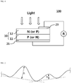
- FIG. 1 is a schematic view of a solar cell according to one embodiment of the present invention.
- the solar cell 100 may include a silicon substrate 10 and an electrode formed on the silicon substrate 10.
- the solar cell may include a front electrode 23 formed on a front surface of the silicon substrate 10.
- the silicon substrate 10 may be a substrate with a PN junction formed thereon, and a rear electrode 21 may be formed on a back surface of the silicon substrate 10.
- the silicon substrate 10 may include a semiconductor substrate 11 and an emitter 12. More specifically, the silicon substrate 10 may be a substrate prepared by doping one surface of a p-type semiconductor substrate 11 with an n-type dopant to form an n-type emitter 12.
- the substrate 10 may be a substrate prepared by doping one surface of an n-type semiconductor substrate 11 with a p-type dopant to form a p-type emitter 12.
- the semiconductor substrate 11 may be either a p-type substrate or an n-type substrate.
- the p-type substrate may be a semiconductor substrate 11 doped with a p-type dopant
- the n-type substrate may be a semiconductor substrate 11 doped with an n-type dopant.
- a surface of such a substrate through which light enters the substrate is referred to as a front surface (light receiving surface).
- a surface of the substrate opposite the front surface is referred to as a back surface.
- the semiconductor substrate 11 may be formed of crystalline silicon or a compound semiconductor.
- the crystalline silicon may be monocrystalline or polycrystalline.
- a silicon wafer may be used as the crystalline silicon.
- the p-type dopant may be a material including a group III element such as boron, aluminum, or gallium.
- the n-type dopant may be a material including a group V element, such as phosphorus, arsenic or antimony.
- the rear electrode 21 and/or the front electrode 23 may be fabricated using a composition for solar cell electrodes described below. Specifically, the rear electrode and/or the front electrode may be fabricated through a process in which the composition for solar cell electrodes is deposited on the substrate by printing, followed by baking.
- the solar cell 100 includes the silicon substrate 10 and the electrode formed on the substrate 10, wherein the silicon substrate may be formed with 5 or more, specifically 5 to 100, more specifically 5 to 50 raised portions having a height (h) of 50 nm or more per 5 ⁇ m length in sectional view.
- the silicon substrate having 5 or more raised portions can have higher surface roughness than a typical Si wafer, thereby further reducing reflectance of sunlight and can have an increased contact area with the electrode, thereby providing good properties in terms of contact resistance (Rc) and short-circuit current (Isc).
- MCCE metal catalyzed chemical etching
- SDR saw damage removal
- MCCE refers to a process of gradually etching a surface of a Si substrate with silver nitrate (AgNO 3 ), followed by removal of silver nanoparticles, i.e., byproducts.
- a representative example of dry etching is reactive ion etching (RIE) in which a silicon wafer subjected to SDR is dry-etched using plasma.
- RIE reactive ion etching
- SF 6 /O 2 gas is used to generate plasma and a SiOF layer used as a mask needs to be removed.
- a nano-texture (or the number of raised portions) of the silicon substrate is controlled by wet etching.
- the solar cell according of the present invention may further include an anti-reflection film (not shown) on the front surface of the silicon substrate 10.
- a back surface field layer (not shown), an anti-reflection film (not shown), and the rear electrode 21 may be sequentially formed on the back surface of the silicon substrate 10.
- the front electrode 23 or the rear electrode 21 may be formed in a bus bar pattern.
- the semiconductor substrate 11 is a p-type substrate.
- the present invention is not limited thereto and the semiconductor substrate 11 may be an n-type substrate.
- One surface of the p-type substrate 11 is doped with an n-type dopant to form an n-type emitter 12 to establish a PN junction.
- the PN junction may be established at an interface between the semiconductor substrate and the emitter. Electrons generated in the PN junction may be collected by the front electrode 23.
- the substrate 10 may have a textured structure on the front surface thereof.
- the textured structure may be formed by surface treatment of the front surface of the substrate 10 using a typical method known in the art, such as etching.
- the textured structure serves to condense light entering the front surface of the substrate.
- the textured structure may have a pyramidal shape, a square honeycomb shape, a triangular honeycomb shape, and the like.
- the textured structure allows an increased amount of light to reach the PN junction and reduces reflectance of light, thereby minimizing optical loss.
- the silicon substrate having the textured structure may further include raised portions, thereby further reducing reflectance of sunlight while providing further improved properties in terms of contact resistance (Rc) and short-circuit current (Isc).
- the p-type substrate may be formed on the back surface thereof with the back surface field (BSF) layer capable of inducing back surface field (BSF) effects.
- BSF back surface field
- the back surface field layer is formed by doping the back surface of the p-type semiconductor substrate 11 with a high concentration of p-type dopant.
- the back surface field layer has a higher doping concentration than the p-type semiconductor substrate 11, which results in a potential difference between the back surface field layer and the p-type semiconductor substrate 11. This makes it difficult for electrons generated in the p-type semiconductor substrate 11 to shift towards the back surface of the substrate so as to prevent recombination with metals, thereby reducing electron loss.
- both open circuit voltage (Voc) and fill factor can be increased, thereby improving solar cell efficiency.
- a first anti-reflection film (not shown) and/or a second anti-reflection film 50 may be formed on an upper surface of the n-type emitter 12 and on a lower surface of the back surface field layer, respectively.
- the first and second anti-reflection films can reduce reflectance of light while increasing absorption of light at a specific wavelength.
- the first and second anti-reflection films can enhance contact efficiency with silicon present on the surface of the silicon substrate 10, thereby improving solar cell efficiency.
- the first and second anti-reflection films may include a material that reflects less light and exhibits electric insulation.
- the first and second anti-reflection films may have an uneven surface, or may have the same form as that of the textured structure formed on the substrate. In this case, return loss of incident light can be reduced.
- the first and second anti-reflection films may include at least one of, for example, oxides including aluminum oxide (Al 2 O 3 ), silicon oxide (SiO 2 ), titanium oxide (TiO 2 or TiO 4 ), magnesium oxide (MgO), cerium oxide (CeO 2 ), or combinations thereof; nitrides including aluminum nitride (AlN), silicon nitride (SiNx), titanium nitride (TiN), or combinations thereof; and oxynitrides including aluminum oxynitride (AlON), silicon oxynitride (SiON), titanium oxynitride (TiON), or combinations thereof.
- the first and second anti-reflection films can exhibit further improved anti-reflection efficiency.
- the anti-reflection films may be formed by, for example, atomic layer deposition (ALD), vacuum deposition, atmospheric pressure chemical vapor deposition, plasma enhanced chemical vapor deposition, and the like.
- ALD atomic layer deposition
- vacuum deposition vacuum deposition
- atmospheric pressure chemical vapor deposition atmospheric pressure chemical vapor deposition
- plasma enhanced chemical vapor deposition and the like.
- the anti-reflection films may be formed of silicon nitride (SiN x ) or the like by plasma enhanced chemical vapor deposition (PECVD).
- PECVD plasma enhanced chemical vapor deposition
- the anti-reflection films may be formed of aluminum oxide (Al 2 O 3 ) or the like by atomic layer deposition (ALD).
- the first anti-reflection film may be formed on the front surface of the silicon substrate 10 and may have a monolayer or multilayer structure.
- the second anti-reflection film (not shown) may be formed on a lower surface of the back surface field layer.
- the second anti-reflection film can further increase open circuit voltage.
- the front electrode 23 electrically connected to the n-type emitter layer 12 and the rear electrode 21 electrically connected to the p-type substrate 11 may be formed.
- the front electrode 23 allows electrons collected by the n-type emitter to shift thereto.
- the rear electrode 21 electrically communicates with the p-type substrate and serves as a path through which electric current flows.
- the front electrode 23 and the rear electrode 21 may be formed of the composition for solar cell electrodes.
- the composition for solar cell electrodes may be deposited on the back surface of the PN junction substrate by printing. Then, a preliminary process of preparing the rear electrode is performed by drying at about 200°C to about 400°C for about 10 to 60 seconds. Further, a preliminary process for preparing the front electrode may be performed by printing the composition for solar cell electrodes on the front surface of the PN junction substrate, followed by drying the printed composition. Then, the front electrode and the rear electrode may be formed by baking at about 400°C to about 950°C, for example, at about 750°C to about 950°C, for about 30 to 180 seconds.
- the silicon substrate can exhibit good adhesion to the electrodes despite having the raised portions, thereby providing further improved properties in terms of contact resistance, serial resistance and the like.
- composition for solar cell electrodes according to the present invention includes a conductive powder, an organic vehicle, and a glass frit having a glass transition temperature (Tg) of ⁇ 150°C to ⁇ 450°C.
- the composition for solar cell electrodes according to the present invention may include silver (Ag) powder as the conductive powder.
- the silver powder may have a nanometer or micrometer-scale particle size.
- the silver powder may have an average particle diameter of dozens to several hundred nanometers, or an average particle diameter of several to dozens of micrometers.
- the silver powder may be a mixture of two or more types of silver powder having different particle sizes.
- the silver powder may have, for example, a spherical, flake or amorphous particle shape.
- the average particle diameter may be measured using, for example, a Model 1064D (CILAS Co., Ltd.) after dispersing the conductive powder in isopropyl alcohol (IPA) at 25°C for 3 minutes via ultrasonication.
- the conductive powder may be present in an amount of about 60 wt% to about 95 wt% based on the total weight of the composition for solar cell electrodes. Within this range, the composition can reduce resistance of a solar cell electrode, thereby improving conversion efficiency of a solar cell. In addition, the composition can be easily prepared in paste form.
- the silver powder may be present in an amount of ⁇ 60 wt% to ⁇ 95 wt%, specifically ⁇ 65 wt% to ⁇ 95 wt%, more specifically ⁇ 65 wt% to ⁇ 90 wt% based on the total weight of the composition for solar cell electrodes.
- the composition can improve conversion efficiency of a solar cell and can be easily prepared in paste form.
- the glass frit serves to form silver crystal grains in an emitter region by etching an anti-reflection layer and melting the conductive powder during a baking process of the composition for solar cell electrodes. Further, the glass frit improves adhesion of the conductive powder to a wafer and is softened to decrease the baking temperature during the baking process.
- the glass frit may have a glass transition temperature (Tg) of ⁇ 150°C to ⁇ 450°C, specifically, ⁇ 180°C to ⁇ 400°C, more specifically, ⁇ 200°C to ⁇ 350°C.
- Tg glass transition temperature
- the composition can be well deposited on a silicon substrate having raised portions and can have good adhesion to the substrate, thereby further improving electrical properties such as contact resistance and serial resistance. If the glass transition temperature (Tg) of the glass frit is less than 150°C, the composition spreads and is thus difficult to form into an electrode, whereas, if the glass transition temperature (Tg) of the glass frit exceeds 450°C, the composition cannot sufficiently permeate a space between the raised portions and thus has low adhesion to the substrate and thus poor electrical properties.
- the glass frit may have a crystallization temperature (Tc) of ⁇ 300°C to ⁇ 650°C, specifically ⁇ 300°C to ⁇ 600°C, more specifically, ⁇ 400°C to ⁇ 550°C.
- the glass frit may have a melting point (Tm) of ⁇ 350°C to ⁇ 700°C, specifically ⁇ 350°C to ⁇ 650°C, more specifically, ⁇ 400°C to ⁇ 600°C.
- Tc crystallization temperature
- Tm melting point
- the glass frit may include at least one of tellurium (Te), lithium (Li), zinc (Zn), bismuth (Bi), lead (Pb), sodium (Na), phosphorus (P), germanium (Ge), gallium (Ga), cerium (Ce), iron (Fe), silicon (Si), tungsten (W), magnesium (Mg), molybdenum (Mo), cesium (Cs), strontium (Sr), titanium (Ti), tin (Sn), indium (In), vanadium (V), barium (Ba), nickel (Ni), copper (Cu), potassium (K), arsenic (As), cobalt (Co), zirconium (Zr), manganese (Mn), aluminum (Al), and boron (B).
- the glass frit may be formed of an oxide of the at least one elemental metal.
- the glass frit may include at least one selected from among Bi-Te-O glass frits, Pb-Bi-O glass frits, Pb-Te-O glass frits, Te-B-O glass frits, Te-Ag-O glass frits, Pb-Si-O glass frits, Bi-Si-O glass frits, Te-Zn-O glass frits, Bi-B-O glass frits, Pb-B-O glass frits, Bi-Mo-O glass frits, Mo-B-O glass frits, and Te-Si-O glass frits.
- a solar cell electrode formed of the composition can exhibit good balance between electrical properties.
- the glass frit may be prepared by any suitable method known in the art.
- the glass frit may be prepared by mixing the aforementioned components using a ball mill or a planetary mill, melting the mixture at 900°C to 1300°C, and quenching the melted mixture to 25°C, followed by pulverizing the obtained product using a disk mill, a planetary mill or the like.
- the glass frit may have an average particle diameter (D50) of ⁇ 0.1 ⁇ m to ⁇ 10 ⁇ m, specifically, ⁇ 0.1 ⁇ m to ⁇ 7 ⁇ m, more specifically, ⁇ 0.1 ⁇ m to ⁇ 5 ⁇ m.
- D50 means that at least 50% percent of the particles have a diameter of 0.1 ⁇ m to 10 ⁇ m.
- the glass frit may be present in an amount of ⁇ 0.1 wt% to ⁇ 20 wt%, specifically ⁇ 0.5 wt% to ⁇ 10 wt%, more specifically ⁇ 0.5 wt% to ⁇ 7 wt% based on the total weight of the composition for solar cell electrodes. Within this range, the glass frit can secure stability of a PN junction under various sheet resistances, minimize resistance, and ultimately improve the efficiency of a solar cell.
- the organic vehicle imparts suitable viscosity and rheological characteristics for printing to the composition for solar cell electrodes through mechanical mixing with inorganic components of the composition.
- the organic vehicle may be any typical organic vehicle used in a composition for solar cell electrodes and may generally include a binder resin, a solvent, and the like.
- the binder resin may be acrylate resins or cellulose resins. Ethyl cellulose is generally used as the binder resin. In addition, the binder resin may be ethyl hydroxyethyl cellulose, nitrocellulose, blends of ethyl cellulose and phenol resins, alkyd resins, phenol resins, acrylate ester resins, xylene resins, polybutane resins, polyester resins, urea resins, melamine resins, vinyl acetate resins, wood rosin, polymethacrylates of alcohols, and the like.
- the solvent may include at least one of, for example, hexane, toluene, ethyl cellosolve, cyclohexanone, butyl cellosolve, butyl carbitol (diethylene glycol monobutyl ether), dibutyl carbitol (diethylene glycol dibutyl ether), butyl carbitol acetate (diethylene glycol monobutyl ether acetate), propylene glycol monomethyl ether, hexylene glycol, terpineol, methylethylketone, benzyl alcohol, ⁇ -butyrolactone, ethyl lactate, and mixtures thereof.
- butyl carbitol diethylene glycol monobutyl ether
- dibutyl carbitol diethylene glycol dibutyl ether
- butyl carbitol acetate diethylene glycol monobutyl ether acetate
- propylene glycol monomethyl ether
- the organic vehicle may be present in an amount of ⁇ 1 wt% to ⁇ 30 wt%, specifically ⁇ 1 wt% to ⁇ 25 wt%, more specifically ⁇ 1 wt% to ⁇ 10 wt% in the composition for solar cell electrodes. Within this range, the organic vehicle can provide sufficient adhesive strength and good printability to the composition.
- the composition for solar cell electrodes according to the present invention may further include any typical additive to enhance flowability, processability and stability, as needed.
- the additive may include a dispersant, a thixotropic agent, a plasticizer, a viscosity stabilizer, an anti-foaming agent, a pigment, a UV stabilizer, an antioxidant, a coupling agent, and the like. These may be used alone or as a mixture thereof.
- the additive may be present in an amount of 0.1 wt% to 5 wt% based on the total weight of the composition for solar cell electrodes, although the content of the additive may be changed, as needed.
- ethylcellulose As an organic binder, 1.6 wt% of ethylcellulose (STD4, Dow Chemical Company) was sufficiently dissolved in 5.1 wt% of butyl carbitol at 60°C, and then 88.9 wt% of spherical silver powder (AG-4-8, Dowa Hightech Co., Ltd.) having an average particle diameter of 2.0 ⁇ m, 3.1 wt% of a Pb-Te-O glass frit having an average particle diameter of 1.0 ⁇ m (Tg: 275°C, Tc: 410°C, Tm: 530°C), 0.5 wt% of a dispersant (BYK102, BYK-chemie), and 0.8 wt% of a thixotropic agent (Thixatrol ST, Elementis Co., Ltd.) were added to the binder solution, followed by mixing and kneading in a 3-roll kneader, thereby preparing a composition for solar cell
- the composition was deposited onto a front surface of a silicon substrate ((average) number of raised portions: 9) by screen printing in a predetermined pattern, followed by drying in an IR drying furnace.
- a cell formed according to this procedure was subjected to baking at 600°C to 900°C for 60 to 210 seconds in a belt-type baking furnace, thereby fabricating a solar cell.
- Rs serial resistance
- the solar cells of Comparative Examples 3 to 4 in which the number of raised portions of the silicon substrate was less than the range set forth herein had high serial resistance (Rs) and thus low conversion efficiency (Eff.)
Landscapes
- Chemical & Material Sciences (AREA)
- Life Sciences & Earth Sciences (AREA)
- Engineering & Computer Science (AREA)
- Geochemistry & Mineralogy (AREA)
- Chemical Kinetics & Catalysis (AREA)
- General Chemical & Material Sciences (AREA)
- Materials Engineering (AREA)
- Organic Chemistry (AREA)
- Spectroscopy & Molecular Physics (AREA)
- Dispersion Chemistry (AREA)
- Physics & Mathematics (AREA)
- Photovoltaic Devices (AREA)
- Sustainable Development (AREA)
- Sustainable Energy (AREA)
- Glass Compositions (AREA)
- Conductive Materials (AREA)
Abstract
Description
- This application claims the benefit of Korean Patent Application
10-2017-0168655, filed on December 08, 2017 - The present invention relates to a solar cell.
- Solar cells generate electricity using the photovoltaic effect of a PN junction which converts photons of sunlight into electricity. In a solar cell, front and rear electrodes are formed on upper and lower surfaces of a semiconductor wafer or substrate having a PN junction, respectively. Then, the photovoltaic effect at the PN junction is induced by sunlight entering the semiconductor wafer and electrons generated by the photovoltaic effect at the PN junction provide electric current to the outside through the electrodes. The electrodes of the solar cell are formed on the wafer by applying, patterning, and baking a composition for solar cell electrodes.
- In order to reduce reflectance of light incident on a solar cell to improve efficiency of the solar cell, there has been proposed a method in which a surface of a substrate is textured and/or is formed with an anti-reflection film. However, this method cannot provide sufficient anti-reflection properties.
- In addition, the method has a problem in that an electrode can have poor adhesion to the substrate having a textured surface.
- Therefore, there is a need for a solar cell which can reduce reflection of light incident thereon and improve adhesion of an electrode to a substrate, thereby exhibiting good electrical properties, such as contact resistance, serial resistance, short-circuit current and conversion efficiency.
- The background technique of the present invention is disclosed in Japanese Unexamined Patent Publication No.
2012-084585 - It is one aspect of the present invention to provide a solar cell which can reduce reflectance, thereby exhibiting improved conversion efficiency.
- It is another aspect of the present invention to provide a solar cell which can improve adhesion of an electrode to a substrate, thereby exhibiting good electrical properties, such as contact resistance, serial resistance and short-circuit current.
- These and other objects of the present invention can be achieved by embodiments of the present invention described below.
- An aspect of the present invention relates to a solar cell.
- The solar cell includes: a silicon substrate; and an electrode formed on the silicon substrate, wherein the silicon substrate is formed with at least 5 raised portions having a cross-sectional height (h) of 50 nm or more per 5 µm length, and the electrode is formed of a composition for solar cell electrodes including a conductive powder, an organic vehicle, and a glass frit having a glass transition temperature (Tg) of 150°C to 450°C.
- The glass frit may have a crystallization temperature (Tc) of 300°C to 650°C.
- The glass frit may have a melting point (Tm) of 350°C to 700°C.
- The glass frit may be formed of a metal oxide, wherein the metal oxide may include at least one elemental metal selected from among tellurium (Te), lithium (Li), zinc (Zn), bismuth (Bi), lead (Pb), sodium (Na), phosphorus (P), germanium (Ge), gallium (Ga), cerium (Ce), iron (Fe), silicon (Si), tungsten (W), magnesium (Mg), molybdenum (Mo), cesium (Cs), strontium (Sr), titanium (Ti), tin (Sn), indium (In), vanadium (V), barium (Ba), nickel (Ni), copper (Cu), potassium (K), arsenic (As), cobalt (Co), zirconium (Zr), manganese (Mn), aluminum (Al), and boron (B).
- The glass frit may include at least one selected from among Bi-Te-O glass frits, Pb-Bi-O glass frits, Pb-Te-O glass frits, Te-B-O glass frits, Te-Ag-O glass frits, Pb-Si-O glass frits, Bi-Si-O glass frits, Te-Zn-O glass frits, Bi-B-O glass frits, Pb-B-O glass frits, Bi-MoO glass frits, Mo-B-O glass frits, and Te-Si-O glass frits.
- The glass frit may have an average particle diameter of 0.1 µm to 10 µm.
- The composition for solar cell electrodes may include: 60 wt% to 95 wt% of the conductive powder; 0.1 wt% to 20 wt% of the glass frit; and 1 wt% to 30 wt% of the organic vehicle.
- The composition for solar cell electrodes may further include at least one additive selected from among a dispersant, a thixotropic agent, a plasticizer, a viscosity stabilizer, an anti-foaming agent, a pigment, a UV stabilizer, an antioxidant, and a coupling agent.
- The present invention provides a solar cell which can reduce reflectance, thereby exhibiting improved conversion efficiency and can improve adhesion of an electrode to a substrate, thereby exhibiting good electrical properties, such as contact resistance, serial resistance and short-circuit current.
-
-
FIG. 1 is a schematic view of a solar cell according to one embodiment of the present invention. -
Fig. 2 is a view illustrating the definition of a raised portion according to the present invention. -
FIG. 3 is an electron microscope image showing a raised portion of a solar cell according to the present invention. -
FIG. 4 is an electron microscope image of Comparative Example 3 (a surface of a typical substrate). -
FIG. 5 is an electron microscope image of a surface of a substrate according to Example of the present invention. - Hereinafter, embodiments of the present invention will be described in detail.
- Description of known functions and constructions which may unnecessarily obscure the subject matter of the present invention will be omitted.
- As used herein, the singular forms, "a," "an," and "the" are intended to include the plural forms as well, unless context clearly indicates otherwise. Moreover, the terms "comprises," "comprising," "includes," and/or "including," when used in this specification, specify the presence of stated features, integers, steps, operations, elements, components, and/or groups thereof, but do not preclude the presence or addition of one or more other features, integers, steps, operations, elements, components, and/or groups thereof.
- In addition, unless stated otherwise, a margin of error is considered in analysis of components.
- As used herein, the term "metal oxide" may refer to one metal oxide or a plurality of metal oxides.
- Further, "X to Y", as used herein to represent a range of a certain value means "greater than or equal to X and less than or equal to Y".
- As used herein, the phrase "a substrate has a raised portion having a height (h) of 50 nm or more" means that the portion is higher than the surrounding surface and has a diameter of 500 nm or less, and a vertical distance from the summit of the portion to a line connecting both sides of the portion is 50 nm or more in sectional view of the silicon substrate (see
FIG. 2 ).FIG. 3 is an actual sectional image of a silicon substrate for defining a raised portion according to the present invention. - A solar cell according to one embodiment of the present invention will be described with reference to
FIG. 1. FIG. 1 is a schematic view of a solar cell according to one embodiment of the present invention. - The
solar cell 100 according to this embodiment may include asilicon substrate 10 and an electrode formed on thesilicon substrate 10. Specifically, the solar cell may include afront electrode 23 formed on a front surface of thesilicon substrate 10. Thesilicon substrate 10 may be a substrate with a PN junction formed thereon, and arear electrode 21 may be formed on a back surface of thesilicon substrate 10. Specifically, thesilicon substrate 10 may include asemiconductor substrate 11 and anemitter 12. More specifically, thesilicon substrate 10 may be a substrate prepared by doping one surface of a p-type semiconductor substrate 11 with an n-type dopant to form an n-type emitter 12. Alternatively, thesubstrate 10 may be a substrate prepared by doping one surface of an n-type semiconductor substrate 11 with a p-type dopant to form a p-type emitter 12. Here, thesemiconductor substrate 11 may be either a p-type substrate or an n-type substrate. The p-type substrate may be asemiconductor substrate 11 doped with a p-type dopant, and the n-type substrate may be asemiconductor substrate 11 doped with an n-type dopant. - In description of the
silicon substrate 10, thesemiconductor substrate 11 and the like, a surface of such a substrate through which light enters the substrate is referred to as a front surface (light receiving surface). In addition, a surface of the substrate opposite the front surface is referred to as a back surface. - In one embodiment, the
semiconductor substrate 11 may be formed of crystalline silicon or a compound semiconductor. Here, the crystalline silicon may be monocrystalline or polycrystalline. As the crystalline silicon, for example, a silicon wafer may be used. - Here, the p-type dopant may be a material including a group III element such as boron, aluminum, or gallium. In addition, the n-type dopant may be a material including a group V element, such as phosphorus, arsenic or antimony.
- The
rear electrode 21 and/or thefront electrode 23 may be fabricated using a composition for solar cell electrodes described below. Specifically, the rear electrode and/or the front electrode may be fabricated through a process in which the composition for solar cell electrodes is deposited on the substrate by printing, followed by baking. - The
solar cell 100 according to this embodiment includes thesilicon substrate 10 and the electrode formed on thesubstrate 10, wherein the silicon substrate may be formed with 5 or more, specifically 5 to 100, more specifically 5 to 50 raised portions having a height (h) of 50 nm or more per 5 µm length in sectional view. - The silicon substrate having 5 or more raised portions can have higher surface roughness than a typical Si wafer, thereby further reducing reflectance of sunlight and can have an increased contact area with the electrode, thereby providing good properties in terms of contact resistance (Rc) and short-circuit current (Isc).
- There are two primary methods to form a nano-texture (or raised portions) on the silicon substrate: wet etching and dry etching. A representative example of wet etching is metal catalyzed chemical etching (MCCE). For example, saw damage caused by diamond sawing is removed through a saw damage removal (SDR) process, followed by formation of a nano-texture through MCCE. Herein, "MCCE" refers to a process of gradually etching a surface of a Si substrate with silver nitrate (AgNO3), followed by removal of silver nanoparticles, i.e., byproducts. A representative example of dry etching is reactive ion etching (RIE) in which a silicon wafer subjected to SDR is dry-etched using plasma. Here, SF6/O2 gas is used to generate plasma and a SiOF layer used as a mask needs to be removed.
- In the present invention, a nano-texture (or the number of raised portions) of the silicon substrate is controlled by wet etching.
- In another embodiment, the solar cell according of the present invention may further include an anti-reflection film (not shown) on the front surface of the
silicon substrate 10. In addition, a back surface field layer (not shown), an anti-reflection film (not shown), and therear electrode 21 may be sequentially formed on the back surface of thesilicon substrate 10. Here, thefront electrode 23 or therear electrode 21 may be formed in a bus bar pattern. - Hereinafter, for convenience of explanation, each component of the solar cell according to the present invention will be described on the assumption that the
semiconductor substrate 11 is a p-type substrate. However, it should be understood that the present invention is not limited thereto and thesemiconductor substrate 11 may be an n-type substrate. - One surface of the p-
type substrate 11 is doped with an n-type dopant to form an n-type emitter 12 to establish a PN junction. Here, the PN junction may be established at an interface between the semiconductor substrate and the emitter. Electrons generated in the PN junction may be collected by thefront electrode 23. - The
substrate 10 may have a textured structure on the front surface thereof. The textured structure may be formed by surface treatment of the front surface of thesubstrate 10 using a typical method known in the art, such as etching. The textured structure serves to condense light entering the front surface of the substrate. The textured structure may have a pyramidal shape, a square honeycomb shape, a triangular honeycomb shape, and the like. Thus, the textured structure allows an increased amount of light to reach the PN junction and reduces reflectance of light, thereby minimizing optical loss. - According to the present invention, the silicon substrate having the textured structure may further include raised portions, thereby further reducing reflectance of sunlight while providing further improved properties in terms of contact resistance (Rc) and short-circuit current (Isc).
- The p-type substrate may be formed on the back surface thereof with the back surface field (BSF) layer capable of inducing back surface field (BSF) effects.
- The back surface field layer is formed by doping the back surface of the p-
type semiconductor substrate 11 with a high concentration of p-type dopant. The back surface field layer has a higher doping concentration than the p-type semiconductor substrate 11, which results in a potential difference between the back surface field layer and the p-type semiconductor substrate 11. This makes it difficult for electrons generated in the p-type semiconductor substrate 11 to shift towards the back surface of the substrate so as to prevent recombination with metals, thereby reducing electron loss. As a result, both open circuit voltage (Voc) and fill factor can be increased, thereby improving solar cell efficiency. - In addition, a first anti-reflection film (not shown) and/or a second anti-reflection film 50 may be formed on an upper surface of the n-
type emitter 12 and on a lower surface of the back surface field layer, respectively. - The first and second anti-reflection films can reduce reflectance of light while increasing absorption of light at a specific wavelength. In addition, the first and second anti-reflection films can enhance contact efficiency with silicon present on the surface of the
silicon substrate 10, thereby improving solar cell efficiency. Accordingly, the first and second anti-reflection films may include a material that reflects less light and exhibits electric insulation. Further, the first and second anti-reflection films may have an uneven surface, or may have the same form as that of the textured structure formed on the substrate. In this case, return loss of incident light can be reduced. - The first and second anti-reflection films may include at least one of, for example, oxides including aluminum oxide (Al2O3), silicon oxide (SiO2), titanium oxide (TiO2 or TiO4), magnesium oxide (MgO), cerium oxide (CeO2), or combinations thereof; nitrides including aluminum nitride (AlN), silicon nitride (SiNx), titanium nitride (TiN), or combinations thereof; and oxynitrides including aluminum oxynitride (AlON), silicon oxynitride (SiON), titanium oxynitride (TiON), or combinations thereof. In this case, the first and second anti-reflection films can exhibit further improved anti-reflection efficiency.
- The anti-reflection films may be formed by, for example, atomic layer deposition (ALD), vacuum deposition, atmospheric pressure chemical vapor deposition, plasma enhanced chemical vapor deposition, and the like.
- In one embodiment, the anti-reflection films may be formed of silicon nitride (SiNx) or the like by plasma enhanced chemical vapor deposition (PECVD). By way of another example, the anti-reflection films may be formed of aluminum oxide (Al2O3) or the like by atomic layer deposition (ALD).
- In one embodiment, the first anti-reflection film may be formed on the front surface of the
silicon substrate 10 and may have a monolayer or multilayer structure. - When the back surface of the p-
type semiconductor substrate 11 is doped with boron to form the back surface field layer, the second anti-reflection film (not shown) may be formed on a lower surface of the back surface field layer. The second anti-reflection film can further increase open circuit voltage. - After formation of the anti-reflection films, the
front electrode 23 electrically connected to the n-type emitter layer 12 and therear electrode 21 electrically connected to the p-type substrate 11 may be formed. Thefront electrode 23 allows electrons collected by the n-type emitter to shift thereto. Therear electrode 21 electrically communicates with the p-type substrate and serves as a path through which electric current flows. - In this embodiment, the
front electrode 23 and therear electrode 21 may be formed of the composition for solar cell electrodes. - For example, the composition for solar cell electrodes may be deposited on the back surface of the PN junction substrate by printing. Then, a preliminary process of preparing the rear electrode is performed by drying at about 200°C to about 400°C for about 10 to 60 seconds. Further, a preliminary process for preparing the front electrode may be performed by printing the composition for solar cell electrodes on the front surface of the PN junction substrate, followed by drying the printed composition. Then, the front electrode and the rear electrode may be formed by baking at about 400°C to about 950°C, for example, at about 750°C to about 950°C, for about 30 to 180 seconds.
- When the front electrode or the rear electrode according to this embodiment of the present invention is formed of the composition for solar cell electrodes described below, the silicon substrate can exhibit good adhesion to the electrodes despite having the raised portions, thereby providing further improved properties in terms of contact resistance, serial resistance and the like.
- The composition for solar cell electrodes according to the present invention includes a conductive powder, an organic vehicle, and a glass frit having a glass transition temperature (Tg) of ≥ 150°C to ≤ 450°C.
- Now, each component of the composition for solar cell electrodes according to the present invention will be described in more detail.
- The composition for solar cell electrodes according to the present invention may include silver (Ag) powder as the conductive powder. The silver powder may have a nanometer or micrometer-scale particle size. For example, the silver powder may have an average particle diameter of dozens to several hundred nanometers, or an average particle diameter of several to dozens of micrometers. Alternatively, the silver powder may be a mixture of two or more types of silver powder having different particle sizes.
- The silver powder may have, for example, a spherical, flake or amorphous particle shape.
- The average particle diameter may be measured using, for example, a Model 1064D (CILAS Co., Ltd.) after dispersing the conductive powder in isopropyl alcohol (IPA) at 25°C for 3 minutes via ultrasonication. The conductive powder may be present in an amount of about 60 wt% to about 95 wt% based on the total weight of the composition for solar cell electrodes. Within this range, the composition can reduce resistance of a solar cell electrode, thereby improving conversion efficiency of a solar cell. In addition, the composition can be easily prepared in paste form. Specifically, the silver powder may be present in an amount of ≥ 60 wt% to ≤ 95 wt%, specifically ≥ 65 wt% to ≤ 95 wt%, more specifically ≥ 65 wt% to ≤ 90 wt% based on the total weight of the composition for solar cell electrodes. Within this range, the composition can improve conversion efficiency of a solar cell and can be easily prepared in paste form.
- The glass frit serves to form silver crystal grains in an emitter region by etching an anti-reflection layer and melting the conductive powder during a baking process of the composition for solar cell electrodes. Further, the glass frit improves adhesion of the conductive powder to a wafer and is softened to decrease the baking temperature during the baking process.
- The glass frit may have a glass transition temperature (Tg) of ≥ 150°C to ≤ 450°C, specifically, ≥ 180°C to ≤ 400°C, more specifically, ≥ 200°C to ≤ 350°C. Within this range, the composition can be well deposited on a silicon substrate having raised portions and can have good adhesion to the substrate, thereby further improving electrical properties such as contact resistance and serial resistance. If the glass transition temperature (Tg) of the glass frit is less than 150°C, the composition spreads and is thus difficult to form into an electrode, whereas, if the glass transition temperature (Tg) of the glass frit exceeds 450°C, the composition cannot sufficiently permeate a space between the raised portions and thus has low adhesion to the substrate and thus poor electrical properties.
- The glass frit may have a crystallization temperature (Tc) of ≥ 300°C to ≤ 650°C, specifically ≥ 300°C to ≤ 600°C, more specifically, ≥ 400°C to ≤ 550°C. In addition, the glass frit may have a melting point (Tm) of ≥ 350°C to ≤ 700°C, specifically ≥ 350°C to ≤ 650°C, more specifically, ≥ 400°C to ≤ 600°C. When the crystallization temperature (Tc) and the melting point (Tm) of the glass frit fall within these ranges, an electrode formed of the composition can have further improved adhesion to the silicon substrate.
- The glass frit may include at least one of tellurium (Te), lithium (Li), zinc (Zn), bismuth (Bi), lead (Pb), sodium (Na), phosphorus (P), germanium (Ge), gallium (Ga), cerium (Ce), iron (Fe), silicon (Si), tungsten (W), magnesium (Mg), molybdenum (Mo), cesium (Cs), strontium (Sr), titanium (Ti), tin (Sn), indium (In), vanadium (V), barium (Ba), nickel (Ni), copper (Cu), potassium (K), arsenic (As), cobalt (Co), zirconium (Zr), manganese (Mn), aluminum (Al), and boron (B). The glass frit may be formed of an oxide of the at least one elemental metal.
- For example, the glass frit may include at least one selected from among Bi-Te-O glass frits, Pb-Bi-O glass frits, Pb-Te-O glass frits, Te-B-O glass frits, Te-Ag-O glass frits, Pb-Si-O glass frits, Bi-Si-O glass frits, Te-Zn-O glass frits, Bi-B-O glass frits, Pb-B-O glass frits, Bi-Mo-O glass frits, Mo-B-O glass frits, and Te-Si-O glass frits. In this case, a solar cell electrode formed of the composition can exhibit good balance between electrical properties.
- The glass frit may be prepared by any suitable method known in the art. For example, the glass frit may be prepared by mixing the aforementioned components using a ball mill or a planetary mill, melting the mixture at 900°C to 1300°C, and quenching the melted mixture to 25°C, followed by pulverizing the obtained product using a disk mill, a planetary mill or the like. The glass frit may have an average particle diameter (D50) of ≥ 0.1 µm to ≤ 10 µm, specifically, ≥ 0.1 µm to ≤ 7 µm, more specifically, ≥ 0.1 µm to ≤ 5 µm.
- In the present specification D50 means that at least 50% percent of the particles have a diameter of 0.1 µm to 10 µm.
- The glass frit may be present in an amount of ≥ 0.1 wt% to ≤ 20 wt%, specifically ≥ 0.5 wt% to ≤ 10 wt%, more specifically ≥ 0.5 wt% to ≤ 7 wt% based on the total weight of the composition for solar cell electrodes. Within this range, the glass frit can secure stability of a PN junction under various sheet resistances, minimize resistance, and ultimately improve the efficiency of a solar cell.
- The organic vehicle imparts suitable viscosity and rheological characteristics for printing to the composition for solar cell electrodes through mechanical mixing with inorganic components of the composition.
- The organic vehicle may be any typical organic vehicle used in a composition for solar cell electrodes and may generally include a binder resin, a solvent, and the like.
- The binder resin may be acrylate resins or cellulose resins. Ethyl cellulose is generally used as the binder resin. In addition, the binder resin may be ethyl hydroxyethyl cellulose, nitrocellulose, blends of ethyl cellulose and phenol resins, alkyd resins, phenol resins, acrylate ester resins, xylene resins, polybutane resins, polyester resins, urea resins, melamine resins, vinyl acetate resins, wood rosin, polymethacrylates of alcohols, and the like.
- The solvent may include at least one of, for example, hexane, toluene, ethyl cellosolve, cyclohexanone, butyl cellosolve, butyl carbitol (diethylene glycol monobutyl ether), dibutyl carbitol (diethylene glycol dibutyl ether), butyl carbitol acetate (diethylene glycol monobutyl ether acetate), propylene glycol monomethyl ether, hexylene glycol, terpineol, methylethylketone, benzyl alcohol, γ-butyrolactone, ethyl lactate, and mixtures thereof.
- The organic vehicle may be present in an amount of ≥ 1 wt% to ≤ 30 wt%, specifically ≥ 1 wt% to ≤ 25 wt%, more specifically ≥ 1 wt% to ≤ 10 wt% in the composition for solar cell electrodes. Within this range, the organic vehicle can provide sufficient adhesive strength and good printability to the composition.
- The composition for solar cell electrodes according to the present invention may further include any typical additive to enhance flowability, processability and stability, as needed. The additive may include a dispersant, a thixotropic agent, a plasticizer, a viscosity stabilizer, an anti-foaming agent, a pigment, a UV stabilizer, an antioxidant, a coupling agent, and the like. These may be used alone or as a mixture thereof. The additive may be present in an amount of 0.1 wt% to 5 wt% based on the total weight of the composition for solar cell electrodes, although the content of the additive may be changed, as needed.
- Next, the present invention will be described in more detail with reference to examples. However, it should be noted that these examples are provided for illustration only and should not be construed in any way as limiting the invention.
- In addition, description of details apparent to those skilled in the art will be omitted for clarity.
- As an organic binder, 1.6 wt% of ethylcellulose (STD4, Dow Chemical Company) was sufficiently dissolved in 5.1 wt% of butyl carbitol at 60°C, and then 88.9 wt% of spherical silver powder (AG-4-8, Dowa Hightech Co., Ltd.) having an average particle diameter of 2.0 µm, 3.1 wt% of a Pb-Te-O glass frit having an average particle diameter of 1.0 µm (Tg: 275°C, Tc: 410°C, Tm: 530°C), 0.5 wt% of a dispersant (BYK102, BYK-chemie), and 0.8 wt% of a thixotropic agent (Thixatrol ST, Elementis Co., Ltd.) were added to the binder solution, followed by mixing and kneading in a 3-roll kneader, thereby preparing a composition for solar cell electrodes.
- The composition was deposited onto a front surface of a silicon substrate ((average) number of raised portions: 9) by screen printing in a predetermined pattern, followed by drying in an IR drying furnace. A cell formed according to this procedure was subjected to baking at 600°C to 900°C for 60 to 210 seconds in a belt-type baking furnace, thereby fabricating a solar cell.
- Solar cells were fabricated in the same manner as in Example 1 except that silicon substrates and glass frits listed in Table 1 were used.
Table 1 Silicon substrate ((average) number of raised portions) Glass frit Example 1 9 Pb-Te-O glass frit (Tg: 241°C, Tc: 410°C, Tm: 485°C) Example 2 14 Te-Ag-O glass frit (Tg: 175°C, Tc: 267°C, Tm: 395°C) Example 3 19 Mo-B-O glass frit (Tg: 445°C, Tc: 505°C, Tm: 668°C) Example 4 5 Pb-Si-O glass frit (Tg: 271°C, Tc: 420°C, Tm: 630°C) Example 5 17 Pb-Te-O glass frit (Tg: 246°C, Tc: 395°C, Tm: 565°C) Example 6 23 Bi-Te-O glass frit (Tg: 296°C, Tc: 419°C, Tm: 611°C) Comparative Example 1 11 Te-Ag-O glass frit (Tg: 146°C, Tc: 327°C, Tm: 441°C) Comparative Example 2 16 Bi-Mo-O glass frit (Tg: 490°C, Tc: 523°C, Tm: 710°C) Comparative Example 3 2 Pb-Te-O glass frit (Tg: 263°C, Tc: 330°C, Tm: 621°C) Comparative Example 4 0 Pb-Te-O glass frit (Tg: 263°C, Tc: 330°C, Tm: 621°C) -
- (1) Number of raised portions: The number of raised portions having a height (h) of 50 nm or more per 5 µm length was measured ten times using an electron microscope image of the cross section of each of the solar cells fabricated in Examples and Comparative Examples, followed by averaging the values. Results are shown in Table 1.
- (2) Serial resistance (Rs, Ω), fill factor (%) and efficiency (%): Each of the compositions for solar cell electrodes prepared in Examples and Comparative Examples was deposited onto a front surface of a wafer by screen printing in a predetermined pattern, followed by drying in an IR drying furnace. Then, an aluminum paste was printed onto a back surface of the wafer and dried in the same manner as above. A cell formed according to this procedure was subjected to baking at 400°C to 900°C for 30 to 180 seconds in a belt-type baking furnace, and then evaluated as to serial resistance (Rs, Ω), fill factor (FF, %) and conversion efficiency (Eff., %) using a solar cell efficiency tester CT-801 (Pasan Co., Ltd.). Results are shown in Table 2.
- As shown in Table 2, it can be seen that the solar cells of Examples 1 to 6 in which the number of raised portions and the glass transition temperature of the glass frit fell within the ranges set forth herein had excellent serial resistance (Rs) and thus high fill factor (FF) and conversion efficiency (Eff.)
- Conversely, the solar cell of Comparative Example 1 in which the glass transition temperature of the glass frit was less than the range set forth herein had high serial resistance (Rs) due to formation of a thick glass layer (i.e, an insulator) between Si and an Ag electrode, and the solar cell of Comparative Example 2 in which the glass transition temperature of the glass frit exceeded the range set forth herein had high serial resistance (Rs) due to poor flowability and thus poor ARC etching performance.
- In addition, the solar cells of Comparative Examples 3 to 4 in which the number of raised portions of the silicon substrate was less than the range set forth herein had high serial resistance (Rs) and thus low conversion efficiency (Eff.)
- Although some embodiments have been described herein, it should be understood that these embodiments are provided for illustration only and are not to be construed in any way as limiting the present invention, and that various modifications, changes, alterations, and equivalent embodiments can be made by those skilled in the art without departing from the spirit and scope of the invention. The scope of the present invention should be defined by the appended claims and equivalents thereof.
-
- 10: substrate
- 11: semiconductor substrate
- 12: emitter
- 21: rear electrode
- 23: front electrode
| Serial resistance (Ω) | FF (%) | Eff. (%) | |
| Example 1 | 0.002471 | 78.85 | 18.19 |
| Example 2 | 0.002962 | 78.39 | 18.10 |
| Example 3 | 0.003078 | 78.20 | 18.03 |
| Example 4 | 0.002887 | 78.43 | 18.11 |
| Example 5 | 0.002349 | 78.99 | 18.23 |
| Example 6 | 0.002455 | 78.89 | 18.20 |
| Comparative Example 1 | 0.003465 | 77.56 | 17.74 |
| Comparative Example 2 | 0.003381 | 77.28 | 17.64 |
| Comparative Example 3 | 0.004073 | 77.03 | 17.45 |
| Comparative Example 4 | 0.018874 | 55.89 | 14.18 |
Claims (8)
- A solar cell comprising:a silicon substrate; andan electrode formed on the silicon substrate,wherein the silicon substrate is formed with at least 5 raised portions having a cross-sectional height (h) of 50 nm or more per 5 µm length, andthe electrode is formed of a composition for solar cell electrodes comprising a conductive powder, an organic vehicle, and a glass frit having a glass transition temperature (Tg) of 150°C to 450°C.
- The solar cell according to claim 1, wherein the glass frit has a crystallization temperature (Tc) of 300°C to 650°C.
- The solar cell according to claim 1 or 2, wherein the glass frit has a melting point (Tm) of 350°C to 700°C.
- The solar cell according to claims 1 to 3, wherein the glass frit is formed of a metal oxide, the metal oxide comprising at least one elemental metal selected from among tellurium (Te), lithium (Li), zinc (Zn), bismuth (Bi), lead (Pb), sodium (Na), phosphorus (P), germanium (Ge), gallium (Ga), cerium (Ce), iron (Fe), silicon (Si), tungsten (W), magnesium (Mg), molybdenum (Mo), cesium (Cs), strontium (Sr), titanium (Ti), tin (Sn), indium (In), vanadium (V), barium (Ba), nickel (Ni), copper (Cu), potassium (K), arsenic (As), cobalt (Co), zirconium (Zr), manganese (Mn), aluminum (Al), and boron (B).
- The solar cell according to claims 1 to 4, wherein the glass frit comprises at least one selected from among Bi-Te-O glass frits, Pb-Bi-O glass frits, Pb-Te-O glass frits, Te-B-O glass frits, Te-Ag-O glass frits, Pb-Si-O glass frits, Bi-Si-O glass frits, Te-Zn-O glass frits, Bi-B-O glass frits, Pb-B-O glass frits, Bi-Mo-O glass frits, Mo-B-O glass frits, and Te-Si-O glass frits.
- The solar cell according to claims 1 to 5, wherein the glass frit has an average particle diameter of 0.1 µm to 10 µm.
- The solar cell according to claims 1 to 6, wherein the composition for solar cell electrodes comprises: 60 wt% to 95 wt% of the conductive powder; 0.1 wt% to 20 wt% of the glass frit; and 1 wt% to 30 wt% of the organic vehicle.
- The solar cell according to claims 1 to 7, wherein the composition for solar cell electrodes further comprises at least one additive selected from among a dispersant, a thixotropic agent, a plasticizer, a viscosity stabilizer, an anti-foaming agent, a pigment, a UV stabilizer, an antioxidant, and a coupling agent.
Applications Claiming Priority (1)
| Application Number | Priority Date | Filing Date | Title |
|---|---|---|---|
| KR1020170168655A KR20190068351A (en) | 2017-12-08 | 2017-12-08 | Solar cell |
Publications (2)
| Publication Number | Publication Date |
|---|---|
| EP3496156A1 true EP3496156A1 (en) | 2019-06-12 |
| EP3496156B1 EP3496156B1 (en) | 2021-09-15 |
Family
ID=62947986
Family Applications (1)
| Application Number | Title | Priority Date | Filing Date |
|---|---|---|---|
| EP18183100.9A Active EP3496156B1 (en) | 2017-12-08 | 2018-07-12 | Solar cell |
Country Status (6)
| Country | Link |
|---|---|
| US (1) | US20190181277A1 (en) |
| EP (1) | EP3496156B1 (en) |
| JP (1) | JP2019106524A (en) |
| KR (1) | KR20190068351A (en) |
| CN (1) | CN109904242A (en) |
| TW (1) | TWI721279B (en) |
Cited By (1)
| Publication number | Priority date | Publication date | Assignee | Title |
|---|---|---|---|---|
| CN116403756A (en) * | 2023-04-21 | 2023-07-07 | 浙江奕成科技有限公司 | Front silver paste of N-type solar cell and preparation method and application thereof |
Families Citing this family (1)
| Publication number | Priority date | Publication date | Assignee | Title |
|---|---|---|---|---|
| WO2021119428A2 (en) * | 2019-12-12 | 2021-06-17 | Bert Thin Films, Llc | Pastes for solar cells, solar cells, and methods of making same |
Citations (3)
| Publication number | Priority date | Publication date | Assignee | Title |
|---|---|---|---|---|
| JP2012084585A (en) | 2010-10-07 | 2012-04-26 | Shoei Chem Ind Co | Solar cell device and method of manufacturing the same |
| EP2980857A1 (en) * | 2013-03-29 | 2016-02-03 | Shoei Chemical Inc. | Conductive paste for solar cell element surface electrodes and method for manufacturing solar cell element |
| WO2016190422A1 (en) * | 2015-05-27 | 2016-12-01 | 京セラ株式会社 | Solar cell element and method for manufacturing same |
Family Cites Families (11)
| Publication number | Priority date | Publication date | Assignee | Title |
|---|---|---|---|---|
| US9984787B2 (en) * | 2009-11-11 | 2018-05-29 | Samsung Electronics Co., Ltd. | Conductive paste and solar cell |
| US20110126877A1 (en) * | 2009-11-27 | 2011-06-02 | Jinah Kim | Solar cell |
| KR101246686B1 (en) * | 2010-03-19 | 2013-03-21 | 제일모직주식회사 | Paste for forming electrode of solar cell and solar cell with the same |
| US8071418B2 (en) * | 2010-06-03 | 2011-12-06 | Suniva, Inc. | Selective emitter solar cells formed by a hybrid diffusion and ion implantation process |
| US8558341B2 (en) * | 2010-12-17 | 2013-10-15 | Semiconductor Energy Laboratory Co., Ltd. | Photoelectric conversion element |
| KR20120106259A (en) * | 2011-03-18 | 2012-09-26 | 삼성디스플레이 주식회사 | Solar cell and method of manufacturing the same |
| CN103125016B (en) * | 2011-04-15 | 2015-11-25 | 松下电器产业株式会社 | Silicon substrate having textured surface, manufacturing method thereof, solar cell including silicon substrate |
| CN104126233B (en) * | 2011-12-16 | 2016-08-24 | 周星工程股份有限公司 | Method for making solar cells |
| TWI550650B (en) * | 2012-07-18 | 2016-09-21 | 東洋油墨Sc控股股份有限公司 | Conductive sheet and electonic parts |
| KR20140092489A (en) * | 2012-12-29 | 2014-07-24 | 제일모직주식회사 | Composition for forming solar cell electrode and electrode prepared using the same |
| CN105409009A (en) * | 2013-07-25 | 2016-03-16 | 纳美仕有限公司 | Conductive paste and method for producing crystalline silicon solar cell |
-
2017
- 2017-12-08 KR KR1020170168655A patent/KR20190068351A/en not_active Ceased
-
2018
- 2018-06-11 US US16/004,695 patent/US20190181277A1/en not_active Abandoned
- 2018-06-13 JP JP2018112713A patent/JP2019106524A/en active Pending
- 2018-06-14 TW TW107120583A patent/TWI721279B/en active
- 2018-06-22 CN CN201810659553.6A patent/CN109904242A/en active Pending
- 2018-07-12 EP EP18183100.9A patent/EP3496156B1/en active Active
Patent Citations (4)
| Publication number | Priority date | Publication date | Assignee | Title |
|---|---|---|---|---|
| JP2012084585A (en) | 2010-10-07 | 2012-04-26 | Shoei Chem Ind Co | Solar cell device and method of manufacturing the same |
| EP2980857A1 (en) * | 2013-03-29 | 2016-02-03 | Shoei Chemical Inc. | Conductive paste for solar cell element surface electrodes and method for manufacturing solar cell element |
| WO2016190422A1 (en) * | 2015-05-27 | 2016-12-01 | 京セラ株式会社 | Solar cell element and method for manufacturing same |
| EP3306674A1 (en) * | 2015-05-27 | 2018-04-11 | Kyocera Corporation | Solar cell element and method for manufacturing same |
Non-Patent Citations (2)
| Title |
|---|
| MOHAMED M. HILALI ET AL: "Effect of glass frit chemistry on the physical and electrical properties of thick-film Ag contacts for silicon solar cells", JOURNAL OF ELECTRONIC MATERIALS., vol. 35, no. 11, 1 November 2006 (2006-11-01), US, pages 2041 - 2047, XP055535005, ISSN: 0361-5235, DOI: 10.1007/s11664-006-0311-x * |
| YUPING TAI ET AL: "Effect of glass frit in Ag paste on the electrical properties of front-side Ag contacts for crystalline-silicon solar cells", RSC ADVANCES, vol. 5, no. 112, 1 January 2015 (2015-01-01), pages 92515 - 92521, XP055535009, DOI: 10.1039/C5RA11282F * |
Cited By (1)
| Publication number | Priority date | Publication date | Assignee | Title |
|---|---|---|---|---|
| CN116403756A (en) * | 2023-04-21 | 2023-07-07 | 浙江奕成科技有限公司 | Front silver paste of N-type solar cell and preparation method and application thereof |
Also Published As
| Publication number | Publication date |
|---|---|
| TW201926360A (en) | 2019-07-01 |
| US20190181277A1 (en) | 2019-06-13 |
| CN109904242A (en) | 2019-06-18 |
| KR20190068351A (en) | 2019-06-18 |
| JP2019106524A (en) | 2019-06-27 |
| TWI721279B (en) | 2021-03-11 |
| EP3496156B1 (en) | 2021-09-15 |
Similar Documents
| Publication | Publication Date | Title |
|---|---|---|
| US9899545B2 (en) | Composition for forming solar cell electrode and electrode produced from same | |
| US10164128B2 (en) | Composition for solar cell electrodes and electrode fabricated using the same | |
| US9997648B2 (en) | Composition for solar cell electrode and electrode prepared using the same | |
| US9666731B2 (en) | Composition for solar cell electrodes, electrode fabricated using the same, and solar cell having the electrode | |
| EP2998969A1 (en) | Composition for forming solar cell electrode and electrode manufactured therefrom | |
| US20140186994A1 (en) | Composition for solar cell electrodes and electrode fabricated using the same | |
| US20160005890A1 (en) | Composition for forming electrode of solar cell and electrode formed therefrom | |
| US10074754B2 (en) | Solar cell | |
| US9818889B2 (en) | Composition for solar cell electrodes and electrode fabricated using the same | |
| EP3496156B1 (en) | Solar cell | |
| EP3496155B1 (en) | Solar cell | |
| TWI705997B (en) | Composition for forming electrode for solar cell and solar cell | |
| US20190035951A1 (en) | Composition for solar cell electrode and electrode prepared using the same | |
| US20190157473A1 (en) | Composition for p-type solar cell electrode, electrode prepared therefrom and p-type solar cell prepared using the same | |
| US20200203538A1 (en) | Method for forming solar cell electrode and solar cell | |
| US10672923B2 (en) | Front electrode for solar cell and solar cell including the same | |
| US20190292092A1 (en) | Composition for forming solar cell electrode and electrode prepared using the same | |
| US11107934B2 (en) | Composition for forming solar cell electrode and solar cell electrode prepared using the same | |
| KR101835921B1 (en) | Composition for forming solar cell electrode and electrode prepared using the same | |
| US20200194601A1 (en) | Composition for forming diamond sawn wafer solar cell electrode and diamond sawn wafer solar cell electrode prepared using the same | |
| KR20190066157A (en) | Solar cell |
Legal Events
| Date | Code | Title | Description |
|---|---|---|---|
| PUAI | Public reference made under article 153(3) epc to a published international application that has entered the european phase |
Free format text: ORIGINAL CODE: 0009012 |
|
| STAA | Information on the status of an ep patent application or granted ep patent |
Free format text: STATUS: THE APPLICATION HAS BEEN PUBLISHED |
|
| AK | Designated contracting states |
Kind code of ref document: A1 Designated state(s): AL AT BE BG CH CY CZ DE DK EE ES FI FR GB GR HR HU IE IS IT LI LT LU LV MC MK MT NL NO PL PT RO RS SE SI SK SM TR |
|
| AX | Request for extension of the european patent |
Extension state: BA ME |
|
| STAA | Information on the status of an ep patent application or granted ep patent |
Free format text: STATUS: REQUEST FOR EXAMINATION WAS MADE |
|
| 17P | Request for examination filed |
Effective date: 20191209 |
|
| RBV | Designated contracting states (corrected) |
Designated state(s): AL AT BE BG CH CY CZ DE DK EE ES FI FR GB GR HR HU IE IS IT LI LT LU LV MC MK MT NL NO PL PT RO RS SE SI SK SM TR |
|
| GRAP | Despatch of communication of intention to grant a patent |
Free format text: ORIGINAL CODE: EPIDOSNIGR1 |
|
| STAA | Information on the status of an ep patent application or granted ep patent |
Free format text: STATUS: GRANT OF PATENT IS INTENDED |
|
| INTG | Intention to grant announced |
Effective date: 20210120 |
|
| RIN1 | Information on inventor provided before grant (corrected) |
Inventor name: KIM, SANG JIN Inventor name: HA, HYUN JIN Inventor name: CHO, JAE HWI Inventor name: PARK, SANG HEE |
|
| GRAS | Grant fee paid |
Free format text: ORIGINAL CODE: EPIDOSNIGR3 |
|
| GRAA | (expected) grant |
Free format text: ORIGINAL CODE: 0009210 |
|
| STAA | Information on the status of an ep patent application or granted ep patent |
Free format text: STATUS: THE PATENT HAS BEEN GRANTED |
|
| AK | Designated contracting states |
Kind code of ref document: B1 Designated state(s): AL AT BE BG CH CY CZ DE DK EE ES FI FR GB GR HR HU IE IS IT LI LT LU LV MC MK MT NL NO PL PT RO RS SE SI SK SM TR |
|
| RAP1 | Party data changed (applicant data changed or rights of an application transferred) |
Owner name: CHANGZHOU FUSION NEW MATERIAL CO. LTD. |
|
| REG | Reference to a national code |
Ref country code: CH Ref legal event code: EP |
|
| REG | Reference to a national code |
Ref country code: DE Ref legal event code: R096 Ref document number: 602018023503 Country of ref document: DE |
|
| REG | Reference to a national code |
Ref country code: IE Ref legal event code: FG4D |
|
| REG | Reference to a national code |
Ref country code: AT Ref legal event code: REF Ref document number: 1431201 Country of ref document: AT Kind code of ref document: T Effective date: 20211015 |
|
| REG | Reference to a national code |
Ref country code: LT Ref legal event code: MG9D |
|
| REG | Reference to a national code |
Ref country code: NL Ref legal event code: MP Effective date: 20210915 |
|
| PG25 | Lapsed in a contracting state [announced via postgrant information from national office to epo] |
Ref country code: FI Free format text: LAPSE BECAUSE OF FAILURE TO SUBMIT A TRANSLATION OF THE DESCRIPTION OR TO PAY THE FEE WITHIN THE PRESCRIBED TIME-LIMIT Effective date: 20210915 Ref country code: HR Free format text: LAPSE BECAUSE OF FAILURE TO SUBMIT A TRANSLATION OF THE DESCRIPTION OR TO PAY THE FEE WITHIN THE PRESCRIBED TIME-LIMIT Effective date: 20210915 Ref country code: RS Free format text: LAPSE BECAUSE OF FAILURE TO SUBMIT A TRANSLATION OF THE DESCRIPTION OR TO PAY THE FEE WITHIN THE PRESCRIBED TIME-LIMIT Effective date: 20210915 Ref country code: SE Free format text: LAPSE BECAUSE OF FAILURE TO SUBMIT A TRANSLATION OF THE DESCRIPTION OR TO PAY THE FEE WITHIN THE PRESCRIBED TIME-LIMIT Effective date: 20210915 Ref country code: NO Free format text: LAPSE BECAUSE OF FAILURE TO SUBMIT A TRANSLATION OF THE DESCRIPTION OR TO PAY THE FEE WITHIN THE PRESCRIBED TIME-LIMIT Effective date: 20211215 Ref country code: LT Free format text: LAPSE BECAUSE OF FAILURE TO SUBMIT A TRANSLATION OF THE DESCRIPTION OR TO PAY THE FEE WITHIN THE PRESCRIBED TIME-LIMIT Effective date: 20210915 Ref country code: BG Free format text: LAPSE BECAUSE OF FAILURE TO SUBMIT A TRANSLATION OF THE DESCRIPTION OR TO PAY THE FEE WITHIN THE PRESCRIBED TIME-LIMIT Effective date: 20211215 |
|
| REG | Reference to a national code |
Ref country code: AT Ref legal event code: MK05 Ref document number: 1431201 Country of ref document: AT Kind code of ref document: T Effective date: 20210915 |
|
| PG25 | Lapsed in a contracting state [announced via postgrant information from national office to epo] |
Ref country code: LV Free format text: LAPSE BECAUSE OF FAILURE TO SUBMIT A TRANSLATION OF THE DESCRIPTION OR TO PAY THE FEE WITHIN THE PRESCRIBED TIME-LIMIT Effective date: 20210915 Ref country code: GR Free format text: LAPSE BECAUSE OF FAILURE TO SUBMIT A TRANSLATION OF THE DESCRIPTION OR TO PAY THE FEE WITHIN THE PRESCRIBED TIME-LIMIT Effective date: 20211216 |
|
| PG25 | Lapsed in a contracting state [announced via postgrant information from national office to epo] |
Ref country code: AT Free format text: LAPSE BECAUSE OF FAILURE TO SUBMIT A TRANSLATION OF THE DESCRIPTION OR TO PAY THE FEE WITHIN THE PRESCRIBED TIME-LIMIT Effective date: 20210915 |
|
| PG25 | Lapsed in a contracting state [announced via postgrant information from national office to epo] |
Ref country code: IS Free format text: LAPSE BECAUSE OF FAILURE TO SUBMIT A TRANSLATION OF THE DESCRIPTION OR TO PAY THE FEE WITHIN THE PRESCRIBED TIME-LIMIT Effective date: 20220115 Ref country code: SM Free format text: LAPSE BECAUSE OF FAILURE TO SUBMIT A TRANSLATION OF THE DESCRIPTION OR TO PAY THE FEE WITHIN THE PRESCRIBED TIME-LIMIT Effective date: 20210915 Ref country code: SK Free format text: LAPSE BECAUSE OF FAILURE TO SUBMIT A TRANSLATION OF THE DESCRIPTION OR TO PAY THE FEE WITHIN THE PRESCRIBED TIME-LIMIT Effective date: 20210915 Ref country code: RO Free format text: LAPSE BECAUSE OF FAILURE TO SUBMIT A TRANSLATION OF THE DESCRIPTION OR TO PAY THE FEE WITHIN THE PRESCRIBED TIME-LIMIT Effective date: 20210915 Ref country code: PT Free format text: LAPSE BECAUSE OF FAILURE TO SUBMIT A TRANSLATION OF THE DESCRIPTION OR TO PAY THE FEE WITHIN THE PRESCRIBED TIME-LIMIT Effective date: 20220117 Ref country code: PL Free format text: LAPSE BECAUSE OF FAILURE TO SUBMIT A TRANSLATION OF THE DESCRIPTION OR TO PAY THE FEE WITHIN THE PRESCRIBED TIME-LIMIT Effective date: 20210915 Ref country code: NL Free format text: LAPSE BECAUSE OF FAILURE TO SUBMIT A TRANSLATION OF THE DESCRIPTION OR TO PAY THE FEE WITHIN THE PRESCRIBED TIME-LIMIT Effective date: 20210915 Ref country code: ES Free format text: LAPSE BECAUSE OF FAILURE TO SUBMIT A TRANSLATION OF THE DESCRIPTION OR TO PAY THE FEE WITHIN THE PRESCRIBED TIME-LIMIT Effective date: 20210915 Ref country code: EE Free format text: LAPSE BECAUSE OF FAILURE TO SUBMIT A TRANSLATION OF THE DESCRIPTION OR TO PAY THE FEE WITHIN THE PRESCRIBED TIME-LIMIT Effective date: 20210915 Ref country code: CZ Free format text: LAPSE BECAUSE OF FAILURE TO SUBMIT A TRANSLATION OF THE DESCRIPTION OR TO PAY THE FEE WITHIN THE PRESCRIBED TIME-LIMIT Effective date: 20210915 Ref country code: AL Free format text: LAPSE BECAUSE OF FAILURE TO SUBMIT A TRANSLATION OF THE DESCRIPTION OR TO PAY THE FEE WITHIN THE PRESCRIBED TIME-LIMIT Effective date: 20210915 |
|
| REG | Reference to a national code |
Ref country code: DE Ref legal event code: R097 Ref document number: 602018023503 Country of ref document: DE |
|
| PLBE | No opposition filed within time limit |
Free format text: ORIGINAL CODE: 0009261 |
|
| STAA | Information on the status of an ep patent application or granted ep patent |
Free format text: STATUS: NO OPPOSITION FILED WITHIN TIME LIMIT |
|
| PG25 | Lapsed in a contracting state [announced via postgrant information from national office to epo] |
Ref country code: DK Free format text: LAPSE BECAUSE OF FAILURE TO SUBMIT A TRANSLATION OF THE DESCRIPTION OR TO PAY THE FEE WITHIN THE PRESCRIBED TIME-LIMIT Effective date: 20210915 |
|
| 26N | No opposition filed |
Effective date: 20220616 |
|
| PG25 | Lapsed in a contracting state [announced via postgrant information from national office to epo] |
Ref country code: SI Free format text: LAPSE BECAUSE OF FAILURE TO SUBMIT A TRANSLATION OF THE DESCRIPTION OR TO PAY THE FEE WITHIN THE PRESCRIBED TIME-LIMIT Effective date: 20210915 |
|
| PG25 | Lapsed in a contracting state [announced via postgrant information from national office to epo] |
Ref country code: IT Free format text: LAPSE BECAUSE OF FAILURE TO SUBMIT A TRANSLATION OF THE DESCRIPTION OR TO PAY THE FEE WITHIN THE PRESCRIBED TIME-LIMIT Effective date: 20210915 |
|
| PG25 | Lapsed in a contracting state [announced via postgrant information from national office to epo] |
Ref country code: MC Free format text: LAPSE BECAUSE OF FAILURE TO SUBMIT A TRANSLATION OF THE DESCRIPTION OR TO PAY THE FEE WITHIN THE PRESCRIBED TIME-LIMIT Effective date: 20210915 |
|
| REG | Reference to a national code |
Ref country code: CH Ref legal event code: PL |
|
| GBPC | Gb: european patent ceased through non-payment of renewal fee |
Effective date: 20220712 |
|
| REG | Reference to a national code |
Ref country code: BE Ref legal event code: MM Effective date: 20220731 |
|
| PG25 | Lapsed in a contracting state [announced via postgrant information from national office to epo] |
Ref country code: LU Free format text: LAPSE BECAUSE OF NON-PAYMENT OF DUE FEES Effective date: 20220712 Ref country code: LI Free format text: LAPSE BECAUSE OF NON-PAYMENT OF DUE FEES Effective date: 20220731 Ref country code: CH Free format text: LAPSE BECAUSE OF NON-PAYMENT OF DUE FEES Effective date: 20220731 |
|
| PG25 | Lapsed in a contracting state [announced via postgrant information from national office to epo] |
Ref country code: GB Free format text: LAPSE BECAUSE OF NON-PAYMENT OF DUE FEES Effective date: 20220712 Ref country code: BE Free format text: LAPSE BECAUSE OF NON-PAYMENT OF DUE FEES Effective date: 20220731 |
|
| PG25 | Lapsed in a contracting state [announced via postgrant information from national office to epo] |
Ref country code: IE Free format text: LAPSE BECAUSE OF NON-PAYMENT OF DUE FEES Effective date: 20220712 |
|
| PG25 | Lapsed in a contracting state [announced via postgrant information from national office to epo] |
Ref country code: HU Free format text: LAPSE BECAUSE OF FAILURE TO SUBMIT A TRANSLATION OF THE DESCRIPTION OR TO PAY THE FEE WITHIN THE PRESCRIBED TIME-LIMIT; INVALID AB INITIO Effective date: 20180712 |
|
| PG25 | Lapsed in a contracting state [announced via postgrant information from national office to epo] |
Ref country code: MK Free format text: LAPSE BECAUSE OF FAILURE TO SUBMIT A TRANSLATION OF THE DESCRIPTION OR TO PAY THE FEE WITHIN THE PRESCRIBED TIME-LIMIT Effective date: 20210915 Ref country code: CY Free format text: LAPSE BECAUSE OF FAILURE TO SUBMIT A TRANSLATION OF THE DESCRIPTION OR TO PAY THE FEE WITHIN THE PRESCRIBED TIME-LIMIT Effective date: 20210915 |
|
| PG25 | Lapsed in a contracting state [announced via postgrant information from national office to epo] |
Ref country code: MT Free format text: LAPSE BECAUSE OF FAILURE TO SUBMIT A TRANSLATION OF THE DESCRIPTION OR TO PAY THE FEE WITHIN THE PRESCRIBED TIME-LIMIT Effective date: 20210915 |
|
| REG | Reference to a national code |
Ref country code: DE Ref legal event code: R079 Ref document number: 602018023503 Country of ref document: DE Free format text: PREVIOUS MAIN CLASS: H01L0031022400 Ipc: H10F0077200000 |
|
| PGFP | Annual fee paid to national office [announced via postgrant information from national office to epo] |
Ref country code: DE Payment date: 20250728 Year of fee payment: 8 |
|
| PGFP | Annual fee paid to national office [announced via postgrant information from national office to epo] |
Ref country code: FR Payment date: 20250725 Year of fee payment: 8 |
|
| PG25 | Lapsed in a contracting state [announced via postgrant information from national office to epo] |
Ref country code: TR Free format text: LAPSE BECAUSE OF FAILURE TO SUBMIT A TRANSLATION OF THE DESCRIPTION OR TO PAY THE FEE WITHIN THE PRESCRIBED TIME-LIMIT Effective date: 20210915 |