EP3493429A1 - Optical transmitter, optical receiver, optical data transmission system, optical transmission method, and optical reception method - Google Patents
Optical transmitter, optical receiver, optical data transmission system, optical transmission method, and optical reception method Download PDFInfo
- Publication number
- EP3493429A1 EP3493429A1 EP17834405.7A EP17834405A EP3493429A1 EP 3493429 A1 EP3493429 A1 EP 3493429A1 EP 17834405 A EP17834405 A EP 17834405A EP 3493429 A1 EP3493429 A1 EP 3493429A1
- Authority
- EP
- European Patent Office
- Prior art keywords
- signal
- optical
- pseudo
- random sequence
- dcsk
- Prior art date
- Legal status (The legal status is an assumption and is not a legal conclusion. Google has not performed a legal analysis and makes no representation as to the accuracy of the status listed.)
- Granted
Links
Images




Classifications
-
- H—ELECTRICITY
- H04—ELECTRIC COMMUNICATION TECHNIQUE
- H04B—TRANSMISSION
- H04B10/00—Transmission systems employing electromagnetic waves other than radio-waves, e.g. infrared, visible or ultraviolet light, or employing corpuscular radiation, e.g. quantum communication
- H04B10/50—Transmitters
- H04B10/516—Details of coding or modulation
-
- H—ELECTRICITY
- H04—ELECTRIC COMMUNICATION TECHNIQUE
- H04B—TRANSMISSION
- H04B1/00—Details of transmission systems, not covered by a single one of groups H04B3/00 - H04B13/00; Details of transmission systems not characterised by the medium used for transmission
- H04B1/69—Spread spectrum techniques
- H04B1/707—Spread spectrum techniques using direct sequence modulation
-
- H—ELECTRICITY
- H04—ELECTRIC COMMUNICATION TECHNIQUE
- H04B—TRANSMISSION
- H04B10/00—Transmission systems employing electromagnetic waves other than radio-waves, e.g. infrared, visible or ultraviolet light, or employing corpuscular radiation, e.g. quantum communication
- H04B10/07—Arrangements for monitoring or testing transmission systems; Arrangements for fault measurement of transmission systems
- H04B10/075—Arrangements for monitoring or testing transmission systems; Arrangements for fault measurement of transmission systems using an in-service signal
- H04B10/077—Arrangements for monitoring or testing transmission systems; Arrangements for fault measurement of transmission systems using an in-service signal using a supervisory or additional signal
-
- H—ELECTRICITY
- H04—ELECTRIC COMMUNICATION TECHNIQUE
- H04B—TRANSMISSION
- H04B10/00—Transmission systems employing electromagnetic waves other than radio-waves, e.g. infrared, visible or ultraviolet light, or employing corpuscular radiation, e.g. quantum communication
- H04B10/25—Arrangements specific to fibre transmission
- H04B10/2507—Arrangements specific to fibre transmission for the reduction or elimination of distortion or dispersion
- H04B10/2543—Arrangements specific to fibre transmission for the reduction or elimination of distortion or dispersion due to fibre non-linearities, e.g. Kerr effect
-
- H—ELECTRICITY
- H04—ELECTRIC COMMUNICATION TECHNIQUE
- H04B—TRANSMISSION
- H04B10/00—Transmission systems employing electromagnetic waves other than radio-waves, e.g. infrared, visible or ultraviolet light, or employing corpuscular radiation, e.g. quantum communication
- H04B10/50—Transmitters
- H04B10/516—Details of coding or modulation
- H04B10/5161—Combination of different modulation schemes
-
- H—ELECTRICITY
- H04—ELECTRIC COMMUNICATION TECHNIQUE
- H04B—TRANSMISSION
- H04B10/00—Transmission systems employing electromagnetic waves other than radio-waves, e.g. infrared, visible or ultraviolet light, or employing corpuscular radiation, e.g. quantum communication
- H04B10/50—Transmitters
- H04B10/516—Details of coding or modulation
- H04B10/532—Polarisation modulation
-
- H—ELECTRICITY
- H04—ELECTRIC COMMUNICATION TECHNIQUE
- H04B—TRANSMISSION
- H04B10/00—Transmission systems employing electromagnetic waves other than radio-waves, e.g. infrared, visible or ultraviolet light, or employing corpuscular radiation, e.g. quantum communication
- H04B10/60—Receivers
-
- H—ELECTRICITY
- H04—ELECTRIC COMMUNICATION TECHNIQUE
- H04B—TRANSMISSION
- H04B10/00—Transmission systems employing electromagnetic waves other than radio-waves, e.g. infrared, visible or ultraviolet light, or employing corpuscular radiation, e.g. quantum communication
- H04B10/60—Receivers
- H04B10/61—Coherent receivers
- H04B10/616—Details of the electronic signal processing in coherent optical receivers
-
- H—ELECTRICITY
- H04—ELECTRIC COMMUNICATION TECHNIQUE
- H04B—TRANSMISSION
- H04B10/00—Transmission systems employing electromagnetic waves other than radio-waves, e.g. infrared, visible or ultraviolet light, or employing corpuscular radiation, e.g. quantum communication
- H04B10/60—Receivers
- H04B10/66—Non-coherent receivers, e.g. using direct detection
- H04B10/69—Electrical arrangements in the receiver
-
- H—ELECTRICITY
- H04—ELECTRIC COMMUNICATION TECHNIQUE
- H04J—MULTIPLEX COMMUNICATION
- H04J14/00—Optical multiplex systems
- H04J14/08—Time-division multiplex systems
Definitions
- the present invention relates to a technique of optical communication.
- optical data transmission data communication is performed through an optical fiber. It is necessary to reduce the power of a signal capable of being input to an optical fiber to approximately equal to or less than 10 dBm due to the necessity of avoiding signal distortion due to nonlinear optical effects occurring in an optical fiber.
- a transmission capacity is increased by multi-valuing and an increase in a baud rate, energy distributed per bit decreases. For this reason, bit errors easily occur, and a distance over which transmission is possible tends to decrease.
- a communication system which is operable by supporting and switching among a plurality of modulation schemes has also been proposed.
- signal processing such as pre-equalization of transmission path frequency characteristics may be performed on a transmission side.
- signal processing it is necessary to feedback parameters, such as transmission channel information obtained on a reception side and the quality of a received signal, back to the transmission side.
- Patent Literature 1 An example in the related art of a control channel satisfying such requirements is disclosed in Patent Literature 1.
- a waveform in which energy locally exists in a frequency region is used for the transmission of a control signal and is time-multiplexed to a main signal.
- Patent Literature 1 when a control signal having a signal waveform greatly different from that of a main signal is time-multiplexed to a main signal, there is a risk of causing an adverse effect will be exerted on a signal of an adjacent wavelength channel due to nonlinearity of an optical fiber. In future ultra-large capacity optical data transmission of the 1 Tbit/s class, such adverse effect will not be negligible. For this reason, it is desirable to construct a channel for control using a waveform with characteristics close to those of a main signal.
- an object of the present invention is to provide a technique in which adverse effects are prevented from being exerted on a main signal and in which a signal for control is able to be multiplexed with the main signal with high reliability.
- An optical transmitter in a first aspect of the present invention which is an optical transmitter of an optical data transmission system transmitting data through an optical fiber transmission path, includes a main signal generator that converts first transmission data into a predetermined signal format to generate a first signal, a Differential Code Shift Keying (DCSK) modulator that DCSK-modulates second transmission data to generate a second signal, a signal-multiplexer that performs time-division multiplexing of the first signal and the second signal, and an electro-optical converter that converts a multiplexed signal obtained by the time-division multiplexing of the signal-multiplexing unit from an electrical signal to an optical signal, and outputs the optical signal to the optical fiber transmission path.
- DCSK Differential Code Shift Keying
- the optical transmitter of the first aspect further includes a mapper that maps the second transmission data to a point on a signal space diagram to generate a symbol
- the DCSK modulator includes a reference pseudo-random sequence generation circuit that generates a reference pseudo-random sequence, a signal pseudo-random sequence generation circuit that generates a signal pseudo-random sequence, and a time-series signal generator that time-division multiplexes the reference pseudo-random sequence and the signal pseudo-random sequence to generate a single time-series signal as the second signal, and the signal pseudo-random sequence is consistent with a product of the reference pseudo-random sequence and the symbol.
- the optical transmitter of the first aspect further includes a mapper that maps the second transmission data to a point on a signal space diagram to generate a symbol
- the DCSK modulator includes a pseudo-random sequence generator that generates a pseudo-random sequence, a multiplier that multiplies the pseudo-random sequence by the symbol and outputs a multiplication result as a signal pseudo-random sequence, and a time-series signal generator that time-division multiplexes the pseudo-random sequence and the signal pseudo-random sequence to generate a single time-series signal as the second signal.
- An optical receiver in a fourth aspect of the present invention which is an optical receiver of an optical data transmission system transmitting data through an optical fiber transmission path, includes a photoelectric converter that converts an optical signal received through the optical fiber transmission path into an electric signal, a signal separator that separates a first signal and a second signal from the electric signal, the first and second signals having been time-division multiplexed, a main signal demodulator that demodulates the first signal separated by the signal separator to reproduce first transmission data, and a Differential Code Shift Keying (DCSK) demodulator that DCSK-demodulates the second signal separated by the signal separator to reproduce second transmission data.
- DCSK Differential Code Shift Keying
- the DCSK demodulator includes a signal sequence extractor that identifies a reference pseudo-random sequence and a signal pseudo-random sequence and extracts the identified sequences from the second signal and an inner product calculator that calculates an inner product of the reference pseudo-random sequence and the signal pseudo-random sequence and outputs the inner product as the second transmission data.
- An optical data transmission system in a sixth aspect of the present invention includes the optical transmitter according to any one of the first to third aspects and the optical receiver according to the fourth or fifth aspect.
- a transmission method in a seventh aspect of the present invention which is an optical transmission method performed by an optical transmitter of an optical data transmission system transmitting data through an optical fiber transmission path, includes a main signal generation step of converting first transmission data into a predetermined signal format to generate a first signal, a Differential Code Shift Keying (DCSK) modulation step of DCSK-modulating second transmission data to generate a second signal, a signal-multiplexing step of performing time-division multiplexing of the first signal and the second signal, and an electro-optical conversion step of converting a multiplexed signal obtained by the time-division multiplexing performed in the signal-multiplexing step from an electric signal into an optical signal, and outputting the optical signal to the optical fiber transmission path.
- DCSK Differential Code Shift Keying
- a reception method in an eighth aspect of the present invention which is an optical reception method performed by an optical receiver of an optical data transmission system transmitting data through an optical fiber transmission path, includes a photoelectric conversion step of converting an optical signal received through the optical fiber transmission path into an electric signal, a signal separation step of separating a first signal and a second signal from the electric signal, the first and second signals having been time-division multiplexed, a main signal demodulation step of demodulating the first signal separated in the signal separation step to reproduce first transmission data, and a Differential Code Shift Keying (DCSK) demodulation step of DCSK-demodulating the second signal separated in the signal separation step to reproduce second transmission data.
- DCSK Differential Code Shift Keying
- the present invention it is possible to suppress the adverse effect to be exerted on a main signal and multiplex a signal for control to the main signal with high reliability.
- Fig. 1 is a block diagram illustrating the overall configuration of an optical data transmission system 1 according to a first embodiment of the present invention.
- the optical data transmission system 1 includes an optical transmitter 10, an optical receiver 30 and an optical fiber transmission path 13 connecting the optical transmitter 10 and the optical receiver 30 to each other.
- the optical transmitter 10 includes a transmission-side signal-processing device 11 and an electro-optical conversion device 12.
- the transmission-side signal-processing device 11 generates a signal to be transmitted at an electric stage.
- the transmission-side signal-processing device 11 includes a main signal generation unit 21, an error correction and detection encoding unit 22, a synchronous pattern insertion unit 23, a Binary Phase Shift Keying (BPSK) mapping unit 24, a differential encoding unit 25, a Differential Code Shift Keying (DCSK) modulation unit 26 and a main/sub-signal-multiplexing unit 27.
- BPSK Binary Phase Shift Keying
- DCSK Differential Code Shift Keying
- the main signal generation unit 21 maps main signal data to a signal in a format appropriate for optical transmission.
- the error correction and detection encoding unit 22, the synchronous pattern insertion unit 23, the BPSK mapping unit 24 and the differential encoding unit 25 perform error correction encoding, synchronous pattern insertion, BPSK symbol mapping and differential encoding on sub-signal data in this order.
- the DCSK modulation unit 26 DCSK-modulates a differentially encoded symbol of the sub-signal data.
- the main/sub-signal-multiplexing unit 27 performs time-division multiplexing of a main signal (first signal) obtained by mapping the main signal data and a sub-signal (second signal) obtained by DCSK-modulating the differentially encoded symbol of the sub-signal data.
- the electro-optical conversion device 12 converts a multiplexed signal obtained by performing the time-division multiplexing by the main/sub-signal-multiplexing unit 27 from an electrical signal into an optical signal and transmits the optical signal to the optical receiver 30 through the optical fiber transmission path 13.
- the optical receiver 30 includes a photoelectric conversion device 31 and a reception-side signal-processing device 32.
- the photoelectric conversion device 31 converts the optical signal received through the optical fiber transmission path 13 into an electric signal.
- the reception-side signal-processing device 32 reproduces main signal data and sub-signal data from the electric signal at the electric stage.
- the reception-side signal-processing device 32 includes a main/sub-signal separation unit 41, a main signal demodulation unit 42, a DCSK demodulation unit 43, a phase offset compensation unit 44, a differential decoding unit 45, a BPSK demapping unit 46, a synchronous pattern detection frame synchronization unit 47 and an error correction-decoding unit 48.
- the main/sub-signal separation unit 41 separates the main signal (first signal) and the sub-signal (second signal) having been subjected to time-division multiplexing from the electric signal converted from the optical signal.
- the main signal demodulation unit 42 demodulates the main signal to reproduce the main signal data.
- the DCSK demodulation unit 43 DCSK-demodulates the sub-signal separated by the main/sub-signal separation unit 41 to demodulate the symbol of the sub-signal data.
- the phase offset compensation unit 44, the differential decoding unit 45, the BPSK demapping unit 46, the synchronous pattern detection frame synchronization unit 47 and the error correction-decoding unit 48 perform phase offset compensation, differential decoding, BPSK demapping, frame synchronization, and error correction processing on the demodulated symbol of the sub-signal data in this order to reproduce the sub-signal data.
- the main signal data is transmitted to the main signal generation unit 21.
- the main signal generation unit 21 maps the main signal data on a signal space diagram in a format (predetermined signal format) appropriate for optical transmission, and transmits a main signal obtained by the mapping to the main/sub-signal-multiplexing unit 27.
- Payload data is assumed as the main signal data (first transmission data).
- a signal format of polarization multiplexing Quadrature Amplitude Modulation (QAM) is assumed, but other signal formats such as a variable-length code and hybrid modulation may be used.
- the main signal generation unit 21 can use an error correction code for main signal data.
- the error correction and detection encoding unit 22 performs error correction encoding on the sub-signal data.
- the synchronous pattern insertion unit 23 inserts a synchronous pattern into the sub-signal data having been subjected to the error correction encoding.
- the BPSK mapping unit 24 maps the sub-signal data having the synchronous pattern inserted thereinto to a symbol on a signal space diagram.
- the differential encoding unit 25 performs differential encoding on the symbol of the sub-signal data.
- error correction encoding performed by the error correction and detection encoding unit 22 is not particularly assumed, it is desirable to install it in the error correction and detection encoding unit from the viewpoint of reliability.
- the synchronous pattern inserted by the synchronous pattern insertion unit 23 is required for the detection of an error correction block and the like in the reception-side signal-processing device 32.
- the phase offset compensation unit 44 is included in a circuit on the reception side, and a phase cycle slip may occur on the reception side. For this reason, it is necessary to perform differential encoding, and the differential encoding is performed by the differential encoding unit 25.
- BPSK is used as a modulation scheme for the sub-signal data
- Quadrature Phase Shift Keying (QPSK), PSK, QAM, or the like can be used.
- the speed of modulation for the sub-signal data may be lower than the speed of modulation for the main signal data.
- the differentially encoded symbol of the sub-signal data which is obtained by the differential encoding unit 25 is input to the DCSK modulation unit 26.
- the DCSK modulation unit 26 DCSK-modulates the differentially encoded symbol of the sub-signal data.
- the DCSK modulation is a modulation scheme for loading a signal onto an inner product of a pair of pseudo-random sequences of a reference pseudo-random sequence and a signal pseudo-random sequence.
- the DCSK modulation unit 26 outputs a symbol sequence obtained by the DCSK modulation performed on the differentially encoded symbol of the sub-signal data as a sub-signal.
- polarization diversity is performed by performing polarization multiplexing of a signal obtained by DCSK-modulating the differentially encoded symbol of the sub-signal data with a pseudo-random sequence of horizontal polarization and a signal obtained by DCSK-modulating the differentially encoded symbol of the sub-signal data with a pseudo-random sequence of vertical polarization.
- the DCSK modulation unit 26 transmits the sub-signal obtained by performing the DCSK modulation to the main/sub-signal-multiplexing unit 27.
- the main/sub-signal-multiplexing unit 27 time-division multiplexes the main signal and the sub-signal.
- the main/sub-signal-multiplexing unit 27 transmits a multiplexed signal obtained by performing the time-division multiplexing to the electro-optical conversion device 12.
- the electro-optical conversion device 12 converts the multiplexed signal from an electric signal into an optical signal, and outputs the optical signal to the optical fiber transmission path 13.
- the optical signal is transmitted to the optical receiver 30 through the optical fiber transmission path 13.
- the electro-optical conversion device 12 inputs Continuous Wave (CW) light, an X polarization-side electric signal and a Y polarization-side electric signal so as to be able to cope with polarization multiplexing diversity in two mutually orthogonal polarization directions to generate a polarization-multiplexed optical signal.
- the electro-optical conversion device 12 includes an X polarization-side QAM modulator and a Y polarization-side QAM modulator.
- Fig. 2 is a block diagram illustrating a configuration of the DCSK modulation unit 26.
- the DCSK modulation unit 26 includes pseudo-random sequence generation units 51 and 52, multipliers 53 and 54, an X-side time-series signal generation unit 55 and a Y-side time-series signal generation unit 56.
- the pseudo-random sequence generation units 51 and 52 are examples of a reference pseudo-random sequence generation circuit.
- the multipliers 53 and 54 are examples of a signal pseudo-random sequence generation circuit.
- the pseudo-random sequence generation units 51 and 52 respectively output pseudo-random sequences to an X polarization-side and a Y polarization-side.
- Apparent baud rates of the pseudo-random sequences generated by the pseudo-random sequence generation units 51 and 52 are consistent with a baud rate of a main signal.
- the pseudo-random sequence generation units 51 and 52 may generate the pseudo-random sequences by generating a pseudo-random symbol at the same rate as a modulation rate when the main signal generation unit 21 generates a main signal from main signal data.
- the pseudo-random sequence generation units 51 and 52 In order to secure randomness of polarization of an optical signal, the pseudo-random sequence generation units 51 and 52 generate mutually uncorrelated pseudo-random sequences as the pseudo-random sequences on the X polarization-side and the Y polarization-side.
- the pseudo-random sequence on the X polarization-side from the pseudo-random sequence generation unit 51 is split into two sequences, which are a reference pseudo-random sequence P0 and a signal pseudo-random sequence P1.
- the reference pseudo-random sequence P0 is transmitted to the X-side time-series signal generation unit 55.
- the sequence for the signal pseudo-random sequence P1 is transmitted to the multiplier 53.
- the differentially encoded symbol of the sub-signal data is transmitted to the multiplier 53 from the differential encoding unit 25.
- the multiplier 53 multiplies the differentially encoded symbol of the sub-signal data by the sequence for the signal pseudo-random sequence P1.
- the multiplier 53 transmits a multiplication result to the X-side time-series signal generation unit 55 as the signal pseudo-random sequence P1.
- the X-side time-series signal generation unit 55 performs time-division multiplexing of the reference pseudo-random sequence P0 on the X polarization-side and the signal pseudo-random sequence P1 on the X polarization-side to generate a single time-series signal as a DCSK-modulated signal on the X polarization-side.
- the pseudo-random sequence on the Y polarization-side from the pseudo-random sequence generation unit 52 is split into two sequences, which are a reference pseudo-random sequence P0 and a signal pseudo-random sequence P1.
- the reference pseudo-random sequence P0 is transmitted to the Y-side time-series signal generation unit 56.
- the sequence for the signal pseudo-random sequence P1 is transmitted to the multiplier 54.
- the differentially encoded symbol of the sub-signal data is transmitted to the multiplier 54 from the differential encoding unit 25.
- the multiplier 54 multiplies the differentially encoded symbol of the sub-signal data by the sequence for the signal pseudo-random sequence P1 on the Y polarization-side.
- the multiplier 54 transmits a multiplication result to the Y-side time-series signal generation unit 56 as the signal pseudo-random sequence P1.
- the Y-side time-series signal generation unit 56 performs time-multiplexing of the reference pseudo-random sequence P0 on the Y polarization-side and the signal pseudo-random sequence P1 on the Y polarization-side to generate a single time-series signal as a DCSK-modulated signal on the Y polarization-side.
- the DCSK-modulated signal generated by the X-side time-series signal generation unit 55 and the DCSK-modulated signal generated by the Y-side time-series signal generation unit 56 are transmitted to the main/sub-signal-multiplexing unit 27 as sub-signals.
- Time-division multiplexing of the main signal and the sub-signals is performed by the main/sub-signal-multiplexing unit 27, and a multiplexed signal is generated by the time-division multiplexing.
- Fig. 3 illustrates a structure of a multiplexed signal generated by the main/sub-signal-multiplexing unit 27.
- a multiplexed signal output from the main/sub-signal-multiplexing unit 27 is divided into periods of main signals and periods of sub-signals, and the main signals and the sub-signals are multiplexed in time division in the respective periods.
- a DCSK-modulated signal is allocated to the period of the sub-signal.
- a reference pseudo-random sequence P0 and a signal pseudo-random sequence P1 are allocated to a portion allocated to the sub-signal by time-division multiplexing.
- a buffer sequence may be inserted between the reference pseudo-random sequence P0 and the signal pseudo-random sequence P1 or before or after the reference pseudo-random sequence P0 and the signal pseudo-random sequence P1.
- An optical signal obtained by multiplexing a main signal and a sub-signal is transmitted to the optical fiber transmission path 13.
- the optical signal received through the optical fiber transmission path 13 is converted into an electric signal by the photoelectric conversion device 31, and the electric signal is input to the reception-side signal-processing device 32.
- a polarization diversity coherent photoelectric conversion device is assumed as the photoelectric conversion device 31.
- the optical signal is converted into electric signals of at least two systems corresponding to horizontal polarization and vertical polarization by the photoelectric conversion device 31.
- polarization axes of the horizontal polarization and the vertical polarization are not necessarily consistent with X polarization and Y polarization on the transmission side.
- the photoelectric conversion device 31 includes an X polarization-side QAM demodulator and a Y polarization-side QAM demodulator.
- the main/sub-signal separation unit 41 separates the electric signal input to the reception-side signal-processing device 32 into main signals and sub-signals.
- the main signal demodulation unit 42 performs demodulation processing on the main signal.
- the DCSK demodulation unit 43 inputs the sub-signal.
- the main/sub-signal separation unit 41 may separate the main signals and the sub-signals using information regarding a header included in the main signal or the sub-signal.
- the main/sub-signal separation unit 41 may separate the main signals and the sub-signals at a timing based on the frame lengths determined in advance.
- the DCSK demodulation unit 43 DCSK-demodulates the sub-signal. As described above, time-division multiplexing of the main signal and the sub-signal obtained by performing BPSK mapping, differential encoding, and DCSK modulation in this order on the sub-signal data is performed on the transmission side. Therefore, the DCSK demodulation unit 43 demodulates the sub-signal separated by the main/sub-signal separation unit 41 to acquire a differentially encoded symbol of the sub-signal data.
- Fig. 4 illustrates a configuration of the DCSK demodulation unit 43.
- the DCSK demodulation unit 43 includes signal sequence extraction units 61 and 62, inner product calculation units 63 and 64 and an adder 65.
- a sub-signal of horizontal polarization is transmitted to the signal sequence extraction unit 61
- a sub-signal of vertical polarization is transmitted to the signal sequence extraction unit 62.
- the signal sequence extraction unit 61 identifies sequences corresponding to a reference pseudo-random sequence P0 and a signal pseudo-random sequence P1 and extracts the identified sequences from the sub-signal of horizontal polarization.
- the signal sequence extraction unit 62 identifies sequences corresponding to a reference pseudo-random sequence P0 and a signal pseudo-random sequence P1 and extracts the identified sequences from the sub-signal of vertical polarization.
- the signal sequence extraction unit 61 may extract the pseudo-random sequences P0 and P1 using information regarding a header included in the sub-signal. In a case where the optical transmitter 10 and the optical receiver 30 are operated in synchronization with each other and frame lengths of main signals and sub-signals in a multiplexed signal are determined in advance, the signal sequence extraction unit 61 may extract the pseudo-random sequences P0 and P1 at a timing based on the frame lengths determined in advance.
- the signal sequence extraction unit 61 transmits the extracted reference pseudo-random sequence P0 and signal pseudo-random sequence P1 to the inner product calculation unit 63.
- the signal sequence extraction unit 62 transmits the extracted reference pseudo-random sequence P0 and signal pseudo-random sequence P1 to the inner product calculation unit 64.
- the inner product calculation unit 63 calculates an inner product of the reference pseudo-random sequence P0 and the signal pseudo-random sequence P1 which are extracted by the signal sequence extraction unit 61.
- a symbol of sub-signal data is acquired from a sub-signal of horizontal polarization by calculating the inner product.
- the inner product calculation unit 64 calculates an inner product of the reference pseudo-random sequence P0 and the signal pseudo-random sequence P1 which are extracted by the signal sequence extraction unit 62. A symbol of sub-signal data is acquired from a sub-signal of vertical polarization by calculating the inner product.
- the adder 65 adds an output signal of the inner product calculation unit 63 and an output signal of the inner product calculation unit 64. Symbols of horizontal polarization and vertical polarization are synthesized by the addition, and thus the reliability of the symbols is improved. Note that the addition is an example of the synthesis of symbols, and symbols may be synthesized using other computation methods.
- the DCSK demodulation unit 43 transmits a symbol of sub-signal data which is obtained by DCSK demodulation to the phase offset compensation unit 44.
- a demodulation output of the DCSK demodulation unit 43 is constituted by a differentially encoded BPSK symbol, but a phase offset may be included therein.
- the phase offset compensation unit 44 compensates for such a phase offset.
- the phase offset compensation unit 44 includes a Carrier Phase Recovery (CPR) unit 71 and a multiplier 72 as illustrated in Fig. 4 .
- the CPR unit 71 calculates an average of results obtained by squaring each symbol to be input, and calculates a phase of an averaged symbol. A half value of the calculated phase is an estimated value of the phase offset.
- the CPR unit 71 outputs a complex number imparting rotation for cancelling out the estimated phase offset.
- the multiplier 72 multiplies the complex number output from the CPR unit 71 by the symbol of the sub-signal data to compensate for the phase offset in the symbol of the sub-signal data.
- the symbol output by the phase offset compensation unit 44 is differentially decoded by the differential decoding unit 45, and is demodulated to a binary data sequence by the BPSK demapping unit 46. Further, the synchronous pattern detection frame synchronization unit 47 detects an error correction code block on the basis of a synchronous pattern in the binary data sequence. The error correction-decoding unit 48 decodes the error correction code for the binary data sequence, and thus sub-signal data is reproduced.
- an optical signal obtained by performing time-division multiplexing of a sub-signal obtained by DCSK-modulating sub-signal data and a main signal obtained by modulating main signal data is transmitted.
- the sub-signal data includes data for controlling the overall optical data transmission system 1. That is, the optical data transmission system 1 performs time-division multiplexing of sub-signal data and main signal data modulated using a coherent optical differential encoding modulation scheme (Coherent Optical differential Code Shift Keying: CO-DCSK) and transmits the multiplexed data in order to provide a control channel for transmitting the sub-signal data as data for control.
- CO-DCSK scheme is a scheme obtained by extending a DCSK scheme to optical transmission.
- the DCSK-modulated signal is constituted by a set of a reference pseudo-random sequence and a signal pseudo-random sequence, and one symbol is coded by one set. Since light propagating through an optical fiber has two orthogonal polarization states of horizontally polarized light and vertically polarized light, it is possible to improve the quality of a received signal and increase a transmission capacity by performing polarization diversity or polarization multiplexing on the horizontally polarized light and the vertically polarized light in optical data transmission. Note that DCSK modulation is disclosed in, for example, Japanese Patent No. 3995601 .
- different pseudo-random sequences are applied to two orthogonal polarization states and a polarization state of an optical signal is randomized from the necessity of randomizing a polarization state of an optical signal.
- the optical receiver 30 separates an optical signal in any polarization state into two orthogonal polarization states by coherent detection and converts the separated optical signals into an electric signals.
- apparent baud rates of reference and signal pseudo-random sequences included in a DCSK-modulated signal are consistent with a baud rate of a main signal.
- a spectrum of a DCSK-modulated signal of a control signal and a spectrum of a main signal are the same as each other. Since a substantial baud rate of sub-signal data in the DCSK-modulated signal is lower than a baud rate of the main signal, noise resistance of the sub-signal data is substantially higher than that of the main signal. Therefore, it is possible to establish communication of a control channel using a sub-signal even in a situation where a main signal is not conducted. In other words, the control channel can have a reliability sufficient to establish communication prior to the main signal.
- a control channel realized using a sub-signal has higher noise resistance than that of a main signal, and thus it is possible to establish communication prior to the main signal under all circumstances and to transmit information necessary for the establishment of communication of the main signal.
- the control channel has the same optical power spectrum as an optical power spectrum of the main signal, and also has randomness of a polarization state.
- a crosstalk of the control channel to an adjacent channel through nonlinearity is the same as a crosstalk of the main signal. Therefore, the optical data transmission system 1 is suitable for improving an optical data transmission system of the related art because it is not necessary to review the design of an optical transmission channel even in a case where time-division multiplexing of the control channel to the main signal is performed.
- the optical data transmission system 1 can multiplex the sub-signal and the main signal while suppressing the influence on the main signal.
- the optical data transmission system according to the second embodiment of the present invention is the same as the optical data transmission system 1 according to the first embodiment illustrated in Fig. 1 as the overall configuration, but there is a difference in configurations of a DCSK modulation unit 26 and a DCSK demodulation unit 43.
- the DCSK modulation unit 26 and the DCSK demodulation unit 43 perform modulation and demodulation for each symbol.
- Fig. 5 illustrates a configuration of a two-symbol collective DCSK modulation unit 26a in the optical data transmission system according to the second embodiment.
- the two-symbol collective DCSK modulation unit 26a includes pseudo-random sequence generation units 151 and 152, multipliers 153a, 153b, 154a and 154b, an X-side time-series signal generation unit 155 and a Y-side time-series signal generation unit 156.
- a pseudo-random sequence on an X polarization-side which is output from the pseudo-random sequence generation unit 151 is split into a sequence for a reference pseudo-random sequence P0, a sequence for a signal pseudo-random sequence P1 and a sequence for a signal pseudo-random sequence P2.
- the reference pseudo-random sequence P0 is transmitted to the X-side time-series signal generation unit 155.
- the sequence for the signal pseudo-random sequence P1 is transmitted to the multiplier 153a.
- the sequence for the signal pseudo-random sequence P2 is transmitted to the multiplier 153b.
- a differentially encoded symbol (first symbol) of sub-signal data output from the differential encoding unit 25 is transmitted to the multiplier 153a.
- a differentially encoded symbol (second symbol) of sub-signal data to which a delay corresponding to one symbol is added from a delay unit 158 is transmitted to the multiplier 153b.
- the multiplier 153a multiplies the first symbol by the sequence for the signal pseudo-random sequence P1, and transmits a multiplication result to the X-side time-series signal generation unit 155 as the signal pseudo-random sequence P1.
- the multiplier 153b multiplies the second symbol by the sequence for the signal pseudo-random sequence P2, and transmits a multiplication result to the X-side time-series signal generation unit 155 as the signal pseudo-random sequence P2.
- a pseudo-random sequence on a Y polarization-side which is output from the pseudo-random sequence generation unit 152 is split into a sequence for a reference pseudo-random sequence P0, a sequence for a signal pseudo-random sequence P1 and a sequence for a signal pseudo-random sequence P2.
- the reference pseudo-random sequence P0 is transmitted to the Y-side time-series signal generation unit 156.
- the sequence for the signal pseudo-random sequence P1 is transmitted to the multiplier 154a.
- the sequence for the signal pseudo-random sequence P2 is transmitted to the multiplier 154b.
- a symbol (first symbol) of sub-signal data which is output from the differential encoding unit 25 is transmitted to the multiplier 154a.
- a symbol (second symbol) of sub-signal data to which a delay corresponding to one symbol is added from the delay unit 158 is transmitted to the multiplier 154b.
- the multiplier 154a multiplies the first symbol by the sequence for the signal pseudo-random sequence P1, and transmits a multiplication result to the Y-side time-series signal generation unit 156 as the signal pseudo-random sequence P1.
- the multiplier 154b multiplies the second symbol by the sequence for the signal pseudo-random sequence P2, and transmits a multiplication result to the Y-side time-series signal generation unit 156 as the signal pseudo-random sequence P2.
- two consecutive symbols in a symbol sequence of sub-signal data are stored in a single sub-signal frame and transmitted.
- Pseudo-random sequences P0, P1 and P2 on an X polarization-side are generated by the pseudo-random sequence generation unit 151, the multiplier 153a and the multiplier 153b.
- Pseudo-random sequences P0, P1 and P2 on a Y polarization-side are generated by the pseudo-random sequence generation unit 152, the multiplier 154a and the multiplier 154b.
- the pseudo-random sequence P0 is a reference pseudo-random sequence
- the pseudo-random sequence P1 is consistent with a product of the reference pseudo-random sequence P0 and the first symbol.
- the pseudo-random sequence P2 is consistent with a product of the reference pseudo-random sequence P0 and the second symbol. That is, the first symbol is coded into differential information between the reference pseudo-random sequence P0 and the signal pseudo-random sequence P1. The second symbol is coded into differential information between the reference pseudo-random sequence P0 and the signal pseudo-random sequence P2.
- the X-side time-series signal generation unit 155 performs time-division multiplexing of the reference pseudo-random sequence P0, the signal pseudo-random sequence P1 and the signal pseudo-random sequence P2 on the X polarization-side to generate a single time-series signal as a DCSK-modulated signal on the X polarization-side.
- the Y-side time-series signal generation unit 156 performs time-division multiplexing of the reference pseudo-random sequence P0, the signal pseudo-random sequence P1 and the signal pseudo-random sequence P2 on the Y polarization-side to generate a single time-series signal as a DCSK-modulated signal on the Y polarization-side.
- the DCSK-modulated signals on the X polarization-side and the Y polarization-side are transmitted to the main/sub-signal-multiplexing unit 27 as sub-signals.
- Fig. 6 illustrates a structure of a multiplexed signal generated by the main/sub-signal-multiplexing unit 27 in the second embodiment.
- a multiplexed signal output from the main/sub-signal-multiplexing unit 27 is divided into periods of main signals and periods of sub-signals, and the main signals and the sub-signals are multiplexed in time division in the respective periods.
- a reference pseudo-random sequence P0, a signal pseudo-random sequence P1 and a signal pseudo-random sequence P2 are allocated to a portion allocated to the sub-signal by time-division multiplexing.
- a buffer sequence may be inserted among the reference pseudo-random sequence P0 and the signal pseudo-random sequences P1 and P2 or before or after the reference pseudo-random sequence P0 and the signal pseudo-random sequences P1 and P2.
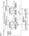
- Fig. 7 illustrates a configuration of a two-symbol collective DCSK demodulation unit 43a in the optical data transmission system according to the second embodiment.
- the two-symbol collective DCSK demodulation unit 43a includes signal sequence extraction circuits 161 and 162, inner product calculation circuits 163a, 163b, 164a and 164b, and adders 165a and 165b.
- the signal sequence extraction circuit 161 extracts sequence corresponding to a reference pseudo-random sequence P0 and signal pseudo-random sequences P1 and P2 from a sub-signal of horizontal polarization.
- the signal sequence extraction circuit 162 extracts sequence corresponding to a reference pseudo-random sequence P0 and signal pseudo-random sequences P1 and P2 from a sub-signal of vertical polarization.
- the inner product calculation circuit 163a calculates an inner product of the reference pseudo-random sequence P0 and the signal pseudo-random sequence P1 extracted from the signal of horizontal polarization to reproduce a first symbol.
- the inner product calculation circuit 163b calculates an inner product of the reference pseudo-random sequence P0 and the signal pseudo-random sequence P2 extracted from the signal of horizontal polarization to reproduce a second symbol.
- the inner product calculation circuit 164a calculates an inner product of the reference pseudo-random sequence P0 and the signal pseudo-random sequence P1 extracted from the signal of vertical polarization to reproduce a first symbol.
- the inner product calculation circuit 164b calculates an inner product of the reference pseudo-random sequence P0 and the signal pseudo-random sequence P2 extracted from the signal of vertical polarization to reproduce a second symbol.
- the adder 165a adds the first symbol obtained from the inner product of the pseudo-random sequences P0 and P1 included in the sub-signal of horizontal polarization and the first symbol obtained from the inner product of the pseudo-random sequences P0 and P1 included in the sub-signal of vertical polarization.
- the adder 165b adds the second symbol obtained from the inner product of the pseudo-random sequences P0 and P2 included in the sub-signal of horizontal polarization and the second symbol obtained from the inner product of the pseudo-random sequences P0 and P2 included in the sub-signal of vertical polarization.
- the first and second symbols are synthesized by the respective additions, and the reliability of the first and second symbols is improved.
- a first symbol is reproduced by calculating an inner product of a reference pseudo-random sequence P0 and a signal pseudo-random sequence P1
- a second symbol is reproduced by calculating an inner product of a reference pseudo-random sequence P0 and a signal pseudo-random sequence P2.
- a reproduced signal of the first symbol is output from the adder 165a
- a reproduced signal of the second symbol is output from the adder 165b.
- a phase offset compensation unit 44 in the second embodiment independently includes phase offset compensation circuits 144a and 144b for a first symbol and a second symbol, as illustrated in Fig. 7 .
- the phase offset compensation circuits 144a and 144b are operated in the same manner as the phase offset compensation unit in the first embodiment.
- the phase offset compensation unit 44 may perform phase offset compensation so as to be operated in cooperation with the first symbol and the second symbol.
- the optical transmitter 10 or the optical receiver 30 in the above-described embodiments may be realized by a computer.
- the optical transmitter 10 or the optical receiver 30 may be realized by recording a program for realizing the function in a computer-readable recording medium and causing a computer system to read and execute the program recorded in the recording medium.
- the "computer system” as mentioned herein includes hardware such as OS and peripheral devices.
- the "computer-readable recording medium” refers to a portable medium such as a flexible disc, a magneto-optical disc, a ROM, or a CD-ROM, or a storage device such as a hard disk built into the computer system.
- the "computer-readable recording medium” may also include a medium dynamically holding the program for a short period of time such as a communication cable used when transmitting the program through a network such as the Internet or through a communication line such as a telephone line as well as a medium holding the program for a fixed period of time such as a volatile memory inside the computer system serving as a server or a client in the above-described case.
- the above-described program may also be for realizing some of the above-described functions, may be realized by combining the above-described functions with a program already recorded in the computer system, or may be realized using a programmable logic device such as a Field-Programmable Gate Array (FPGA).
- FPGA Field-Programmable Gate Array
- the present invention can be applied to applications where it is necessary to suppress an adverse effect to be exerted on a main signal and to multiplex a signal for control with the main signal with high reliability.
Landscapes
- Engineering & Computer Science (AREA)
- Computer Networks & Wireless Communication (AREA)
- Signal Processing (AREA)
- Physics & Mathematics (AREA)
- Electromagnetism (AREA)
- Nonlinear Science (AREA)
- Optical Communication System (AREA)
Abstract
Description
- The present invention relates to a technique of optical communication.
- Priority is claimed on Japanese Patent Application No.
2016-148460, filed July 28, 2016 - With the progress of digital coherent optical transmission techniques in recent years, high-speed and long-distance optical data transmission having a capacity of 100 Gbit/s per wavelength channel has been commercialized. However, research and development on optical data transmission systems having a larger capacity have been actively carried out in order to cope with the increasing demand for network traffic transfer, and an increase of a transmission capacity by multi-valuing and an increase in a baud rate have been proposed.
- In optical data transmission, data communication is performed through an optical fiber. It is necessary to reduce the power of a signal capable of being input to an optical fiber to approximately equal to or less than 10 dBm due to the necessity of avoiding signal distortion due to nonlinear optical effects occurring in an optical fiber. When a transmission capacity is increased by multi-valuing and an increase in a baud rate, energy distributed per bit decreases. For this reason, bit errors easily occur, and a distance over which transmission is possible tends to decrease. In recent years, a communication system which is operable by supporting and switching among a plurality of modulation schemes has also been proposed.
- In a communication system operated by switching among a plurality of modulation schemes, it is necessary to set a modulation scheme and the like between terminals. It is desirable that such a modulation scheme is automatically set, from the viewpoint of improving operability.
- In addition, as another problem, in a large capacity optical transmission channel exceeding 100 Gbit/s, signal processing such as pre-equalization of transmission path frequency characteristics may be performed on a transmission side. In order to perform appropriate signal processing on the transmission side, it is necessary to feedback parameters, such as transmission channel information obtained on a reception side and the quality of a received signal, back to the transmission side.
- In order to realize the above-described automatic setting of a modulation scheme and feedback of parameters for transmission-side signal processing, it is necessary to provide a control channel between terminals. In order to realize automatic setting of a modulation scheme, communication needs to be established prior to connecting of a main signal in the control channel. Further, in order to realize the feedback of parameters for transmission-side signal processing, the control channel needs to provide high reliability even when stable communication cannot be established due to frequent occurrence of errors in a main signal.
- An example in the related art of a control channel satisfying such requirements is disclosed in Patent Literature 1. In the technique disclosed in Patent Literature 1, a waveform in which energy locally exists in a frequency region is used for the transmission of a control signal and is time-multiplexed to a main signal.
- Japanese Unexamined Patent Application, First Publication No.
2014-187525 - However, as disclosed in Patent Literature 1, when a control signal having a signal waveform greatly different from that of a main signal is time-multiplexed to a main signal, there is a risk of causing an adverse effect will be exerted on a signal of an adjacent wavelength channel due to nonlinearity of an optical fiber. In future ultra-large capacity optical data transmission of the 1 Tbit/s class, such adverse effect will not be negligible. For this reason, it is desirable to construct a channel for control using a waveform with characteristics close to those of a main signal.
- In view of the above-described circumstances, an object of the present invention is to provide a technique in which adverse effects are prevented from being exerted on a main signal and in which a signal for control is able to be multiplexed with the main signal with high reliability.
- An optical transmitter in a first aspect of the present invention, which is an optical transmitter of an optical data transmission system transmitting data through an optical fiber transmission path, includes a main signal generator that converts first transmission data into a predetermined signal format to generate a first signal, a Differential Code Shift Keying (DCSK) modulator that DCSK-modulates second transmission data to generate a second signal, a signal-multiplexer that performs time-division multiplexing of the first signal and the second signal, and an electro-optical converter that converts a multiplexed signal obtained by the time-division multiplexing of the signal-multiplexing unit from an electrical signal to an optical signal, and outputs the optical signal to the optical fiber transmission path.
- According to a second aspect of the present invention, the optical transmitter of the first aspect further includes a mapper that maps the second transmission data to a point on a signal space diagram to generate a symbol, the DCSK modulator includes a reference pseudo-random sequence generation circuit that generates a reference pseudo-random sequence, a signal pseudo-random sequence generation circuit that generates a signal pseudo-random sequence, and a time-series signal generator that time-division multiplexes the reference pseudo-random sequence and the signal pseudo-random sequence to generate a single time-series signal as the second signal, and the signal pseudo-random sequence is consistent with a product of the reference pseudo-random sequence and the symbol.
- According to a third aspect of the present invention, the optical transmitter of the first aspect further includes a mapper that maps the second transmission data to a point on a signal space diagram to generate a symbol, the DCSK modulator includes a pseudo-random sequence generator that generates a pseudo-random sequence, a multiplier that multiplies the pseudo-random sequence by the symbol and outputs a multiplication result as a signal pseudo-random sequence, and a time-series signal generator that time-division multiplexes the pseudo-random sequence and the signal pseudo-random sequence to generate a single time-series signal as the second signal.
- An optical receiver in a fourth aspect of the present invention, which is an optical receiver of an optical data transmission system transmitting data through an optical fiber transmission path, includes a photoelectric converter that converts an optical signal received through the optical fiber transmission path into an electric signal, a signal separator that separates a first signal and a second signal from the electric signal, the first and second signals having been time-division multiplexed, a main signal demodulator that demodulates the first signal separated by the signal separator to reproduce first transmission data, and a Differential Code Shift Keying (DCSK) demodulator that DCSK-demodulates the second signal separated by the signal separator to reproduce second transmission data.
- According to a fifth aspect of the present invention, in the optical receiver of the fourth aspect, the DCSK demodulator includes a signal sequence extractor that identifies a reference pseudo-random sequence and a signal pseudo-random sequence and extracts the identified sequences from the second signal and an inner product calculator that calculates an inner product of the reference pseudo-random sequence and the signal pseudo-random sequence and outputs the inner product as the second transmission data.
- An optical data transmission system in a sixth aspect of the present invention includes the optical transmitter according to any one of the first to third aspects and the optical receiver according to the fourth or fifth aspect.
- A transmission method in a seventh aspect of the present invention, which is an optical transmission method performed by an optical transmitter of an optical data transmission system transmitting data through an optical fiber transmission path, includes a main signal generation step of converting first transmission data into a predetermined signal format to generate a first signal, a Differential Code Shift Keying (DCSK) modulation step of DCSK-modulating second transmission data to generate a second signal, a signal-multiplexing step of performing time-division multiplexing of the first signal and the second signal, and an electro-optical conversion step of converting a multiplexed signal obtained by the time-division multiplexing performed in the signal-multiplexing step from an electric signal into an optical signal, and outputting the optical signal to the optical fiber transmission path.
- A reception method in an eighth aspect of the present invention, which is an optical reception method performed by an optical receiver of an optical data transmission system transmitting data through an optical fiber transmission path, includes a photoelectric conversion step of converting an optical signal received through the optical fiber transmission path into an electric signal, a signal separation step of separating a first signal and a second signal from the electric signal, the first and second signals having been time-division multiplexed, a main signal demodulation step of demodulating the first signal separated in the signal separation step to reproduce first transmission data, and a Differential Code Shift Keying (DCSK) demodulation step of DCSK-demodulating the second signal separated in the signal separation step to reproduce second transmission data.
- According to the present invention, it is possible to suppress the adverse effect to be exerted on a main signal and multiplex a signal for control to the main signal with high reliability.
-
-
Fig. 1 is a block diagram illustrating the overall configuration of an optical data transmission system according to a first embodiment of the present invention. -
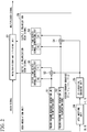
Fig. 2 is a block diagram illustrating a configuration of a DCSK modulation unit according to the first embodiment. -
Fig. 3 is a diagram illustrating a structure of a signal which is time-multiplexed by a main/sub-signal-multiplexing unit in the first embodiment. -
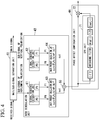
Fig. 4 is a diagram illustrating a configuration of a DCSK demodulation unit in the first embodiment. -
Fig. 5 is a diagram illustrating a configuration of a two-symbol collective DCSK modulation unit in an optical data transmission system according to a second embodiment of the present invention. -
Fig. 6 is a diagram illustrating a structure of a signal which is time-multiplexed in the second embodiment. -
Fig. 7 is a diagram illustrating a configuration of a two-symbol collective DCSK demodulation unit in the second embodiment. -
Fig. 1 is a block diagram illustrating the overall configuration of an optical data transmission system 1 according to a first embodiment of the present invention. The optical data transmission system 1 includes anoptical transmitter 10, anoptical receiver 30 and an opticalfiber transmission path 13 connecting theoptical transmitter 10 and theoptical receiver 30 to each other. Theoptical transmitter 10 includes a transmission-side signal-processing device 11 and an electro-optical conversion device 12. The transmission-side signal-processing device 11 generates a signal to be transmitted at an electric stage. The transmission-side signal-processing device 11 includes a mainsignal generation unit 21, an error correction anddetection encoding unit 22, a synchronouspattern insertion unit 23, a Binary Phase Shift Keying (BPSK)mapping unit 24, adifferential encoding unit 25, a Differential Code Shift Keying (DCSK)modulation unit 26 and a main/sub-signal-multiplexing unit 27. - The main
signal generation unit 21 maps main signal data to a signal in a format appropriate for optical transmission. The error correction anddetection encoding unit 22, the synchronouspattern insertion unit 23, theBPSK mapping unit 24 and thedifferential encoding unit 25 perform error correction encoding, synchronous pattern insertion, BPSK symbol mapping and differential encoding on sub-signal data in this order. TheDCSK modulation unit 26 DCSK-modulates a differentially encoded symbol of the sub-signal data. The main/sub-signal-multiplexing unit 27 performs time-division multiplexing of a main signal (first signal) obtained by mapping the main signal data and a sub-signal (second signal) obtained by DCSK-modulating the differentially encoded symbol of the sub-signal data. The electro-optical conversion device 12 converts a multiplexed signal obtained by performing the time-division multiplexing by the main/sub-signal-multiplexing unit 27 from an electrical signal into an optical signal and transmits the optical signal to theoptical receiver 30 through the opticalfiber transmission path 13. - The
optical receiver 30 includes aphotoelectric conversion device 31 and a reception-side signal-processing device 32. Thephotoelectric conversion device 31 converts the optical signal received through the opticalfiber transmission path 13 into an electric signal. The reception-side signal-processing device 32 reproduces main signal data and sub-signal data from the electric signal at the electric stage. The reception-side signal-processing device 32 includes a main/sub-signal separation unit 41, a mainsignal demodulation unit 42, aDCSK demodulation unit 43, a phaseoffset compensation unit 44, adifferential decoding unit 45, aBPSK demapping unit 46, a synchronous pattern detectionframe synchronization unit 47 and an error correction-decoding unit 48. - The main/
sub-signal separation unit 41 separates the main signal (first signal) and the sub-signal (second signal) having been subjected to time-division multiplexing from the electric signal converted from the optical signal. The mainsignal demodulation unit 42 demodulates the main signal to reproduce the main signal data. TheDCSK demodulation unit 43 DCSK-demodulates the sub-signal separated by the main/sub-signal separation unit 41 to demodulate the symbol of the sub-signal data. The phaseoffset compensation unit 44, thedifferential decoding unit 45, theBPSK demapping unit 46, the synchronous pattern detectionframe synchronization unit 47 and the error correction-decoding unit 48 perform phase offset compensation, differential decoding, BPSK demapping, frame synchronization, and error correction processing on the demodulated symbol of the sub-signal data in this order to reproduce the sub-signal data. - Processing to be performed by the
optical transmitter 10 will be described. InFig. 1 , the main signal data is transmitted to the mainsignal generation unit 21. The mainsignal generation unit 21 maps the main signal data on a signal space diagram in a format (predetermined signal format) appropriate for optical transmission, and transmits a main signal obtained by the mapping to the main/sub-signal-multiplexingunit 27. - Payload data is assumed as the main signal data (first transmission data). In the first embodiment, regarding a main signal, a signal format of polarization multiplexing Quadrature Amplitude Modulation (QAM) is assumed, but other signal formats such as a variable-length code and hybrid modulation may be used. In addition, the main
signal generation unit 21 can use an error correction code for main signal data. - Data for controlling the overall optical data transmission system 1 is assumed as the sub-signal data (second transmission data). The error correction and
detection encoding unit 22 performs error correction encoding on the sub-signal data. The synchronouspattern insertion unit 23 inserts a synchronous pattern into the sub-signal data having been subjected to the error correction encoding. TheBPSK mapping unit 24 maps the sub-signal data having the synchronous pattern inserted thereinto to a symbol on a signal space diagram. Thedifferential encoding unit 25 performs differential encoding on the symbol of the sub-signal data. - Although error correction encoding performed by the error correction and
detection encoding unit 22 is not particularly assumed, it is desirable to install it in the error correction and detection encoding unit from the viewpoint of reliability. As will be described later, the synchronous pattern inserted by the synchronouspattern insertion unit 23 is required for the detection of an error correction block and the like in the reception-side signal-processingdevice 32. Further, in the first embodiment, the phase offsetcompensation unit 44 is included in a circuit on the reception side, and a phase cycle slip may occur on the reception side. For this reason, it is necessary to perform differential encoding, and the differential encoding is performed by thedifferential encoding unit 25. Further, in the first embodiment, BPSK is used as a modulation scheme for the sub-signal data, but Quadrature Phase Shift Keying (QPSK), PSK, QAM, or the like can be used. The speed of modulation for the sub-signal data may be lower than the speed of modulation for the main signal data. - The differentially encoded symbol of the sub-signal data which is obtained by the
differential encoding unit 25 is input to theDCSK modulation unit 26. TheDCSK modulation unit 26 DCSK-modulates the differentially encoded symbol of the sub-signal data. The DCSK modulation is a modulation scheme for loading a signal onto an inner product of a pair of pseudo-random sequences of a reference pseudo-random sequence and a signal pseudo-random sequence. TheDCSK modulation unit 26 outputs a symbol sequence obtained by the DCSK modulation performed on the differentially encoded symbol of the sub-signal data as a sub-signal. In the first embodiment, it is assumed that polarization diversity is performed by performing polarization multiplexing of a signal obtained by DCSK-modulating the differentially encoded symbol of the sub-signal data with a pseudo-random sequence of horizontal polarization and a signal obtained by DCSK-modulating the differentially encoded symbol of the sub-signal data with a pseudo-random sequence of vertical polarization. - The
DCSK modulation unit 26 transmits the sub-signal obtained by performing the DCSK modulation to the main/sub-signal-multiplexingunit 27. The main/sub-signal-multiplexingunit 27 time-division multiplexes the main signal and the sub-signal. The main/sub-signal-multiplexingunit 27 transmits a multiplexed signal obtained by performing the time-division multiplexing to the electro-optical conversion device 12. The electro-optical conversion device 12 converts the multiplexed signal from an electric signal into an optical signal, and outputs the optical signal to the opticalfiber transmission path 13. The optical signal is transmitted to theoptical receiver 30 through the opticalfiber transmission path 13. - The electro-
optical conversion device 12 inputs Continuous Wave (CW) light, an X polarization-side electric signal and a Y polarization-side electric signal so as to be able to cope with polarization multiplexing diversity in two mutually orthogonal polarization directions to generate a polarization-multiplexed optical signal. In a case where a main signal is QAM-modulated and transmitted, the electro-optical conversion device 12 includes an X polarization-side QAM modulator and a Y polarization-side QAM modulator. -
Fig. 2 is a block diagram illustrating a configuration of theDCSK modulation unit 26. TheDCSK modulation unit 26 includes pseudo-randomsequence generation units multipliers signal generation unit 55 and a Y-side time-seriessignal generation unit 56. The pseudo-randomsequence generation units multipliers - The pseudo-random
sequence generation units sequence generation units sequence generation units signal generation unit 21 generates a main signal from main signal data. In order to secure randomness of polarization of an optical signal, the pseudo-randomsequence generation units - The pseudo-random sequence on the X polarization-side from the pseudo-random
sequence generation unit 51 is split into two sequences, which are a reference pseudo-random sequence P0 and a signal pseudo-random sequence P1. The reference pseudo-random sequence P0 is transmitted to the X-side time-seriessignal generation unit 55. The sequence for the signal pseudo-random sequence P1 is transmitted to themultiplier 53. The differentially encoded symbol of the sub-signal data is transmitted to themultiplier 53 from thedifferential encoding unit 25. Themultiplier 53 multiplies the differentially encoded symbol of the sub-signal data by the sequence for the signal pseudo-random sequence P1. Themultiplier 53 transmits a multiplication result to the X-side time-seriessignal generation unit 55 as the signal pseudo-random sequence P1. The X-side time-seriessignal generation unit 55 performs time-division multiplexing of the reference pseudo-random sequence P0 on the X polarization-side and the signal pseudo-random sequence P1 on the X polarization-side to generate a single time-series signal as a DCSK-modulated signal on the X polarization-side. - The pseudo-random sequence on the Y polarization-side from the pseudo-random
sequence generation unit 52 is split into two sequences, which are a reference pseudo-random sequence P0 and a signal pseudo-random sequence P1. The reference pseudo-random sequence P0 is transmitted to the Y-side time-seriessignal generation unit 56. The sequence for the signal pseudo-random sequence P1 is transmitted to themultiplier 54. The differentially encoded symbol of the sub-signal data is transmitted to themultiplier 54 from thedifferential encoding unit 25. Themultiplier 54 multiplies the differentially encoded symbol of the sub-signal data by the sequence for the signal pseudo-random sequence P1 on the Y polarization-side. Themultiplier 54 transmits a multiplication result to the Y-side time-seriessignal generation unit 56 as the signal pseudo-random sequence P1. The Y-side time-seriessignal generation unit 56 performs time-multiplexing of the reference pseudo-random sequence P0 on the Y polarization-side and the signal pseudo-random sequence P1 on the Y polarization-side to generate a single time-series signal as a DCSK-modulated signal on the Y polarization-side. - The DCSK-modulated signal generated by the X-side time-series
signal generation unit 55 and the DCSK-modulated signal generated by the Y-side time-seriessignal generation unit 56 are transmitted to the main/sub-signal-multiplexingunit 27 as sub-signals. Time-division multiplexing of the main signal and the sub-signals is performed by the main/sub-signal-multiplexingunit 27, and a multiplexed signal is generated by the time-division multiplexing. -
Fig. 3 illustrates a structure of a multiplexed signal generated by the main/sub-signal-multiplexingunit 27. A multiplexed signal output from the main/sub-signal-multiplexingunit 27 is divided into periods of main signals and periods of sub-signals, and the main signals and the sub-signals are multiplexed in time division in the respective periods. A DCSK-modulated signal is allocated to the period of the sub-signal. A reference pseudo-random sequence P0 and a signal pseudo-random sequence P1 are allocated to a portion allocated to the sub-signal by time-division multiplexing. A buffer sequence may be inserted between the reference pseudo-random sequence P0 and the signal pseudo-random sequence P1 or before or after the reference pseudo-random sequence P0 and the signal pseudo-random sequence P1. - Processing to be performed by the
optical receiver 30 will be described. An optical signal obtained by multiplexing a main signal and a sub-signal is transmitted to the opticalfiber transmission path 13. In theoptical receiver 30, the optical signal received through the opticalfiber transmission path 13 is converted into an electric signal by thephotoelectric conversion device 31, and the electric signal is input to the reception-side signal-processingdevice 32. - A polarization diversity coherent photoelectric conversion device is assumed as the
photoelectric conversion device 31. For this reason, the optical signal is converted into electric signals of at least two systems corresponding to horizontal polarization and vertical polarization by thephotoelectric conversion device 31. In this case, polarization axes of the horizontal polarization and the vertical polarization are not necessarily consistent with X polarization and Y polarization on the transmission side. In a case where the main signal is QAM-modulated and transmitted, thephotoelectric conversion device 31 includes an X polarization-side QAM demodulator and a Y polarization-side QAM demodulator. - The main/
sub-signal separation unit 41 separates the electric signal input to the reception-side signal-processingdevice 32 into main signals and sub-signals. The mainsignal demodulation unit 42 performs demodulation processing on the main signal. TheDCSK demodulation unit 43 inputs the sub-signal. The main/sub-signal separation unit 41 may separate the main signals and the sub-signals using information regarding a header included in the main signal or the sub-signal. In a case where theoptical transmitter 10 and theoptical receiver 30 are operated in synchronization with each other and frame lengths of main signals and sub-signals in a multiplexed signal are determined in advance, the main/sub-signal separation unit 41 may separate the main signals and the sub-signals at a timing based on the frame lengths determined in advance. - The
DCSK demodulation unit 43 DCSK-demodulates the sub-signal. As described above, time-division multiplexing of the main signal and the sub-signal obtained by performing BPSK mapping, differential encoding, and DCSK modulation in this order on the sub-signal data is performed on the transmission side. Therefore, theDCSK demodulation unit 43 demodulates the sub-signal separated by the main/sub-signal separation unit 41 to acquire a differentially encoded symbol of the sub-signal data. -
Fig. 4 illustrates a configuration of theDCSK demodulation unit 43. TheDCSK demodulation unit 43 includes signalsequence extraction units product calculation units adder 65. - Among the sub-signals separated by the main/
sub-signal separation unit 41, a sub-signal of horizontal polarization is transmitted to the signalsequence extraction unit 61, and a sub-signal of vertical polarization is transmitted to the signalsequence extraction unit 62. The signalsequence extraction unit 61 identifies sequences corresponding to a reference pseudo-random sequence P0 and a signal pseudo-random sequence P1 and extracts the identified sequences from the sub-signal of horizontal polarization. The signalsequence extraction unit 62 identifies sequences corresponding to a reference pseudo-random sequence P0 and a signal pseudo-random sequence P1 and extracts the identified sequences from the sub-signal of vertical polarization. The signalsequence extraction unit 61 may extract the pseudo-random sequences P0 and P1 using information regarding a header included in the sub-signal. In a case where theoptical transmitter 10 and theoptical receiver 30 are operated in synchronization with each other and frame lengths of main signals and sub-signals in a multiplexed signal are determined in advance, the signalsequence extraction unit 61 may extract the pseudo-random sequences P0 and P1 at a timing based on the frame lengths determined in advance. - The signal
sequence extraction unit 61 transmits the extracted reference pseudo-random sequence P0 and signal pseudo-random sequence P1 to the innerproduct calculation unit 63. The signalsequence extraction unit 62 transmits the extracted reference pseudo-random sequence P0 and signal pseudo-random sequence P1 to the innerproduct calculation unit 64. - The inner
product calculation unit 63 calculates an inner product of the reference pseudo-random sequence P0 and the signal pseudo-random sequence P1 which are extracted by the signalsequence extraction unit 61. A symbol of sub-signal data is acquired from a sub-signal of horizontal polarization by calculating the inner product. - The inner
product calculation unit 64 calculates an inner product of the reference pseudo-random sequence P0 and the signal pseudo-random sequence P1 which are extracted by the signalsequence extraction unit 62. A symbol of sub-signal data is acquired from a sub-signal of vertical polarization by calculating the inner product. - The
adder 65 adds an output signal of the innerproduct calculation unit 63 and an output signal of the innerproduct calculation unit 64. Symbols of horizontal polarization and vertical polarization are synthesized by the addition, and thus the reliability of the symbols is improved. Note that the addition is an example of the synthesis of symbols, and symbols may be synthesized using other computation methods. - The
DCSK demodulation unit 43 transmits a symbol of sub-signal data which is obtained by DCSK demodulation to the phase offsetcompensation unit 44. A demodulation output of theDCSK demodulation unit 43 is constituted by a differentially encoded BPSK symbol, but a phase offset may be included therein. The phase offsetcompensation unit 44 compensates for such a phase offset. The phase offsetcompensation unit 44 includes a Carrier Phase Recovery (CPR)unit 71 and amultiplier 72 as illustrated inFig. 4 . TheCPR unit 71 calculates an average of results obtained by squaring each symbol to be input, and calculates a phase of an averaged symbol. A half value of the calculated phase is an estimated value of the phase offset. TheCPR unit 71 outputs a complex number imparting rotation for cancelling out the estimated phase offset. Themultiplier 72 multiplies the complex number output from theCPR unit 71 by the symbol of the sub-signal data to compensate for the phase offset in the symbol of the sub-signal data. - The symbol output by the phase offset
compensation unit 44 is differentially decoded by thedifferential decoding unit 45, and is demodulated to a binary data sequence by theBPSK demapping unit 46. Further, the synchronous pattern detectionframe synchronization unit 47 detects an error correction code block on the basis of a synchronous pattern in the binary data sequence. The error correction-decodingunit 48 decodes the error correction code for the binary data sequence, and thus sub-signal data is reproduced. - As described above, in the optical data transmission system 1 according to the first embodiment of the present invention, an optical signal obtained by performing time-division multiplexing of a sub-signal obtained by DCSK-modulating sub-signal data and a main signal obtained by modulating main signal data is transmitted. The sub-signal data includes data for controlling the overall optical data transmission system 1. That is, the optical data transmission system 1 performs time-division multiplexing of sub-signal data and main signal data modulated using a coherent optical differential encoding modulation scheme (Coherent Optical differential Code Shift Keying: CO-DCSK) and transmits the multiplexed data in order to provide a control channel for transmitting the sub-signal data as data for control. The CO-DCSK scheme is a scheme obtained by extending a DCSK scheme to optical transmission.
- The DCSK-modulated signal is constituted by a set of a reference pseudo-random sequence and a signal pseudo-random sequence, and one symbol is coded by one set. Since light propagating through an optical fiber has two orthogonal polarization states of horizontally polarized light and vertically polarized light, it is possible to improve the quality of a received signal and increase a transmission capacity by performing polarization diversity or polarization multiplexing on the horizontally polarized light and the vertically polarized light in optical data transmission. Note that DCSK modulation is disclosed in, for example, Japanese Patent No.
3995601 optical receiver 30 separates an optical signal in any polarization state into two orthogonal polarization states by coherent detection and converts the separated optical signals into an electric signals. - In the first embodiment, apparent baud rates of reference and signal pseudo-random sequences included in a DCSK-modulated signal are consistent with a baud rate of a main signal. Thereby, a spectrum of a DCSK-modulated signal of a control signal and a spectrum of a main signal are the same as each other. Since a substantial baud rate of sub-signal data in the DCSK-modulated signal is lower than a baud rate of the main signal, noise resistance of the sub-signal data is substantially higher than that of the main signal. Therefore, it is possible to establish communication of a control channel using a sub-signal even in a situation where a main signal is not conducted. In other words, the control channel can have a reliability sufficient to establish communication prior to the main signal.
- In this manner, in the first embodiment, a control channel realized using a sub-signal has higher noise resistance than that of a main signal, and thus it is possible to establish communication prior to the main signal under all circumstances and to transmit information necessary for the establishment of communication of the main signal. The control channel has the same optical power spectrum as an optical power spectrum of the main signal, and also has randomness of a polarization state. A crosstalk of the control channel to an adjacent channel through nonlinearity is the same as a crosstalk of the main signal. Therefore, the optical data transmission system 1 is suitable for improving an optical data transmission system of the related art because it is not necessary to review the design of an optical transmission channel even in a case where time-division multiplexing of the control channel to the main signal is performed. The optical data transmission system 1 can multiplex the sub-signal and the main signal while suppressing the influence on the main signal.
- An optical data transmission system according to a second embodiment of the present invention will be described. The optical data transmission system according to the second embodiment of the present invention is the same as the optical data transmission system 1 according to the first embodiment illustrated in
Fig. 1 as the overall configuration, but there is a difference in configurations of aDCSK modulation unit 26 and aDCSK demodulation unit 43. In the optical data transmission system 1 according to the first embodiment, theDCSK modulation unit 26 and theDCSK demodulation unit 43 perform modulation and demodulation for each symbol. On the other hand, in the optical data transmission system according to the second embodiment, modulation and demodulation of N symbols are collectively performed using N (N is an integer) symbol collective DCSK modulation units and N symbol collective DCSK demodulation units. Note that a case of N=2 will be described in the second embodiment. -
Fig. 5 illustrates a configuration of a two-symbol collectiveDCSK modulation unit 26a in the optical data transmission system according to the second embodiment. The two-symbol collectiveDCSK modulation unit 26a includes pseudo-randomsequence generation units multipliers signal generation unit 155 and a Y-side time-seriessignal generation unit 156. - A pseudo-random sequence on an X polarization-side which is output from the pseudo-random
sequence generation unit 151 is split into a sequence for a reference pseudo-random sequence P0, a sequence for a signal pseudo-random sequence P1 and a sequence for a signal pseudo-random sequence P2. The reference pseudo-random sequence P0 is transmitted to the X-side time-seriessignal generation unit 155. The sequence for the signal pseudo-random sequence P1 is transmitted to themultiplier 153a. The sequence for the signal pseudo-random sequence P2 is transmitted to themultiplier 153b. A differentially encoded symbol (first symbol) of sub-signal data output from thedifferential encoding unit 25 is transmitted to themultiplier 153a. A differentially encoded symbol (second symbol) of sub-signal data to which a delay corresponding to one symbol is added from adelay unit 158 is transmitted to themultiplier 153b. Themultiplier 153a multiplies the first symbol by the sequence for the signal pseudo-random sequence P1, and transmits a multiplication result to the X-side time-seriessignal generation unit 155 as the signal pseudo-random sequence P1. Themultiplier 153b multiplies the second symbol by the sequence for the signal pseudo-random sequence P2, and transmits a multiplication result to the X-side time-seriessignal generation unit 155 as the signal pseudo-random sequence P2. - A pseudo-random sequence on a Y polarization-side which is output from the pseudo-random
sequence generation unit 152 is split into a sequence for a reference pseudo-random sequence P0, a sequence for a signal pseudo-random sequence P1 and a sequence for a signal pseudo-random sequence P2. The reference pseudo-random sequence P0 is transmitted to the Y-side time-seriessignal generation unit 156. The sequence for the signal pseudo-random sequence P1 is transmitted to the multiplier 154a. The sequence for the signal pseudo-random sequence P2 is transmitted to themultiplier 154b. A symbol (first symbol) of sub-signal data which is output from thedifferential encoding unit 25 is transmitted to the multiplier 154a. A symbol (second symbol) of sub-signal data to which a delay corresponding to one symbol is added from thedelay unit 158 is transmitted to themultiplier 154b. The multiplier 154a multiplies the first symbol by the sequence for the signal pseudo-random sequence P1, and transmits a multiplication result to the Y-side time-seriessignal generation unit 156 as the signal pseudo-random sequence P1. Themultiplier 154b multiplies the second symbol by the sequence for the signal pseudo-random sequence P2, and transmits a multiplication result to the Y-side time-seriessignal generation unit 156 as the signal pseudo-random sequence P2. - In the second embodiment, two consecutive symbols in a symbol sequence of sub-signal data are stored in a single sub-signal frame and transmitted. Pseudo-random sequences P0, P1 and P2 on an X polarization-side are generated by the pseudo-random
sequence generation unit 151, themultiplier 153a and themultiplier 153b. Pseudo-random sequences P0, P1 and P2 on a Y polarization-side are generated by the pseudo-randomsequence generation unit 152, the multiplier 154a and themultiplier 154b. Among these, the pseudo-random sequence P0 is a reference pseudo-random sequence, and the pseudo-random sequence P1 is consistent with a product of the reference pseudo-random sequence P0 and the first symbol. The pseudo-random sequence P2 is consistent with a product of the reference pseudo-random sequence P0 and the second symbol. That is, the first symbol is coded into differential information between the reference pseudo-random sequence P0 and the signal pseudo-random sequence P1. The second symbol is coded into differential information between the reference pseudo-random sequence P0 and the signal pseudo-random sequence P2. - The X-side time-series
signal generation unit 155 performs time-division multiplexing of the reference pseudo-random sequence P0, the signal pseudo-random sequence P1 and the signal pseudo-random sequence P2 on the X polarization-side to generate a single time-series signal as a DCSK-modulated signal on the X polarization-side. Similarly, the Y-side time-seriessignal generation unit 156 performs time-division multiplexing of the reference pseudo-random sequence P0, the signal pseudo-random sequence P1 and the signal pseudo-random sequence P2 on the Y polarization-side to generate a single time-series signal as a DCSK-modulated signal on the Y polarization-side. The DCSK-modulated signals on the X polarization-side and the Y polarization-side are transmitted to the main/sub-signal-multiplexingunit 27 as sub-signals. -
Fig. 6 illustrates a structure of a multiplexed signal generated by the main/sub-signal-multiplexingunit 27 in the second embodiment. A multiplexed signal output from the main/sub-signal-multiplexingunit 27 is divided into periods of main signals and periods of sub-signals, and the main signals and the sub-signals are multiplexed in time division in the respective periods. A reference pseudo-random sequence P0, a signal pseudo-random sequence P1 and a signal pseudo-random sequence P2 are allocated to a portion allocated to the sub-signal by time-division multiplexing. A buffer sequence may be inserted among the reference pseudo-random sequence P0 and the signal pseudo-random sequences P1 and P2 or before or after the reference pseudo-random sequence P0 and the signal pseudo-random sequences P1 and P2. -
Fig. 7 illustrates a configuration of a two-symbol collective DCSK demodulation unit 43a in the optical data transmission system according to the second embodiment. The two-symbol collective DCSK demodulation unit 43a includes signalsequence extraction circuits product calculation circuits adders - The signal
sequence extraction circuit 161 extracts sequence corresponding to a reference pseudo-random sequence P0 and signal pseudo-random sequences P1 and P2 from a sub-signal of horizontal polarization. The signalsequence extraction circuit 162 extracts sequence corresponding to a reference pseudo-random sequence P0 and signal pseudo-random sequences P1 and P2 from a sub-signal of vertical polarization. - The inner
product calculation circuit 163a calculates an inner product of the reference pseudo-random sequence P0 and the signal pseudo-random sequence P1 extracted from the signal of horizontal polarization to reproduce a first symbol. The innerproduct calculation circuit 163b calculates an inner product of the reference pseudo-random sequence P0 and the signal pseudo-random sequence P2 extracted from the signal of horizontal polarization to reproduce a second symbol. Similarly, the innerproduct calculation circuit 164a calculates an inner product of the reference pseudo-random sequence P0 and the signal pseudo-random sequence P1 extracted from the signal of vertical polarization to reproduce a first symbol. The innerproduct calculation circuit 164b calculates an inner product of the reference pseudo-random sequence P0 and the signal pseudo-random sequence P2 extracted from the signal of vertical polarization to reproduce a second symbol. - The
adder 165a adds the first symbol obtained from the inner product of the pseudo-random sequences P0 and P1 included in the sub-signal of horizontal polarization and the first symbol obtained from the inner product of the pseudo-random sequences P0 and P1 included in the sub-signal of vertical polarization. Theadder 165b adds the second symbol obtained from the inner product of the pseudo-random sequences P0 and P2 included in the sub-signal of horizontal polarization and the second symbol obtained from the inner product of the pseudo-random sequences P0 and P2 included in the sub-signal of vertical polarization. The first and second symbols are synthesized by the respective additions, and the reliability of the first and second symbols is improved. - In the second embodiment, a first symbol is reproduced by calculating an inner product of a reference pseudo-random sequence P0 and a signal pseudo-random sequence P1, and a second symbol is reproduced by calculating an inner product of a reference pseudo-random sequence P0 and a signal pseudo-random sequence P2. A reproduced signal of the first symbol is output from the
adder 165a, and a reproduced signal of the second symbol is output from theadder 165b. - A phase offset
compensation unit 44 in the second embodiment independently includes phase offsetcompensation circuits Fig. 7 . The phase offsetcompensation circuits compensation unit 44 may perform phase offset compensation so as to be operated in cooperation with the first symbol and the second symbol. - The
optical transmitter 10 or theoptical receiver 30 in the above-described embodiments may be realized by a computer. In this case, theoptical transmitter 10 or theoptical receiver 30 may be realized by recording a program for realizing the function in a computer-readable recording medium and causing a computer system to read and execute the program recorded in the recording medium. Note that the "computer system" as mentioned herein includes hardware such as OS and peripheral devices. In addition, the "computer-readable recording medium" refers to a portable medium such as a flexible disc, a magneto-optical disc, a ROM, or a CD-ROM, or a storage device such as a hard disk built into the computer system. Further, the "computer-readable recording medium" may also include a medium dynamically holding the program for a short period of time such as a communication cable used when transmitting the program through a network such as the Internet or through a communication line such as a telephone line as well as a medium holding the program for a fixed period of time such as a volatile memory inside the computer system serving as a server or a client in the above-described case. The above-described program may also be for realizing some of the above-described functions, may be realized by combining the above-described functions with a program already recorded in the computer system, or may be realized using a programmable logic device such as a Field-Programmable Gate Array (FPGA). - While the embodiments of the present invention have been described above with reference to the accompanying drawings, the specific configuration is not limited to the above-described embodiments and also includes a design and the like without departing from the scope of the present invention.
- The present invention can be applied to applications where it is necessary to suppress an adverse effect to be exerted on a main signal and to multiplex a signal for control with the main signal with high reliability.
-
- 10 Optical transmitter
- 11 Transmission-side signal-processing device
- 12 Electro-optical conversion device
- 13 Optical fiber transmission path
- 21 Main signal generation unit
- 26 DCSK modulation unit
- 27 Main/sub-signal-multiplexing unit
- 30 Optical receiver
- 31 Photoelectric conversion device
- 32 Reception-side signal-processing device
- 41 Main/sub-signal separation unit
- 42 Main signal demodulation unit
- 43 DCSK demodulation unit
- 44 Phase offset compensation unit
- 51, 52 Pseudo-random sequence generation unit
- 53, 54 Multiplier
- 55 X-side time-series signal generation unit
- 56 Y-side time-series signal generation unit
- 61, 62 Signal sequence extraction unit
- 63, 64 Inner product calculation unit
- 65 Adder
Claims (8)
- An optical transmitter of an optical data transmission system transmitting data through an optical fiber transmission path, the optical transmitter comprising:a main signal generator that converts first transmission data into a predetermined signal format to generate a first signal;a Differential Code Shift Keying (DCSK) modulator that DCSK-modulates second transmission data to generate a second signal;a signal-multiplexer that performs time-division multiplexing of the first signal and the second signal; andan electro-optical converter that converts a multiplexed signal obtained by the time-division multiplexing of the signal-multiplexer from an electric signal into an optical signal, and outputs the optical signal to the optical fiber transmission path.
- The optical transmitter according to claim 1, further comprising:a mapper that maps the second transmission data to a point on a signal space diagram to generate a symbol,wherein the DCSK modulator includesa reference pseudo-random sequence generation circuit that generates a reference pseudo-random sequence,a signal pseudo-random sequence generation circuit that generates a signal pseudo-random sequence, anda time-series signal generator that time-division multiplexes the reference pseudo-random sequence and the signal pseudo-random sequence to generate a single time-series signal as the second signal, andwherein the signal pseudo-random sequence is consistent with a product of the reference pseudo-random sequence and the symbol.
- The optical transmitter according to claim 1, further comprising:a mapper that maps the second transmission data to a point on a signal space diagram to generate a symbol,wherein the DCSK modulator includesa pseudo-random sequence generator that generates a pseudo-random sequence,a multiplier that multiplies the pseudo-random sequence by the symbol and outputs a multiplication result as a signal pseudo-random sequence, anda time-series signal generator that time-division multiplexes the pseudo-random sequence and the signal pseudo-random sequence to generate a single time-series signal as the second signal.
- An optical receiver of an optical data transmission system transmitting data through an optical fiber transmission path, the optical receiver comprising:a photoelectric converter that converts an optical signal received through the optical fiber transmission path into an electric signal;a signal separator that separates a first signal and a second signal from the electric signal, the first and second signals having been time-division multiplexed;a main signal demodulator that demodulates the first signal separated by the signal separator to reproduce first transmission data; anda Differential Code Shift Keying (DCSK) demodulator that DCSK-demodulates the second signal separated by the signal separator to reproduce second transmission data.
- The optical receiver according to claim 4, wherein the DCSK demodulator includes:a signal sequence extractor that identifies a reference pseudo-random sequence and a signal pseudo-random sequence and extracts the identified sequences from the second signal; andan inner product calculator that calculates an inner product of the reference pseudo-random sequence and the signal pseudo-random sequence and outputs the inner product as the second transmission data.
- An optical data transmission system comprising:the optical transmitter according to any one of claims 1 to 3; andthe optical receiver according to claim 4 or 5.
- An optical transmission method performed by an optical transmitter of an optical data transmission system transmitting data through an optical fiber transmission path, the optical transmission method comprising:a main signal generation step of converting first transmission data into a predetermined signal format to generate a first signal;a Differential Code Shift Keying (DCSK) modulation step of DCSK-modulating second transmission data to generate a second signal;a signal-multiplexing step of performing time-division multiplexing of the first signal and the second signal; andan electro-optical conversion step of converting a multiplexed signal obtained by the time-division multiplexing performed in the signal-multiplexing step from an electric signal into an optical signal, and outputting the optical signal to the optical fiber transmission path.
- An optical reception method performed by an optical receiver of an optical data transmission system transmitting data through an optical fiber transmission path, the optical reception method comprising:a photoelectric conversion step of converting an optical signal received through the optical fiber transmission path into an electric signal;a signal separation step of separating a first signal and a second signal from the electric signal, the first and second signals having been time-division multiplexed;a main signal demodulation step of demodulating the first signal separated in the signal separation step to reproduce first transmission data; anda Differential Code Shift Keying (DCSK) demodulation step of DCSK-demodulating the second signal separated in the signal separation step to reproduce second transmission data.
Applications Claiming Priority (2)
| Application Number | Priority Date | Filing Date | Title |
|---|---|---|---|
| JP2016148460 | 2016-07-28 | ||
| PCT/JP2017/027031 WO2018021403A1 (en) | 2016-07-28 | 2017-07-26 | Optical transmitter, optical receiver, optical data transmission system, optical transmission method, and optical reception method |
Publications (3)
| Publication Number | Publication Date |
|---|---|
| EP3493429A1 true EP3493429A1 (en) | 2019-06-05 |
| EP3493429A4 EP3493429A4 (en) | 2020-03-25 |
| EP3493429B1 EP3493429B1 (en) | 2021-06-09 |
Family
ID=61016054
Family Applications (1)
| Application Number | Title | Priority Date | Filing Date |
|---|---|---|---|
| EP17834405.7A Active EP3493429B1 (en) | 2016-07-28 | 2017-07-26 | Optical transmitter, optical receiver, optical data transmission system, optical transmission method, and optical reception method |
Country Status (6)
| Country | Link |
|---|---|
| US (1) | US10651944B2 (en) |
| EP (1) | EP3493429B1 (en) |
| JP (1) | JP6626206B2 (en) |
| CN (1) | CN109478928B (en) |
| CA (1) | CA3031607C (en) |
| WO (1) | WO2018021403A1 (en) |
Families Citing this family (5)
| Publication number | Priority date | Publication date | Assignee | Title |
|---|---|---|---|---|
| CN109587090B (en) * | 2019-01-09 | 2021-09-28 | 南京邮电大学 | Three-path carrier index differential chaotic shift keying modem and method |
| US20210399808A1 (en) * | 2020-06-23 | 2021-12-23 | Infinera Corporation | Data synchronization in optical networks and devices |
| CN113411136B (en) * | 2021-06-16 | 2022-11-08 | 广东工业大学 | A quadrature modulation secure optical communication device and method |
| CN118368175B (en) * | 2024-06-17 | 2024-08-16 | 广东工业大学 | Transceiver decoding method and system based on original pattern differential chaotic shift keying |
| CN118677735B (en) * | 2024-08-26 | 2024-11-05 | 南京邮电大学 | Code shift differential chaos shift keying modulation and demodulation method and modulator-demodulator |
Family Cites Families (12)
| Publication number | Priority date | Publication date | Assignee | Title |
|---|---|---|---|---|
| US6616254B1 (en) * | 1997-06-20 | 2003-09-09 | Itran Communications Ltd. | Code shift keying transmitter for use in a spread spectrum communications system |
| US7702245B1 (en) * | 2001-08-15 | 2010-04-20 | Cisco Technology, Inc. | Spread spectrum in-band utility communication channel |
| CA2609877C (en) * | 2005-01-25 | 2015-05-26 | Tir Technology Lp | Method and apparatus for illumination and communication |
| KR100618389B1 (en) | 2005-03-07 | 2006-09-01 | 삼성전자주식회사 | Broadband-DCS modulation method, transmitter using the same, broadband-DCS demodulation method, and receiving device applying the same |
| JP4793765B2 (en) * | 2005-06-28 | 2011-10-12 | 日本電気株式会社 | DPSK modulation / demodulation method, optical communication apparatus and optical communication system using the same |
| KR100757471B1 (en) | 2005-12-08 | 2007-09-11 | 삼성전자주식회사 | Communication system for transmitting / receiving communication signal inserted with IVI |
| JP4826514B2 (en) * | 2007-03-14 | 2011-11-30 | 株式会社日立製作所 | Optical transmission apparatus and control method thereof |
| DE102012211916A1 (en) * | 2012-07-09 | 2014-01-09 | Siemens Aktiengesellschaft | Method and arrangement for transmitting data via an electrical conductor of a power network |
| JP5438856B1 (en) | 2013-03-22 | 2014-03-12 | 日本電信電話株式会社 | Optical transmission / reception system, transmitter, receiver, and optical transmission / reception method |
| JP6240849B2 (en) * | 2013-03-27 | 2017-12-06 | 地方独立行政法人青森県産業技術センター | Safety confirmation system and safety confirmation method |
| JP6371158B2 (en) * | 2013-11-14 | 2018-08-08 | ルネサスエレクトロニクス株式会社 | LED lamp, projector, data processing method, and collision prevention apparatus |
| JP5753604B1 (en) | 2014-03-27 | 2015-07-22 | 日本電信電話株式会社 | Optical transmission / reception system and optical transmission / reception method |
-
2017
- 2017-07-26 CA CA3031607A patent/CA3031607C/en active Active
- 2017-07-26 WO PCT/JP2017/027031 patent/WO2018021403A1/en not_active Ceased
- 2017-07-26 CN CN201780045959.9A patent/CN109478928B/en active Active
- 2017-07-26 JP JP2018530351A patent/JP6626206B2/en active Active
- 2017-07-26 EP EP17834405.7A patent/EP3493429B1/en active Active
- 2017-07-26 US US16/320,065 patent/US10651944B2/en active Active
Also Published As
| Publication number | Publication date |
|---|---|
| JP6626206B2 (en) | 2019-12-25 |
| WO2018021403A1 (en) | 2018-02-01 |
| CN109478928A (en) | 2019-03-15 |
| CN109478928B (en) | 2021-10-08 |
| CA3031607A1 (en) | 2018-02-01 |
| JPWO2018021403A1 (en) | 2018-12-20 |
| US20190273560A1 (en) | 2019-09-05 |
| US10651944B2 (en) | 2020-05-12 |
| CA3031607C (en) | 2021-06-01 |
| EP3493429A4 (en) | 2020-03-25 |
| EP3493429B1 (en) | 2021-06-09 |
Similar Documents
| Publication | Publication Date | Title |
|---|---|---|
| EP3493429B1 (en) | Optical transmitter, optical receiver, optical data transmission system, optical transmission method, and optical reception method | |
| Zhang et al. | Multi-modulus blind equalizations for coherent quadrature duobinary spectrum shaped PM-QPSK digital signal processing | |
| JP5843336B2 (en) | Transmission of multiple asynchronous data streams using higher-order modulation | |
| JP5003391B2 (en) | Optical transmission system and optical transmission method | |
| US8718160B2 (en) | Multi-carrrier optical communication method and system based on DAPSK | |
| US8873953B2 (en) | Multiple-symbol polarization switching for differential-detection modulation formats | |
| CN102577177A (en) | Multi-value modulated light transmitting and receiving device and multi-value modulated light transmitting and receiving method | |
| EP2883314A1 (en) | Methods and apparatus for coherent duobinary shaped pm-qpsk signal processing | |
| JP5753604B1 (en) | Optical transmission / reception system and optical transmission / reception method | |
| JP2016208518A (en) | Signal processing apparatus, signal transmission apparatus and receiver | |
| JP2012010070A (en) | Polarization multiplexed light transmission system, polarization multiplexed light receiver and polarization multiplexed light transmission method | |
| JP6636884B2 (en) | Optical transmitter, optical transmission system and optical receiver | |
| CN113542177B (en) | Method and system for solving frequency offset aliasing of pulse amplitude modulation signal | |
| EP3316500A1 (en) | Optical transmitter, optical receiver, optical transmission system, and optical transmission method | |
| JP5370506B2 (en) | Optical transmission system and optical transmission method | |
| WO2013000746A1 (en) | Method of processing data for optical networks and transmitter for optical networks | |
| JP5813331B2 (en) | Optical receiver | |
| JP7636835B2 (en) | Optical signal demodulation device and optical signal demodulation method | |
| JP7661642B1 (en) | Optical transmitting/receiving device and optical receiver | |
| JP5279959B2 (en) | Parallel differential encoding circuit | |
| JP2014230206A (en) | Transmitter unit, receiver unit, radio communication system, transmission method, reception method and reception program | |
| Nordin et al. | Coherent Optical Communication Systems in Digital Signal Processing | |
| JP2025099182A (en) | Multi-dimensional modulation optical signal demodulation apparatus and optical signal demodulation method | |
| CN114221750A (en) | Safe communication system based on OFDM-PON multi-chaos scrambling | |
| Torres et al. | Characterization and compensation of induced non-linear phase offset in multicarrier optical systems based on clustering techniques |
Legal Events
| Date | Code | Title | Description |
|---|---|---|---|
| STAA | Information on the status of an ep patent application or granted ep patent |
Free format text: STATUS: THE INTERNATIONAL PUBLICATION HAS BEEN MADE |
|
| PUAI | Public reference made under article 153(3) epc to a published international application that has entered the european phase |
Free format text: ORIGINAL CODE: 0009012 |
|
| STAA | Information on the status of an ep patent application or granted ep patent |
Free format text: STATUS: REQUEST FOR EXAMINATION WAS MADE |
|
| 17P | Request for examination filed |
Effective date: 20190121 |
|
| AK | Designated contracting states |
Kind code of ref document: A1 Designated state(s): AL AT BE BG CH CY CZ DE DK EE ES FI FR GB GR HR HU IE IS IT LI LT LU LV MC MK MT NL NO PL PT RO RS SE SI SK SM TR |
|
| AX | Request for extension of the european patent |
Extension state: BA ME |
|
| DAV | Request for validation of the european patent (deleted) | ||
| DAX | Request for extension of the european patent (deleted) | ||
| A4 | Supplementary search report drawn up and despatched |
Effective date: 20200226 |
|
| RIC1 | Information provided on ipc code assigned before grant |
Ipc: H04B 10/2543 20130101ALI20200220BHEP Ipc: H04B 10/077 20130101AFI20200220BHEP Ipc: H04B 10/516 20130101ALI20200220BHEP Ipc: H04B 1/707 20110101ALI20200220BHEP Ipc: H04J 14/08 20060101ALI20200220BHEP Ipc: H04B 10/532 20130101ALI20200220BHEP |
|
| RIC1 | Information provided on ipc code assigned before grant |
Ipc: H04B 1/707 20110101ALI20201127BHEP Ipc: H04B 10/2543 20130101ALI20201127BHEP Ipc: H04B 10/532 20130101ALI20201127BHEP Ipc: H04B 10/077 20130101AFI20201127BHEP Ipc: H04B 10/516 20130101ALI20201127BHEP Ipc: H04J 14/08 20060101ALI20201127BHEP |
|
| GRAP | Despatch of communication of intention to grant a patent |
Free format text: ORIGINAL CODE: EPIDOSNIGR1 |
|
| STAA | Information on the status of an ep patent application or granted ep patent |
Free format text: STATUS: GRANT OF PATENT IS INTENDED |
|
| INTG | Intention to grant announced |
Effective date: 20210114 |
|
| GRAS | Grant fee paid |
Free format text: ORIGINAL CODE: EPIDOSNIGR3 |
|
| GRAA | (expected) grant |
Free format text: ORIGINAL CODE: 0009210 |
|
| STAA | Information on the status of an ep patent application or granted ep patent |
Free format text: STATUS: THE PATENT HAS BEEN GRANTED |
|
| AK | Designated contracting states |
Kind code of ref document: B1 Designated state(s): AL AT BE BG CH CY CZ DE DK EE ES FI FR GB GR HR HU IE IS IT LI LT LU LV MC MK MT NL NO PL PT RO RS SE SI SK SM TR |
|
| REG | Reference to a national code |
Ref country code: GB Ref legal event code: FG4D |
|
| REG | Reference to a national code |
Ref country code: CH Ref legal event code: EP Ref country code: AT Ref legal event code: REF Ref document number: 1401348 Country of ref document: AT Kind code of ref document: T Effective date: 20210615 |
|
| REG | Reference to a national code |
Ref country code: DE Ref legal event code: R096 Ref document number: 602017040139 Country of ref document: DE |
|
| REG | Reference to a national code |
Ref country code: IE Ref legal event code: FG4D |
|
| REG | Reference to a national code |
Ref country code: LT Ref legal event code: MG9D |
|
| PG25 | Lapsed in a contracting state [announced via postgrant information from national office to epo] |
Ref country code: BG Free format text: LAPSE BECAUSE OF FAILURE TO SUBMIT A TRANSLATION OF THE DESCRIPTION OR TO PAY THE FEE WITHIN THE PRESCRIBED TIME-LIMIT Effective date: 20210909 Ref country code: HR Free format text: LAPSE BECAUSE OF FAILURE TO SUBMIT A TRANSLATION OF THE DESCRIPTION OR TO PAY THE FEE WITHIN THE PRESCRIBED TIME-LIMIT Effective date: 20210609 Ref country code: FI Free format text: LAPSE BECAUSE OF FAILURE TO SUBMIT A TRANSLATION OF THE DESCRIPTION OR TO PAY THE FEE WITHIN THE PRESCRIBED TIME-LIMIT Effective date: 20210609 Ref country code: LT Free format text: LAPSE BECAUSE OF FAILURE TO SUBMIT A TRANSLATION OF THE DESCRIPTION OR TO PAY THE FEE WITHIN THE PRESCRIBED TIME-LIMIT Effective date: 20210609 |
|
| REG | Reference to a national code |
Ref country code: AT Ref legal event code: MK05 Ref document number: 1401348 Country of ref document: AT Kind code of ref document: T Effective date: 20210609 |
|
| REG | Reference to a national code |
Ref country code: NL Ref legal event code: MP Effective date: 20210609 |
|
| PG25 | Lapsed in a contracting state [announced via postgrant information from national office to epo] |
Ref country code: NO Free format text: LAPSE BECAUSE OF FAILURE TO SUBMIT A TRANSLATION OF THE DESCRIPTION OR TO PAY THE FEE WITHIN THE PRESCRIBED TIME-LIMIT Effective date: 20210909 Ref country code: LV Free format text: LAPSE BECAUSE OF FAILURE TO SUBMIT A TRANSLATION OF THE DESCRIPTION OR TO PAY THE FEE WITHIN THE PRESCRIBED TIME-LIMIT Effective date: 20210609 Ref country code: RS Free format text: LAPSE BECAUSE OF FAILURE TO SUBMIT A TRANSLATION OF THE DESCRIPTION OR TO PAY THE FEE WITHIN THE PRESCRIBED TIME-LIMIT Effective date: 20210609 Ref country code: SE Free format text: LAPSE BECAUSE OF FAILURE TO SUBMIT A TRANSLATION OF THE DESCRIPTION OR TO PAY THE FEE WITHIN THE PRESCRIBED TIME-LIMIT Effective date: 20210609 Ref country code: GR Free format text: LAPSE BECAUSE OF FAILURE TO SUBMIT A TRANSLATION OF THE DESCRIPTION OR TO PAY THE FEE WITHIN THE PRESCRIBED TIME-LIMIT Effective date: 20210910 |
|
| PG25 | Lapsed in a contracting state [announced via postgrant information from national office to epo] |
Ref country code: ES Free format text: LAPSE BECAUSE OF FAILURE TO SUBMIT A TRANSLATION OF THE DESCRIPTION OR TO PAY THE FEE WITHIN THE PRESCRIBED TIME-LIMIT Effective date: 20210609 Ref country code: SM Free format text: LAPSE BECAUSE OF FAILURE TO SUBMIT A TRANSLATION OF THE DESCRIPTION OR TO PAY THE FEE WITHIN THE PRESCRIBED TIME-LIMIT Effective date: 20210609 Ref country code: SK Free format text: LAPSE BECAUSE OF FAILURE TO SUBMIT A TRANSLATION OF THE DESCRIPTION OR TO PAY THE FEE WITHIN THE PRESCRIBED TIME-LIMIT Effective date: 20210609 Ref country code: EE Free format text: LAPSE BECAUSE OF FAILURE TO SUBMIT A TRANSLATION OF THE DESCRIPTION OR TO PAY THE FEE WITHIN THE PRESCRIBED TIME-LIMIT Effective date: 20210609 Ref country code: CZ Free format text: LAPSE BECAUSE OF FAILURE TO SUBMIT A TRANSLATION OF THE DESCRIPTION OR TO PAY THE FEE WITHIN THE PRESCRIBED TIME-LIMIT Effective date: 20210609 Ref country code: AT Free format text: LAPSE BECAUSE OF FAILURE TO SUBMIT A TRANSLATION OF THE DESCRIPTION OR TO PAY THE FEE WITHIN THE PRESCRIBED TIME-LIMIT Effective date: 20210609 Ref country code: NL Free format text: LAPSE BECAUSE OF FAILURE TO SUBMIT A TRANSLATION OF THE DESCRIPTION OR TO PAY THE FEE WITHIN THE PRESCRIBED TIME-LIMIT Effective date: 20210609 Ref country code: PT Free format text: LAPSE BECAUSE OF FAILURE TO SUBMIT A TRANSLATION OF THE DESCRIPTION OR TO PAY THE FEE WITHIN THE PRESCRIBED TIME-LIMIT Effective date: 20211011 Ref country code: RO Free format text: LAPSE BECAUSE OF FAILURE TO SUBMIT A TRANSLATION OF THE DESCRIPTION OR TO PAY THE FEE WITHIN THE PRESCRIBED TIME-LIMIT Effective date: 20210609 |
|
| PG25 | Lapsed in a contracting state [announced via postgrant information from national office to epo] |
Ref country code: PL Free format text: LAPSE BECAUSE OF FAILURE TO SUBMIT A TRANSLATION OF THE DESCRIPTION OR TO PAY THE FEE WITHIN THE PRESCRIBED TIME-LIMIT Effective date: 20210609 |
|
| REG | Reference to a national code |
Ref country code: CH Ref legal event code: PL |
|
| REG | Reference to a national code |
Ref country code: DE Ref legal event code: R097 Ref document number: 602017040139 Country of ref document: DE |
|
| PG25 | Lapsed in a contracting state [announced via postgrant information from national office to epo] |
Ref country code: MC Free format text: LAPSE BECAUSE OF FAILURE TO SUBMIT A TRANSLATION OF THE DESCRIPTION OR TO PAY THE FEE WITHIN THE PRESCRIBED TIME-LIMIT Effective date: 20210609 |
|
| REG | Reference to a national code |
Ref country code: BE Ref legal event code: MM Effective date: 20210731 |
|
| PLBE | No opposition filed within time limit |
Free format text: ORIGINAL CODE: 0009261 |
|
| STAA | Information on the status of an ep patent application or granted ep patent |
Free format text: STATUS: NO OPPOSITION FILED WITHIN TIME LIMIT |
|
| PG25 | Lapsed in a contracting state [announced via postgrant information from national office to epo] |
Ref country code: LI Free format text: LAPSE BECAUSE OF NON-PAYMENT OF DUE FEES Effective date: 20210731 Ref country code: DK Free format text: LAPSE BECAUSE OF FAILURE TO SUBMIT A TRANSLATION OF THE DESCRIPTION OR TO PAY THE FEE WITHIN THE PRESCRIBED TIME-LIMIT Effective date: 20210609 Ref country code: CH Free format text: LAPSE BECAUSE OF NON-PAYMENT OF DUE FEES Effective date: 20210731 |
|
| 26N | No opposition filed |
Effective date: 20220310 |
|
| PG25 | Lapsed in a contracting state [announced via postgrant information from national office to epo] |
Ref country code: LU Free format text: LAPSE BECAUSE OF NON-PAYMENT OF DUE FEES Effective date: 20210726 Ref country code: AL Free format text: LAPSE BECAUSE OF FAILURE TO SUBMIT A TRANSLATION OF THE DESCRIPTION OR TO PAY THE FEE WITHIN THE PRESCRIBED TIME-LIMIT Effective date: 20210609 |
|
| PG25 | Lapsed in a contracting state [announced via postgrant information from national office to epo] |
Ref country code: IT Free format text: LAPSE BECAUSE OF FAILURE TO SUBMIT A TRANSLATION OF THE DESCRIPTION OR TO PAY THE FEE WITHIN THE PRESCRIBED TIME-LIMIT Effective date: 20210609 Ref country code: IE Free format text: LAPSE BECAUSE OF NON-PAYMENT OF DUE FEES Effective date: 20210726 Ref country code: BE Free format text: LAPSE BECAUSE OF NON-PAYMENT OF DUE FEES Effective date: 20210731 |
|
| PG25 | Lapsed in a contracting state [announced via postgrant information from national office to epo] |
Ref country code: CY Free format text: LAPSE BECAUSE OF FAILURE TO SUBMIT A TRANSLATION OF THE DESCRIPTION OR TO PAY THE FEE WITHIN THE PRESCRIBED TIME-LIMIT Effective date: 20210609 |
|
| PG25 | Lapsed in a contracting state [announced via postgrant information from national office to epo] |
Ref country code: HU Free format text: LAPSE BECAUSE OF FAILURE TO SUBMIT A TRANSLATION OF THE DESCRIPTION OR TO PAY THE FEE WITHIN THE PRESCRIBED TIME-LIMIT; INVALID AB INITIO Effective date: 20170726 |
|
| PG25 | Lapsed in a contracting state [announced via postgrant information from national office to epo] |
Ref country code: MK Free format text: LAPSE BECAUSE OF FAILURE TO SUBMIT A TRANSLATION OF THE DESCRIPTION OR TO PAY THE FEE WITHIN THE PRESCRIBED TIME-LIMIT Effective date: 20210609 |
|
| PG25 | Lapsed in a contracting state [announced via postgrant information from national office to epo] |
Ref country code: MT Free format text: LAPSE BECAUSE OF FAILURE TO SUBMIT A TRANSLATION OF THE DESCRIPTION OR TO PAY THE FEE WITHIN THE PRESCRIBED TIME-LIMIT Effective date: 20210609 |
|
| PGFP | Annual fee paid to national office [announced via postgrant information from national office to epo] |
Ref country code: DE Payment date: 20250722 Year of fee payment: 9 |
|
| PGFP | Annual fee paid to national office [announced via postgrant information from national office to epo] |
Ref country code: GB Payment date: 20250722 Year of fee payment: 9 |
|
| PGFP | Annual fee paid to national office [announced via postgrant information from national office to epo] |
Ref country code: FR Payment date: 20250725 Year of fee payment: 9 |
|
| PG25 | Lapsed in a contracting state [announced via postgrant information from national office to epo] |
Ref country code: TR Free format text: LAPSE BECAUSE OF FAILURE TO SUBMIT A TRANSLATION OF THE DESCRIPTION OR TO PAY THE FEE WITHIN THE PRESCRIBED TIME-LIMIT Effective date: 20210609 |
|
| REG | Reference to a national code |
Ref country code: DE Ref legal event code: R081 Ref document number: 602017040139 Country of ref document: DE Owner name: NTT, INC., JP Free format text: FORMER OWNER: NIPPON TELEGRAPH AND TELEPHONE CORPORATION, TOKYO, JP Ref country code: DE Ref legal event code: R082 Ref document number: 602017040139 Country of ref document: DE Representative=s name: DENNEMEYER & ASSOCIATES RECHTSANWALTSGESELLSCH, DE |