EP3493257A1 - Silicon shielding for baseband termination and rf performance enhancement - Google Patents
Silicon shielding for baseband termination and rf performance enhancement Download PDFInfo
- Publication number
- EP3493257A1 EP3493257A1 EP18209804.6A EP18209804A EP3493257A1 EP 3493257 A1 EP3493257 A1 EP 3493257A1 EP 18209804 A EP18209804 A EP 18209804A EP 3493257 A1 EP3493257 A1 EP 3493257A1
- Authority
- EP
- European Patent Office
- Prior art keywords
- capacitor
- ipd
- electrode
- coupled
- flange
- Prior art date
- Legal status (The legal status is an assumption and is not a legal conclusion. Google has not performed a legal analysis and makes no representation as to the accuracy of the status listed.)
- Granted
Links
Images





Classifications
-
- H—ELECTRICITY
- H03—ELECTRONIC CIRCUITRY
- H03F—AMPLIFIERS
- H03F3/00—Amplifiers with only discharge tubes or only semiconductor devices as amplifying elements
- H03F3/189—High-frequency amplifiers, e.g. radio frequency amplifiers
- H03F3/19—High-frequency amplifiers, e.g. radio frequency amplifiers with semiconductor devices only
- H03F3/193—High-frequency amplifiers, e.g. radio frequency amplifiers with semiconductor devices only with field-effect devices
- H03F3/1935—High-frequency amplifiers, e.g. radio frequency amplifiers with semiconductor devices only with field-effect devices with junction-FET devices
-
- H—ELECTRICITY
- H03—ELECTRONIC CIRCUITRY
- H03F—AMPLIFIERS
- H03F1/00—Details of amplifiers with only discharge tubes, only semiconductor devices or only unspecified devices as amplifying elements
- H03F1/02—Modifications of amplifiers to raise the efficiency, e.g. gliding Class A stages, use of an auxiliary oscillation
- H03F1/0205—Modifications of amplifiers to raise the efficiency, e.g. gliding Class A stages, use of an auxiliary oscillation in transistor amplifiers
-
- H—ELECTRICITY
- H03—ELECTRONIC CIRCUITRY
- H03F—AMPLIFIERS
- H03F1/00—Details of amplifiers with only discharge tubes, only semiconductor devices or only unspecified devices as amplifying elements
- H03F1/56—Modifications of input or output impedances, not otherwise provided for
- H03F1/565—Modifications of input or output impedances, not otherwise provided for using inductive elements
-
- H—ELECTRICITY
- H03—ELECTRONIC CIRCUITRY
- H03F—AMPLIFIERS
- H03F3/00—Amplifiers with only discharge tubes or only semiconductor devices as amplifying elements
- H03F3/189—High-frequency amplifiers, e.g. radio frequency amplifiers
- H03F3/19—High-frequency amplifiers, e.g. radio frequency amplifiers with semiconductor devices only
- H03F3/195—High-frequency amplifiers, e.g. radio frequency amplifiers with semiconductor devices only in integrated circuits
-
- H—ELECTRICITY
- H03—ELECTRONIC CIRCUITRY
- H03F—AMPLIFIERS
- H03F3/00—Amplifiers with only discharge tubes or only semiconductor devices as amplifying elements
- H03F3/20—Power amplifiers, e.g. Class B amplifiers, Class C amplifiers
- H03F3/21—Power amplifiers, e.g. Class B amplifiers, Class C amplifiers with semiconductor devices only
- H03F3/213—Power amplifiers, e.g. Class B amplifiers, Class C amplifiers with semiconductor devices only in integrated circuits
-
- H—ELECTRICITY
- H10—SEMICONDUCTOR DEVICES; ELECTRIC SOLID-STATE DEVICES NOT OTHERWISE PROVIDED FOR
- H10W—GENERIC PACKAGES, INTERCONNECTIONS, CONNECTORS OR OTHER CONSTRUCTIONAL DETAILS OF DEVICES COVERED BY CLASS H10
- H10W42/00—Arrangements for protection of devices
- H10W42/121—Arrangements for protection of devices protecting against mechanical damage
-
- H—ELECTRICITY
- H10—SEMICONDUCTOR DEVICES; ELECTRIC SOLID-STATE DEVICES NOT OTHERWISE PROVIDED FOR
- H10W—GENERIC PACKAGES, INTERCONNECTIONS, CONNECTORS OR OTHER CONSTRUCTIONAL DETAILS OF DEVICES COVERED BY CLASS H10
- H10W44/00—Electrical arrangements for controlling or matching impedance
- H10W44/20—Electrical arrangements for controlling or matching impedance at high-frequency [HF] or radio frequency [RF]
-
- H—ELECTRICITY
- H10—SEMICONDUCTOR DEVICES; ELECTRIC SOLID-STATE DEVICES NOT OTHERWISE PROVIDED FOR
- H10W—GENERIC PACKAGES, INTERCONNECTIONS, CONNECTORS OR OTHER CONSTRUCTIONAL DETAILS OF DEVICES COVERED BY CLASS H10
- H10W76/00—Containers; Fillings or auxiliary members therefor; Seals
- H10W76/10—Containers or parts thereof
- H10W76/12—Containers or parts thereof characterised by their shape
- H10W76/15—Containers comprising an insulating or insulated base
- H10W76/157—Containers comprising an insulating or insulated base having interconnections parallel to the insulating or insulated base
-
- H—ELECTRICITY
- H03—ELECTRONIC CIRCUITRY
- H03F—AMPLIFIERS
- H03F2200/00—Indexing scheme relating to amplifiers
- H03F2200/451—Indexing scheme relating to amplifiers the amplifier being a radio frequency amplifier
-
- H—ELECTRICITY
- H10—SEMICONDUCTOR DEVICES; ELECTRIC SOLID-STATE DEVICES NOT OTHERWISE PROVIDED FOR
- H10W—GENERIC PACKAGES, INTERCONNECTIONS, CONNECTORS OR OTHER CONSTRUCTIONAL DETAILS OF DEVICES COVERED BY CLASS H10
- H10W44/00—Electrical arrangements for controlling or matching impedance
- H10W44/20—Electrical arrangements for controlling or matching impedance at high-frequency [HF] or radio frequency [RF]
- H10W44/203—Electrical connections
- H10W44/206—Wires
-
- H—ELECTRICITY
- H10—SEMICONDUCTOR DEVICES; ELECTRIC SOLID-STATE DEVICES NOT OTHERWISE PROVIDED FOR
- H10W—GENERIC PACKAGES, INTERCONNECTIONS, CONNECTORS OR OTHER CONSTRUCTIONAL DETAILS OF DEVICES COVERED BY CLASS H10
- H10W44/00—Electrical arrangements for controlling or matching impedance
- H10W44/20—Electrical arrangements for controlling or matching impedance at high-frequency [HF] or radio frequency [RF]
- H10W44/203—Electrical connections
- H10W44/209—Vertical interconnections, e.g. vias
-
- H—ELECTRICITY
- H10—SEMICONDUCTOR DEVICES; ELECTRIC SOLID-STATE DEVICES NOT OTHERWISE PROVIDED FOR
- H10W—GENERIC PACKAGES, INTERCONNECTIONS, CONNECTORS OR OTHER CONSTRUCTIONAL DETAILS OF DEVICES COVERED BY CLASS H10
- H10W44/00—Electrical arrangements for controlling or matching impedance
- H10W44/20—Electrical arrangements for controlling or matching impedance at high-frequency [HF] or radio frequency [RF]
- H10W44/226—Electrical arrangements for controlling or matching impedance at high-frequency [HF] or radio frequency [RF] for HF amplifiers
- H10W44/234—Arrangements for impedance matching
-
- H—ELECTRICITY
- H10—SEMICONDUCTOR DEVICES; ELECTRIC SOLID-STATE DEVICES NOT OTHERWISE PROVIDED FOR
- H10W—GENERIC PACKAGES, INTERCONNECTIONS, CONNECTORS OR OTHER CONSTRUCTIONAL DETAILS OF DEVICES COVERED BY CLASS H10
- H10W44/00—Electrical arrangements for controlling or matching impedance
- H10W44/20—Electrical arrangements for controlling or matching impedance at high-frequency [HF] or radio frequency [RF]
- H10W44/241—Electrical arrangements for controlling or matching impedance at high-frequency [HF] or radio frequency [RF] for passive devices or passive elements
-
- H—ELECTRICITY
- H10—SEMICONDUCTOR DEVICES; ELECTRIC SOLID-STATE DEVICES NOT OTHERWISE PROVIDED FOR
- H10W—GENERIC PACKAGES, INTERCONNECTIONS, CONNECTORS OR OTHER CONSTRUCTIONAL DETAILS OF DEVICES COVERED BY CLASS H10
- H10W72/00—Interconnections or connectors in packages
- H10W72/071—Connecting or disconnecting
- H10W72/073—Connecting or disconnecting of die-attach connectors
- H10W72/07331—Connecting techniques
-
- H—ELECTRICITY
- H10—SEMICONDUCTOR DEVICES; ELECTRIC SOLID-STATE DEVICES NOT OTHERWISE PROVIDED FOR
- H10W—GENERIC PACKAGES, INTERCONNECTIONS, CONNECTORS OR OTHER CONSTRUCTIONAL DETAILS OF DEVICES COVERED BY CLASS H10
- H10W72/00—Interconnections or connectors in packages
- H10W72/071—Connecting or disconnecting
- H10W72/073—Connecting or disconnecting of die-attach connectors
- H10W72/07331—Connecting techniques
- H10W72/07336—Soldering or alloying
-
- H—ELECTRICITY
- H10—SEMICONDUCTOR DEVICES; ELECTRIC SOLID-STATE DEVICES NOT OTHERWISE PROVIDED FOR
- H10W—GENERIC PACKAGES, INTERCONNECTIONS, CONNECTORS OR OTHER CONSTRUCTIONAL DETAILS OF DEVICES COVERED BY CLASS H10
- H10W72/00—Interconnections or connectors in packages
- H10W72/071—Connecting or disconnecting
- H10W72/075—Connecting or disconnecting of bond wires
- H10W72/07551—Connecting or disconnecting of bond wires characterised by changes in properties of the bond wires during the connecting
- H10W72/07553—Connecting or disconnecting of bond wires characterised by changes in properties of the bond wires during the connecting changes in shapes
-
- H—ELECTRICITY
- H10—SEMICONDUCTOR DEVICES; ELECTRIC SOLID-STATE DEVICES NOT OTHERWISE PROVIDED FOR
- H10W—GENERIC PACKAGES, INTERCONNECTIONS, CONNECTORS OR OTHER CONSTRUCTIONAL DETAILS OF DEVICES COVERED BY CLASS H10
- H10W72/00—Interconnections or connectors in packages
- H10W72/071—Connecting or disconnecting
- H10W72/075—Connecting or disconnecting of bond wires
- H10W72/07551—Connecting or disconnecting of bond wires characterised by changes in properties of the bond wires during the connecting
- H10W72/07554—Connecting or disconnecting of bond wires characterised by changes in properties of the bond wires during the connecting changes in dispositions
-
- H—ELECTRICITY
- H10—SEMICONDUCTOR DEVICES; ELECTRIC SOLID-STATE DEVICES NOT OTHERWISE PROVIDED FOR
- H10W—GENERIC PACKAGES, INTERCONNECTIONS, CONNECTORS OR OTHER CONSTRUCTIONAL DETAILS OF DEVICES COVERED BY CLASS H10
- H10W72/00—Interconnections or connectors in packages
- H10W72/20—Bump connectors, e.g. solder bumps or copper pillars; Dummy bumps; Thermal bumps
- H10W72/251—Materials
- H10W72/252—Materials comprising solid metals or solid metalloids, e.g. PbSn, Ag or Cu
-
- H—ELECTRICITY
- H10—SEMICONDUCTOR DEVICES; ELECTRIC SOLID-STATE DEVICES NOT OTHERWISE PROVIDED FOR
- H10W—GENERIC PACKAGES, INTERCONNECTIONS, CONNECTORS OR OTHER CONSTRUCTIONAL DETAILS OF DEVICES COVERED BY CLASS H10
- H10W72/00—Interconnections or connectors in packages
- H10W72/30—Die-attach connectors
- H10W72/321—Structures or relative sizes of die-attach connectors
- H10W72/325—Die-attach connectors having a filler embedded in a matrix
-
- H—ELECTRICITY
- H10—SEMICONDUCTOR DEVICES; ELECTRIC SOLID-STATE DEVICES NOT OTHERWISE PROVIDED FOR
- H10W—GENERIC PACKAGES, INTERCONNECTIONS, CONNECTORS OR OTHER CONSTRUCTIONAL DETAILS OF DEVICES COVERED BY CLASS H10
- H10W72/00—Interconnections or connectors in packages
- H10W72/30—Die-attach connectors
- H10W72/351—Materials of die-attach connectors
- H10W72/352—Materials of die-attach connectors comprising metals or metalloids, e.g. solders
-
- H—ELECTRICITY
- H10—SEMICONDUCTOR DEVICES; ELECTRIC SOLID-STATE DEVICES NOT OTHERWISE PROVIDED FOR
- H10W—GENERIC PACKAGES, INTERCONNECTIONS, CONNECTORS OR OTHER CONSTRUCTIONAL DETAILS OF DEVICES COVERED BY CLASS H10
- H10W72/00—Interconnections or connectors in packages
- H10W72/30—Die-attach connectors
- H10W72/351—Materials of die-attach connectors
- H10W72/353—Materials of die-attach connectors not comprising solid metals or solid metalloids, e.g. ceramics
- H10W72/354—Materials of die-attach connectors not comprising solid metals or solid metalloids, e.g. ceramics comprising polymers
-
- H—ELECTRICITY
- H10—SEMICONDUCTOR DEVICES; ELECTRIC SOLID-STATE DEVICES NOT OTHERWISE PROVIDED FOR
- H10W—GENERIC PACKAGES, INTERCONNECTIONS, CONNECTORS OR OTHER CONSTRUCTIONAL DETAILS OF DEVICES COVERED BY CLASS H10
- H10W72/00—Interconnections or connectors in packages
- H10W72/50—Bond wires
- H10W72/531—Shapes of wire connectors
- H10W72/536—Shapes of wire connectors the connected ends being ball-shaped
-
- H—ELECTRICITY
- H10—SEMICONDUCTOR DEVICES; ELECTRIC SOLID-STATE DEVICES NOT OTHERWISE PROVIDED FOR
- H10W—GENERIC PACKAGES, INTERCONNECTIONS, CONNECTORS OR OTHER CONSTRUCTIONAL DETAILS OF DEVICES COVERED BY CLASS H10
- H10W72/00—Interconnections or connectors in packages
- H10W72/50—Bond wires
- H10W72/531—Shapes of wire connectors
- H10W72/537—Multiple bond wires having different shapes
-
- H—ELECTRICITY
- H10—SEMICONDUCTOR DEVICES; ELECTRIC SOLID-STATE DEVICES NOT OTHERWISE PROVIDED FOR
- H10W—GENERIC PACKAGES, INTERCONNECTIONS, CONNECTORS OR OTHER CONSTRUCTIONAL DETAILS OF DEVICES COVERED BY CLASS H10
- H10W72/00—Interconnections or connectors in packages
- H10W72/50—Bond wires
- H10W72/541—Dispositions of bond wires
- H10W72/5445—Dispositions of bond wires being orthogonal to a side surface of the chip, e.g. parallel arrangements
-
- H—ELECTRICITY
- H10—SEMICONDUCTOR DEVICES; ELECTRIC SOLID-STATE DEVICES NOT OTHERWISE PROVIDED FOR
- H10W—GENERIC PACKAGES, INTERCONNECTIONS, CONNECTORS OR OTHER CONSTRUCTIONAL DETAILS OF DEVICES COVERED BY CLASS H10
- H10W72/00—Interconnections or connectors in packages
- H10W72/50—Bond wires
- H10W72/541—Dispositions of bond wires
- H10W72/547—Dispositions of multiple bond wires
- H10W72/5473—Dispositions of multiple bond wires multiple bond wires connected to a common bond pad
-
- H—ELECTRICITY
- H10—SEMICONDUCTOR DEVICES; ELECTRIC SOLID-STATE DEVICES NOT OTHERWISE PROVIDED FOR
- H10W—GENERIC PACKAGES, INTERCONNECTIONS, CONNECTORS OR OTHER CONSTRUCTIONAL DETAILS OF DEVICES COVERED BY CLASS H10
- H10W72/00—Interconnections or connectors in packages
- H10W72/851—Dispositions of multiple connectors or interconnections
- H10W72/874—On different surfaces
- H10W72/884—Die-attach connectors and bond wires
-
- H—ELECTRICITY
- H10—SEMICONDUCTOR DEVICES; ELECTRIC SOLID-STATE DEVICES NOT OTHERWISE PROVIDED FOR
- H10W—GENERIC PACKAGES, INTERCONNECTIONS, CONNECTORS OR OTHER CONSTRUCTIONAL DETAILS OF DEVICES COVERED BY CLASS H10
- H10W90/00—Package configurations
- H10W90/701—Package configurations characterised by the relative positions of pads or connectors relative to package parts
- H10W90/721—Package configurations characterised by the relative positions of pads or connectors relative to package parts of bump connectors
- H10W90/726—Package configurations characterised by the relative positions of pads or connectors relative to package parts of bump connectors between a chip and a stacked lead frame, conducting package substrate or heat sink
-
- H—ELECTRICITY
- H10—SEMICONDUCTOR DEVICES; ELECTRIC SOLID-STATE DEVICES NOT OTHERWISE PROVIDED FOR
- H10W—GENERIC PACKAGES, INTERCONNECTIONS, CONNECTORS OR OTHER CONSTRUCTIONAL DETAILS OF DEVICES COVERED BY CLASS H10
- H10W90/00—Package configurations
- H10W90/701—Package configurations characterised by the relative positions of pads or connectors relative to package parts
- H10W90/731—Package configurations characterised by the relative positions of pads or connectors relative to package parts of die-attach connectors
- H10W90/736—Package configurations characterised by the relative positions of pads or connectors relative to package parts of die-attach connectors between a chip and a stacked lead frame, conducting package substrate or heat sink
-
- H—ELECTRICITY
- H10—SEMICONDUCTOR DEVICES; ELECTRIC SOLID-STATE DEVICES NOT OTHERWISE PROVIDED FOR
- H10W—GENERIC PACKAGES, INTERCONNECTIONS, CONNECTORS OR OTHER CONSTRUCTIONAL DETAILS OF DEVICES COVERED BY CLASS H10
- H10W90/00—Package configurations
- H10W90/701—Package configurations characterised by the relative positions of pads or connectors relative to package parts
- H10W90/751—Package configurations characterised by the relative positions of pads or connectors relative to package parts of bond wires
- H10W90/756—Package configurations characterised by the relative positions of pads or connectors relative to package parts of bond wires between a chip and a stacked lead frame, conducting package substrate or heat sink
-
- H—ELECTRICITY
- H10—SEMICONDUCTOR DEVICES; ELECTRIC SOLID-STATE DEVICES NOT OTHERWISE PROVIDED FOR
- H10W—GENERIC PACKAGES, INTERCONNECTIONS, CONNECTORS OR OTHER CONSTRUCTIONAL DETAILS OF DEVICES COVERED BY CLASS H10
- H10W90/00—Package configurations
- H10W90/701—Package configurations characterised by the relative positions of pads or connectors relative to package parts
- H10W90/751—Package configurations characterised by the relative positions of pads or connectors relative to package parts of bond wires
- H10W90/759—Package configurations characterised by the relative positions of pads or connectors relative to package parts of bond wires between a chip and a laterally-adjacent discrete passive device
Definitions
- Embodiments of the subject matter described herein relate generally to packaged semiconductor devices, and more particularly to packaged radio frequency (RF) amplifiers with shielded integrated passive devices (IPDs).
- RF radio frequency
- IPDs shielded integrated passive devices
- RF transistor devices are commonly used in RF communication infrastructure amplifiers. These RF transistor devices typically include one or more input leads, one or more output leads, one or more transistors, one or more bias leads, and various bondwires coupling the leads to the transistor(s). In some cases, input and output circuits also may be contained within the same package that contains the device's transistor(s).
- an in-package input circuit (e.g., including an input impedance matching circuit) may be coupled between a device's input lead and a control terminal (e.g., the gate) of a transistor
- an in-package output circuit (e.g., including an output impedance matching circuit) may be coupled between a current conducting terminal (e.g., the drain) of a transistor and a device's output lead.
- an RF device's output circuit also may include a baseband decoupling circuit configured to provide an RF ground down to envelope frequencies.
- the ISBW of the device is limited by the low frequency resonance (LFR) caused by interaction between the device's bias feeds and components of such a baseband decoupling circuit.
- LFR low frequency resonance
- RF transistor devices have been developed with limited LFRs in the range of about 450 megahertz (MHz) or less, which supports ISBWs in the range of about 150 MHz or less. Although these devices are sufficient for some applications, the desire for wider RF bandwidth amplifiers continues to increase.
- a conventional RF amplifier device includes an active device (e.g., a transistor), an input impedance matching circuit coupled between an input to the RF amplifier device and an input to the active device, and an output circuit (including an output impedance matching circuit) coupled between an output of the active device and an output of the RF amplifier device.
- an active device e.g., a transistor
- an output circuit including an output impedance matching circuit
- Embodiments of RF amplifier devices discussed herein may also include a baseband decoupling circuit in the output circuit, which is configured to provide an RF ground down to envelope frequencies.
- These RF amplifier device embodiments can include output circuit components that may support wider RF bandwidth amplifiers than are achievable using conventional components, while meeting various performance requirements and other criteria.
- LFR low frequency resonance
- ISBW instantaneous signal bandwidth
- embodiments may enable transmission of signals with a 200 megahertz (MHz) or above ISBW, which corresponds to low LFRs of approximately 600 MHz or greater.
- LFR to ISBW ratio could be from 2.4:1 to 5:1, depending on the system used for linearization (e.g., the digital pre-distortion (DPD) system).
- DPD digital pre-distortion
- a baseband decoupling circuit with a relatively large capacitance value referred to herein as an envelope capacitance or "C env "
- C env envelope capacitance
- Use of low temperature co-fired ceramic (LTCC) structure to integrate baseband decoupling can improve ISBW and help to achieve target LFRs of 1 gigahertz (GHz) and higher.
- the LTCC material used for low frequency decoupling can have losses in carrier frequencies and reduce performance.
- RF shielding in LTCC devices can help enhance performance by reducing eddy currents and controlling the current return path of the RF signals in the packaged transistor, but LTCC shielding may face cost and manufacturing issues in certain devices. As such, RF shielding approaches may be desired for shielding integrated passive devices (IPDs) fabricated using semiconductor-based structures.
- IPDs integrated passive devices
- the transistor and components of the output circuit are mounted on a conductive substrate or flange, and forward current between the transistor and the output lead is carried through bondwires between the transistor and the output lead.
- Reverse current is carried in an opposite direction across the surface of the conductive substrate.
- eddy currents develop during operation in the space between the forward-current-carrying bondwires and the reverse-current-carrying substrate surface.
- the devices may experience significant power loss through the low-Q material at the carrier frequencies.
- embodiments of the inventive subject matter include a current path structure that circumscribes the low-Q material (e.g., dielectric materials included in Cenv), thus substantially reducing or eliminating power losses through that low-Q material.
- the current path structure substantially eliminates the presence of relatively lossy low-Q material between the device's forward and return current paths.
- a "reverse current path structure" is configured to carry reverse current, and it is physically positioned between Cenv and the forward current path.
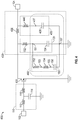
- FIG. 1 is a schematic diagram of an RF amplifier device 100.
- Device 100 includes an input lead 102, an input impedance matching circuit 110, a transistor 120, an output impedance matching circuit 130, an envelope frequency termination circuit 150, and an output lead 104, in an embodiment.
- the output impedance matching circuit 130 and the envelope frequency termination circuit 150 may be referred to collectively as an "output circuit.”
- transistor 120 and various elements of the input and output impedance matching circuits 110, 130 and the envelope frequency termination circuit 150 are shown as singular components, the depiction is for the purpose of ease of explanation only.
- transistor 120 and/or certain elements of the input and output impedance matching circuits 110, 130 and the envelope frequency termination circuit 150 each may be implemented as multiple components (e.g., connected in parallel or in series with each other), and examples of such embodiments are illustrated in the other Figures and described later.
- embodiments may include single-path devices (e.g., including a single input lead, output lead, transistor, etc.), dual-path devices (e.g., including two input leads, output leads, transistors, etc.), and/or multi-path devices (e.g., including two or more input leads, output leads, transistors, etc.).
- the number of input/output leads may not be the same as the number of transistors (e.g., there may be multiple transistors operating in parallel for a given set of input/output leads).
- Input lead 102 and output lead 104 each include a conductor, which is configured to enable the device 100 to be electrically coupled with external circuitry (not shown). More specifically, input and output leads 102, 104 are physically located between the exterior and the interior of the device's package. Input impedance matching circuit 110 is electrically coupled between the input lead 102 and a first terminal of transistor 120, which is also located within the device's interior, and output impedance matching circuit 130 and envelope frequency termination circuit 150 are electrically coupled between a second terminal of transistor 120 and the output lead 104.
- transistor 120 is the primary active component of device 100.
- Transistor 120 includes a control terminal and two current conducting terminals, where the current conducting terminals are spatially and electrically separated by a variable-conductivity channel.
- transistor 120 may be a field effect transistor (FET) (such as a metal oxide semiconductor FET (MOSFET)) or a high electron mobility transistor (HEMT), each of which includes a gate (control terminal), a drain (a first current conducting terminal), and a source (a second current conducting terminal).
- FET field effect transistor
- HEMT high electron mobility transistor
- transistor 120 may be a bipolar junction transistor (BJT).
- references herein to a "gate,” “drain,” and “source,” are not intended to be limiting, as each of these designations has analogous features for a BJT implementation (e.g., a base, collector, and emitter, respectively).
- the gate of transistor 120 is coupled to the input impedance matching circuit 110, the drain of transistor 120 is coupled to the output impedance matching circuit 130 and the envelope frequency termination circuit 150, and the source of transistor 120 is coupled to ground (or another voltage reference).
- the current between the current conducting terminals of transistor 120 may be modulated.
- Input impedance matching circuit 110 is configured to raise the impedance of device 100 to a higher (e.g., intermediate or higher) impedance level (e.g., in a range from about 2 to about 10 Ohms or higher). This can be advantageous in that it allows the printed circuit board level (PCB-level) matching interface from a driver stage to have an impedance that can be achieved in high-volume manufacturing with minimal loss and variation (e.g., a "user friendly" matching interface). Input impedance matching circuit 110 is coupled between the input lead 102 and the control terminal (e.g., gate) of the transistor 120.
- PCB-level printed circuit board level
- input impedance matching circuit 110 is a low pass circuit, which includes two inductive elements 112, 116 (e.g., two sets of bondwires) and a shunt capacitor 114.
- a first inductive element 112 e.g., a first set of bondwires
- a second inductive element 116 e.g., a second set of bondwires
- the second terminal of capacitor 114 is coupled to ground (or another voltage reference).
- the combination of inductive elements 112, 116 and shunt capacitor 114 functions as a low-pass filter.
- the series combination of inductive elements 112, 116 may have a value in a range between about 50 picohenries (pH) to about 3 nanohenries (nH), and shunt capacitor 114 may have a value in a range between about 2 picofarads (pF) to about 100 pF.
- Output impedance matching circuit 130 is configured to match the output impedance of device 100 with the input impedance of an external circuit or component (not shown) that may be coupled to output lead 104. Output impedance matching circuit 130 is coupled between the first current conducting terminal (e.g., drain) of transistor 120 and the output lead 104. According to an embodiment, output impedance matching circuit 130 includes three inductive elements 132, 136, 140 (e.g., three sets of bondwires) and two capacitors 134, 138. Output impedance matching circuit 130 includes a high-pass matching circuit 131 (including inductive element 132 and capacitor 134) and a low-pass matching circuit 135 (including inductive elements 136, 140 and capacitor 138), in an embodiment.
- inductive elements 136, 140 are coupled in series between the first current conducting terminal (e.g., drain) of transistor 120 and the output lead 104, with node 137 between inductive elements 136, 140.
- Capacitor 138 also referred to herein as "CLP” has a first terminal coupled to node 137, and a second terminal coupled to a ground node 157, which in turn may be coupled to ground (or to another voltage reference).
- the combination of inductive elements 136, 140 and capacitor 138 functions as a first (low-pass) matching stage.
- the series combination of inductive elements 136, 140 may have a value in a range between about 40 pH to about 3 nH, and capacitor 138 may have a value in a range between about 2 pF to about 80 pF, although these components may have values outside of these ranges, as well.
- inductive element 132 e.g., a fifth set of bondwires
- Lshunt first current conducting terminal of transistor 120
- capacitor 134 also referred to as "Cshunt”
- a second terminal of capacitor 134 is coupled to a ground node 157.
- the combination of inductive element 132 and capacitor 134 functions as a second (high-pass) matching stage.
- inductive element 132 may have a value in a range between about 80 pH to about 3 nH
- capacitor 134 may have a value in a range between about 50 pF to about 500 pF, although these components may have values outside of these ranges, as well.
- Envelope frequency termination circuit 150 is coupled between the RF cold point (at node 151) and ground node 157, in an embodiment. Envelope frequency termination circuit 150 functions to improve the low frequency resonance of device 100 caused by the interaction between the output impedance matching circuit 130 and the bias feeds by presenting a high impedance at RF frequencies. Envelope frequency termination circuit 150 essentially is "invisible" from a matching standpoint, as it only effects the output impedance at envelope frequencies (i.e., envelope frequency termination circuit 150 provides terminations for the envelope frequencies of device 100).
- envelope frequency termination circuit 150 includes a resistor 152, an inductance 154, and a capacitor 156 coupled in series.
- a first terminal of resistor 152 referred to herein as an “envelope resistor” or “R env ,” is coupled to node 151 (i.e., the RF cold point).
- a second terminal of envelope resistor 152 is coupled to a first terminal of inductance 154, referred to herein as an "envelope inductor” or “L env .”
- a second terminal of inductance 154 is coupled to capacitor 156, referred to herein as an “envelope capacitor” or “C env .”
- a second terminal of the envelope capacitor 156 is coupled to the ground node 157, in an embodiment.
- Envelope resistor 152 may have a value in a range between about 0.1 Ohm to about 2 Ohm, envelope inductance 154 may have a value that is less than about 25 - 500 pH, and envelope capacitor 156 may have a value in a range between about 5 nanofarads (nF) to about 1 microfarad ( ⁇ F), although these components may have values outside of these ranges, as well.
- envelope inductance 154 is shown to include a single lumped element in FIG.
- envelope inductance 154 actually may be made up of one or more distinct inductors (e.g., inductor 754, 854, 1054, FIGs 7 , 8 , 10 ) and additional small inductances associated with other conductive features (e.g., conductive vias and portions of conductive traces) present in the conductive path between RF cold point node 151 and ground node 157.
- inductors e.g., inductor 754, 854, 1054, FIGs 7 , 8 , 10
- additional small inductances associated with other conductive features e.g., conductive vias and portions of conductive traces
- FIG. 2 is a top view of an example of a packaged RF amplifier device 200 that embodies the circuit of FIG. 1 , in accordance with an example embodiment. More particularly, the interconnected electrical components and elements of device 200 may be modeled by the schematic diagram of FIG. 1 . For enhanced understanding, FIG. 2 should be viewed in parallel with FIG. 3 , which is a cross-sectional, side view of the RF amplifier device 200 of FIG. 2 along line 3-3.
- Device 200 includes an input lead 202 (e.g., input lead 102, FIG. 1 ), an output lead 204 (e.g., output lead 104, FIG. 1 ), bias leads 205, a flange 206, an isolation structure 208, and three parallel amplification paths (i.e., three parallel instantiations of circuit 100, FIG. 1 ) electrically coupled between the input and output leads 202, 204.
- Each amplification path includes an input impedance matching circuit 210 (e.g., input impedance matching circuit 110, FIG. 1 ), a transistor 220 (e.g., transistor 120, FIG. 1 ), an output impedance matching circuit 230 (e.g., output impedance matching circuit 130, FIG. 1 ), and an envelope frequency termination circuit 250 (e.g., envelope frequency termination circuit 150, FIG. 1 ).
- Flange 206 includes a rigid electrically-conductive substrate, which has a thickness that is sufficient to provide structural support for other components and elements of device 200.
- flange 206 may function as a heat sink for transistors 220 and other devices mounted on flange 206.
- Flange 206 has a top and bottom surface and a substantially-rectangular perimeter that corresponds to the perimeter of the device 200. In FIG. 2 , only a central portion of the top surface of flange 206 is visible through an opening in isolation structure 208. At least the surface of flange 206 is formed from a layer of conductive material, and possibly all of flange 206 is formed from bulk conductive material. Alternatively, flange 206 may have one or more layers of non-conductive material below its top surface. Either way, flange 206 has a conductive top surface. When device 200 is incorporated into a larger electrical system, flange 206 may be used to provide a ground reference for the device 200.
- Isolation structure 208 has a frame shape, in an embodiment, which includes a substantially enclosed, four-sided structure with a central opening. Isolation structure 208 may have a substantially rectangular shape, as shown in FIG. 2 , or isolation structure 208 may have another shape (e.g., annular ring, oval, and so on). Isolation structure 208 may be formed as a single, integral structure, or isolation structure 208 may be formed as a combination of multiple members. For example, in an alternate embodiment, isolation structure 208 may include multiple portions that contact each other or that are spatially separated from each other (e.g., isolation structure 208 may have one portion isolating input lead 202 from flange 206, and another portion isolating output lead 204 from flange 206). In addition, isolation structure 208 may be formed from a homogenous material, or isolation structure 208 may be formed from multiple layers.
- the input and output leads 202, 204 and the bias leads 205 are mounted on a top surface of the isolation structure 208 on opposed sides of the central opening, and thus the input and output leads 202, 204 and the bias leads 205 are elevated above the top surface of the flange 206, and are electrically isolated from the flange 206.
- the leads 202, 204, 205 may be soldered or otherwise attached to metallization (not shown) on a top surface of isolation structure 208 (e.g., a metallurgic connection).
- the leads 202, 204, 205 are oriented to allow for attachment of bondwires (e.g., bondwires 212, 240) between the leads 202, 204, 205 and components and elements within the central opening of isolation structure 208.
- bondwires e.g., bondwires 212, 240
- bias leads 205 are electrically coupled together with a bar-shaped conductor 207, which also is coupled to the top surface of isolation structure 208.
- conductor 207 includes metallization on a top surface of isolation structure 208. Proximal ends of bias leads 205 are coupled to opposite ends of conductor 207, in an embodiment. Bondwires (not shown) are electrically coupled between conductor 207 and a bias point (e.g., cold point node 151,251, FIGs 1 , 2 ).
- Bias leads 205 extend from the device 200, once packaged, so that their distal ends are exposed and may be coupled to a printed circuit board (PCB) of a larger system to receive a bias voltage. Accordingly, inclusion of bias leads 205 eliminates the need for bias leads on the PCB itself. According to an embodiment, each bias lead 205 has a length corresponding to lambda/4, although each bias lead 205 may have a different length, as well.
- An advantage of including bias leads 205 as part of device 200 is that the bias leads 205 remove the need for quarter wave bias feeds, as additional large value de-coupling capacitors may be connected between the bias leads 205 and ground as the bias leads 205 exit the device package.
- Another embodiment may include a four-lead device with an input lead, an output lead, and two bias leads coupled to the input impedance matching circuit.
- Yet another embodiment includes a six-lead device with an input lead, an output lead, two bias leads coupled to the output impedance matching circuit and two bias leads coupled to the input impedance matching circuit.
- only a single bias lead may be coupled to the input and/or output impedance matching circuits (e.g., particularly for embodiments in which there are more than two RF leads, such as in dual-path and multi-path devices).
- Transistors 220 and various elements 214, 260 of the input and output impedance matching circuits 210, 230 and the envelope frequency termination circuit 250 are mounted on a generally central portion of the top surface of a flange 206 that is exposed through the opening in isolation structure 208.
- the transistors 220 and elements 214, 260 of the input and output impedance matching circuits 210, 230 and the envelope frequency termination circuit 250 may be coupled to flange 206 using conductive epoxy, solder, solder bumps, sintering, and/or eutectic bonds.
- an "active device area” corresponds to a portion of a device on which one or more active devices (e.g., transistor 220) are mounted (e.g., the portion of the conductive surface of flange 206 that exposed through the opening in isolation structure 208).
- Each of transistors 220 has a control terminal (e.g., a gate) and two current conducting terminals (e.g., a drain and a source).
- the control terminal of each transistor 220 is coupled to the input lead 202 through an input impedance matching circuit 210 (e.g., input impedance matching circuit 110, FIG. 1 ).
- one current conducting terminal (e.g., the drain) of each transistor 220 is coupled to the output lead 204 through an output impedance matching circuit 230 (e.g., output impedance matching circuit 130, FIG. 1 ), and the other current conducting terminal (e.g., the source) is coupled to the flange 206 (e.g., to a ground reference node for the device 200).
- each input impedance matching circuit 210 includes two inductive elements 212, 216 (e.g., inductive elements 112, 116, FIG. 1 ) and a capacitor 214 (e.g., capacitor 114, FIG. 1 ).
- Each inductive element 212, 216 is formed from a plurality of parallel, closely-spaced sets of bondwires.
- a first inductive element 212 e.g., inductive element 112, FIG. 1
- a second inductive element 216 e.g., inductive element 116, FIG.
- Capacitor 214 may be, for example, a discrete silicon capacitor (e.g., comprised of a silicon substrate with a top surface corresponding to a first terminal, and a bottom surface corresponding to a second terminal). Bondwires 212, 216 are attached to a conductive top plate at the top surface of capacitor 214.
- each output impedance matching circuit 230 includes three inductive elements 232, 236, 240 (e.g., Lshunt 132, LLP1 136, and LLP2 140, FIG. 1 ) and two capacitors (e.g., Cshunt 134 and CLP 138, FIG. 1 ), where the capacitors form portions of device 260 (e.g., device 160, FIG. 1 ), in an embodiment.
- each inductive element 232, 236, 240 is formed from a plurality of parallel, closely-spaced sets of bondwires.
- shunt inductive element 232 e.g., Lshunt 132, FIG.
- a first series inductive element 236 (e.g., LLP1136, FIG. 1 ) includes a plurality ofbondwires coupled between the first current conducting terminal of transistor 220 and a second bond pad 237 (e.g., corresponding to node 137, FIG.
- the second bond pad 237 is electrically coupled to a low pass matching capacitor (e.g., CLP 138, FIG. 1 ) within the device 260.
- a second series inductive element 240 e.g., LLP2 140, FIG. 1
- Second terminals of the shunt and LP-match capacitors within the device 260 are coupled to the flange 206 (e.g., to ground).
- device 200 is incorporated in an air cavity package, in which transistors 220 and various impedance matching and envelope frequency termination elements are located within an enclosed air cavity 312.
- the air cavity is bounded by flange 206, isolation structure 208, and a cap 310 overlying and in contact with the isolation structure 208 and leads 202, 204.
- a device may be incorporated into an overmolded package (i.e., a package in which the electrical components within the active device area are encapsulated with a non-conductive molding compound, and in which portions of the leads 202, 204 also may be encompassed by the molding compound).
- the output impedance matching circuit 130, 230 includes a high-pass shunt circuit 131 and a low-pass, LP-match circuit 135 (e.g., including inductive elements 136, 140 or bondwires 236, 240 and capacitor 138).
- the low-pass matching circuit 135 may be replaced with a differently-configured matching circuit.
- FIG. 4 is a schematic diagram of an RF amplifier 400 with a second matching circuit 435 (e.g., a low-pass matching circuit with a very high frequency resonance) forming a portion of its output impedance matching circuit 430, in accordance with another example embodiment.
- RF amplifier 400 may be substantially similar to the amplifier 100 of FIG. 1 , and like reference numbers are used in both drawings to indicate elements that may be substantially the same between the two embodiments.
- inductive element 436 is coupled directly between the first current conducting terminal (e.g., drain) of transistor 120 and the output lead 104.
- the high-pass matching circuit 435 which includes a “bond back” or “BB” inductive element 440 coupled in series with a BB capacitor 438, is coupled between the output lead 104 and the ground node 157. More specifically, L BB 440 is coupled between the output lead 104 and a node 437, and CBB 438 is coupled between node 437 and the ground node 157.
- L series 436 may have a value in a range between about 50 pH to about 3 nH
- L BB 440 may have a value in a range between about 50 pH to about 500 pH
- CBB 438 may have a value in a range between about 2 pF to about 50 pF, although these components may have values outside of these ranges, as well.
- FIG. 5 is a top view of an example of a packaged RF amplifier device 500 that embodies the circuit of FIG. 4 , in accordance with an example embodiment. More particularly, the interconnected electrical components and elements of device 500 may be modeled by the schematic diagram of FIG. 4 .
- FIG. 5 should be viewed in parallel with FIG. 6 , which is a cross-sectional, side view of the RF amplifier device 500 of FIG. 5 along line 6-6. Except for the replacement of low-pass matching circuit 135 with low-pass matching circuit 435, and the inclusion of inductive element 436 (e.g., inductive element 536, FIG. 5 ), packaged RF amplifier device 500 may be substantially similar to the device 200 of FIGs 2 and 3 , and like reference numbers are used in both drawings to indicate elements that may be substantially the same between the two embodiments.
- each output impedance matching circuit 530 includes three inductive elements 232, 536, 540 (e.g., L shunt 132, L series 436, and L BB 440, FIG. 4 ) and two capacitors (e.g., C shunt 134 and C BB 438, FIG. 4 ), where the capacitors form portions of device 560 (e.g., device 460, FIG. 4 ), in an embodiment.
- each inductive element 232, 536, 540 is formed from a plurality of parallel, closely-spaced sets of bondwires.
- shunt inductive element 232 e.g., L shunt 132, FIG.
- a fourth inductive element 536 includes a plurality of bondwires coupled between the first current conducting terminal (e.g., the drain) of transistor 220 and a first bond pad 251 (e.g., corresponding to RF cold point node 151, FIG. 4 ) on a top surface of the device 560.
- the first bond pad 251 is electrically coupled to a shunt capacitor (e.g., C shunt 134, FIG. 4 ) within the device 560.
- a series inductive element 536 e.g., L series 436, FIG. 4
- a bond back inductive element 540 includes a plurality of bondwires coupled between the first current conducting terminal of transistor 220 and the output lead 204.
- a bond back inductive element 540 (e.g., L BB 440, FIG.
- a second bond pad 537 (e.g., corresponding to node 437, FIG. 4 ) on the top surface of the device 560.
- the second bond pad 537 is electrically coupled to a bond back capacitor (e.g., CBB 438, FIG. 4 ) within the device 560.
- Second terminals of the shunt and bond back capacitors within the device 560 are coupled to the flange 206 (e.g., to ground).
- a semiconductor (e.g., silicon) integrated passive device (IPD) 701 includes a semiconductor substrate 702 (e.g., a silicon or other semiconductor substrate), a high-density capacitor 756, a first RF (shunt) capacitor 734, and a second RF capacitor 738.
- IPD integrated passive device
- the high-density capacitor 756 corresponds with envelope capacitor 156
- first and second RF capacitors 734 and 738 correspond with capacitors 134 and 138
- active die 720 corresponds with transistor 120
- bondwires 732, 736, and 740 correspond with inductive elements 132, 136, and 140, respectively
- flange 706 corresponds with ground node 157 or flange 206.
- the IPD 701 may comprise a portion of a wafer formed from a bulk semiconductor material, e.g., silicon or another suitable semiconductor material with overlying conductive and dielectric layers.
- the IPD may be formed using a variety of semiconductor processes, including layering dielectric and conductive materials, and patterning the dielectric and conductive material layers, among other processes.
- dielectric and conductive materials can be grown or deposited on the wafer substrate by techniques involving thermal oxidation, nitridation, chemical vapor deposition, evaporation, and sputtering. Photolithography involves the masking of areas of the surface and etching away undesired material to form specific structures.
- the IPD 701 may be fabricated from a number of layers of different materials, including insulators, and conductors that are each patterned to form particular structures within the IPD 701. Such structures may include capacitors, inductors, resistors, transmission lines, and conductive vias that electrically connected different material layers within the IPD 701.
- the wafer may be singulated to separate the IPD 701 from other devices that may be formed in the wafer.
- the IPD 701 can then be connected to other components within an amplifier system.
- the IPD 701 is situated on a flange 706 (e.g., flange 206, FIGs 2 , 3 ), and on opposing sides of IPD 701 are the active die 720 (e.g., die 220, FIGs 2 , 3 ) and portions of the transistor package, such as a portion of the insulator frame 708 (e.g., insulator frame 208, FIGs 2 , 3 ) and an output terminal 704 (e.g., terminal 104 or lead 204, FIGs 1-3 ).
- the active die 720 e.g., die 220, FIGs 2 , 3
- portions of the transistor package such as a portion of the insulator frame 708 (e.g., insulator frame 208, FIGs 2 , 3 ) and an output terminal 704 (e.g., terminal 104 or lead 204, FIGs 1-3 ).
- a terminal of the active die 720 (e.g., a current conducting terminal, such a drain terminal) is connected to a first terminal 733 of the first RF capacitor 734 via a first plurality of bondwires 732, and to a first terminal 737 of the second RF capacitor 738 via a second plurality of bondwires 736.
- the first terminal 733 of the first RF capacitor 734 also is connected, through resistor 752 (e.g., resistor 152, FIG. 1 ) and inductor 754 (e.g., inductor 154, FIG. 1 ) to a first terminal 755 of capacitor 756.
- Second terminals 735, 739, and 757 of the first RF capacitor 734, the second RF capacitor 738, and the high-density capacitor 756 are connected to the flange 706 (e.g., corresponding to node 157, FIG. 1 , and flange 206, FIGs 2 , 3 ).
- the first terminal 737 of the second RF capacitor 738 is connected to the output terminal 704 (e.g., terminal 104 or lead 204, FIGs 1-3 ) via a third plurality of bondwires 740.
- bondwires 732, 736, and 740 correspond with the three inductive elements 132, 136, 140 of FIG. 1 , respectively, and with bondwires 232, 236, 240, FIGs 2 , 3 , respectively.
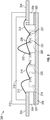
- An electric field in the device 700 is represented by electric field lines 730 extending from the flange 706 to the bondwires 736 and 740.
- a "forward" current I fwd 742 travels from active die 720 along bondwires 736 and 740 and to the output terminal 704.
- a reverse current I rev 744 travels from the output side of the transistor package (e.g., from the portion of insulator frame 708 under output terminal 704) to active die 720 primarily along the flange 706. During operation, the reverse current 744 travels along the surface of the substrate to which IPD 701 is attached (e.g., flange 706, FIG. 7 ).
- the eddy currents develop between the reverse current path 744 and the forward current path 742, and those eddy currents can sometimes impinge upon the material from which high-density capacitor 756 is formed.
- the material from which high-density capacitor 756 may be a relatively-lossy material, and thus those eddy currents may induce significant losses through the material. In other words, during operation, significant loss may occur through the lossy material of high-density capacitor 756, which is positioned between reverse current path 744 and the forward current path 742.
- the first type of loss occurs through the lossy material positioned between the forward current 742 and reverse current 744 paths, as discussed above.
- the second type of loss occurs through additional, relatively lossy material that is positioned very close to the bond pads 737 (e.g., positioned such that the distance ("b") between the lossy material and the bond pad is less than five times the width of bond pad "a").
- the bond pad 737 may behave like a microstrip transmission line. If the lossy material (e.g., a high density capacitor 756) is positioned very physically close to the bond pad 737, the lossy material near the bond pad can decrease the quality factor of the bond pad, potentially leading to significant losses through the lossy material.
- a shielding structure is placed between the material from which the IPD's high-density capacitor is formed and the bond pads of the IPD's RF capacitors, which may allow the high-density capacitor to be positioned closer to bond pads, without incurring the losses that may otherwise be experienced without the shielding structure.
- the dielectric layer of the IPD's second RF capacitor may preferably have a low loss tangent. This can improve the quality factor of the bond pads and may further reduce losses.
- both types of losses are caused by eddy currents in the high density capacitor.
- the first type of loss generally results when the lossy material of the high density capacitor is positioned between reverse current path 744 and the forward current path 742, while the second type of loss generally results when the lossy material of the high density capacitor is positioned very close to bond pad 737, which can behave like a microstrip transmission line.
- RF performance may degrade when using integrated structures like high-density capacitor 756 with semiconductor-based technology because of potential eddy currents being generate within the material of high density capacitor 756. Further, losses from bond pads could reduce drain efficiency in packaged transistors.
- a modified path for the return current which may function as a shielding structure, addresses the performance degradation mentioned above.
- a shielded semiconductor (e.g., silicon) IPD 801 includes a high-density capacitor 856, a first RF (shunt) capacitor 834, and a second RF capacitor 838.
- the high-density capacitor 856 corresponds with envelope capacitor 156
- first and second RF capacitors 834 and 838 correspond with capacitors 134 and 138.
- the IPD 801 is situated on a flange 806 (e.g., corresponding to flange 206, FIGs 2 , 3 ), and on opposing sides of IPD 801 are the active die 820 (e.g., die 220, FIGs 2 , 3 ) and portions of the transistor package, such as a portion of the insulator frame 808 (e.g., insulator frame 208, FIGs 2 , 3 ) and an output terminal 804 (e.g., terminal 104 or lead 204, FIGs 1-3 ).
- the active die 820 e.g., die 220, FIGs 2 , 3
- portions of the transistor package such as a portion of the insulator frame 808 (e.g., insulator frame 208, FIGs 2 , 3 ) and an output terminal 804 (e.g., terminal 104 or lead 204, FIGs 1-3 ).
- a terminal of the active die 820 (e.g., a current conducting terminal, such as a drain terminal) is connected to a first terminal 833 of the first RF capacitor 834 via a first plurality of bondwires 832, and to a first terminal 837 of the second RF capacitor 838 via a second plurality of bondwires 836.
- the first terminal 833 of the first RF capacitor 834 also is connected, through resistor 852 (e.g., resistor 152, FIG. 1 ) and inductor 854 (e.g., inductor 154, FIG. 1 ) to a first terminal 855 of capacitor 856.
- Second terminals (not numbered or shown in FIG.
- first RF capacitor 834 and the second RF capacitor 838 are connected to the flange 806 (e.g., corresponding to node 157, FIG. 1 , and flange 206, FIGs 2 , 3 ).
- the second terminal 857 of the high-density capacitor 856 is connected to the flange 806.
- the first terminal 837 of the second RF capacitor 838 is connected to the output terminal 804 (e.g., terminal 104 or lead 204, FIGs 1-3 ) via a third plurality of bondwires 840.
- bondwires 832, 836, and 840 correspond with the three inductive elements 132, 136, 140 of FIG. 1 , respectively, and with bondwires 232, 236, 240, FIGs 2 , 3 , respectively.
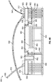
- the shielding structure 848 includes a continuous conductive path, which includes a first vertical portion 849, an elevated horizontal portion 850, and a second vertical portion 851. Ends of the first and second vertical portions 849, 851 of the shielding structure 848 that are proximate to the bottom surface of the IPD 801 are electrically coupled to the flange 806, in an embodiment.
- the elevated horizontal portion 850 is located above the high-density capacitor 856, in an embodiment. Note that in FIG.
- the view depicted shows elevated horizontal portion 850 as two different segments (allowing for the vertical interconnect extending from inductor 854 to high density capacitor 856), but both segments 850 are electrically connected to one another forming a single conductor structure 850 that extends at least from first vertical portion 849 to second vertical portion 851. Accordingly, the materials from which the high-density capacitor 856 is formed are located between the top surface of the flange 806 and the horizontal portion 850 of the shielding structure 848.
- An electric field is represented by electric field lines 830 extending from a first portion of the flange 806 (between active die 820 and the left vertical portion 851 of shielding 848), from the horizontal portion 850 of the shielding structure 848, and from a second portion of the flange (between the right vertical portion 849 of shielding 848 and the insulator frame 808) to the bondwires 836 and 840.
- a "forward" current I fwd 842 travels from the output terminal (e.g., drain terminal) of active die 820 along bondwires 836 and 840 and to the output terminal 804.
- a "return” current I rev 844 travels across the flange 806 from the insulator frame 808, and when it reaches the portion of the flange 806 that is electrically connected to the reverse conductive path structure 848 of the IPD 801 (or more specifically to vertical portion 849), significant portions of the reverse current 844 travel from the flange 806 at the right side of the IPD 801 into and through the reverse conductive path structure 848 to the flange 806 at the left side of the IPD 801, rather than traveling along the portion of the surface of the flange 806 to which IPD 801 is attached (e.g., the portion of flange 806 underlying the reverse conductive path structure 848 and between the vertical portions 849, 851 of the reverse conductive path structure 848).
- the reverse current path structure 848 substantially reduces or eliminates the presence of relatively lossy material for the high-density capacitor 856 between the device's forward path 842 and the portion of the return current path 844 that is carried by the reverse current path structure 848.
- FIGS. 9A and 9B An exemplary implementation of shielded device 800 is depicted by device 900 in FIGS. 9A and 9B .
- FIGS. 9A and 9B of device 900 are each cross-sectional views of device 900 taken through different portions of device 900.
- Device 900 includes a conductive layer 906 (e.g., which may be coupled to a flange 806) deposited on a surface of a semiconductor substrate 803 (e.g., a silicon or other semiconductor substrate), and a plurality of conductive and dielectric layers formed on or over the top surface of the semiconductor substrate 803.
- a conductive layer 906 e.g., which may be coupled to a flange 806
- a semiconductor substrate 803 e.g., a silicon or other semiconductor substrate
- a plurality of conductive and dielectric layers formed on or over the top surface of the semiconductor substrate 803.
- Z-heights can vary greatly depending on the application, but example Z-heights, for certain implementations, may be, for example, 74 microns ( ⁇ m) for Z-height 962, 77 ⁇ m for Z-height 964, and 81 ⁇ m for Z-height 966.
- disposed is intended to identify relative position, and does not signify “placement” of the layer during a manufacturing process, or require direct contact between the layers disposed on top of each other (i.e., there could be additional layers or structures in between one layer disposed on another layer).
- the conductive layers may be deposited and patterned to have different structures and shapes by etching. It is noted that device 900 includes other layers not illustrated in FIGs. 9A and 9B , and that the representations in FIGs. 9A and 9B are not to scale.
- Device 900 includes first and second RF capacitors 834, 838, and high-density capacitor 856.
- the high-density capacitor 856 may include terminals 855, 857 (or electrodes) patterned into the first and third conductive layers 982, 986, and the terminals may be separated by a portion of a dielectric layer 859, although capacitor 856 may be implemented in other ways (e.g., using other conductive layers).
- capacitor 856 may be a MIM (metal-insulator-metal) capacitor that is integrally formed as a portion of the device 900.
- MIM metal-insulator-metal
- the capacitor 856 may be formed entirely above the semiconductor substrate 803, or may have portions that extend into the semiconductor substrate 803 or are otherwise coupled to, or in contact with, semiconductor substrate 803. According to an embodiment, the capacitor 856 may be formed from a first electrode 855, a second electrode 857, and a dielectric material 859 between the first and third electrodes.
- the dielectric material 859 of capacitor 856 may include one or more layers of polysilicon, various oxides, a nitride, or other suitable materials.
- the first and second electrodes 855, 857 may include horizontal portions of conductive layers (e.g., portions that are parallel to portion 950) and/or vertical portions (e.g., portions that are orthogonal to portion 950) of conductive layers that are interconnected. Further, the first and second electrodes 855, 857 may be formed from metal layers and/or from conductive semiconductor materials (e.g., polysilicon). Although particular two-plate capacitor structures are shown in FIGs 8-9 , a variety of other capacitor structures alternatively may be utilized, as would be understood by one of skill in the art based on the description herein.
- the third metal layer 986 includes a first portion 907, which may form a first terminal (or electrode) of RF capacitor 834, and a second portion 912, which may form a first terminal (or electrode) of RF capacitor 838.
- the first terminals of capacitors 834, 838 may be formed from different conductive layers.
- a portion 950 of a conductive layer (e.g., the third conductive layer 986) is disposed over high-density capacitor 856 to elevate the return current path over the high-density capacitor 856.
- first, second, and third conductive features 907, 912, and 950 are depicted as being formed from portions of the third conductive layer 986, and thus are depicted at the same height (i.e., height 966), they are not continuous, but rather separate segments of the third conductive layer 986. In other embodiments, conductive features 907, 912, and 950 may be formed from portions of different conductive layers.
- TSVs 952, 954 extend from the bottom surface of IPD 801 (and thus from flange 806) to the horizontal shielding portion 950 of the third conductive layer 986.
- the reverse current I rev 844 is provided with a conductive current path 848 (see arrows 954 in FIG. 9B ) over the high-density capacitor 856 via the TSVs 952, 954 and shielding portion 950.
- TSVs 954 correspond to the first vertical portion 849
- a patterned portion of layer 966 corresponds to an elevated horizontal portion 850
- the second vertical portion 851 corresponds to TSVs 952.
- FIG. 10 depicts a top view of a shielded IPD 1000 that can be used to implement the approach represented in FIGs. 9A and 9B .
- the shielded IPD 1000 includes first RF capacitor 1034 (e.g., capacitor 134, 834, FIGs 1 , 9B ), a plurality of parallel-coupled second RF capacitors 1038 (e.g., capacitor 138, 838, FIGs 1 , 9B ), a resistor 1052 (e.g., resistor 152, 852, FIGs 1 , 9B ), parallel inductors 1054 (e.g., inductor 154, 854, FIGs 1 , 9A ), and a buried high-density capacitor (e.g., capacitor 156, 856, FIGs 1 , 9B ), which is not visible in the top view of FIG. 10 .
- the various components are interconnected as previously described.
- shielding structure 1050 Near the center is shielding structure 1050, which may be formed at least in part by, for example, the shielding portion 950 of third conductive layer 986. It is noted that the horizontal portion of the shielding structure 1050 needs not be limited to only the third conductive layer 986, and may alternatively or additionally include portions of other layers, such as the second conductive layer 984, or other conductive layers. Further, an embodiment of a device may include more than three conductive layers, and the horizontal portion of the shielding structure 1050 may be formed from various portions of those layers.
- the high-density capacitor within the IPD 1000 is not viewable from the top (in the top view of FIG. 10 ) because it is positioned underneath the horizontal portion of shielding structure 1050.
- RF capacitor 1034 (corresponding with capacitor 134 in FIG. 1 or 834 in FIG. 9B ), and RF capacitor 1038 (corresponding with capacitor 138 in FIG. 1 or 838 in FIG. 9B ).
- An inductive element 1054 (corresponding with inductance 154 in FIG. 1 or 854 in FIG. 9A ), and a resistor 1052 (corresponding with resistor 152 in FIG. 1 or 852 in FIG. 9B ), are also depicted in this top-view perspective. In actuality, some or all of these components may be buried under overlying layers.
- the shielding structure 1050 may include a plurality of slots (voids) 1080 that may help to prevent die crack and decrease warpage.
- the slot size may be, for example, about 2-6 microns ( ⁇ m) wide (e.g., 5 ⁇ m) by about 300-600 ⁇ m long (e.g., 545 ⁇ m) for IPD arrangements in example implementations.
- the length and width dimensions of slot 1080 may be, for example, no larger than about one tenth of the wavelength of the low end of operating frequency.
- a plurality of conductive vias 1053, 1055 may make up the vertical portions of the shielding structure (e.g., vertical portions 849, 851, FIG. 8 , or TSVs 952, 954, FIG. 9B ).
- the vertical portions of the shielding structure may include a row of aligned vias 1053, 1055, in some embodiments.
- each via may have a length 1060 in a range of about 1 ⁇ m to about 50 ⁇ m, and a width 1062 in a range of about 1 ⁇ m to about 50 ⁇ m.
- the vias 1053, 1055 may be circular, oval, or may have some other cross-sectional shape.
- vias may be arranged in different manners, in other embodiments. Having multiple vias in parallel can reduce the impedance of the vias to enable the device to operate more efficiently. It is noted that some of the vias may be interconnected while others may be isolated. Also, vias may extend up to different layers (e.g., the second conductive layer 984 or the third conductive layer 986, depicted in FIGs. 9A and 9B ). The number and configuration of vias may be driven at least in part by the internal circuitry in a package, and other interconnections and configurations may be utilized to suit different applications in other embodiments.
- Low-frequency probe testing for baseband has shown that the LFR is over 850 MHz using a high-density capacitor, as compared with LFRs of about 85 MHz in designs without a baseband termination circuit.
- the shielding structure is not expected to deteriorate baseband performance.
- the embodiments discussed above are well-suited for many RF power products, including but not limited to those that require ISBWs greater than 200 MHz with reduced power dissipation (that may result from electromagnetic coupling) and high RF efficiency.
- the disclosed approach helps enable multiband transistors in discrete, integrated circuit (IC), or module format.
- Products can be, for example, in air cavity or overmolded packages, and may be single-stage or multi-stage products.
- Example implementations can be directly incorporated into, for example, transistor products based on silicon (Si), gallium arsenide (GaAs), and/or gallium nitride (GaN).
- an IPD includes a semiconductor substrate and a MIM capacitor coupled to the semiconductor substrate.
- the MIM capacitor includes a first electrode, a second electrode, and a dielectric between the first electrode and the second electrode.
- the IPD includes a first RF capacitor over the semiconductor substrate, a second RF capacitor over the semiconductor substrate, and a metal layer patterned to form a portion of an elevated metal shielding structure.
- the elevated metal shielding structure is over the MIM capacitor.
- At least one of the first electrode and the second electrode of the MIM capacitor includes a first portion that is parallel to the elevated metal shielding structure and a second portion that is orthogonal to the elevated metal shielding structure.
- the further comprises a via through the semiconductor substrate.
- the via is electrically coupled to the elevated metal shielding structure.
- At least one of the first electrode and the second electrode of the MIM capacitor includes a conductive semiconductor material.
- the metal layer is patterned to form a first plate of the first RF capacitor and a first plate of the second RF capacitor.
- the IPD further includes a set of slots formed in the elevated metal shielding structure.
- Each slot has a width ranging from 0.1 ⁇ m to 10000 ⁇ m and a length ranging from 0.1 ⁇ m to 10000 ⁇ m.
- the dielectric includes one or more layers of a polysilicon material, an oxide material, or a nitride material.
- an RF amplifier device includes a ground flange, a semiconductor die on the ground flange and an IPD on the ground flange.
- the IPD includes a semiconductor substrate, a MIM capacitor coupled to the semiconductor substrate, a first RF capacitor over the semiconductor substrate, a second RF capacitor over the semiconductor substrate, and a metal layer patterned to form a portion of an elevated metal shielding structure.
- the elevated metal shielding structure is over the MIM capacitor.
- the IPD is electrically coupled to the semiconductor die.
- the MIM capacitor is part of an envelope frequency termination circuit of the RF amplifier device.
- the first RF capacitor and the second RF capacitor are part of an output impedance matching circuit of the RF amplifier device.
- the MIM capacitor includes a first electrode, a second electrode, and a dielectric between the first electrode and the second electrode. At least one of the first electrode and the second electrode of the MIM capacitor includes a first portion that is parallel to the elevated metal shielding structure and a second portion that is orthogonal to the elevated metal shielding structure.
- the RF amplifier device further comprises a via through the semiconductor substrate.
- the via is electrically coupled to the elevated metal shielding structure.
- the MIM capacitor includes a first electrode, a second electrode, and a dielectric between the first electrode and the second electrode. At least one of the first electrode and the second electrode of the MIM capacitor includes a conductive semiconductor material.
- the dielectric includes one or more layers of a polysilicon material, an oxide material, or a nitride material.
- the metal layer is patterned to form a first plate of the first RF capacitor and a first plate of the second RF capacitor.
- the RF amplifier further includes a set of slots formed in the elevated metal shielding structure.
- Each slot having a width ranging from 0.1 ⁇ m to 10000 ⁇ m and a length ranging from 0.1 ⁇ m to 10000 ⁇ m.
- an RF amplifier device includes a ground flange, a semiconductor die on the ground flange, and an IPD on the ground flange.
- the IPD includes a semiconductor substrate and a MIM capacitor coupled to the semiconductor substrate.
- the MIM capacitor includes a first electrode, a second electrode, and a dielectric between the first electrode and the second electrode.
- the RF amplifier device includes a first RF capacitor over the semiconductor substrate, a second RF capacitor over the semiconductor substrate, and a metal layer patterned to form a portion of an elevated metal shielding structure, a first plate of the first RF capacitor and a first plate of the second RF capacitor.
- the elevated metal shielding structure is over the MIM capacitor.
- the IPD is electrically coupled to the semiconductor die. At least one of the first electrode and the second electrode of the MIM capacitor includes a first portion that is parallel to the elevated metal shielding structure and a second portion that is orthogonal to the elevated metal shielding structure.
- the first RF capacitor and the second RF capacitor are part of an output impedance matching circuit of the RF amplifier device.
- At least one of the first electrode and the second electrode of the MIM capacitor includes a conductive semiconductor material.
- the dielectric includes one or more layers of a polysilicon material, an oxide material, or a nitride material.
- node means any internal or external reference point, connection point, junction, signal line, conductive element, or the like, at which a given signal, logic level, voltage, data pattern, current, or quantity is present.
- two or more nodes may be realized by one physical element (and two or more signals can be multiplexed, modulated, or otherwise distinguished even though received or output at a common node).
Landscapes
- Engineering & Computer Science (AREA)
- Power Engineering (AREA)
- Microelectronics & Electronic Packaging (AREA)
- Amplifiers (AREA)
- Microwave Amplifiers (AREA)
Abstract
Description
- Embodiments of the subject matter described herein relate generally to packaged semiconductor devices, and more particularly to packaged radio frequency (RF) amplifiers with shielded integrated passive devices (IPDs).
- High power, radio frequency (RF) transistor devices are commonly used in RF communication infrastructure amplifiers. These RF transistor devices typically include one or more input leads, one or more output leads, one or more transistors, one or more bias leads, and various bondwires coupling the leads to the transistor(s). In some cases, input and output circuits also may be contained within the same package that contains the device's transistor(s). More specifically, an in-package input circuit (e.g., including an input impedance matching circuit) may be coupled between a device's input lead and a control terminal (e.g., the gate) of a transistor, and an in-package output circuit (e.g., including an output impedance matching circuit) may be coupled between a current conducting terminal (e.g., the drain) of a transistor and a device's output lead.
- Instantaneous signal bandwidth (ISBW) is becoming a major requirement for RF communication infrastructure amplifiers, and thus for the high-power RF transistor devices included in such amplifiers. Along with an impedance matching circuit, an RF device's output circuit also may include a baseband decoupling circuit configured to provide an RF ground down to envelope frequencies. Generally, the ISBW of the device is limited by the low frequency resonance (LFR) caused by interaction between the device's bias feeds and components of such a baseband decoupling circuit. In recent years, RF transistor devices have been developed with limited LFRs in the range of about 450 megahertz (MHz) or less, which supports ISBWs in the range of about 150 MHz or less. Although these devices are sufficient for some applications, the desire for wider RF bandwidth amplifiers continues to increase.
- A more complete understanding of the subject matter may be derived by referring to the detailed description and claims when considered in conjunction with the following figures, wherein like reference numbers refer to similar elements throughout the figures.
-
FIG. 1 is a schematic diagram of an RF amplifier with input and output circuits, in accordance with an example embodiment; -
FIG. 2 is a top view of an example of a packaged RF amplifier device that embodies the circuit ofFIG. 1 , in accordance with an example embodiment; -
FIG. 3 is a cross-sectional, side view of the RF amplifier device ofFIG. 2 along line 3-3; -
FIG. 4 is a schematic diagram of an RF amplifier with input and output circuits, in accordance with another example embodiment; -
FIG. 5 is a top view of an example of a packaged RF amplifier device that embodies the circuit ofFIG. 4 , in accordance with an example embodiment; -
FIG. 6 is a cross-sectional, side view of the RF amplifier device ofFIG. 5 along line 6-6; -
FIG. 7 is a cross-sectional, simplified side view of an RF amplifier device with an unshielded integrated passive device (IPD) that includes a high-density capacitor, showing forward and reverse current paths; -
FIG. 8 is a cross-sectional, simplified side view of an RF amplifier device with a shielded IPD that includes a high-density capacitor, showing forward and reverse current paths, in accordance with one or more example embodiments; -
FIG. 9A is a cross-sectional, more-detailed side view, alongline 9A-9A shown inFIG. 10 , of an RF amplifier device with a shielded IPD that includes a high-density capacitor, showing metal layers and through-silicon vias (TSVs), in accordance with one or more example embodiments; -
FIG. 9B is a cross-sectional, more-detailed side view, alongline 9B-9B shown inFIG. 10 , of an RF amplifier device with a shielded IPD that includes a high-density capacitor, showing metal layers, TSVs, and forward and reverse current paths, in accordance with one or more example embodiments; and -
FIG. 10 is a top view of an example shielded IPD of a packaged RF amplifier device, such as the one depicted inFIGs. 9A and9B , in accordance with one or more example embodiments. - A conventional RF amplifier device includes an active device (e.g., a transistor), an input impedance matching circuit coupled between an input to the RF amplifier device and an input to the active device, and an output circuit (including an output impedance matching circuit) coupled between an output of the active device and an output of the RF amplifier device. Embodiments of RF amplifier devices discussed herein may also include a baseband decoupling circuit in the output circuit, which is configured to provide an RF ground down to envelope frequencies. These RF amplifier device embodiments can include output circuit components that may support wider RF bandwidth amplifiers than are achievable using conventional components, while meeting various performance requirements and other criteria. For example, assuming a 3:1 ratio of low frequency resonance (LFR) to instantaneous signal bandwidth (ISBW), embodiments may enable transmission of signals with a 200 megahertz (MHz) or above ISBW, which corresponds to low LFRs of approximately 600 MHz or greater. In other cases, the LFR to ISBW ratio could be from 2.4:1 to 5:1, depending on the system used for linearization (e.g., the digital pre-distortion (DPD) system).
- In various embodiments, a baseband decoupling circuit with a relatively large capacitance value, referred to herein as an envelope capacitance or "Cenv", is used to achieve an increased LFR (and thus increased ISBW). Use of low temperature co-fired ceramic (LTCC) structure to integrate baseband decoupling can improve ISBW and help to achieve target LFRs of 1 gigahertz (GHz) and higher. However, in certain applications, the LTCC material used for low frequency decoupling can have losses in carrier frequencies and reduce performance. RF shielding in LTCC devices can help enhance performance by reducing eddy currents and controlling the current return path of the RF signals in the packaged transistor, but LTCC shielding may face cost and manufacturing issues in certain devices. As such, RF shielding approaches may be desired for shielding integrated passive devices (IPDs) fabricated using semiconductor-based structures.
- In a conventional high-power RF transistor device, the transistor and components of the output circuit are mounted on a conductive substrate or flange, and forward current between the transistor and the output lead is carried through bondwires between the transistor and the output lead. Reverse current, on the other hand, is carried in an opposite direction across the surface of the conductive substrate. In this configuration, eddy currents develop during operation in the space between the forward-current-carrying bondwires and the reverse-current-carrying substrate surface. In devices in which these eddy currents pass though low-Q material (e.g., material with high loss tangent) positioned between the forward and reverse current paths, the devices may experience significant power loss through the low-Q material at the carrier frequencies.
- To overcome this issue, embodiments of the inventive subject matter include a current path structure that circumscribes the low-Q material (e.g., dielectric materials included in Cenv), thus substantially reducing or eliminating power losses through that low-Q material. In other words, the current path structure substantially eliminates the presence of relatively lossy low-Q material between the device's forward and return current paths. More specifically, in one embodiment, a "reverse current path structure" is configured to carry reverse current, and it is physically positioned between Cenv and the forward current path.
-
FIG. 1 is a schematic diagram of anRF amplifier device 100.Device 100 includes aninput lead 102, an input impedance matching circuit 110, atransistor 120, an outputimpedance matching circuit 130, an envelopefrequency termination circuit 150, and anoutput lead 104, in an embodiment. The output impedance matchingcircuit 130 and the envelopefrequency termination circuit 150 may be referred to collectively as an "output circuit." Althoughtransistor 120 and various elements of the input and outputimpedance matching circuits 110, 130 and the envelopefrequency termination circuit 150 are shown as singular components, the depiction is for the purpose of ease of explanation only. Those of skill in the art would understand, based on the description herein, thattransistor 120 and/or certain elements of the input and outputimpedance matching circuits 110, 130 and the envelopefrequency termination circuit 150 each may be implemented as multiple components (e.g., connected in parallel or in series with each other), and examples of such embodiments are illustrated in the other Figures and described later. For example, embodiments may include single-path devices (e.g., including a single input lead, output lead, transistor, etc.), dual-path devices (e.g., including two input leads, output leads, transistors, etc.), and/or multi-path devices (e.g., including two or more input leads, output leads, transistors, etc.). Further, the number of input/output leads may not be the same as the number of transistors (e.g., there may be multiple transistors operating in parallel for a given set of input/output leads). The description oftransistor 120 and various elements of the input and outputimpedance matching circuits 110, 130 and the envelopefrequency termination circuit 150, below, thus are not intended to limit the scope of the inventive subject matter only to the illustrated embodiments. -
Input lead 102 andoutput lead 104 each include a conductor, which is configured to enable thedevice 100 to be electrically coupled with external circuitry (not shown). More specifically, input and output leads 102, 104 are physically located between the exterior and the interior of the device's package. Input impedance matching circuit 110 is electrically coupled between theinput lead 102 and a first terminal oftransistor 120, which is also located within the device's interior, and outputimpedance matching circuit 130 and envelopefrequency termination circuit 150 are electrically coupled between a second terminal oftransistor 120 and theoutput lead 104. - According to an embodiment,
transistor 120 is the primary active component ofdevice 100.Transistor 120 includes a control terminal and two current conducting terminals, where the current conducting terminals are spatially and electrically separated by a variable-conductivity channel. For example,transistor 120 may be a field effect transistor (FET) (such as a metal oxide semiconductor FET (MOSFET)) or a high electron mobility transistor (HEMT), each of which includes a gate (control terminal), a drain (a first current conducting terminal), and a source (a second current conducting terminal). Alternatively,transistor 120 may be a bipolar junction transistor (BJT). Accordingly, references herein to a "gate," "drain," and "source," are not intended to be limiting, as each of these designations has analogous features for a BJT implementation (e.g., a base, collector, and emitter, respectively). According to an embodiment, and using nomenclature typically applied to MOSFETs in a non-limiting manner, the gate oftransistor 120 is coupled to the input impedance matching circuit 110, the drain oftransistor 120 is coupled to the outputimpedance matching circuit 130 and the envelopefrequency termination circuit 150, and the source oftransistor 120 is coupled to ground (or another voltage reference). Through the variation of control signals provided to the gate oftransistor 120, the current between the current conducting terminals oftransistor 120 may be modulated. - Input impedance matching circuit 110 is configured to raise the impedance of
device 100 to a higher (e.g., intermediate or higher) impedance level (e.g., in a range from about 2 to about 10 Ohms or higher). This can be advantageous in that it allows the printed circuit board level (PCB-level) matching interface from a driver stage to have an impedance that can be achieved in high-volume manufacturing with minimal loss and variation (e.g., a "user friendly" matching interface). Input impedance matching circuit 110 is coupled between theinput lead 102 and the control terminal (e.g., gate) of thetransistor 120. According to an embodiment, input impedance matching circuit 110 is a low pass circuit, which includes twoinductive elements 112, 116 (e.g., two sets of bondwires) and ashunt capacitor 114. A first inductive element 112 (e.g., a first set of bondwires) is coupled betweeninput lead 102 and a first terminal ofcapacitor 114, and a second inductive element 116 (e.g., a second set of bondwires) is coupled between the first terminal ofcapacitor 114 and the control terminal oftransistor 120. The second terminal ofcapacitor 114 is coupled to ground (or another voltage reference). The combination ofinductive elements shunt capacitor 114 functions as a low-pass filter. According to an embodiment, the series combination ofinductive elements shunt capacitor 114 may have a value in a range between about 2 picofarads (pF) to about 100 pF. - Output
impedance matching circuit 130 is configured to match the output impedance ofdevice 100 with the input impedance of an external circuit or component (not shown) that may be coupled tooutput lead 104. Outputimpedance matching circuit 130 is coupled between the first current conducting terminal (e.g., drain) oftransistor 120 and theoutput lead 104. According to an embodiment, outputimpedance matching circuit 130 includes threeinductive elements capacitors impedance matching circuit 130 includes a high-pass matching circuit 131 (includinginductive element 132 and capacitor 134) and a low-pass matching circuit 135 (includinginductive elements - In the low-
pass matching circuit 135,inductive elements 136, 140 (e.g., third and fourth sets of bondwires), also referred to herein as "LLP1" and "LLP2", are coupled in series between the first current conducting terminal (e.g., drain) oftransistor 120 and theoutput lead 104, withnode 137 betweeninductive elements Capacitor 138, also referred to herein as "CLP", has a first terminal coupled tonode 137, and a second terminal coupled to aground node 157, which in turn may be coupled to ground (or to another voltage reference). The combination ofinductive elements capacitor 138 functions as a first (low-pass) matching stage. According to an embodiment, the series combination ofinductive elements capacitor 138 may have a value in a range between about 2 pF to about 80 pF, although these components may have values outside of these ranges, as well. - In the high-
pass matching circuit 131, inductive element 132 (e.g., a fifth set of bondwires), also referred to as "Lshunt", is coupled between the first current conducting terminal oftransistor 120 and a first terminal ofcapacitor 134, also referred to as "Cshunt". A second terminal ofcapacitor 134 is coupled to aground node 157. The combination ofinductive element 132 andcapacitor 134 functions as a second (high-pass) matching stage. According to an embodimentinductive element 132 may have a value in a range between about 80 pH to about 3 nH, andcapacitor 134 may have a value in a range between about 50 pF to about 500 pF, although these components may have values outside of these ranges, as well. - An RF "cold point" is present at the
node 151 betweeninductive element 132 andcapacitor 134, where the RF cold point represents a high impedance point in the circuit to signals having RF frequencies. Envelopefrequency termination circuit 150 is coupled between the RF cold point (at node 151) andground node 157, in an embodiment. Envelopefrequency termination circuit 150 functions to improve the low frequency resonance ofdevice 100 caused by the interaction between the outputimpedance matching circuit 130 and the bias feeds by presenting a high impedance at RF frequencies. Envelopefrequency termination circuit 150 essentially is "invisible" from a matching standpoint, as it only effects the output impedance at envelope frequencies (i.e., envelopefrequency termination circuit 150 provides terminations for the envelope frequencies of device 100). - According to an embodiment, envelope
frequency termination circuit 150 includes aresistor 152, aninductance 154, and acapacitor 156 coupled in series. A first terminal ofresistor 152, referred to herein as an "envelope resistor" or "Renv," is coupled to node 151 (i.e., the RF cold point). Atnode 153, a second terminal ofenvelope resistor 152 is coupled to a first terminal ofinductance 154, referred to herein as an "envelope inductor" or "Lenv." Atnode 155, a second terminal ofinductance 154 is coupled tocapacitor 156, referred to herein as an "envelope capacitor" or "Cenv." A second terminal of theenvelope capacitor 156 is coupled to theground node 157, in an embodiment.Envelope resistor 152 may have a value in a range between about 0.1 Ohm to about 2 Ohm,envelope inductance 154 may have a value that is less than about 25 - 500 pH, andenvelope capacitor 156 may have a value in a range between about 5 nanofarads (nF) to about 1 microfarad (µF), although these components may have values outside of these ranges, as well. Althoughenvelope inductance 154 is shown to include a single lumped element inFIG. 1 ,envelope inductance 154 actually may be made up of one or more distinct inductors (e.g.,inductor FIGs 7 ,8 ,10 ) and additional small inductances associated with other conductive features (e.g., conductive vias and portions of conductive traces) present in the conductive path between RFcold point node 151 andground node 157. -
FIG. 2 is a top view of an example of a packagedRF amplifier device 200 that embodies the circuit ofFIG. 1 , in accordance with an example embodiment. More particularly, the interconnected electrical components and elements ofdevice 200 may be modeled by the schematic diagram ofFIG. 1 . For enhanced understanding,FIG. 2 should be viewed in parallel withFIG. 3 , which is a cross-sectional, side view of theRF amplifier device 200 ofFIG. 2 along line 3-3. -
Device 200 includes an input lead 202 (e.g.,input lead 102,FIG. 1 ), an output lead 204 (e.g.,output lead 104,FIG. 1 ), bias leads 205, aflange 206, anisolation structure 208, and three parallel amplification paths (i.e., three parallel instantiations ofcircuit 100,FIG. 1 ) electrically coupled between the input and output leads 202, 204. Each amplification path includes an input impedance matching circuit 210 (e.g., input impedance matching circuit 110,FIG. 1 ), a transistor 220 (e.g.,transistor 120,FIG. 1 ), an output impedance matching circuit 230 (e.g., outputimpedance matching circuit 130,FIG. 1 ), and an envelope frequency termination circuit 250 (e.g., envelopefrequency termination circuit 150,FIG. 1 ). -
Flange 206 includes a rigid electrically-conductive substrate, which has a thickness that is sufficient to provide structural support for other components and elements ofdevice 200. In addition,flange 206 may function as a heat sink fortransistors 220 and other devices mounted onflange 206.Flange 206 has a top and bottom surface and a substantially-rectangular perimeter that corresponds to the perimeter of thedevice 200. InFIG. 2 , only a central portion of the top surface offlange 206 is visible through an opening inisolation structure 208. At least the surface offlange 206 is formed from a layer of conductive material, and possibly all offlange 206 is formed from bulk conductive material. Alternatively,flange 206 may have one or more layers of non-conductive material below its top surface. Either way,flange 206 has a conductive top surface. Whendevice 200 is incorporated into a larger electrical system,flange 206 may be used to provide a ground reference for thedevice 200. -
Isolation structure 208 has a frame shape, in an embodiment, which includes a substantially enclosed, four-sided structure with a central opening.Isolation structure 208 may have a substantially rectangular shape, as shown inFIG. 2 , orisolation structure 208 may have another shape (e.g., annular ring, oval, and so on).Isolation structure 208 may be formed as a single, integral structure, orisolation structure 208 may be formed as a combination of multiple members. For example, in an alternate embodiment,isolation structure 208 may include multiple portions that contact each other or that are spatially separated from each other (e.g.,isolation structure 208 may have one portion isolating input lead 202 fromflange 206, and another portion isolatingoutput lead 204 from flange 206). In addition,isolation structure 208 may be formed from a homogenous material, orisolation structure 208 may be formed from multiple layers. - The input and output leads 202, 204 and the bias leads 205 are mounted on a top surface of the
isolation structure 208 on opposed sides of the central opening, and thus the input and output leads 202, 204 and the bias leads 205 are elevated above the top surface of theflange 206, and are electrically isolated from theflange 206. For example, theleads leads bondwires 212, 240) between theleads isolation structure 208. - According to an embodiment, bias leads 205 are electrically coupled together with a bar-shaped
conductor 207, which also is coupled to the top surface ofisolation structure 208. According to a particular embodiment,conductor 207 includes metallization on a top surface ofisolation structure 208. Proximal ends of bias leads 205 are coupled to opposite ends ofconductor 207, in an embodiment. Bondwires (not shown) are electrically coupled betweenconductor 207 and a bias point (e.g., cold point node 151,251,FIGs 1 ,2 ). - Bias leads 205 extend from the
device 200, once packaged, so that their distal ends are exposed and may be coupled to a printed circuit board (PCB) of a larger system to receive a bias voltage. Accordingly, inclusion of bias leads 205 eliminates the need for bias leads on the PCB itself. According to an embodiment, eachbias lead 205 has a length corresponding to lambda/4, although eachbias lead 205 may have a different length, as well. An advantage of including bias leads 205 as part ofdevice 200 is that the bias leads 205 remove the need for quarter wave bias feeds, as additional large value de-coupling capacitors may be connected between the bias leads 205 and ground as the bias leads 205 exit the device package. - Another embodiment may include a four-lead device with an input lead, an output lead, and two bias leads coupled to the input impedance matching circuit. Yet another embodiment includes a six-lead device with an input lead, an output lead, two bias leads coupled to the output impedance matching circuit and two bias leads coupled to the input impedance matching circuit. In still other embodiments, only a single bias lead may be coupled to the input and/or output impedance matching circuits (e.g., particularly for embodiments in which there are more than two RF leads, such as in dual-path and multi-path devices).
-
Transistors 220 andvarious elements impedance matching circuits frequency termination circuit 250 are mounted on a generally central portion of the top surface of aflange 206 that is exposed through the opening inisolation structure 208. For example, thetransistors 220 andelements impedance matching circuits frequency termination circuit 250 may be coupled toflange 206 using conductive epoxy, solder, solder bumps, sintering, and/or eutectic bonds. As used herein, an "active device area" corresponds to a portion of a device on which one or more active devices (e.g., transistor 220) are mounted (e.g., the portion of the conductive surface offlange 206 that exposed through the opening in isolation structure 208). - Each of
transistors 220 has a control terminal (e.g., a gate) and two current conducting terminals (e.g., a drain and a source). The control terminal of eachtransistor 220 is coupled to theinput lead 202 through an input impedance matching circuit 210 (e.g., input impedance matching circuit 110,FIG. 1 ). In addition, one current conducting terminal (e.g., the drain) of eachtransistor 220 is coupled to theoutput lead 204 through an output impedance matching circuit 230 (e.g., outputimpedance matching circuit 130,FIG. 1 ), and the other current conducting terminal (e.g., the source) is coupled to the flange 206 (e.g., to a ground reference node for the device 200). - In the
device 200 ofFIG. 2 , each inputimpedance matching circuit 210 includes twoinductive elements 212, 216 (e.g.,inductive elements FIG. 1 ) and a capacitor 214 (e.g.,capacitor 114,FIG. 1 ). Eachinductive element inductive element 112,FIG. 1 ) includes a plurality of bondwires coupled betweeninput lead 202 and a first terminal of capacitor 214 (e.g.,capacitor 114,FIG. 1 ), and a second inductive element 216 (e.g.,inductive element 116,FIG. 1 ) includes a plurality of bondwires coupled between the first terminal ofcapacitor 214 and the control terminal oftransistor 220. The second terminal ofcapacitor 214 is coupled to the flange 206 (e.g., to ground).Capacitor 214 may be, for example, a discrete silicon capacitor (e.g., comprised of a silicon substrate with a top surface corresponding to a first terminal, and a bottom surface corresponding to a second terminal).Bondwires capacitor 214. - In the
device 200 ofFIG. 2 , each outputimpedance matching circuit 230 includes threeinductive elements Lshunt 132,LLP1 136, andLLP2 140,FIG. 1 ) and two capacitors (e.g.,Cshunt 134 andCLP 138,FIG. 1 ), where the capacitors form portions of device 260 (e.g., device 160,FIG. 1 ), in an embodiment. Again, eachinductive element Lshunt 132,FIG. 1 ) includes a plurality of bondwires coupled between the first current conducting terminal (e.g., the drain) oftransistor 220 and a first bond pad 251 (e.g., corresponding to RFcold point node 151,FIG. 1 ) on a top surface ofdevice 260. Thefirst bond pad 251 is electrically coupled to a shunt capacitor (e.g.,Cshunt 134,FIG. 1 ) within thedevice 260. A first series inductive element 236 (e.g., LLP1136,FIG. 1 ) includes a plurality ofbondwires coupled between the first current conducting terminal oftransistor 220 and a second bond pad 237 (e.g., corresponding tonode 137,FIG. 1 ) on the top surface of thedevice 260. Thesecond bond pad 237 is electrically coupled to a low pass matching capacitor (e.g.,CLP 138,FIG. 1 ) within thedevice 260. Finally, a second series inductive element 240 (e.g.,LLP2 140,FIG. 1 ) is coupled between thesecond bond pad 237 and theoutput lead 204. Second terminals of the shunt and LP-match capacitors within thedevice 260 are coupled to the flange 206 (e.g., to ground). - According to an embodiment,
device 200 is incorporated in an air cavity package, in whichtransistors 220 and various impedance matching and envelope frequency termination elements are located within anenclosed air cavity 312. Basically, the air cavity is bounded byflange 206,isolation structure 208, and acap 310 overlying and in contact with theisolation structure 208 and leads 202, 204. In other embodiments, a device may be incorporated into an overmolded package (i.e., a package in which the electrical components within the active device area are encapsulated with a non-conductive molding compound, and in which portions of theleads - In the embodiments discussed in conjunction with
FIGs 1-3 , the outputimpedance matching circuit pass shunt circuit 131 and a low-pass, LP-match circuit 135 (e.g., includinginductive elements bondwires pass matching circuit 135 may be replaced with a differently-configured matching circuit. For example,FIG. 4 is a schematic diagram of anRF amplifier 400 with a second matching circuit 435 (e.g., a low-pass matching circuit with a very high frequency resonance) forming a portion of its outputimpedance matching circuit 430, in accordance with another example embodiment. Except for the replacement of low-pass matching circuit 135 with matchingcircuit 435, and the inclusion ofinductive element 436,RF amplifier 400 may be substantially similar to theamplifier 100 ofFIG. 1 , and like reference numbers are used in both drawings to indicate elements that may be substantially the same between the two embodiments. - In
device 400,inductive element 436, or "Lseries", is coupled directly between the first current conducting terminal (e.g., drain) oftransistor 120 and theoutput lead 104. In addition, the high-pass matching circuit 435, which includes a "bond back" or "BB"inductive element 440 coupled in series with aBB capacitor 438, is coupled between theoutput lead 104 and theground node 157. More specifically,L BB 440 is coupled between theoutput lead 104 and anode 437, andCBB 438 is coupled betweennode 437 and theground node 157. According to an embodiment,L series 436 may have a value in a range between about 50 pH to about 3 nH,L BB 440 may have a value in a range between about 50 pH to about 500 pH, andCBB 438 may have a value in a range between about 2 pF to about 50 pF, although these components may have values outside of these ranges, as well. -
FIG. 5 is a top view of an example of a packagedRF amplifier device 500 that embodies the circuit ofFIG. 4 , in accordance with an example embodiment. More particularly, the interconnected electrical components and elements ofdevice 500 may be modeled by the schematic diagram ofFIG. 4 . For enhanced understanding,FIG. 5 should be viewed in parallel withFIG. 6 , which is a cross-sectional, side view of theRF amplifier device 500 ofFIG. 5 along line 6-6. Except for the replacement of low-pass matching circuit 135 with low-pass matching circuit 435, and the inclusion of inductive element 436 (e.g.,inductive element 536,FIG. 5 ), packagedRF amplifier device 500 may be substantially similar to thedevice 200 ofFIGs 2 and3 , and like reference numbers are used in both drawings to indicate elements that may be substantially the same between the two embodiments. - In the
device 500 ofFIG. 5 , each outputimpedance matching circuit 530 includes threeinductive elements L shunt 132,L series 436, andL BB 440,FIG. 4 ) and two capacitors (e.g.,C shunt 134 andC BB 438,FIG. 4 ), where the capacitors form portions of device 560 (e.g.,device 460,FIG. 4 ), in an embodiment. Again, eachinductive element L shunt 132,FIG. 4 ) includes a plurality of bondwires coupled between the first current conducting terminal (e.g., the drain) oftransistor 220 and a first bond pad 251 (e.g., corresponding to RFcold point node 151,FIG. 4 ) on a top surface of thedevice 560. Thefirst bond pad 251 is electrically coupled to a shunt capacitor (e.g.,C shunt 134,FIG. 4 ) within thedevice 560. A series inductive element 536 (e.g.,L series 436,FIG. 4 ) includes a plurality of bondwires coupled between the first current conducting terminal oftransistor 220 and theoutput lead 204. A bond back inductive element 540 (e.g.,L BB 440,FIG. 4 ) is coupled between theoutput lead 204 and a second bond pad 537 (e.g., corresponding tonode 437,FIG. 4 ) on the top surface of thedevice 560. Thesecond bond pad 537 is electrically coupled to a bond back capacitor (e.g.,CBB 438,FIG. 4 ) within thedevice 560. Second terminals of the shunt and bond back capacitors within thedevice 560 are coupled to the flange 206 (e.g., to ground). - As will now be further discussed, the exemplary RF shielding structures help enhance drain efficiency in packaged transistors by reducing eddy currents, controlling the current return path of RF signals, and decreasing losses from bond pads. Referring initially to the side-view representation of a portion of an unshielded RF amplifier packaged
device 700 inFIG. 7 , a semiconductor (e.g., silicon) integrated passive device (IPD) 701 includes a semiconductor substrate 702 (e.g., a silicon or other semiconductor substrate), a high-density capacitor 756, a first RF (shunt)capacitor 734, and asecond RF capacitor 738. In the equivalent circuit shown inFIG. 1 , the high-density capacitor 756 corresponds withenvelope capacitor 156, first andsecond RF capacitors capacitors active die 720 corresponds withtransistor 120,bondwires inductive elements flange 706 corresponds withground node 157 orflange 206. - In one embodiment, the
IPD 701 may comprise a portion of a wafer formed from a bulk semiconductor material, e.g., silicon or another suitable semiconductor material with overlying conductive and dielectric layers. The IPD may be formed using a variety of semiconductor processes, including layering dielectric and conductive materials, and patterning the dielectric and conductive material layers, among other processes. In the material layering process, dielectric and conductive materials can be grown or deposited on the wafer substrate by techniques involving thermal oxidation, nitridation, chemical vapor deposition, evaporation, and sputtering. Photolithography involves the masking of areas of the surface and etching away undesired material to form specific structures. - Generally, the
IPD 701 may be fabricated from a number of layers of different materials, including insulators, and conductors that are each patterned to form particular structures within theIPD 701. Such structures may include capacitors, inductors, resistors, transmission lines, and conductive vias that electrically connected different material layers within theIPD 701. - After the
IPD 701 is formed, the wafer may be singulated to separate theIPD 701 from other devices that may be formed in the wafer. TheIPD 701 can then be connected to other components within an amplifier system. - The
IPD 701 is situated on a flange 706 (e.g.,flange 206,FIGs 2 ,3 ), and on opposing sides ofIPD 701 are the active die 720 (e.g., die 220,FIGs 2 ,3 ) and portions of the transistor package, such as a portion of the insulator frame 708 (e.g.,insulator frame 208,FIGs 2 ,3 ) and an output terminal 704 (e.g., terminal 104 or lead 204,FIGs 1-3 ). A terminal of the active die 720 (e.g., a current conducting terminal, such a drain terminal) is connected to afirst terminal 733 of thefirst RF capacitor 734 via a first plurality ofbondwires 732, and to afirst terminal 737 of thesecond RF capacitor 738 via a second plurality ofbondwires 736. Thefirst terminal 733 of thefirst RF capacitor 734 also is connected, through resistor 752 (e.g.,resistor 152,FIG. 1 ) and inductor 754 (e.g.,inductor 154,FIG. 1 ) to afirst terminal 755 ofcapacitor 756.Second terminals first RF capacitor 734, thesecond RF capacitor 738, and the high-density capacitor 756 are connected to the flange 706 (e.g., corresponding tonode 157,FIG. 1 , andflange 206,FIGs 2 ,3 ). Thefirst terminal 737 of thesecond RF capacitor 738 is connected to the output terminal 704 (e.g., terminal 104 or lead 204,FIGs 1-3 ) via a third plurality ofbondwires 740. It is noted thatbondwires inductive elements FIG. 1 , respectively, and withbondwires FIGs 2 ,3 , respectively. - An electric field in the
device 700 is represented byelectric field lines 730 extending from theflange 706 to thebondwires current I fwd 742 travels fromactive die 720 alongbondwires output terminal 704. A reverse current Irev 744 travels from the output side of the transistor package (e.g., from the portion ofinsulator frame 708 under output terminal 704) to active die 720 primarily along theflange 706. During operation, the reverse current 744 travels along the surface of the substrate to whichIPD 701 is attached (e.g.,flange 706,FIG. 7 ). The eddy currents develop between the reversecurrent path 744 and the forwardcurrent path 742, and those eddy currents can sometimes impinge upon the material from which high-density capacitor 756 is formed. The material from which high-density capacitor 756 may be a relatively-lossy material, and thus those eddy currents may induce significant losses through the material. In other words, during operation, significant loss may occur through the lossy material of high-density capacitor 756, which is positioned between reversecurrent path 744 and the forwardcurrent path 742. - There are at least two types of loss that may be reduced through implementation of the various embodiments. The first type of loss occurs through the lossy material positioned between the forward current 742 and reverse current 744 paths, as discussed above. The second type of loss occurs through additional, relatively lossy material that is positioned very close to the bond pads 737 (e.g., positioned such that the distance ("b") between the lossy material and the bond pad is less than five times the width of bond pad "a"). When current flows along the surface of the bond pad 737 (e.g., between ends of
bondwires bond pad 737 may behave like a microstrip transmission line. If the lossy material (e.g., a high density capacitor 756) is positioned very physically close to thebond pad 737, the lossy material near the bond pad can decrease the quality factor of the bond pad, potentially leading to significant losses through the lossy material. - It is noted that, according to an embodiment of the IPD, a shielding structure is placed between the material from which the IPD's high-density capacitor is formed and the bond pads of the IPD's RF capacitors, which may allow the high-density capacitor to be positioned closer to bond pads, without incurring the losses that may otherwise be experienced without the shielding structure.
- It is also noted that, to achieve a relatively high quality factor for the bond pads of the IPD's second RF capacitor (which may behave as a microstrip transmission line), the dielectric layer of the IPD's second RF capacitor may preferably have a low loss tangent. This can improve the quality factor of the bond pads and may further reduce losses.
- It is moreover noted that, in certain devices, both types of losses are caused by eddy currents in the high density capacitor. However, the first type of loss generally results when the lossy material of the high density capacitor is positioned between reverse
current path 744 and the forwardcurrent path 742, while the second type of loss generally results when the lossy material of the high density capacitor is positioned very close tobond pad 737, which can behave like a microstrip transmission line. - As discussed above, for conventional devices, RF performance may degrade when using integrated structures like high-
density capacitor 756 with semiconductor-based technology because of potential eddy currents being generate within the material ofhigh density capacitor 756. Further, losses from bond pads could reduce drain efficiency in packaged transistors. - According to various embodiments, a modified path for the return current, which may function as a shielding structure, addresses the performance degradation mentioned above. Referring to the side-view representation of an example shielded
device 800 inFIG. 8 , a shielded semiconductor (e.g., silicon)IPD 801 includes a high-density capacitor 856, a first RF (shunt)capacitor 834, and asecond RF capacitor 838. In the circuit shown inFIG. 1 , the high-density capacitor 856 corresponds withenvelope capacitor 156, and first andsecond RF capacitors capacitors - The
IPD 801 is situated on a flange 806 (e.g., corresponding to flange 206,FIGs 2 ,3 ), and on opposing sides ofIPD 801 are the active die 820 (e.g., die 220,FIGs 2 ,3 ) and portions of the transistor package, such as a portion of the insulator frame 808 (e.g.,insulator frame 208,FIGs 2 ,3 ) and an output terminal 804 (e.g., terminal 104 or lead 204,FIGs 1-3 ). A terminal of the active die 820 (e.g., a current conducting terminal, such as a drain terminal) is connected to afirst terminal 833 of thefirst RF capacitor 834 via a first plurality ofbondwires 832, and to afirst terminal 837 of thesecond RF capacitor 838 via a second plurality ofbondwires 836. Thefirst terminal 833 of thefirst RF capacitor 834 also is connected, through resistor 852 (e.g.,resistor 152,FIG. 1 ) and inductor 854 (e.g.,inductor 154,FIG. 1 ) to afirst terminal 855 ofcapacitor 856. Second terminals (not numbered or shown inFIG. 8 ) of thefirst RF capacitor 834 and thesecond RF capacitor 838 are connected to the flange 806 (e.g., corresponding tonode 157,FIG. 1 , andflange 206,FIGs 2 ,3 ). Similarly, thesecond terminal 857 of the high-density capacitor 856 is connected to theflange 806. Thefirst terminal 837 of thesecond RF capacitor 838 is connected to the output terminal 804 (e.g., terminal 104 or lead 204,FIGs 1-3 ) via a third plurality ofbondwires 840. It is noted thatbondwires inductive elements FIG. 1 , respectively, and withbondwires FIGs 2 ,3 , respectively. - The shielding
structure 848 includes a continuous conductive path, which includes a firstvertical portion 849, an elevatedhorizontal portion 850, and a secondvertical portion 851. Ends of the first and secondvertical portions structure 848 that are proximate to the bottom surface of theIPD 801 are electrically coupled to theflange 806, in an embodiment. The elevatedhorizontal portion 850 is located above the high-density capacitor 856, in an embodiment. Note that inFIG. 8 , the view depicted shows elevatedhorizontal portion 850 as two different segments (allowing for the vertical interconnect extending frominductor 854 to high density capacitor 856), but bothsegments 850 are electrically connected to one another forming asingle conductor structure 850 that extends at least from firstvertical portion 849 to secondvertical portion 851. Accordingly, the materials from which the high-density capacitor 856 is formed are located between the top surface of theflange 806 and thehorizontal portion 850 of the shieldingstructure 848. An electric field is represented byelectric field lines 830 extending from a first portion of the flange 806 (betweenactive die 820 and the leftvertical portion 851 of shielding 848), from thehorizontal portion 850 of the shieldingstructure 848, and from a second portion of the flange (between the rightvertical portion 849 of shielding 848 and the insulator frame 808) to thebondwires - During operation, a "forward"
current I fwd 842 travels from the output terminal (e.g., drain terminal) ofactive die 820 alongbondwires output terminal 804. A "return"current I rev 844 travels across theflange 806 from theinsulator frame 808, and when it reaches the portion of theflange 806 that is electrically connected to the reverseconductive path structure 848 of the IPD 801 (or more specifically to vertical portion 849), significant portions of the reverse current 844 travel from theflange 806 at the right side of theIPD 801 into and through the reverseconductive path structure 848 to theflange 806 at the left side of theIPD 801, rather than traveling along the portion of the surface of theflange 806 to whichIPD 801 is attached (e.g., the portion offlange 806 underlying the reverseconductive path structure 848 and between thevertical portions current path 844 and the forwardcurrent path 842, those eddy currents are above the material from which the high-density capacitor 856 is formed, and thus the eddy currents would not significantly impinge upon the relatively lossy material of the high-density capacitor 856. Accordingly, those eddy currents may not induce significant losses through the high-density capacitor 856. In other words, the reversecurrent path structure 848 substantially reduces or eliminates the presence of relatively lossy material for the high-density capacitor 856 between the device'sforward path 842 and the portion of the returncurrent path 844 that is carried by the reversecurrent path structure 848. - An exemplary implementation of shielded
device 800 is depicted bydevice 900 inFIGS. 9A and9B .FIGS. 9A and9B ofdevice 900 are each cross-sectional views ofdevice 900 taken through different portions ofdevice 900.Device 900 includes a conductive layer 906 (e.g., which may be coupled to a flange 806) deposited on a surface of a semiconductor substrate 803 (e.g., a silicon or other semiconductor substrate), and a plurality of conductive and dielectric layers formed on or over the top surface of thesemiconductor substrate 803. A firstconductive layer 982 at relative Z-height 962, a secondconductive layer 984 at Z-height 964 relative toconductive layer 906, and a thirdconductive layer 986 at Z-height 966 relative toconductive layer 986. Z-heights can vary greatly depending on the application, but example Z-heights, for certain implementations, may be, for example, 74 microns (µm) for Z-height 962, 77 µm for Z-height 964, and 81 µm for Z-height 966. It is also noted that "disposed" is intended to identify relative position, and does not signify "placement" of the layer during a manufacturing process, or require direct contact between the layers disposed on top of each other (i.e., there could be additional layers or structures in between one layer disposed on another layer). In one or more embodiments, the conductive layers may be deposited and patterned to have different structures and shapes by etching. It is noted thatdevice 900 includes other layers not illustrated inFIGs. 9A and9B , and that the representations inFIGs. 9A and9B are not to scale. -
Device 900 includes first andsecond RF capacitors density capacitor 856. In certain embodiments, the high-density capacitor 856 may includeterminals 855, 857 (or electrodes) patterned into the first and thirdconductive layers dielectric layer 859, althoughcapacitor 856 may be implemented in other ways (e.g., using other conductive layers). In a more specific example embodiment,capacitor 856 may be a MIM (metal-insulator-metal) capacitor that is integrally formed as a portion of thedevice 900. Thecapacitor 856 may be formed entirely above thesemiconductor substrate 803, or may have portions that extend into thesemiconductor substrate 803 or are otherwise coupled to, or in contact with,semiconductor substrate 803. According to an embodiment, thecapacitor 856 may be formed from afirst electrode 855, asecond electrode 857, and adielectric material 859 between the first and third electrodes. Thedielectric material 859 ofcapacitor 856 may include one or more layers of polysilicon, various oxides, a nitride, or other suitable materials. - In various embodiments, the first and
second electrodes second electrodes FIGs 8-9 , a variety of other capacitor structures alternatively may be utilized, as would be understood by one of skill in the art based on the description herein. - The
third metal layer 986 includes afirst portion 907, which may form a first terminal (or electrode) ofRF capacitor 834, and asecond portion 912, which may form a first terminal (or electrode) ofRF capacitor 838. In other embodiments, the first terminals ofcapacitors portion 950 of a conductive layer (e.g., the third conductive layer 986) is disposed over high-density capacitor 856 to elevate the return current path over the high-density capacitor 856. Although the first, second, and thirdconductive features conductive layer 986, and thus are depicted at the same height (i.e., height 966), they are not continuous, but rather separate segments of the thirdconductive layer 986. In other embodiments,conductive features - As best seen in the cross-section of
FIG. 9B , one or more through-silicon vias (TSVs) 952, 954, extend from the bottom surface of IPD 801 (and thus from flange 806) to thehorizontal shielding portion 950 of the thirdconductive layer 986. The reverse current Irev 844 is provided with a conductive current path 848 (seearrows 954 inFIG. 9B ) over the high-density capacitor 856 via theTSVs portion 950. Referring also toFIG. 8 ,TSVs 954 correspond to the firstvertical portion 849, a patterned portion oflayer 966 corresponds to an elevatedhorizontal portion 850, and the secondvertical portion 851 corresponds toTSVs 952. -
FIG. 10 depicts a top view of a shieldedIPD 1000 that can be used to implement the approach represented inFIGs. 9A and9B . The shieldedIPD 1000 includes first RF capacitor 1034 (e.g.,capacitor FIGs 1 ,9B ), a plurality of parallel-coupled second RF capacitors 1038 (e.g.,capacitor FIGs 1 ,9B ), a resistor 1052 (e.g.,resistor FIGs 1 ,9B ), parallel inductors 1054 (e.g.,inductor FIGs 1 ,9A ), and a buried high-density capacitor (e.g.,capacitor FIGs 1 ,9B ), which is not visible in the top view ofFIG. 10 . The various components are interconnected as previously described. - Near the center is shielding
structure 1050, which may be formed at least in part by, for example, the shieldingportion 950 of thirdconductive layer 986. It is noted that the horizontal portion of theshielding structure 1050 needs not be limited to only the thirdconductive layer 986, and may alternatively or additionally include portions of other layers, such as the secondconductive layer 984, or other conductive layers. Further, an embodiment of a device may include more than three conductive layers, and the horizontal portion of theshielding structure 1050 may be formed from various portions of those layers. - The high-density capacitor within the
IPD 1000 is not viewable from the top (in the top view ofFIG. 10 ) because it is positioned underneath the horizontal portion of shieldingstructure 1050. On opposing sides of theshielding structure 1050 are RF capacitor 1034 (corresponding withcapacitor 134 inFIG. 1 or 834 inFIG. 9B ), and RF capacitor 1038 (corresponding withcapacitor 138 inFIG. 1 or 838 inFIG. 9B ). An inductive element 1054 (corresponding withinductance 154 inFIG. 1 or 854 inFIG. 9A ), and a resistor 1052 (corresponding withresistor 152 inFIG. 1 or 852 inFIG. 9B ), are also depicted in this top-view perspective. In actuality, some or all of these components may be buried under overlying layers. - The
shielding structure 1050 may include a plurality of slots (voids) 1080 that may help to prevent die crack and decrease warpage. The slot size may be, for example, about 2-6 microns (µm) wide (e.g., 5 µm) by about 300-600 µm long (e.g., 545 µm) for IPD arrangements in example implementations. As a rule of thumb in certain implementations, to reduce or prevent coupling, the length and width dimensions ofslot 1080 may be, for example, no larger than about one tenth of the wavelength of the low end of operating frequency. - The wavelength of the low end of operating frequency may be represented by:

- A plurality of
conductive vias FIG. 10 , may make up the vertical portions of the shielding structure (e.g.,vertical portions FIG. 8 , orTSVs FIG. 9B ). As shown, the vertical portions of the shielding structure may include a row of alignedvias length 1060 in a range of about 1 µm to about 50 µm, and awidth 1062 in a range of about 1 µm to about 50 µm. In other embodiments, thevias - It is noted that although particular configurations of vias are shown in
FIGs. 9A ,9B , and10 , the vias may be arranged in different manners, in other embodiments. Having multiple vias in parallel can reduce the impedance of the vias to enable the device to operate more efficiently. It is noted that some of the vias may be interconnected while others may be isolated. Also, vias may extend up to different layers (e.g., the secondconductive layer 984 or the thirdconductive layer 986, depicted inFIGs. 9A and9B ). The number and configuration of vias may be driven at least in part by the internal circuitry in a package, and other interconnections and configurations may be utilized to suit different applications in other embodiments. - Low-frequency probe testing for baseband (without DC bias on the gate and drain) has shown that the LFR is over 850 MHz using a high-density capacitor, as compared with LFRs of about 85 MHz in designs without a baseband termination circuit. The shielding structure is not expected to deteriorate baseband performance. The embodiments discussed above are well-suited for many RF power products, including but not limited to those that require ISBWs greater than 200 MHz with reduced power dissipation (that may result from electromagnetic coupling) and high RF efficiency. The disclosed approach helps enable multiband transistors in discrete, integrated circuit (IC), or module format. Products can be, for example, in air cavity or overmolded packages, and may be single-stage or multi-stage products. Example implementations can be directly incorporated into, for example, transistor products based on silicon (Si), gallium arsenide (GaAs), and/or gallium nitride (GaN).
- In an embodiment, an IPD includes a semiconductor substrate and a MIM capacitor coupled to the semiconductor substrate. The MIM capacitor includes a first electrode, a second electrode, and a dielectric between the first electrode and the second electrode. The IPD includes a first RF capacitor over the semiconductor substrate, a second RF capacitor over the semiconductor substrate, and a metal layer patterned to form a portion of an elevated metal shielding structure. The elevated metal shielding structure is over the MIM capacitor.
- In an example, at least one of the first electrode and the second electrode of the MIM capacitor includes a first portion that is parallel to the elevated metal shielding structure and a second portion that is orthogonal to the elevated metal shielding structure.
- In an example, the further comprises a via through the semiconductor substrate. The via is electrically coupled to the elevated metal shielding structure.
- In an example, at least one of the first electrode and the second electrode of the MIM capacitor includes a conductive semiconductor material.
- In an example, the metal layer is patterned to form a first plate of the first RF capacitor and a first plate of the second RF capacitor.
- In an example, the IPD further includes a set of slots formed in the elevated metal shielding structure. Each slot has a width ranging from 0.1 µm to 10000 µm and a length ranging from 0.1 µm to 10000 µm.
- In an example, the dielectric includes one or more layers of a polysilicon material, an oxide material, or a nitride material.
- In an embodiment, an RF amplifier device includes a ground flange, a semiconductor die on the ground flange and an IPD on the ground flange. The IPD includes a semiconductor substrate, a MIM capacitor coupled to the semiconductor substrate, a first RF capacitor over the semiconductor substrate, a second RF capacitor over the semiconductor substrate, and a metal layer patterned to form a portion of an elevated metal shielding structure. The elevated metal shielding structure is over the MIM capacitor. The IPD is electrically coupled to the semiconductor die.
- In an example, the MIM capacitor is part of an envelope frequency termination circuit of the RF amplifier device.
- In an example, the first RF capacitor and the second RF capacitor are part of an output impedance matching circuit of the RF amplifier device.
- In an example, the MIM capacitor includes a first electrode, a second electrode, and a dielectric between the first electrode and the second electrode. At least one of the first electrode and the second electrode of the MIM capacitor includes a first portion that is parallel to the elevated metal shielding structure and a second portion that is orthogonal to the elevated metal shielding structure.
- In an example, the RF amplifier device further comprises a via through the semiconductor substrate. The via is electrically coupled to the elevated metal shielding structure.
- In an example, the MIM capacitor includes a first electrode, a second electrode, and a dielectric between the first electrode and the second electrode. At least one of the first electrode and the second electrode of the MIM capacitor includes a conductive semiconductor material.
- In an example, the dielectric includes one or more layers of a polysilicon material, an oxide material, or a nitride material.
- In an example, the metal layer is patterned to form a first plate of the first RF capacitor and a first plate of the second RF capacitor.
- In an example, the RF amplifier further includes a set of slots formed in the elevated metal shielding structure. Each slot having a width ranging from 0.1 µm to 10000 µm and a length ranging from 0.1 µm to 10000 µm.
- In an embodiment, an RF amplifier device includes a ground flange, a semiconductor die on the ground flange, and an IPD on the ground flange. The IPD includes a semiconductor substrate and a MIM capacitor coupled to the semiconductor substrate. The MIM capacitor includes a first electrode, a second electrode, and a dielectric between the first electrode and the second electrode. The RF amplifier device includes a first RF capacitor over the semiconductor substrate, a second RF capacitor over the semiconductor substrate, and a metal layer patterned to form a portion of an elevated metal shielding structure, a first plate of the first RF capacitor and a first plate of the second RF capacitor. The elevated metal shielding structure is over the MIM capacitor. The IPD is electrically coupled to the semiconductor die. At least one of the first electrode and the second electrode of the MIM capacitor includes a first portion that is parallel to the elevated metal shielding structure and a second portion that is orthogonal to the elevated metal shielding structure.
- In an example, the first RF capacitor and the second RF capacitor are part of an output impedance matching circuit of the RF amplifier device.
- In an example, at least one of the first electrode and the second electrode of the MIM capacitor includes a conductive semiconductor material.
- In an example, the dielectric includes one or more layers of a polysilicon material, an oxide material, or a nitride material.
- The preceding detailed description is merely illustrative in nature and is not intended to limit the embodiments of the subject matter or the application and uses of such embodiments. As used herein, the word "exemplary" means "serving as an example, instance, or illustration." Any implementation described herein as exemplary is not necessarily to be construed as preferred or advantageous over other implementations. Furthermore, there is no intention to be bound by any expressed or implied theory presented in the preceding technical field, background, or detailed description.
- The connecting lines shown in the various figures contained herein are intended to represent exemplary functional relationships and/or physical couplings between the various elements. It should be noted that many alternative or additional functional relationships or physical connections may be present in an embodiment of the subject matter. In addition, certain terminology may also be used herein for the purpose of reference only, and thus are not intended to be limiting, and the terms "first", "second" and other such numerical terms referring to structures do not imply a sequence or order unless clearly indicated by the context.
- As used herein, a "node" means any internal or external reference point, connection point, junction, signal line, conductive element, or the like, at which a given signal, logic level, voltage, data pattern, current, or quantity is present. Furthermore, two or more nodes may be realized by one physical element (and two or more signals can be multiplexed, modulated, or otherwise distinguished even though received or output at a common node).
- The foregoing description refers to elements or nodes or features being "connected" or "coupled" together. As used herein, unless expressly stated otherwise, "connected" means that one element is directly joined to (or directly communicates with) another element, and not necessarily mechanically. Likewise, unless expressly stated otherwise, "coupled" means that one element is directly or indirectly joined to (or directly or indirectly communicates with, electrically or otherwise) another element, and not necessarily mechanically. Thus, although the schematic shown in the figures depict one exemplary arrangement of elements, additional intervening elements, devices, features, or components may be present in an embodiment of the depicted subject matter.
Claims (11)
- An integrated passive device, IPD, comprising:a semiconductor substrate (702. 803);a metal-insulator-metal, MIM capacitor (756, 856) coupled to the semiconductor substrate (702. 803), the MIM capacitor (756, 856) including:a first electrode (855),a second electrode (857), anda dielectric (859) between the first electrode (855) and the second electrode (857);a first radio frequency, RF, capacitor (734, 834) over the semiconductor substrate (702. 803);a second RF capacitor (738, 838) over the semiconductor substrate (702. 803); anda metal layer (966) patterned to form a portion of an elevated metal shielding structure (848), the elevated metal shielding structure (848) being over the MIM capacitor (756, 856).
- The IPD of claim 1, wherein at least one of the first electrode (855) and the second electrode (857) of the MIM capacitor (756, 856) includes a first portion (850, 950) that is parallel to the elevated metal shielding structure (848) and a second portion (849, 851) that is orthogonal to the elevated metal shielding structure (848).
- The IPD of any preceding claim, further comprising a via (952, 954) through the semiconductor substrate (702. 803), wherein the via (952, 954) is electrically coupled to the elevated metal shielding structure (848).
- The IPD of any preceding claim, wherein at least one of the first electrode (855) and the second electrode (857) of the MIM capacitor (756, 856) includes a conductive semiconductor material.
- The IPD of any preceding claim, wherein the metal layer (966) is patterned to form a first plate of the first RF capacitor (734, 834) and a first plate of the second RF capacitor (738, 838).
- The IPD of any preceding claim, further including a set of slots (1080) formed in the elevated metal shielding structure (848), each slot having a width ranging from 0.1 µm to 10000 µm, and a length ranging from 0.1 µm to 10000 µm.
- The IPD of any preceding claim, wherein the dielectric (859) includes one or more layers of a polysilicon material, an oxide material, or a nitride material.
- A radio frequency, RF, amplifier device, comprising:a ground flange (706, 806);a semiconductor die (720, 820) on the ground flange; andan integrated passive device, IPD, (701, 801) on the ground flange (706, 806), the IPD (701, 801) is an IPD of any preceding claim,wherein the IPD (701, 801) is electrically coupled to the semiconductor die (720, 820).
- The RF amplifier device of claim 8, wherein the MIM capacitor (756, 856) is part of an envelope frequency termination circuit (150, 250) of the RF amplifier device (100, 200, 400, 500, 700, 800, 900, 1000).
- The RF amplifier device of claim 8 or claim 9, wherein the first RF capacitor (734, 834) and the second RF capacitor (738, 838) are part of an output impedance matching circuit (130, 230, 430, 530) of the RF amplifier device (100, 200, 400, 500, 700, 800, 900, 1000).
- The RF amplifier device of any one of the claims 8 to 10, at least one of the first electrode (855) and the second electrode (857) of the MIM capacitor (756, 856) includes a conductive semiconductor material.
Applications Claiming Priority (1)
| Application Number | Priority Date | Filing Date | Title |
|---|---|---|---|
| US15/831,127 US10211794B1 (en) | 2017-12-04 | 2017-12-04 | Silicon shielding for baseband termination and RF performance enhancement |
Publications (2)
| Publication Number | Publication Date |
|---|---|
| EP3493257A1 true EP3493257A1 (en) | 2019-06-05 |
| EP3493257B1 EP3493257B1 (en) | 2025-03-19 |
Family
ID=64572201
Family Applications (1)
| Application Number | Title | Priority Date | Filing Date |
|---|---|---|---|
| EP18209804.6A Active EP3493257B1 (en) | 2017-12-04 | 2018-12-03 | Silicon shielding for baseband termination and rf performance enhancement |
Country Status (3)
| Country | Link |
|---|---|
| US (1) | US10211794B1 (en) |
| EP (1) | EP3493257B1 (en) |
| CN (1) | CN109830471B (en) |
Families Citing this family (2)
| Publication number | Priority date | Publication date | Assignee | Title |
|---|---|---|---|---|
| JP2022147628A (en) * | 2021-03-23 | 2022-10-06 | 株式会社東芝 | Semiconductor device |
| US11935879B2 (en) * | 2021-06-09 | 2024-03-19 | Wolfspeed, Inc. | Integrated passive device (IPD) components and a package and processes implementing the same |
Citations (7)
| Publication number | Priority date | Publication date | Assignee | Title |
|---|---|---|---|---|
| US20100140772A1 (en) * | 2008-12-08 | 2010-06-10 | Stats Chippac, Ltd. | Semiconductor Device and Method of Forming Vertical Interconnect Structure in Substrate for IPD and Baseband Circuit Separated by High-Resistivity Molding Compound |
| US20110068433A1 (en) * | 2009-09-24 | 2011-03-24 | Qualcomm Incorporated | Forming radio frequency integrated circuits |
| US20120062439A1 (en) * | 2010-09-09 | 2012-03-15 | Advanced Semiconductor Engineering, Inc. | Semiconductor package integrated with conformal shield and antenna |
| US20120139091A1 (en) * | 2009-08-18 | 2012-06-07 | Yoshiaki Wakabayashi | Semiconductor device having shield layer and chip-side power supply terminal capacitively coupled therein |
| US20150381121A1 (en) * | 2014-06-27 | 2015-12-31 | Jeffrey K. Jones | Integrated passive device assemblies for rf amplifiers, and methods of manufacture thereof |
| US20160344353A1 (en) * | 2015-05-22 | 2016-11-24 | Freescale Semiconductor, Inc. | Rf amplifier output circuit device with integrated current path, and methods of manufacture thereof |
| US20170025363A1 (en) * | 2015-07-22 | 2017-01-26 | Advanced Semiconductor Engineering, Inc. | Semiconductor device package integrated with coil for wireless charging and electromagnetic interference shielding, and method of manufacturing the same |
Family Cites Families (17)
| Publication number | Priority date | Publication date | Assignee | Title |
|---|---|---|---|---|
| US5602421A (en) * | 1995-01-31 | 1997-02-11 | Hughes Aircraft Company | Microwave monolithic integrated circuit package with improved RF ports |
| JP3967544B2 (en) * | 1999-12-14 | 2007-08-29 | 株式会社東芝 | MIM capacitor |
| US7426900B2 (en) * | 2003-11-19 | 2008-09-23 | Tokyo Electron Limited | Integrated electrostatic inductive coupling for plasma processing |
| WO2005069378A2 (en) * | 2004-01-10 | 2005-07-28 | Hvvi Semiconductors, Inc. | Power semiconductor device and method therefor |
| JP2006310838A (en) * | 2006-04-05 | 2006-11-09 | Hvvi Semiconductors Inc | Power semiconductor device and method therefor |
| JP4473834B2 (en) * | 2006-04-05 | 2010-06-02 | エイチブイブイアイ・セミコンダクターズ・インコーポレイテッド | Semiconductor device |
| WO2007119209A1 (en) * | 2006-04-14 | 2007-10-25 | Nxp B.V. | Esd protected rf transistor |
| US7944658B2 (en) * | 2006-06-20 | 2011-05-17 | Nxp B.V. | Integrated circuit and assembly therewith |
| US8709855B2 (en) * | 2008-06-05 | 2014-04-29 | International Business Machines Corporation | Intralevel conductive light shield |
| US8158988B2 (en) * | 2008-06-05 | 2012-04-17 | International Business Machines Corporation | Interlevel conductive light shield |
| US8716778B2 (en) * | 2008-11-17 | 2014-05-06 | Altera Corporation | Metal-insulator-metal capacitors |
| US9543356B2 (en) * | 2009-03-10 | 2017-01-10 | Globalfoundries Inc. | Pixel sensor cell including light shield |
| US9281283B2 (en) | 2012-09-12 | 2016-03-08 | Freescale Semiconductor, Inc. | Semiconductor devices with impedance matching-circuits |
| US9281281B2 (en) * | 2014-03-03 | 2016-03-08 | Intel Corporation | Integrated circuit component shielding |
| US10115719B2 (en) * | 2014-10-30 | 2018-10-30 | GlobalFoundries, Inc. | Integrated circuits with resistor structures formed from MIM capacitor material and methods for fabricating same |
| US9406750B2 (en) * | 2014-11-19 | 2016-08-02 | Empire Technology Development Llc | Output capacitance reduction in power transistors |
| US10163639B2 (en) * | 2015-07-09 | 2018-12-25 | Great Wall Semiconductor Corporation | Trench MOSFET with depleted gate shield and method of manufacture |
-
2017
- 2017-12-04 US US15/831,127 patent/US10211794B1/en active Active
-
2018
- 2018-12-03 EP EP18209804.6A patent/EP3493257B1/en active Active
- 2018-12-04 CN CN201811468864.0A patent/CN109830471B/en active Active
Patent Citations (7)
| Publication number | Priority date | Publication date | Assignee | Title |
|---|---|---|---|---|
| US20100140772A1 (en) * | 2008-12-08 | 2010-06-10 | Stats Chippac, Ltd. | Semiconductor Device and Method of Forming Vertical Interconnect Structure in Substrate for IPD and Baseband Circuit Separated by High-Resistivity Molding Compound |
| US20120139091A1 (en) * | 2009-08-18 | 2012-06-07 | Yoshiaki Wakabayashi | Semiconductor device having shield layer and chip-side power supply terminal capacitively coupled therein |
| US20110068433A1 (en) * | 2009-09-24 | 2011-03-24 | Qualcomm Incorporated | Forming radio frequency integrated circuits |
| US20120062439A1 (en) * | 2010-09-09 | 2012-03-15 | Advanced Semiconductor Engineering, Inc. | Semiconductor package integrated with conformal shield and antenna |
| US20150381121A1 (en) * | 2014-06-27 | 2015-12-31 | Jeffrey K. Jones | Integrated passive device assemblies for rf amplifiers, and methods of manufacture thereof |
| US20160344353A1 (en) * | 2015-05-22 | 2016-11-24 | Freescale Semiconductor, Inc. | Rf amplifier output circuit device with integrated current path, and methods of manufacture thereof |
| US20170025363A1 (en) * | 2015-07-22 | 2017-01-26 | Advanced Semiconductor Engineering, Inc. | Semiconductor device package integrated with coil for wireless charging and electromagnetic interference shielding, and method of manufacturing the same |
Also Published As
| Publication number | Publication date |
|---|---|
| US10211794B1 (en) | 2019-02-19 |
| CN109830471A (en) | 2019-05-31 |
| EP3493257B1 (en) | 2025-03-19 |
| CN109830471B (en) | 2024-01-02 |
Similar Documents
| Publication | Publication Date | Title |
|---|---|---|
| EP3160044B1 (en) | Rf power transistors with impedance matching circuits, and methods of manufacture thereof | |
| US10432152B2 (en) | RF amplifier output circuit device with integrated current path, and methods of manufacture thereof | |
| US9692363B2 (en) | RF power transistors with video bandwidth circuits, and methods of manufacture thereof | |
| US10630246B2 (en) | Methods of manufacturing encapsulated semiconductor device package with heatsink opening | |
| US9438184B2 (en) | Integrated passive device assemblies for RF amplifiers, and methods of manufacture thereof | |
| EP3340462B1 (en) | Multi baseband termination components for rf power amplifier with enhanced video bandwidth | |
| US10951180B2 (en) | RF power transistors with impedance matching circuits, and methods of manufacture thereof | |
| EP1573813B1 (en) | Rf power transistor with internal bias feed | |
| EP3567630B1 (en) | Amplifiers and amplifier modules with ground plane height variation structures | |
| US9589927B2 (en) | Packaged RF amplifier devices with grounded isolation structures and methods of manufacture thereof | |
| US9337774B2 (en) | Packaged RF amplifier devices and methods of manufacture thereof | |
| CN112953415A (en) | Wideband power transistor device and amplifier with output T-type matching and harmonic termination circuit and method of making same | |
| US20110141639A1 (en) | Integrated Circuit and Assembly Therewith | |
| CN112928995B (en) | Doherty amplifier with surface mount package for carrier and peaking amplifiers | |
| EP3493257B1 (en) | Silicon shielding for baseband termination and rf performance enhancement | |
| EP4391029A1 (en) | Amplifier modules and systems with ground terminals adjacent to power amplifier die |
Legal Events
| Date | Code | Title | Description |
|---|---|---|---|
| PUAI | Public reference made under article 153(3) epc to a published international application that has entered the european phase |
Free format text: ORIGINAL CODE: 0009012 |
|
| STAA | Information on the status of an ep patent application or granted ep patent |
Free format text: STATUS: THE APPLICATION HAS BEEN PUBLISHED |
|
| AK | Designated contracting states |
Kind code of ref document: A1 Designated state(s): AL AT BE BG CH CY CZ DE DK EE ES FI FR GB GR HR HU IE IS IT LI LT LU LV MC MK MT NL NO PL PT RO RS SE SI SK SM TR |
|
| AX | Request for extension of the european patent |
Extension state: BA ME |
|
| STAA | Information on the status of an ep patent application or granted ep patent |
Free format text: STATUS: REQUEST FOR EXAMINATION WAS MADE |
|
| 17P | Request for examination filed |
Effective date: 20191205 |
|
| RBV | Designated contracting states (corrected) |
Designated state(s): AL AT BE BG CH CY CZ DE DK EE ES FI FR GB GR HR HU IE IS IT LI LT LU LV MC MK MT NL NO PL PT RO RS SE SI SK SM TR |
|
| STAA | Information on the status of an ep patent application or granted ep patent |
Free format text: STATUS: EXAMINATION IS IN PROGRESS |
|
| 17Q | First examination report despatched |
Effective date: 20210622 |
|
| GRAP | Despatch of communication of intention to grant a patent |
Free format text: ORIGINAL CODE: EPIDOSNIGR1 |
|
| STAA | Information on the status of an ep patent application or granted ep patent |
Free format text: STATUS: GRANT OF PATENT IS INTENDED |
|
| RIC1 | Information provided on ipc code assigned before grant |
Ipc: H01L 23/66 20060101ALN20241008BHEP Ipc: H01L 23/00 20060101ALI20241008BHEP Ipc: H01L 23/64 20060101ALI20241008BHEP Ipc: H01L 23/522 20060101ALI20241008BHEP Ipc: H01L 23/552 20060101AFI20241008BHEP |
|
| INTG | Intention to grant announced |
Effective date: 20241106 |
|
| RIC1 | Information provided on ipc code assigned before grant |
Ipc: H01L 23/66 20060101ALN20241025BHEP Ipc: H01L 23/00 20060101ALI20241025BHEP Ipc: H01L 23/64 20060101ALI20241025BHEP Ipc: H01L 23/522 20060101ALI20241025BHEP Ipc: H01L 23/552 20060101AFI20241025BHEP |
|
| GRAS | Grant fee paid |
Free format text: ORIGINAL CODE: EPIDOSNIGR3 |
|
| GRAA | (expected) grant |
Free format text: ORIGINAL CODE: 0009210 |
|
| STAA | Information on the status of an ep patent application or granted ep patent |
Free format text: STATUS: THE PATENT HAS BEEN GRANTED |
|
| AK | Designated contracting states |
Kind code of ref document: B1 Designated state(s): AL AT BE BG CH CY CZ DE DK EE ES FI FR GB GR HR HU IE IS IT LI LT LU LV MC MK MT NL NO PL PT RO RS SE SI SK SM TR |
|
| REG | Reference to a national code |
Ref country code: GB Ref legal event code: FG4D |
|
| REG | Reference to a national code |
Ref country code: CH Ref legal event code: EP |
|
| REG | Reference to a national code |
Ref country code: IE Ref legal event code: FG4D |
|
| REG | Reference to a national code |
Ref country code: DE Ref legal event code: R096 Ref document number: 602018080225 Country of ref document: DE |
|
| PG25 | Lapsed in a contracting state [announced via postgrant information from national office to epo] |
Ref country code: RS Free format text: LAPSE BECAUSE OF FAILURE TO SUBMIT A TRANSLATION OF THE DESCRIPTION OR TO PAY THE FEE WITHIN THE PRESCRIBED TIME-LIMIT Effective date: 20250619 |
|
| PG25 | Lapsed in a contracting state [announced via postgrant information from national office to epo] |
Ref country code: FI Free format text: LAPSE BECAUSE OF FAILURE TO SUBMIT A TRANSLATION OF THE DESCRIPTION OR TO PAY THE FEE WITHIN THE PRESCRIBED TIME-LIMIT Effective date: 20250319 |
|
| REG | Reference to a national code |
Ref country code: LT Ref legal event code: MG9D |
|
| PG25 | Lapsed in a contracting state [announced via postgrant information from national office to epo] |
Ref country code: NO Free format text: LAPSE BECAUSE OF FAILURE TO SUBMIT A TRANSLATION OF THE DESCRIPTION OR TO PAY THE FEE WITHIN THE PRESCRIBED TIME-LIMIT Effective date: 20250619 |
|
| PG25 | Lapsed in a contracting state [announced via postgrant information from national office to epo] |
Ref country code: HR Free format text: LAPSE BECAUSE OF FAILURE TO SUBMIT A TRANSLATION OF THE DESCRIPTION OR TO PAY THE FEE WITHIN THE PRESCRIBED TIME-LIMIT Effective date: 20250319 |
|
| PG25 | Lapsed in a contracting state [announced via postgrant information from national office to epo] |
Ref country code: LV Free format text: LAPSE BECAUSE OF FAILURE TO SUBMIT A TRANSLATION OF THE DESCRIPTION OR TO PAY THE FEE WITHIN THE PRESCRIBED TIME-LIMIT Effective date: 20250319 |
|
| PG25 | Lapsed in a contracting state [announced via postgrant information from national office to epo] |
Ref country code: GR Free format text: LAPSE BECAUSE OF FAILURE TO SUBMIT A TRANSLATION OF THE DESCRIPTION OR TO PAY THE FEE WITHIN THE PRESCRIBED TIME-LIMIT Effective date: 20250620 Ref country code: BG Free format text: LAPSE BECAUSE OF FAILURE TO SUBMIT A TRANSLATION OF THE DESCRIPTION OR TO PAY THE FEE WITHIN THE PRESCRIBED TIME-LIMIT Effective date: 20250319 |
|
| REG | Reference to a national code |
Ref country code: NL Ref legal event code: MP Effective date: 20250319 |
|
| REG | Reference to a national code |
Ref country code: AT Ref legal event code: MK05 Ref document number: 1777717 Country of ref document: AT Kind code of ref document: T Effective date: 20250319 |
|
| PG25 | Lapsed in a contracting state [announced via postgrant information from national office to epo] |
Ref country code: NL Free format text: LAPSE BECAUSE OF FAILURE TO SUBMIT A TRANSLATION OF THE DESCRIPTION OR TO PAY THE FEE WITHIN THE PRESCRIBED TIME-LIMIT Effective date: 20250319 |
|
| PG25 | Lapsed in a contracting state [announced via postgrant information from national office to epo] |
Ref country code: SE Free format text: LAPSE BECAUSE OF FAILURE TO SUBMIT A TRANSLATION OF THE DESCRIPTION OR TO PAY THE FEE WITHIN THE PRESCRIBED TIME-LIMIT Effective date: 20250319 |
|
| PG25 | Lapsed in a contracting state [announced via postgrant information from national office to epo] |
Ref country code: SM Free format text: LAPSE BECAUSE OF FAILURE TO SUBMIT A TRANSLATION OF THE DESCRIPTION OR TO PAY THE FEE WITHIN THE PRESCRIBED TIME-LIMIT Effective date: 20250319 |
|
| PG25 | Lapsed in a contracting state [announced via postgrant information from national office to epo] |
Ref country code: PT Free format text: LAPSE BECAUSE OF FAILURE TO SUBMIT A TRANSLATION OF THE DESCRIPTION OR TO PAY THE FEE WITHIN THE PRESCRIBED TIME-LIMIT Effective date: 20250721 Ref country code: ES Free format text: LAPSE BECAUSE OF FAILURE TO SUBMIT A TRANSLATION OF THE DESCRIPTION OR TO PAY THE FEE WITHIN THE PRESCRIBED TIME-LIMIT Effective date: 20250319 |
|
| PG25 | Lapsed in a contracting state [announced via postgrant information from national office to epo] |
Ref country code: PL Free format text: LAPSE BECAUSE OF FAILURE TO SUBMIT A TRANSLATION OF THE DESCRIPTION OR TO PAY THE FEE WITHIN THE PRESCRIBED TIME-LIMIT Effective date: 20250319 Ref country code: IT Free format text: LAPSE BECAUSE OF FAILURE TO SUBMIT A TRANSLATION OF THE DESCRIPTION OR TO PAY THE FEE WITHIN THE PRESCRIBED TIME-LIMIT Effective date: 20250319 |
|
| PG25 | Lapsed in a contracting state [announced via postgrant information from national office to epo] |
Ref country code: AT Free format text: LAPSE BECAUSE OF FAILURE TO SUBMIT A TRANSLATION OF THE DESCRIPTION OR TO PAY THE FEE WITHIN THE PRESCRIBED TIME-LIMIT Effective date: 20250319 |
|
| PG25 | Lapsed in a contracting state [announced via postgrant information from national office to epo] |
Ref country code: CZ Free format text: LAPSE BECAUSE OF FAILURE TO SUBMIT A TRANSLATION OF THE DESCRIPTION OR TO PAY THE FEE WITHIN THE PRESCRIBED TIME-LIMIT Effective date: 20250319 Ref country code: EE Free format text: LAPSE BECAUSE OF FAILURE TO SUBMIT A TRANSLATION OF THE DESCRIPTION OR TO PAY THE FEE WITHIN THE PRESCRIBED TIME-LIMIT Effective date: 20250319 |
|
| PG25 | Lapsed in a contracting state [announced via postgrant information from national office to epo] |
Ref country code: RO Free format text: LAPSE BECAUSE OF FAILURE TO SUBMIT A TRANSLATION OF THE DESCRIPTION OR TO PAY THE FEE WITHIN THE PRESCRIBED TIME-LIMIT Effective date: 20250319 |
|
| PG25 | Lapsed in a contracting state [announced via postgrant information from national office to epo] |
Ref country code: SK Free format text: LAPSE BECAUSE OF FAILURE TO SUBMIT A TRANSLATION OF THE DESCRIPTION OR TO PAY THE FEE WITHIN THE PRESCRIBED TIME-LIMIT Effective date: 20250319 |
|
| PG25 | Lapsed in a contracting state [announced via postgrant information from national office to epo] |
Ref country code: IS Free format text: LAPSE BECAUSE OF FAILURE TO SUBMIT A TRANSLATION OF THE DESCRIPTION OR TO PAY THE FEE WITHIN THE PRESCRIBED TIME-LIMIT Effective date: 20250719 |
|
| REG | Reference to a national code |
Ref country code: DE Ref legal event code: R079 Ref document number: 602018080225 Country of ref document: DE Free format text: PREVIOUS MAIN CLASS: H01L0023552000 Ipc: H10W0042200000 |
|
| REG | Reference to a national code |
Ref country code: DE Ref legal event code: R097 Ref document number: 602018080225 Country of ref document: DE |
|
| PGFP | Annual fee paid to national office [announced via postgrant information from national office to epo] |
Ref country code: DE Payment date: 20251126 Year of fee payment: 8 |
|
| PG25 | Lapsed in a contracting state [announced via postgrant information from national office to epo] |
Ref country code: DK Free format text: LAPSE BECAUSE OF FAILURE TO SUBMIT A TRANSLATION OF THE DESCRIPTION OR TO PAY THE FEE WITHIN THE PRESCRIBED TIME-LIMIT Effective date: 20250319 |
|
| PGFP | Annual fee paid to national office [announced via postgrant information from national office to epo] |
Ref country code: FR Payment date: 20251120 Year of fee payment: 8 |
|
| PLBE | No opposition filed within time limit |
Free format text: ORIGINAL CODE: 0009261 |
|
| STAA | Information on the status of an ep patent application or granted ep patent |
Free format text: STATUS: NO OPPOSITION FILED WITHIN TIME LIMIT |
|
| REG | Reference to a national code |
Ref country code: CH Ref legal event code: L10 Free format text: ST27 STATUS EVENT CODE: U-0-0-L10-L00 (AS PROVIDED BY THE NATIONAL OFFICE) Effective date: 20260128 |
|
| 26N | No opposition filed |
Effective date: 20251222 |
|
| PG25 | Lapsed in a contracting state [announced via postgrant information from national office to epo] |
Ref country code: LT Free format text: LAPSE BECAUSE OF FAILURE TO SUBMIT A TRANSLATION OF THE DESCRIPTION OR TO PAY THE FEE WITHIN THE PRESCRIBED TIME-LIMIT Effective date: 20250319 |
|
| PG25 | Lapsed in a contracting state [announced via postgrant information from national office to epo] |
Ref country code: MC Free format text: LAPSE BECAUSE OF FAILURE TO SUBMIT A TRANSLATION OF THE DESCRIPTION OR TO PAY THE FEE WITHIN THE PRESCRIBED TIME-LIMIT Effective date: 20250319 |
|
| REG | Reference to a national code |
Ref country code: CH Ref legal event code: H13 Free format text: ST27 STATUS EVENT CODE: U-0-0-H10-H13 (AS PROVIDED BY THE NATIONAL OFFICE) Effective date: 20260723 |