EP3492909A1 - Chemical sensing device using fluorescent sensing material - Google Patents
Chemical sensing device using fluorescent sensing material Download PDFInfo
- Publication number
- EP3492909A1 EP3492909A1 EP17204932.2A EP17204932A EP3492909A1 EP 3492909 A1 EP3492909 A1 EP 3492909A1 EP 17204932 A EP17204932 A EP 17204932A EP 3492909 A1 EP3492909 A1 EP 3492909A1
- Authority
- EP
- European Patent Office
- Prior art keywords
- waveguide
- electromagnetic radiation
- photodetector
- sensing device
- chemical sensing
- Prior art date
- Legal status (The legal status is an assumption and is not a legal conclusion. Google has not performed a legal analysis and makes no representation as to the accuracy of the status listed.)
- Granted
Links
Images

Classifications
-
- G—PHYSICS
- G01—MEASURING; TESTING
- G01N—INVESTIGATING OR ANALYSING MATERIALS BY DETERMINING THEIR CHEMICAL OR PHYSICAL PROPERTIES
- G01N21/00—Investigating or analysing materials by the use of optical means, i.e. using sub-millimetre waves, infrared, visible or ultraviolet light
- G01N21/75—Systems in which material is subjected to a chemical reaction, the progress or the result of the reaction being investigated
- G01N21/77—Systems in which material is subjected to a chemical reaction, the progress or the result of the reaction being investigated by observing the effect on a chemical indicator
-
- G—PHYSICS
- G01—MEASURING; TESTING
- G01N—INVESTIGATING OR ANALYSING MATERIALS BY DETERMINING THEIR CHEMICAL OR PHYSICAL PROPERTIES
- G01N21/00—Investigating or analysing materials by the use of optical means, i.e. using sub-millimetre waves, infrared, visible or ultraviolet light
- G01N21/62—Systems in which the material investigated is excited whereby it emits light or causes a change in wavelength of the incident light
- G01N21/63—Systems in which the material investigated is excited whereby it emits light or causes a change in wavelength of the incident light optically excited
- G01N21/64—Fluorescence; Phosphorescence
- G01N21/6402—Atomic fluorescence; Laser induced fluorescence
-
- G—PHYSICS
- G01—MEASURING; TESTING
- G01N—INVESTIGATING OR ANALYSING MATERIALS BY DETERMINING THEIR CHEMICAL OR PHYSICAL PROPERTIES
- G01N21/00—Investigating or analysing materials by the use of optical means, i.e. using sub-millimetre waves, infrared, visible or ultraviolet light
- G01N21/62—Systems in which the material investigated is excited whereby it emits light or causes a change in wavelength of the incident light
- G01N21/63—Systems in which the material investigated is excited whereby it emits light or causes a change in wavelength of the incident light optically excited
- G01N21/64—Fluorescence; Phosphorescence
- G01N21/6428—Measuring fluorescence of fluorescent products of reactions or of fluorochrome labelled reactive substances, e.g. measuring quenching effects, using measuring "optrodes"
- G01N21/643—Measuring fluorescence of fluorescent products of reactions or of fluorochrome labelled reactive substances, e.g. measuring quenching effects, using measuring "optrodes" non-biological material
-
- G—PHYSICS
- G01—MEASURING; TESTING
- G01N—INVESTIGATING OR ANALYSING MATERIALS BY DETERMINING THEIR CHEMICAL OR PHYSICAL PROPERTIES
- G01N21/00—Investigating or analysing materials by the use of optical means, i.e. using sub-millimetre waves, infrared, visible or ultraviolet light
- G01N21/62—Systems in which the material investigated is excited whereby it emits light or causes a change in wavelength of the incident light
- G01N21/63—Systems in which the material investigated is excited whereby it emits light or causes a change in wavelength of the incident light optically excited
- G01N21/64—Fluorescence; Phosphorescence
- G01N21/6486—Measuring fluorescence of biological material, e.g. DNA, RNA, cells
-
- G—PHYSICS
- G01—MEASURING; TESTING
- G01N—INVESTIGATING OR ANALYSING MATERIALS BY DETERMINING THEIR CHEMICAL OR PHYSICAL PROPERTIES
- G01N21/00—Investigating or analysing materials by the use of optical means, i.e. using sub-millimetre waves, infrared, visible or ultraviolet light
- G01N21/75—Systems in which material is subjected to a chemical reaction, the progress or the result of the reaction being investigated
- G01N21/77—Systems in which material is subjected to a chemical reaction, the progress or the result of the reaction being investigated by observing the effect on a chemical indicator
- G01N21/7703—Systems in which material is subjected to a chemical reaction, the progress or the result of the reaction being investigated by observing the effect on a chemical indicator using reagent-clad optical fibres or optical waveguides
-
- G—PHYSICS
- G02—OPTICS
- G02B—OPTICAL ELEMENTS, SYSTEMS OR APPARATUS
- G02B6/00—Light guides; Structural details of arrangements comprising light guides and other optical elements, e.g. couplings
- G02B6/24—Coupling light guides
- G02B6/42—Coupling light guides with opto-electronic elements
-
- G—PHYSICS
- G02—OPTICS
- G02B—OPTICAL ELEMENTS, SYSTEMS OR APPARATUS
- G02B6/00—Light guides; Structural details of arrangements comprising light guides and other optical elements, e.g. couplings
- G02B6/24—Coupling light guides
- G02B6/42—Coupling light guides with opto-electronic elements
- G02B6/4201—Packages, e.g. shape, construction, internal or external details
- G02B6/4204—Packages, e.g. shape, construction, internal or external details the coupling comprising intermediate optical elements, e.g. lenses, holograms
- G02B6/4214—Packages, e.g. shape, construction, internal or external details the coupling comprising intermediate optical elements, e.g. lenses, holograms the intermediate optical element having redirecting reflective means, e.g. mirrors, prisms for deflecting the radiation from horizontal to down- or upward direction toward a device
-
- H—ELECTRICITY
- H10—SEMICONDUCTOR DEVICES; ELECTRIC SOLID-STATE DEVICES NOT OTHERWISE PROVIDED FOR
- H10F—INORGANIC SEMICONDUCTOR DEVICES SENSITIVE TO INFRARED RADIATION, LIGHT, ELECTROMAGNETIC RADIATION OF SHORTER WAVELENGTH OR CORPUSCULAR RADIATION
- H10F39/00—Integrated devices, or assemblies of multiple devices, comprising at least one element covered by group H10F30/00, e.g. radiation detectors comprising photodiode arrays
- H10F39/10—Integrated devices
- H10F39/12—Image sensors
-
- G—PHYSICS
- G01—MEASURING; TESTING
- G01N—INVESTIGATING OR ANALYSING MATERIALS BY DETERMINING THEIR CHEMICAL OR PHYSICAL PROPERTIES
- G01N21/00—Investigating or analysing materials by the use of optical means, i.e. using sub-millimetre waves, infrared, visible or ultraviolet light
- G01N21/62—Systems in which the material investigated is excited whereby it emits light or causes a change in wavelength of the incident light
- G01N21/63—Systems in which the material investigated is excited whereby it emits light or causes a change in wavelength of the incident light optically excited
- G01N21/64—Fluorescence; Phosphorescence
- G01N2021/6417—Spectrofluorimetric devices
-
- G—PHYSICS
- G01—MEASURING; TESTING
- G01N—INVESTIGATING OR ANALYSING MATERIALS BY DETERMINING THEIR CHEMICAL OR PHYSICAL PROPERTIES
- G01N21/00—Investigating or analysing materials by the use of optical means, i.e. using sub-millimetre waves, infrared, visible or ultraviolet light
- G01N21/62—Systems in which the material investigated is excited whereby it emits light or causes a change in wavelength of the incident light
- G01N21/63—Systems in which the material investigated is excited whereby it emits light or causes a change in wavelength of the incident light optically excited
- G01N21/64—Fluorescence; Phosphorescence
- G01N21/6428—Measuring fluorescence of fluorescent products of reactions or of fluorochrome labelled reactive substances, e.g. measuring quenching effects, using measuring "optrodes"
- G01N2021/6439—Measuring fluorescence of fluorescent products of reactions or of fluorochrome labelled reactive substances, e.g. measuring quenching effects, using measuring "optrodes" with indicators, stains, dyes, tags, labels, marks
-
- G—PHYSICS
- G01—MEASURING; TESTING
- G01N—INVESTIGATING OR ANALYSING MATERIALS BY DETERMINING THEIR CHEMICAL OR PHYSICAL PROPERTIES
- G01N21/00—Investigating or analysing materials by the use of optical means, i.e. using sub-millimetre waves, infrared, visible or ultraviolet light
- G01N21/75—Systems in which material is subjected to a chemical reaction, the progress or the result of the reaction being investigated
- G01N21/77—Systems in which material is subjected to a chemical reaction, the progress or the result of the reaction being investigated by observing the effect on a chemical indicator
- G01N21/7703—Systems in which material is subjected to a chemical reaction, the progress or the result of the reaction being investigated by observing the effect on a chemical indicator using reagent-clad optical fibres or optical waveguides
- G01N2021/7706—Reagent provision
- G01N2021/7709—Distributed reagent, e.g. over length of guide
- G01N2021/7716—Distributed reagent, e.g. over length of guide in cladding
-
- G—PHYSICS
- G01—MEASURING; TESTING
- G01N—INVESTIGATING OR ANALYSING MATERIALS BY DETERMINING THEIR CHEMICAL OR PHYSICAL PROPERTIES
- G01N21/00—Investigating or analysing materials by the use of optical means, i.e. using sub-millimetre waves, infrared, visible or ultraviolet light
- G01N21/75—Systems in which material is subjected to a chemical reaction, the progress or the result of the reaction being investigated
- G01N21/77—Systems in which material is subjected to a chemical reaction, the progress or the result of the reaction being investigated by observing the effect on a chemical indicator
- G01N2021/7769—Measurement method of reaction-produced change in sensor
- G01N2021/7786—Fluorescence
-
- G—PHYSICS
- G02—OPTICS
- G02B—OPTICAL ELEMENTS, SYSTEMS OR APPARATUS
- G02B6/00—Light guides; Structural details of arrangements comprising light guides and other optical elements, e.g. couplings
- G02B6/10—Light guides; Structural details of arrangements comprising light guides and other optical elements, e.g. couplings of the optical waveguide type
- G02B6/12—Light guides; Structural details of arrangements comprising light guides and other optical elements, e.g. couplings of the optical waveguide type of the integrated circuit kind
- G02B2006/12083—Constructional arrangements
- G02B2006/12104—Mirror; Reflectors or the like
-
- G—PHYSICS
- G02—OPTICS
- G02B—OPTICAL ELEMENTS, SYSTEMS OR APPARATUS
- G02B6/00—Light guides; Structural details of arrangements comprising light guides and other optical elements, e.g. couplings
- G02B6/10—Light guides; Structural details of arrangements comprising light guides and other optical elements, e.g. couplings of the optical waveguide type
- G02B6/12—Light guides; Structural details of arrangements comprising light guides and other optical elements, e.g. couplings of the optical waveguide type of the integrated circuit kind
- G02B2006/12083—Constructional arrangements
- G02B2006/12107—Grating
-
- G—PHYSICS
- G02—OPTICS
- G02B—OPTICAL ELEMENTS, SYSTEMS OR APPARATUS
- G02B6/00—Light guides; Structural details of arrangements comprising light guides and other optical elements, e.g. couplings
- G02B6/10—Light guides; Structural details of arrangements comprising light guides and other optical elements, e.g. couplings of the optical waveguide type
- G02B6/12—Light guides; Structural details of arrangements comprising light guides and other optical elements, e.g. couplings of the optical waveguide type of the integrated circuit kind
- G02B2006/12083—Constructional arrangements
- G02B2006/12109—Filter
-
- G—PHYSICS
- G02—OPTICS
- G02B—OPTICAL ELEMENTS, SYSTEMS OR APPARATUS
- G02B6/00—Light guides; Structural details of arrangements comprising light guides and other optical elements, e.g. couplings
- G02B6/10—Light guides; Structural details of arrangements comprising light guides and other optical elements, e.g. couplings of the optical waveguide type
- G02B6/12—Light guides; Structural details of arrangements comprising light guides and other optical elements, e.g. couplings of the optical waveguide type of the integrated circuit kind
- G02B6/12004—Combinations of two or more optical elements
Definitions
- Gas detection by some types of opto-chemical gas sensors is based on a measurement of the fluorescence of a sensing material that changes its optical properties upon exposure to specific gases.
- a gas sensor is provided with a light source, and the sensing material, which may typically be a fluorescent dye, is arranged as a thin layer, so that it can be exposed to the gas and to the light from the light source.
- the fluorescence that is displayed by the sensing material upon irradiation is detected by a photodetector. Its wavelength is usually greater than the wavelength of the exciting light emitted by the light source.
- optical properties that may be affected by a reaction between the gas and the sensing material, like spectral response, fluorescence intensity or fluorescence lifetime, for example, which allow to identify the gas and typical properties of the gas.
- a high sensitivity of the photodetector is important, because only a very small portion of the light that is incident on the sensing material is converted by fluorescence. In order to make the distance between the photodetector and the sensing material as small as possible, the light source should not be placed in between. On the other hand, an illumination of both the sensing material and the photodetector by the exciting light is to be avoided, as the photodetector is ideally only exposed to the fluorescence.
- the chemical sensing device comprises a substrate of semiconductor material, integrated circuit components and a photodetector formed in the substrate, a dielectric on the substrate, a wiring in the dielectric, the wiring providing electric connections for the integrated circuit components and the photodetector, a source of electromagnetic radiation arranged in or above the dielectric, and a fluorescent sensor layer arranged in or above the dielectric.
- a waveguide is arranged in or above the dielectric. A portion of the waveguide is arranged at the source of electromagnetic radiation, so that the electromagnetic radiation emitted by the source of electromagnetic radiation is coupled into the waveguide. A further portion of the waveguide is arranged between the photodetector and the fluorescent sensor layer.
- the source of electromagnetic radiation may be a vertical-cavity surface-emitting laser (VCSEL) or a light-emitting diode (LED), for instance.
- An embodiment of the chemical sensing device comprises a grating in the portion of the waveguide that is arranged at the source of electromagnetic radiation, and a further grating in the portion of the waveguide that is arranged between the photodetector and the fluorescent sensor layer.
- a further embodiment comprises scattering particles at the portion of the waveguide that is arranged between the photodetector and the fluorescent sensor layer.
- a further embodiment comprises a mirror in the portion of the waveguide that is arranged between the photodetector and the fluorescent sensor layer, the mirror being inclined with respect to a direction of propagation of the electromagnetic radiation in the waveguide.
- a further embodiment comprises an optical filter arranged between the waveguide and the photodetector.
- the optical filter blocks the electromagnetic radiation emitted by the source of electromagnetic radiation and is transparent to radiation generated in the fluorescent sensor layer.
- a further embodiment comprises a mirror layer arranged between the waveguide and the photodetector.
- the mirror layer reflects the electromagnetic radiation emitted by the source of electromagnetic radiation.
- a further embodiment comprises a carrier, which is transparent to the electromagnetic radiation emitted by the source of electromagnetic radiation and to radiation generated in the fluorescent sensor layer.
- the fluorescent sensor layer is applied on the carrier.
- the fluorescent sensor layer is directly applied on the waveguide or on a cladding layer of the waveguide.
- the waveguide and the photodetector are arranged at a distance of less than 10 ⁇ m from one another.
- the fluorescent sensor layer may especially provide a gas sensor or a bio sensor.
- Figure 1 is a cross section of a CMOS-compatible chemical sensing device comprising a waveguide.
- Components of an integrated circuit 2 and a photodetector 3, which may be a photodiode, for instance, are formed in a substrate 1 of semiconductor material, which may be silicon, for instance.
- a dielectric 4 with embedded metal layers forming a wiring 5 is arranged above the substrate 1.
- the wiring 5 provides electric connections for the integrated circuit components 2 and the photodetector 3.
- the components of an integrated circuit 2, the photodetector 3, the dielectric 4, and the wiring 5 may be formed in a conventional CMOS process, for instance.
- Figure 1 also shows a contact connection 15 for external electric connection, by way of example.
- the source of electromagnetic radiation 6 may be monolithically integrated, as shown in Figure 1 , or it may be provided by an external device.
- a waveguide 9 is arranged at the source of electromagnetic radiation 6, so that the electromagnetic radiation emitted by the source of electromagnetic radiation 6 can enter the waveguide 9.
- the electromagnetic radiation may be coupled into the waveguide 9 by means of a diffraction grating 10, for instance. Butt coupling may be employed instead of the grating 10.
- the waveguide 9 may be provided with cladding layers, which may also function as optical confinement of the guided electromagnetic radiation. Cladding or confinement layers of waveguides are known per se and are not represented in the figures.
- the electromagnetic radiation emitted by the source 6 is guided through the waveguide 9 to a region that is provided for sensing.
- a fluorescent sensing layer 14 is arranged above the photodetector 3.
- the material of the fluorescent sensing layer 14 may be selected for a gas sensor or a bio sensor.
- the fluorescent sensing layer 14 is applied on a transparent carrier 13, which is optional. Such a carrier 13 may be particularly favourable if an easy replacement of the fluorescent sensor layer 14 is desired after each measurement.
- the fluorescent sensing layer 14 may instead be applied on the cover layer 12 or immediately on the waveguide 9.
- a portion of the waveguide 9 extends between the photodetector 3 and the fluorescent sensing layer 14.
- a further grating 11 can be provided in this portion of the waveguide 9 to diffract the electromagnetic radiation out of the waveguide 9 towards the fluorescent sensing layer 14.
- the electromagnetic radiation that is released from the waveguide 9 also propagates in the direction towards the photodetector 3.
- a monolithically integrated filter layer 7 is arranged between the photodetector 3 and the waveguide 9.
- the filter layer 7, which may be an interference filter, for instance, is a bandpass filter configured to block the electromagnetic radiation emitted by the source 6.
- the filter layer 7 is transparent to the electromagnetic radiation generated in the fluorescent sensor layer 14 and thus enhances the detection of the fluorescence in relation to the much stronger exciting light from the source 6.
- a mirror layer 8 may additionally be provided.
- the electromagnetic radiation that is diffracted from the waveguide 9 towards the photodetector 3 is thereby reflected in the opposite direction towards the fluorescent sensor layer 14.
- the mirror layer 8 may be a thin metal layer, for instance.
- Electromagnetic radiation generated in the fluorescent sensor layer 14 and detected by the photodetector 3 is indicated in Figure 1 by longer vertical arrows.
- the use of the waveguide 9 allows to keep the distance between the photodetector 3 and the fluorescent sensor layer 14 small.
- the distance between the photodetector 3 and the waveguide 9 may be smaller than 10 ⁇ m.
- the distance between the photodetector 3 and the filter layer 7 may be typically 6.5 ⁇ m, and the distance between the filter layer 7 and the waveguide 9 typically 3 ⁇ m, for example.
- Figure 2 is a cross section of the chemical sensing device at the position indicated in Figure 1 .
- the elements of Figure 2 that correspond to elements shown in Figure 1 are indicated with the same reference numerals.
- Figure 2 shows two separate waveguides 9 at the position of the further grating 11; the number of individual waveguides in the device is arbitrary.
- the size of the mirror layer 8, which can be provided for each waveguide 9 separately, can be adapted to the width of the waveguide 9.
- the mirror layer 8 may only be present below the waveguide 9 and cover only a portion of the area of the photodetector 3, especially less than 50% of its area, for instance.
- the lateral extension of the waveguide 9 may be smaller than the lateral extension of the mirror layer 8, as shown in Figure 2 by way of example.
- the filter layer 7 may also be provided for each waveguide separately, or it may be formed as an entire layer completely covering the area of the photodetector 3, as in Figure 2 .
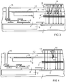
- Figure 3 is a cross section of a further CMOS-compatible chemical sensing device. Elements of the device according to Figure 3 that correspond to elements of the device according to Figure 1 are indicated with the same reference numerals.
- scattering particles 16 are arranged at the portion of the waveguide 9 that is present between the photodetector 3 and the fluorescent sensor layer 14.
- the scattering particles 16 substitute the further grating 11 used in the device according to Figure 1 .
- FIG 4 is a cross section of a further CMOS-compatible chemical sensing device. Elements of the device according to Figure 4 that correspond to elements of the device according to Figure 1 are indicated with the same reference numerals.
- a waveguide mirror 17 is arranged in the portion of the waveguide 9 that is present between the photodetector 3 and the fluorescent sensor layer 14.
- the waveguide mirror 17 is inclined with respect to the direction of propagation of the electromagnetic radiation in the waveguide 9 and reflects the guided electromagnetic radiation out of the waveguide 9.
- the waveguide mirror 17 substitutes the further grating 11 used in the device according to Figure 1 .
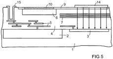
- Figure 5 is a cross section of a further CMOS-compatible chemical sensing device. Elements of the device according to Figure 5 that correspond to elements of the device according to Figure 1 are indicated with the same reference numerals.
- the waveguide 9 is not covered, and the fluorescent sensor layer 14 is directly applied on the waveguide 9.
- the evanescent light field is exploited, and no distortion within the waveguide 9 is required to couple the electromagnetic radiation out of the waveguide 9.
- the optional mirror layer 8 is of minor importance and therefore omitted in Figure 5 .
- all layers are applied on the substrate that is provided with the integrated circuit components 2 and the photodetector 3.
- the wiring 5 and the filter layer 7 are arranged in and on the dielectric 4 according to a conventional back end of line (BEOL), especially of a standard CMOS process.
- BEOL back end of line
- Cladding layers and the waveguide are formed, and the fluorescent sensor layer 14 is applied for a gas sensor or a bio sensor.
- the waveguide 9 and one metal layer provided for the mirror layer 8 are formed on a second substrate, which is then bonded to the substrate 1 comprising the integrated circuit components 2, the photodetector 3 and the wiring 5.
- the filter layer 7 can be formed on either substrate and provided with a planarization layer, especially an oxide layer.
- the described chemical sensing device allows a substantial reduction of the size of a fluorescence-based sensor and considerably increases the amount of detected fluorescence while minimizing the amount of exciting light that reaches the photodetector.
Landscapes
- Physics & Mathematics (AREA)
- Health & Medical Sciences (AREA)
- Chemical & Material Sciences (AREA)
- General Physics & Mathematics (AREA)
- Life Sciences & Earth Sciences (AREA)
- Immunology (AREA)
- Analytical Chemistry (AREA)
- Biochemistry (AREA)
- General Health & Medical Sciences (AREA)
- Pathology (AREA)
- Optics & Photonics (AREA)
- Engineering & Computer Science (AREA)
- Chemical Kinetics & Catalysis (AREA)
- Nuclear Medicine, Radiotherapy & Molecular Imaging (AREA)
- Plasma & Fusion (AREA)
- Molecular Biology (AREA)
- Microelectronics & Electronic Packaging (AREA)
- Biomedical Technology (AREA)
- Investigating, Analyzing Materials By Fluorescence Or Luminescence (AREA)
Abstract
Description
- Gas detection by some types of opto-chemical gas sensors is based on a measurement of the fluorescence of a sensing material that changes its optical properties upon exposure to specific gases. Such a gas sensor is provided with a light source, and the sensing material, which may typically be a fluorescent dye, is arranged as a thin layer, so that it can be exposed to the gas and to the light from the light source.
- The fluorescence that is displayed by the sensing material upon irradiation is detected by a photodetector. Its wavelength is usually greater than the wavelength of the exciting light emitted by the light source. There is a variety of optical properties that may be affected by a reaction between the gas and the sensing material, like spectral response, fluorescence intensity or fluorescence lifetime, for example, which allow to identify the gas and typical properties of the gas.
- A high sensitivity of the photodetector is important, because only a very small portion of the light that is incident on the sensing material is converted by fluorescence. In order to make the distance between the photodetector and the sensing material as small as possible, the light source should not be placed in between. On the other hand, an illumination of both the sensing material and the photodetector by the exciting light is to be avoided, as the photodetector is ideally only exposed to the fluorescence.
- It is an object of the present invention to provide a CMOS-compatible fluorescence-based chemical sensing device.
- This object is achieved with the chemical sensing device according to
claim 1. Embodiments derive from the dependent claims. - The chemical sensing device comprises a substrate of semiconductor material, integrated circuit components and a photodetector formed in the substrate, a dielectric on the substrate, a wiring in the dielectric, the wiring providing electric connections for the integrated circuit components and the photodetector, a source of electromagnetic radiation arranged in or above the dielectric, and a fluorescent sensor layer arranged in or above the dielectric. A waveguide is arranged in or above the dielectric. A portion of the waveguide is arranged at the source of electromagnetic radiation, so that the electromagnetic radiation emitted by the source of electromagnetic radiation is coupled into the waveguide. A further portion of the waveguide is arranged between the photodetector and the fluorescent sensor layer. The source of electromagnetic radiation may be a vertical-cavity surface-emitting laser (VCSEL) or a light-emitting diode (LED), for instance.
- An embodiment of the chemical sensing device comprises a grating in the portion of the waveguide that is arranged at the source of electromagnetic radiation, and a further grating in the portion of the waveguide that is arranged between the photodetector and the fluorescent sensor layer.
- A further embodiment comprises scattering particles at the portion of the waveguide that is arranged between the photodetector and the fluorescent sensor layer.
- A further embodiment comprises a mirror in the portion of the waveguide that is arranged between the photodetector and the fluorescent sensor layer, the mirror being inclined with respect to a direction of propagation of the electromagnetic radiation in the waveguide.
- A further embodiment comprises an optical filter arranged between the waveguide and the photodetector. The optical filter blocks the electromagnetic radiation emitted by the source of electromagnetic radiation and is transparent to radiation generated in the fluorescent sensor layer.
- A further embodiment comprises a mirror layer arranged between the waveguide and the photodetector. The mirror layer reflects the electromagnetic radiation emitted by the source of electromagnetic radiation.
- A further embodiment comprises a carrier, which is transparent to the electromagnetic radiation emitted by the source of electromagnetic radiation and to radiation generated in the fluorescent sensor layer. The fluorescent sensor layer is applied on the carrier.
- In a further embodiment the fluorescent sensor layer is directly applied on the waveguide or on a cladding layer of the waveguide.
- In a further embodiment the waveguide and the photodetector are arranged at a distance of less than 10 µm from one another.
- The fluorescent sensor layer may especially provide a gas sensor or a bio sensor.
- The following is a more detailed description of examples of the chemical sensing device in conjunction with the appended figures.
- Figure 1
- is a cross section of a chemical sensing device.
- Figure 2
- is a further cross section of the chemical sensing device according to
Figure 1 at the position indicated inFigure 1 . - Figure 3
- is a cross section of a further chemical sensing device comprising scattering particles.
- Figure 4
- is a cross section of a further chemical sensing device comprising a waveguide mirror.
- Figure 5
- is a cross section of a further chemical sensing device having a fluorescent sensor layer directly applied to a waveguide.
-
Figure 1 is a cross section of a CMOS-compatible chemical sensing device comprising a waveguide. Components of anintegrated circuit 2 and aphotodetector 3, which may be a photodiode, for instance, are formed in asubstrate 1 of semiconductor material, which may be silicon, for instance. A dielectric 4 with embedded metal layers forming awiring 5 is arranged above thesubstrate 1. Thewiring 5 provides electric connections for theintegrated circuit components 2 and thephotodetector 3. The components of anintegrated circuit 2, thephotodetector 3, the dielectric 4, and thewiring 5 may be formed in a conventional CMOS process, for instance.Figure 1 also shows acontact connection 15 for external electric connection, by way of example. - A source of
electromagnetic radiation 6, which may be a vertical-cavity surface-emitting laser (VCSEL) or a light-emitting diode (LED), for instance, is arranged in or above the dielectric 4. The source ofelectromagnetic radiation 6 may be monolithically integrated, as shown inFigure 1 , or it may be provided by an external device. Awaveguide 9 is arranged at the source ofelectromagnetic radiation 6, so that the electromagnetic radiation emitted by the source ofelectromagnetic radiation 6 can enter thewaveguide 9. The electromagnetic radiation may be coupled into thewaveguide 9 by means of a diffraction grating 10, for instance. Butt coupling may be employed instead of thegrating 10. - The
waveguide 9 may be provided with cladding layers, which may also function as optical confinement of the guided electromagnetic radiation. Cladding or confinement layers of waveguides are known per se and are not represented in the figures. Acover layer 12, which is transparent to the electromagnetic radiation from thesource 6 and to the light generated by fluorescence of the sensing material, may be applied to cover thewaveguide 9. - The electromagnetic radiation emitted by the
source 6 is guided through thewaveguide 9 to a region that is provided for sensing. Afluorescent sensing layer 14 is arranged above thephotodetector 3. The material of thefluorescent sensing layer 14 may be selected for a gas sensor or a bio sensor. In the embodiment according toFigure 1 , thefluorescent sensing layer 14 is applied on atransparent carrier 13, which is optional. Such acarrier 13 may be particularly favourable if an easy replacement of thefluorescent sensor layer 14 is desired after each measurement. Thefluorescent sensing layer 14 may instead be applied on thecover layer 12 or immediately on thewaveguide 9. - A portion of the
waveguide 9 extends between thephotodetector 3 and thefluorescent sensing layer 14. Afurther grating 11 can be provided in this portion of thewaveguide 9 to diffract the electromagnetic radiation out of thewaveguide 9 towards thefluorescent sensing layer 14. - The electromagnetic radiation that is released from the
waveguide 9 also propagates in the direction towards thephotodetector 3. As this is not desired, a monolithically integratedfilter layer 7 is arranged between thephotodetector 3 and thewaveguide 9. Thefilter layer 7, which may be an interference filter, for instance, is a bandpass filter configured to block the electromagnetic radiation emitted by thesource 6. Thefilter layer 7 is transparent to the electromagnetic radiation generated in thefluorescent sensor layer 14 and thus enhances the detection of the fluorescence in relation to the much stronger exciting light from thesource 6. - In order to increase the low conversion rate of the exciting light into fluorescence, a
mirror layer 8 may additionally be provided. The electromagnetic radiation that is diffracted from thewaveguide 9 towards thephotodetector 3 is thereby reflected in the opposite direction towards thefluorescent sensor layer 14. Themirror layer 8 may be a thin metal layer, for instance. - Several different directions of propagation of the electromagnetic radiation are indicated in
Figure 1 with arrows, by way of example. The electromagnetic radiation reaches thefluorescent sensor layer 14 directly from thewaveguide 9 or via reflection at themirror layer 8. Electromagnetic radiation generated in thefluorescent sensor layer 14 and detected by thephotodetector 3 is indicated inFigure 1 by longer vertical arrows. - The use of the
waveguide 9 allows to keep the distance between thephotodetector 3 and thefluorescent sensor layer 14 small. In particular, the distance between thephotodetector 3 and thewaveguide 9 may be smaller than 10 µm. The distance between thephotodetector 3 and thefilter layer 7 may be typically 6.5 µm, and the distance between thefilter layer 7 and thewaveguide 9 typically 3 µm, for example. -
Figure 2 is a cross section of the chemical sensing device at the position indicated inFigure 1 . The elements ofFigure 2 that correspond to elements shown inFigure 1 are indicated with the same reference numerals.Figure 2 shows twoseparate waveguides 9 at the position of thefurther grating 11; the number of individual waveguides in the device is arbitrary. The size of themirror layer 8, which can be provided for eachwaveguide 9 separately, can be adapted to the width of thewaveguide 9. Themirror layer 8 may only be present below thewaveguide 9 and cover only a portion of the area of thephotodetector 3, especially less than 50% of its area, for instance. In particular, the lateral extension of thewaveguide 9 may be smaller than the lateral extension of themirror layer 8, as shown inFigure 2 by way of example. Thefilter layer 7 may also be provided for each waveguide separately, or it may be formed as an entire layer completely covering the area of thephotodetector 3, as inFigure 2 . -
Figure 3 is a cross section of a further CMOS-compatible chemical sensing device. Elements of the device according toFigure 3 that correspond to elements of the device according toFigure 1 are indicated with the same reference numerals. In the device shown inFigure 3 , scatteringparticles 16 are arranged at the portion of thewaveguide 9 that is present between thephotodetector 3 and thefluorescent sensor layer 14. The scatteringparticles 16, which may be TiO2, for instance, scatter the guided electromagnetic radiation out of thewaveguide 9. The scatteringparticles 16 substitute thefurther grating 11 used in the device according toFigure 1 . -
Figure 4 is a cross section of a further CMOS-compatible chemical sensing device. Elements of the device according toFigure 4 that correspond to elements of the device according toFigure 1 are indicated with the same reference numerals. In the device shown inFigure 4 , awaveguide mirror 17 is arranged in the portion of thewaveguide 9 that is present between thephotodetector 3 and thefluorescent sensor layer 14. Thewaveguide mirror 17 is inclined with respect to the direction of propagation of the electromagnetic radiation in thewaveguide 9 and reflects the guided electromagnetic radiation out of thewaveguide 9. Thewaveguide mirror 17 substitutes thefurther grating 11 used in the device according toFigure 1 . -
Figure 5 is a cross section of a further CMOS-compatible chemical sensing device. Elements of the device according toFigure 5 that correspond to elements of the device according toFigure 1 are indicated with the same reference numerals. In the device shown inFigure 5 , thewaveguide 9 is not covered, and thefluorescent sensor layer 14 is directly applied on thewaveguide 9. In order to obtain an exposure of thefluorescent sensor layer 14 to the exciting light from thesource 6, the evanescent light field is exploited, and no distortion within thewaveguide 9 is required to couple the electromagnetic radiation out of thewaveguide 9. In this embodiment theoptional mirror layer 8 is of minor importance and therefore omitted inFigure 5 . - In a suitable production method for the chemical sensing device, all layers are applied on the substrate that is provided with the
integrated circuit components 2 and thephotodetector 3. Thewiring 5 and thefilter layer 7 are arranged in and on the dielectric 4 according to a conventional back end of line (BEOL), especially of a standard CMOS process. Cladding layers and the waveguide are formed, and thefluorescent sensor layer 14 is applied for a gas sensor or a bio sensor. - In an alternative production method, the
waveguide 9 and one metal layer provided for themirror layer 8 are formed on a second substrate, which is then bonded to thesubstrate 1 comprising theintegrated circuit components 2, thephotodetector 3 and thewiring 5. Thefilter layer 7 can be formed on either substrate and provided with a planarization layer, especially an oxide layer. - The described chemical sensing device allows a substantial reduction of the size of a fluorescence-based sensor and considerably increases the amount of detected fluorescence while minimizing the amount of exciting light that reaches the photodetector.
-
- 1
- substrate
- 2
- integrated circuit components
- 3
- photodetector
- 4
- dielectric
- 5
- wiring
- 6
- source of electromagnetic radiation
- 7
- filter layer
- 8
- mirror layer
- 9
- waveguide
- 10
- grating
- 11
- further grating
- 12
- cover layer
- 13
- carrier
- 14
- fluorescent sensor layer
- 15
- contact connection
- 16
- scattering particle
- 17
- waveguide mirror
Claims (12)
- A chemical sensing device, comprising:a substrate (1) of semiconductor material,integrated circuit components (2) and a photodetector (3) formed in the substrate (1),a dielectric (4) on the substrate (1),a wiring (5) in the dielectric (4), the wiring providing electric connections for the integrated circuit components (2) and the photodetector (3),a source of electromagnetic radiation (6) arranged in or above the dielectric (4), anda fluorescent sensor layer (14) arranged in or above the dielectric (4),characterized in thata waveguide (9) is arranged in or above the dielectric (4),a portion of the waveguide (9) is arranged at the source of electromagnetic radiation (6), the electromagnetic radiation emitted by the source of electromagnetic radiation (6) being coupled into the waveguide (9), anda further portion of the waveguide (9) is arranged between the photodetector (3) and the fluorescent sensor layer (14).
- The chemical sensing device according to claim 1, further comprising:a grating (10) in the portion of the waveguide (9) that is arranged at the source of electromagnetic radiation (6), anda further grating (11) in the portion of the waveguide (9) that is arranged between the photodetector (3) and the fluorescent sensor layer (14).
- The chemical sensing device according to claim 1, further comprising:scattering particles (16) at the portion of the waveguide (9) that is arranged between the photodetector (3) and the fluorescent sensor layer (14).
- The chemical sensing device according to claim 1, further comprising:a mirror (17) in the portion of the waveguide (9) that is arranged between the photodetector (3) and the fluorescent sensor layer (14), the mirror (17) being inclined with respect to a direction of propagation of the electromagnetic radiation in the waveguide (9).
- The chemical sensing device according to one of claims 1 to 4, further comprising:an optical filter (7) arranged between the waveguide (9) and the photodetector (3), the optical filter (7) blocking the electromagnetic radiation emitted by the source of electromagnetic radiation (6) and being transparent to radiation generated in the fluorescent sensor layer (14).
- The chemical sensing device according to one of claims 1 to 5, further comprising:a mirror layer (8) arranged between the waveguide (9) and the photodetector (3), the mirror layer (8) reflecting the electromagnetic radiation emitted by the source of electromagnetic radiation (6).
- The chemical sensing device according to one of claims 1 to 6, further comprising:a carrier (13), which is transparent to the electromagnetic radiation emitted by the source of electromagnetic radiation (6) and to radiation generated in the fluorescent sensor layer (14), the fluorescent sensor layer (14) being applied on the carrier (13).
- The chemical sensing device according to one of claims 1 to 6, wherein the fluorescent sensor layer (14) is directly applied on the waveguide (9).
- The chemical sensing device according to one of claims 1 to 8, wherein the source of electromagnetic radiation (6) is a vertical-cavity surface-emitting laser.
- The chemical sensing device according to one of claims 1 to 8, wherein the waveguide (9) and the photodetector (3) are arranged at a distance from one another that is less than 10 µm .
- The chemical sensing device according to one of claims 1 to 10, wherein the fluorescent sensor layer (14) provides a gas sensor.
- The chemical sensing device according to one of claims 1 to 10, wherein the fluorescent sensor layer (14) provides a bio sensor.
Priority Applications (4)
| Application Number | Priority Date | Filing Date | Title |
|---|---|---|---|
| EP17204932.2A EP3492909B1 (en) | 2017-12-01 | 2017-12-01 | Chemical sensing device using fluorescent sensing material |
| US16/766,179 US11474039B2 (en) | 2017-12-01 | 2018-11-28 | Chemical sensing device using fluorescent sensing material |
| PCT/EP2018/082867 WO2019106023A1 (en) | 2017-12-01 | 2018-11-28 | Chemical sensing device using fluorescent sensing material |
| CN201880072983.6A CN111727367B (en) | 2017-12-01 | 2018-11-28 | Chemical sensing devices using fluorescent sensing materials |
Applications Claiming Priority (1)
| Application Number | Priority Date | Filing Date | Title |
|---|---|---|---|
| EP17204932.2A EP3492909B1 (en) | 2017-12-01 | 2017-12-01 | Chemical sensing device using fluorescent sensing material |
Publications (2)
| Publication Number | Publication Date |
|---|---|
| EP3492909A1 true EP3492909A1 (en) | 2019-06-05 |
| EP3492909B1 EP3492909B1 (en) | 2023-11-01 |
Family
ID=60543466
Family Applications (1)
| Application Number | Title | Priority Date | Filing Date |
|---|---|---|---|
| EP17204932.2A Active EP3492909B1 (en) | 2017-12-01 | 2017-12-01 | Chemical sensing device using fluorescent sensing material |
Country Status (4)
| Country | Link |
|---|---|
| US (1) | US11474039B2 (en) |
| EP (1) | EP3492909B1 (en) |
| CN (1) | CN111727367B (en) |
| WO (1) | WO2019106023A1 (en) |
Cited By (1)
| Publication number | Priority date | Publication date | Assignee | Title |
|---|---|---|---|---|
| TWI852620B (en) * | 2022-10-18 | 2024-08-11 | 采鈺科技股份有限公司 | Optical device |
Families Citing this family (4)
| Publication number | Priority date | Publication date | Assignee | Title |
|---|---|---|---|---|
| WO2021038630A1 (en) * | 2019-08-23 | 2021-03-04 | 日本電信電話株式会社 | Wavelength checker |
| WO2021095165A1 (en) * | 2019-11-13 | 2021-05-20 | 日本電信電話株式会社 | Wavelength checker |
| JP7215595B2 (en) * | 2019-11-15 | 2023-01-31 | 日本電信電話株式会社 | wavelength checker |
| JP7039763B1 (en) * | 2021-11-15 | 2022-03-22 | 善文 安藤 | Vacuum channel type electronic elements, optical transmission circuits and laminated chips |
Citations (2)
| Publication number | Priority date | Publication date | Assignee | Title |
|---|---|---|---|---|
| US4755667A (en) * | 1986-10-10 | 1988-07-05 | Avl Ag | Sensor element for determination of concentration of substances |
| US6483096B1 (en) * | 1999-09-15 | 2002-11-19 | Csem Centre Suisse D'electronique Et De Microtechnique Sa | Integrated-optical chemical and biochemical sensor |
Family Cites Families (22)
| Publication number | Priority date | Publication date | Assignee | Title |
|---|---|---|---|---|
| US5082629A (en) * | 1989-12-29 | 1992-01-21 | The Board Of The University Of Washington | Thin-film spectroscopic sensor |
| KR19990014709A (en) | 1995-05-12 | 1999-02-25 | 한스루돌프하우스 | Sensor platform and method for parallel detection of multiple analytes using attenuated excited luminescence |
| CN2412225Y (en) * | 2000-03-15 | 2000-12-27 | 东南大学 | Optical reflecting sleeve for mixing rod plastic fiber glass coupler |
| US7314751B2 (en) * | 2000-10-30 | 2008-01-01 | The Charles Stark Draper Laboratory, Inc. | Fluorescence detection system including a photonic band gap structure |
| JP3934090B2 (en) * | 2003-07-09 | 2007-06-20 | 日本板硝子株式会社 | Optical multiplexer / demultiplexer for fluorescence analysis, optical module for fluorescence analysis, fluorescence analyzer, and fluorescence / photothermal conversion spectrometer |
| US7203387B2 (en) * | 2003-09-10 | 2007-04-10 | Agency For Science, Technology And Research | VLSI-photonic heterogeneous integration by wafer bonding |
| US7768650B2 (en) * | 2004-04-21 | 2010-08-03 | Michael Bazylenko | Optoelectronic biochip |
| US8349605B1 (en) * | 2005-04-12 | 2013-01-08 | Colorado State University Research Foundation | Optical analyte sensor |
| US7801394B2 (en) * | 2005-10-03 | 2010-09-21 | Creatv Microtech, Inc. | Sensitive emission light gathering and detection system |
| US8570518B2 (en) * | 2007-01-31 | 2013-10-29 | Alverix, Inc. | Methods and materials for detection of target species |
| US20090087137A1 (en) * | 2007-10-02 | 2009-04-02 | My The Doan | Planar lightwave circuits with air filled trenches |
| JP5001119B2 (en) | 2007-11-22 | 2012-08-15 | アズビル株式会社 | Temperature sensor probe and manufacturing method thereof |
| US20110013868A1 (en) * | 2007-12-17 | 2011-01-20 | Kouji Suzumura | Optical waveguide for visible light |
| BRPI0908090A2 (en) * | 2008-02-25 | 2015-08-25 | Koninkl Philips Electronics Nv | Optical sensor and method for measuring light radiating from an analyte upon light excitation, and part kit |
| FR2970079B1 (en) * | 2010-12-29 | 2022-08-12 | Genewave | BIOCHIP TYPE DEVICE |
| CN102507520B (en) * | 2011-11-03 | 2013-07-03 | 常州博世伟业生物科技有限公司 | Liquid core waveguide fluorescence detector |
| EP2606974A1 (en) | 2011-12-19 | 2013-06-26 | Nxp B.V. | An optical detection system, a cartridge therefor and a reader therefor |
| EP2772939B1 (en) * | 2013-03-01 | 2016-10-19 | Ams Ag | Semiconductor device for detection of radiation and method of producing a semiconductor device for detection of radiation |
| EP2881773B1 (en) * | 2013-12-03 | 2018-07-11 | ams AG | Semiconductor device with integrated mirror and method of producing a semiconductor device with integrated mirror |
| US9816935B2 (en) * | 2014-01-23 | 2017-11-14 | Imec Vzw | Integrated waveguide structure for fluorescence analysis |
| US9632251B2 (en) * | 2014-04-02 | 2017-04-25 | International Business Machines Corporation | Integration of photonic, electronic, and sensor devices with SOI VLSI microprocessor technology |
| JP2014194435A (en) * | 2014-07-01 | 2014-10-09 | Toshiba Corp | Optical waveguide type biochemical sensor chip |
-
2017
- 2017-12-01 EP EP17204932.2A patent/EP3492909B1/en active Active
-
2018
- 2018-11-28 WO PCT/EP2018/082867 patent/WO2019106023A1/en not_active Ceased
- 2018-11-28 CN CN201880072983.6A patent/CN111727367B/en active Active
- 2018-11-28 US US16/766,179 patent/US11474039B2/en active Active
Patent Citations (2)
| Publication number | Priority date | Publication date | Assignee | Title |
|---|---|---|---|---|
| US4755667A (en) * | 1986-10-10 | 1988-07-05 | Avl Ag | Sensor element for determination of concentration of substances |
| US6483096B1 (en) * | 1999-09-15 | 2002-11-19 | Csem Centre Suisse D'electronique Et De Microtechnique Sa | Integrated-optical chemical and biochemical sensor |
Cited By (1)
| Publication number | Priority date | Publication date | Assignee | Title |
|---|---|---|---|---|
| TWI852620B (en) * | 2022-10-18 | 2024-08-11 | 采鈺科技股份有限公司 | Optical device |
Also Published As
| Publication number | Publication date |
|---|---|
| US11474039B2 (en) | 2022-10-18 |
| WO2019106023A1 (en) | 2019-06-06 |
| EP3492909B1 (en) | 2023-11-01 |
| CN111727367A (en) | 2020-09-29 |
| CN111727367B (en) | 2023-04-28 |
| US20200284727A1 (en) | 2020-09-10 |
Similar Documents
| Publication | Publication Date | Title |
|---|---|---|
| US11474039B2 (en) | Chemical sensing device using fluorescent sensing material | |
| US7095502B2 (en) | Optical structures for metal-enhanced sensing | |
| US8263945B2 (en) | Optical wavelength demultiplexing detector for fluorescence analysis and fluorescence detection system | |
| JP2007171186A (en) | Sample detection system | |
| JPS6398548A (en) | Sensor element for measuring substance concentration | |
| JP6360430B2 (en) | Sensor apparatus and method based on wavelength center detection | |
| US20120012739A1 (en) | Optical microresonator system | |
| US20210063318A1 (en) | Detection device for detecting contamination | |
| CN109073169A (en) | Light source based on laser | |
| US6211954B1 (en) | Integrated optical luminescence sensor | |
| WO2006081566A1 (en) | Integrated system and method for transversal enhanced raman spectroscopy | |
| WO2006081567A1 (en) | Integrated modular system and method for enhanced raman spectroscopy | |
| JP2018518669A (en) | Optical analysis system with optical delivery of an optical conduit | |
| US12460967B2 (en) | Integrated bound-mode spectral/angular sensors | |
| US8253933B2 (en) | Waveguide-based sensor | |
| JPWO2017060992A1 (en) | Endoscope lighting system | |
| CN116660149A (en) | sensor | |
| JP2006125860A (en) | Surface plasmon sensor and surface plasmon measuring device | |
| US11442234B2 (en) | Device and method for transferring light between at least one optoelectronic component and at least one optical waveguide | |
| EP4545920A1 (en) | Miniature nir spectrometer with wedged module window | |
| JP2007101241A (en) | Sensing device | |
| EP4603807A1 (en) | Phase change material as switchable optical element | |
| WO2026082650A1 (en) | Tir-free spectrometry with transmission gratings | |
| JP2010096716A (en) | Infrared camera | |
| Sumpf et al. | 5,000 h reliable operation of 785nm dual-wavelength DBR-RW diode lasers suitable for Raman spectroscopy and SERDS |
Legal Events
| Date | Code | Title | Description |
|---|---|---|---|
| PUAI | Public reference made under article 153(3) epc to a published international application that has entered the european phase |
Free format text: ORIGINAL CODE: 0009012 |
|
| STAA | Information on the status of an ep patent application or granted ep patent |
Free format text: STATUS: THE APPLICATION HAS BEEN PUBLISHED |
|
| AK | Designated contracting states |
Kind code of ref document: A1 Designated state(s): AL AT BE BG CH CY CZ DE DK EE ES FI FR GB GR HR HU IE IS IT LI LT LU LV MC MK MT NL NO PL PT RO RS SE SI SK SM TR |
|
| AX | Request for extension of the european patent |
Extension state: BA ME |
|
| STAA | Information on the status of an ep patent application or granted ep patent |
Free format text: STATUS: REQUEST FOR EXAMINATION WAS MADE |
|
| 17P | Request for examination filed |
Effective date: 20191009 |
|
| RBV | Designated contracting states (corrected) |
Designated state(s): AL AT BE BG CH CY CZ DE DK EE ES FI FR GB GR HR HU IE IS IT LI LT LU LV MC MK MT NL NO PL PT RO RS SE SI SK SM TR |
|
| STAA | Information on the status of an ep patent application or granted ep patent |
Free format text: STATUS: EXAMINATION IS IN PROGRESS |
|
| 17Q | First examination report despatched |
Effective date: 20220303 |
|
| REG | Reference to a national code |
Ref legal event code: R079 Free format text: PREVIOUS MAIN CLASS: G01N0021770000 Ref country code: DE Ref legal event code: R079 Ref document number: 602017075937 Country of ref document: DE Free format text: PREVIOUS MAIN CLASS: G01N0021770000 Ipc: G02B0006120000 |
|
| GRAP | Despatch of communication of intention to grant a patent |
Free format text: ORIGINAL CODE: EPIDOSNIGR1 |
|
| STAA | Information on the status of an ep patent application or granted ep patent |
Free format text: STATUS: GRANT OF PATENT IS INTENDED |
|
| RIC1 | Information provided on ipc code assigned before grant |
Ipc: G01N 21/77 20060101ALI20230703BHEP Ipc: G02B 6/12 20060101AFI20230703BHEP |
|
| INTG | Intention to grant announced |
Effective date: 20230725 |
|
| P01 | Opt-out of the competence of the unified patent court (upc) registered |
Effective date: 20230724 |
|
| GRAS | Grant fee paid |
Free format text: ORIGINAL CODE: EPIDOSNIGR3 |
|
| GRAA | (expected) grant |
Free format text: ORIGINAL CODE: 0009210 |
|
| STAA | Information on the status of an ep patent application or granted ep patent |
Free format text: STATUS: THE PATENT HAS BEEN GRANTED |
|
| AK | Designated contracting states |
Kind code of ref document: B1 Designated state(s): AL AT BE BG CH CY CZ DE DK EE ES FI FR GB GR HR HU IE IS IT LI LT LU LV MC MK MT NL NO PL PT RO RS SE SI SK SM TR |
|
| REG | Reference to a national code |
Ref country code: GB Ref legal event code: FG4D |
|
| REG | Reference to a national code |
Ref country code: CH Ref legal event code: EP |
|
| REG | Reference to a national code |
Ref country code: IE Ref legal event code: FG4D |
|
| REG | Reference to a national code |
Ref country code: DE Ref legal event code: R096 Ref document number: 602017075937 Country of ref document: DE |
|
| REG | Reference to a national code |
Ref country code: LT Ref legal event code: MG9D |
|
| REG | Reference to a national code |
Ref country code: NL Ref legal event code: MP Effective date: 20231101 |
|
| PG25 | Lapsed in a contracting state [announced via postgrant information from national office to epo] |
Ref country code: GR Free format text: LAPSE BECAUSE OF FAILURE TO SUBMIT A TRANSLATION OF THE DESCRIPTION OR TO PAY THE FEE WITHIN THE PRESCRIBED TIME-LIMIT Effective date: 20240202 |
|
| PG25 | Lapsed in a contracting state [announced via postgrant information from national office to epo] |
Ref country code: IS Free format text: LAPSE BECAUSE OF FAILURE TO SUBMIT A TRANSLATION OF THE DESCRIPTION OR TO PAY THE FEE WITHIN THE PRESCRIBED TIME-LIMIT Effective date: 20240301 |
|
| PG25 | Lapsed in a contracting state [announced via postgrant information from national office to epo] |
Ref country code: LT Free format text: LAPSE BECAUSE OF FAILURE TO SUBMIT A TRANSLATION OF THE DESCRIPTION OR TO PAY THE FEE WITHIN THE PRESCRIBED TIME-LIMIT Effective date: 20231101 |
|
| REG | Reference to a national code |
Ref country code: AT Ref legal event code: MK05 Ref document number: 1627860 Country of ref document: AT Kind code of ref document: T Effective date: 20231101 |
|
| PG25 | Lapsed in a contracting state [announced via postgrant information from national office to epo] |
Ref country code: NL Free format text: LAPSE BECAUSE OF FAILURE TO SUBMIT A TRANSLATION OF THE DESCRIPTION OR TO PAY THE FEE WITHIN THE PRESCRIBED TIME-LIMIT Effective date: 20231101 |
|
| PG25 | Lapsed in a contracting state [announced via postgrant information from national office to epo] |
Ref country code: AT Free format text: LAPSE BECAUSE OF FAILURE TO SUBMIT A TRANSLATION OF THE DESCRIPTION OR TO PAY THE FEE WITHIN THE PRESCRIBED TIME-LIMIT Effective date: 20231101 |
|
| PG25 | Lapsed in a contracting state [announced via postgrant information from national office to epo] |
Ref country code: ES Free format text: LAPSE BECAUSE OF FAILURE TO SUBMIT A TRANSLATION OF THE DESCRIPTION OR TO PAY THE FEE WITHIN THE PRESCRIBED TIME-LIMIT Effective date: 20231101 |
|
| PG25 | Lapsed in a contracting state [announced via postgrant information from national office to epo] |
Ref country code: NL Free format text: LAPSE BECAUSE OF FAILURE TO SUBMIT A TRANSLATION OF THE DESCRIPTION OR TO PAY THE FEE WITHIN THE PRESCRIBED TIME-LIMIT Effective date: 20231101 Ref country code: LT Free format text: LAPSE BECAUSE OF FAILURE TO SUBMIT A TRANSLATION OF THE DESCRIPTION OR TO PAY THE FEE WITHIN THE PRESCRIBED TIME-LIMIT Effective date: 20231101 Ref country code: IS Free format text: LAPSE BECAUSE OF FAILURE TO SUBMIT A TRANSLATION OF THE DESCRIPTION OR TO PAY THE FEE WITHIN THE PRESCRIBED TIME-LIMIT Effective date: 20240301 Ref country code: GR Free format text: LAPSE BECAUSE OF FAILURE TO SUBMIT A TRANSLATION OF THE DESCRIPTION OR TO PAY THE FEE WITHIN THE PRESCRIBED TIME-LIMIT Effective date: 20240202 Ref country code: ES Free format text: LAPSE BECAUSE OF FAILURE TO SUBMIT A TRANSLATION OF THE DESCRIPTION OR TO PAY THE FEE WITHIN THE PRESCRIBED TIME-LIMIT Effective date: 20231101 Ref country code: BG Free format text: LAPSE BECAUSE OF FAILURE TO SUBMIT A TRANSLATION OF THE DESCRIPTION OR TO PAY THE FEE WITHIN THE PRESCRIBED TIME-LIMIT Effective date: 20240201 Ref country code: AT Free format text: LAPSE BECAUSE OF FAILURE TO SUBMIT A TRANSLATION OF THE DESCRIPTION OR TO PAY THE FEE WITHIN THE PRESCRIBED TIME-LIMIT Effective date: 20231101 Ref country code: PT Free format text: LAPSE BECAUSE OF FAILURE TO SUBMIT A TRANSLATION OF THE DESCRIPTION OR TO PAY THE FEE WITHIN THE PRESCRIBED TIME-LIMIT Effective date: 20240301 |
|
| PG25 | Lapsed in a contracting state [announced via postgrant information from national office to epo] |
Ref country code: SE Free format text: LAPSE BECAUSE OF FAILURE TO SUBMIT A TRANSLATION OF THE DESCRIPTION OR TO PAY THE FEE WITHIN THE PRESCRIBED TIME-LIMIT Effective date: 20231101 Ref country code: RS Free format text: LAPSE BECAUSE OF FAILURE TO SUBMIT A TRANSLATION OF THE DESCRIPTION OR TO PAY THE FEE WITHIN THE PRESCRIBED TIME-LIMIT Effective date: 20231101 Ref country code: PL Free format text: LAPSE BECAUSE OF FAILURE TO SUBMIT A TRANSLATION OF THE DESCRIPTION OR TO PAY THE FEE WITHIN THE PRESCRIBED TIME-LIMIT Effective date: 20231101 Ref country code: NO Free format text: LAPSE BECAUSE OF FAILURE TO SUBMIT A TRANSLATION OF THE DESCRIPTION OR TO PAY THE FEE WITHIN THE PRESCRIBED TIME-LIMIT Effective date: 20240201 Ref country code: LV Free format text: LAPSE BECAUSE OF FAILURE TO SUBMIT A TRANSLATION OF THE DESCRIPTION OR TO PAY THE FEE WITHIN THE PRESCRIBED TIME-LIMIT Effective date: 20231101 Ref country code: HR Free format text: LAPSE BECAUSE OF FAILURE TO SUBMIT A TRANSLATION OF THE DESCRIPTION OR TO PAY THE FEE WITHIN THE PRESCRIBED TIME-LIMIT Effective date: 20231101 |
|
| PG25 | Lapsed in a contracting state [announced via postgrant information from national office to epo] |
Ref country code: DK Free format text: LAPSE BECAUSE OF FAILURE TO SUBMIT A TRANSLATION OF THE DESCRIPTION OR TO PAY THE FEE WITHIN THE PRESCRIBED TIME-LIMIT Effective date: 20231101 |
|
| PG25 | Lapsed in a contracting state [announced via postgrant information from national office to epo] |
Ref country code: CZ Free format text: LAPSE BECAUSE OF FAILURE TO SUBMIT A TRANSLATION OF THE DESCRIPTION OR TO PAY THE FEE WITHIN THE PRESCRIBED TIME-LIMIT Effective date: 20231101 |
|
| PG25 | Lapsed in a contracting state [announced via postgrant information from national office to epo] |
Ref country code: SK Free format text: LAPSE BECAUSE OF FAILURE TO SUBMIT A TRANSLATION OF THE DESCRIPTION OR TO PAY THE FEE WITHIN THE PRESCRIBED TIME-LIMIT Effective date: 20231101 |
|
| PG25 | Lapsed in a contracting state [announced via postgrant information from national office to epo] |
Ref country code: SM Free format text: LAPSE BECAUSE OF FAILURE TO SUBMIT A TRANSLATION OF THE DESCRIPTION OR TO PAY THE FEE WITHIN THE PRESCRIBED TIME-LIMIT Effective date: 20231101 Ref country code: SK Free format text: LAPSE BECAUSE OF FAILURE TO SUBMIT A TRANSLATION OF THE DESCRIPTION OR TO PAY THE FEE WITHIN THE PRESCRIBED TIME-LIMIT Effective date: 20231101 Ref country code: RO Free format text: LAPSE BECAUSE OF FAILURE TO SUBMIT A TRANSLATION OF THE DESCRIPTION OR TO PAY THE FEE WITHIN THE PRESCRIBED TIME-LIMIT Effective date: 20231101 Ref country code: IT Free format text: LAPSE BECAUSE OF FAILURE TO SUBMIT A TRANSLATION OF THE DESCRIPTION OR TO PAY THE FEE WITHIN THE PRESCRIBED TIME-LIMIT Effective date: 20231101 Ref country code: EE Free format text: LAPSE BECAUSE OF FAILURE TO SUBMIT A TRANSLATION OF THE DESCRIPTION OR TO PAY THE FEE WITHIN THE PRESCRIBED TIME-LIMIT Effective date: 20231101 Ref country code: DK Free format text: LAPSE BECAUSE OF FAILURE TO SUBMIT A TRANSLATION OF THE DESCRIPTION OR TO PAY THE FEE WITHIN THE PRESCRIBED TIME-LIMIT Effective date: 20231101 Ref country code: CZ Free format text: LAPSE BECAUSE OF FAILURE TO SUBMIT A TRANSLATION OF THE DESCRIPTION OR TO PAY THE FEE WITHIN THE PRESCRIBED TIME-LIMIT Effective date: 20231101 |
|
| REG | Reference to a national code |
Ref country code: CH Ref legal event code: PL |
|
| REG | Reference to a national code |
Ref country code: DE Ref legal event code: R097 Ref document number: 602017075937 Country of ref document: DE |
|
| PG25 | Lapsed in a contracting state [announced via postgrant information from national office to epo] |
Ref country code: LU Free format text: LAPSE BECAUSE OF NON-PAYMENT OF DUE FEES Effective date: 20231201 |
|
| PG25 | Lapsed in a contracting state [announced via postgrant information from national office to epo] |
Ref country code: MC Free format text: LAPSE BECAUSE OF FAILURE TO SUBMIT A TRANSLATION OF THE DESCRIPTION OR TO PAY THE FEE WITHIN THE PRESCRIBED TIME-LIMIT Effective date: 20231101 |
|
| REG | Reference to a national code |
Ref country code: BE Ref legal event code: MM Effective date: 20231231 |
|
| PG25 | Lapsed in a contracting state [announced via postgrant information from national office to epo] |
Ref country code: MC Free format text: LAPSE BECAUSE OF FAILURE TO SUBMIT A TRANSLATION OF THE DESCRIPTION OR TO PAY THE FEE WITHIN THE PRESCRIBED TIME-LIMIT Effective date: 20231101 Ref country code: LU Free format text: LAPSE BECAUSE OF NON-PAYMENT OF DUE FEES Effective date: 20231201 |
|
| PLBE | No opposition filed within time limit |
Free format text: ORIGINAL CODE: 0009261 |
|
| STAA | Information on the status of an ep patent application or granted ep patent |
Free format text: STATUS: NO OPPOSITION FILED WITHIN TIME LIMIT |
|
| 26N | No opposition filed |
Effective date: 20240802 |
|
| REG | Reference to a national code |
Ref country code: IE Ref legal event code: MM4A |
|
| PG25 | Lapsed in a contracting state [announced via postgrant information from national office to epo] |
Ref country code: IE Free format text: LAPSE BECAUSE OF NON-PAYMENT OF DUE FEES Effective date: 20231201 |
|
| PG25 | Lapsed in a contracting state [announced via postgrant information from national office to epo] |
Ref country code: BE Free format text: LAPSE BECAUSE OF NON-PAYMENT OF DUE FEES Effective date: 20231231 |
|
| PG25 | Lapsed in a contracting state [announced via postgrant information from national office to epo] |
Ref country code: FR Free format text: LAPSE BECAUSE OF NON-PAYMENT OF DUE FEES Effective date: 20240101 |
|
| PG25 | Lapsed in a contracting state [announced via postgrant information from national office to epo] |
Ref country code: CH Free format text: LAPSE BECAUSE OF NON-PAYMENT OF DUE FEES Effective date: 20231231 |
|
| GBPC | Gb: european patent ceased through non-payment of renewal fee |
Effective date: 20240201 |
|
| PG25 | Lapsed in a contracting state [announced via postgrant information from national office to epo] |
Ref country code: SI Free format text: LAPSE BECAUSE OF FAILURE TO SUBMIT A TRANSLATION OF THE DESCRIPTION OR TO PAY THE FEE WITHIN THE PRESCRIBED TIME-LIMIT Effective date: 20231101 |
|
| PG25 | Lapsed in a contracting state [announced via postgrant information from national office to epo] |
Ref country code: SI Free format text: LAPSE BECAUSE OF FAILURE TO SUBMIT A TRANSLATION OF THE DESCRIPTION OR TO PAY THE FEE WITHIN THE PRESCRIBED TIME-LIMIT Effective date: 20231101 Ref country code: IE Free format text: LAPSE BECAUSE OF NON-PAYMENT OF DUE FEES Effective date: 20231201 Ref country code: FR Free format text: LAPSE BECAUSE OF NON-PAYMENT OF DUE FEES Effective date: 20240101 Ref country code: CH Free format text: LAPSE BECAUSE OF NON-PAYMENT OF DUE FEES Effective date: 20231231 Ref country code: BE Free format text: LAPSE BECAUSE OF NON-PAYMENT OF DUE FEES Effective date: 20231231 |
|
| PG25 | Lapsed in a contracting state [announced via postgrant information from national office to epo] |
Ref country code: GB Free format text: LAPSE BECAUSE OF NON-PAYMENT OF DUE FEES Effective date: 20240201 |
|
| PG25 | Lapsed in a contracting state [announced via postgrant information from national office to epo] |
Ref country code: GB Free format text: LAPSE BECAUSE OF NON-PAYMENT OF DUE FEES Effective date: 20240201 |
|
| PG25 | Lapsed in a contracting state [announced via postgrant information from national office to epo] |
Ref country code: FI Free format text: LAPSE BECAUSE OF FAILURE TO SUBMIT A TRANSLATION OF THE DESCRIPTION OR TO PAY THE FEE WITHIN THE PRESCRIBED TIME-LIMIT Effective date: 20231101 |
|
| PG25 | Lapsed in a contracting state [announced via postgrant information from national office to epo] |
Ref country code: CY Free format text: LAPSE BECAUSE OF FAILURE TO SUBMIT A TRANSLATION OF THE DESCRIPTION OR TO PAY THE FEE WITHIN THE PRESCRIBED TIME-LIMIT; INVALID AB INITIO Effective date: 20171201 |
|
| PG25 | Lapsed in a contracting state [announced via postgrant information from national office to epo] |
Ref country code: HU Free format text: LAPSE BECAUSE OF FAILURE TO SUBMIT A TRANSLATION OF THE DESCRIPTION OR TO PAY THE FEE WITHIN THE PRESCRIBED TIME-LIMIT; INVALID AB INITIO Effective date: 20171201 |
|
| PG25 | Lapsed in a contracting state [announced via postgrant information from national office to epo] |
Ref country code: TR Free format text: LAPSE BECAUSE OF FAILURE TO SUBMIT A TRANSLATION OF THE DESCRIPTION OR TO PAY THE FEE WITHIN THE PRESCRIBED TIME-LIMIT Effective date: 20231101 |
|
| PGFP | Annual fee paid to national office [announced via postgrant information from national office to epo] |
Ref country code: DE Payment date: 20251211 Year of fee payment: 9 |