EP3490168A1 - Single photodiode optical full field detector - Google Patents
Single photodiode optical full field detector Download PDFInfo
- Publication number
- EP3490168A1 EP3490168A1 EP17306631.7A EP17306631A EP3490168A1 EP 3490168 A1 EP3490168 A1 EP 3490168A1 EP 17306631 A EP17306631 A EP 17306631A EP 3490168 A1 EP3490168 A1 EP 3490168A1
- Authority
- EP
- European Patent Office
- Prior art keywords
- signal
- along
- polarization
- optical signal
- incoming optical
- Prior art date
- Legal status (The legal status is an assumption and is not a legal conclusion. Google has not performed a legal analysis and makes no representation as to the accuracy of the status listed.)
- Granted
Links
Images




Classifications
-
- H—ELECTRICITY
- H04—ELECTRIC COMMUNICATION TECHNIQUE
- H04B—TRANSMISSION
- H04B10/00—Transmission systems employing electromagnetic waves other than radio-waves, e.g. infrared, visible or ultraviolet light, or employing corpuscular radiation, e.g. quantum communication
- H04B10/60—Receivers
- H04B10/61—Coherent receivers
- H04B10/616—Details of the electronic signal processing in coherent optical receivers
- H04B10/6166—Polarisation demultiplexing, tracking or alignment of orthogonal polarisation components
-
- H—ELECTRICITY
- H04—ELECTRIC COMMUNICATION TECHNIQUE
- H04B—TRANSMISSION
- H04B10/00—Transmission systems employing electromagnetic waves other than radio-waves, e.g. infrared, visible or ultraviolet light, or employing corpuscular radiation, e.g. quantum communication
- H04B10/50—Transmitters
- H04B10/516—Details of coding or modulation
- H04B10/532—Polarisation modulation
-
- H—ELECTRICITY
- H04—ELECTRIC COMMUNICATION TECHNIQUE
- H04J—MULTIPLEX COMMUNICATION
- H04J14/00—Optical multiplex systems
- H04J14/06—Polarisation multiplex systems
Definitions
- the present invention relates to an optical full field detector adapted to simultaneously detect the phase and amplitude of the polarization states of an incoming optical signal.
- optical field detection is actively leveraged in our daily lives.
- the properties of the full optical field i.e. herein defined as an electromagnetic field
- Each of the discussed dimensions potentially conveys independent information, thus offering uncoupled perspectives of the same content that will always improve/accelerate its interpretation/demodulation as compared to single-dimension systems (e.g. detecting the intensity of the field only); exactly like color and shape cooperate to better identify an object when we observe it.
- single-dimension systems e.g. detecting the intensity of the field only
- exactly like color and shape cooperate to better identify an object when we observe it.
- low-cost full optical-field detection is desirable in a large range of the applications.
- the frequency range of the optical signals transmitted and data processed is usually the infra-red frequency range.
- the employed detection techniques as of today elude a suitable trade-off between the number of dimensions that they can track and their cost and hardware complexity.
- Figure 1 represents a direct detection device DDD consisting of a photodiode PD.
- the photodiode PD receives an optical signal and converts the photons of the optical signal 1 into an electrical current 2 that is proportional to the intensity of the optical signal's field 1.
- optical intensity detection Such process is called optical intensity detection.
- Figure 2 represents a polarization-diversity coherent detector PDCD.
- This detector PDCD consists of a local oscillator LO, two polarization splitters PS1 and PS2, two 90° optical hybrid 90_X and 90_Y, four balanced photodiodes BPD1 to BPD4, and a 4x4 analog-to-digital converter ADC (four inputs and four outputs).
- the purpose is to project the four characteristic dimensions of the optical signal 1 to analyse into several photodiodes BPD1 to BPD4, each capturing the properties of the field in various complementary intensity vectors.
- the polarization states X and Y constituting the optical signal 1 are split by one of the polarization splitter PS1.
- the same thing is done with the polarization states X and Y of the local oscillator LO, that is a well-known and controlled signal, by the other polarized splitter PS2.
- the signals polarized according to X are sent into one of the 90° optical hybrid 90_X and the signals polarized according to Y are sent into one of the 90° optical hybrid 90_Y.
- Each 90° optical hybrid 90_X and 90_Y will split the signal coming from the local oscillator in two identical sub-signals as well as for the signal coming from the optical signal to analyse. Then the 90° optical hybrid 90_X and 90_Y will combine one of the sub-signal coming from the local oscillator with one of the sub-signal coming from the optical signal and it will phase shift by 90° the other sub-signal coming from the local oscillator before combining it to the other sub-signal coming from the optical signal.
- the four digital signals obtained I_X, Q_X, I_Y and Q_Y respectively correspond to the in-phase of the optical signal 1 in polarization X, the quadrature of the optical signal 1 in polarization X, the in-phase of the optical signal 1 in polarization Y, and the quadrature of the optical signal 1 in polarization Y.
- these four digital signals obtained enable to recover the amplitude and phase of both polarization states of the optical signal 1 which correspond to the full detection or the four parameters or dimensions of the optical signal 1.
- the dimensional diversity is maximum, but we are adding a substantial amount of pieces of hardware and post-detection digital signal processing that surely increases the cost, the power consumption, and the form factor; making this receiver structure prohibitive in, for instance, low-profile sensing applications or cost-critical short-reach Datacom systems
- the present invention proposes an optical full field detector for an incoming optical signal to solve the prior art drawbacks.
- n an integer comprised between [0; 2].
- the optical full field detector is adapted to simultaneously detect the phase and amplitude of the polarization states of the incoming optical signal, and comprises:
- the optical full field detector further comprises the following technical features taken alone or in combination:
- the digital signal processor further comprises:
- the present invention also proposes an encoding method for encoding an incoming optical signal.
- n an integer comprised between [0; 2]
- the encoding method comprising:
- the encoding method further comprises the following technical features taken alone or in combination:
- the present invention further proposes a decoding method for and incoming optical signal encoded according to the encoding method previously cited.
- the decoding method comprises:
- an optical full field detector 100 for an incoming signal S is adapted to simultaneously detect the phase and amplitude of the polarization states of the incoming optical signal S.
- the incoming optical signal S to be detected has a central frequency f 0 and a bandwidth B and may comprise n polarization states, n being an integer comprised between [0; 2].
- s H bb (t) and s V bb (t) are the complex baseband signals in both polarizations (these complex signals are made by the in-phase and quadrature components, therefore there are four independent dimensions considering the two polarizations).
- the frequency response of the incoming optical signal S has one of its amplitude
- are different from zero.
- B is typically a few GHz for optical communications applications.
- the optical full field detector 100 comprises:
- the first polarization maintaining coupler PMC1 is adapted to couple the polarized signal along the first direction H of the incoming optical signal S with the first laser LH (also called "tone 1") and maintain the polarization along the first direction H of this first obtained signal.
- the second polarization maintaining coupler PMC2 is adapted to couple the polarized signal along the second direction V of the incoming optical signal S with the second laser LV (also called "tone 2") and maintain the polarization along the second direction V of this second obtained signal.
- the polarization beam combiner is adapted to combine (or multiplex) the first and second obtained signals into a coupled optical signal.
- a 1 and A 2 are respectively the amplitude of the tone 1 and of the tone 2.
- Figure 5 illustrates the frequency response of coupled optical signal, at the measurement point B' in Figure 3 , which corresponds to the incoming optical signal S of Figure 4 after the addition of the two tones with frequencies f 1 and f 2 .
- the opto-electronic converter OEC is adapted to receive and convert the coupled optical signal into an electrical signal ES.
- the opto-electronic converter OEC can be a photodiode.
- the output I(t) of the opto-electronic converter OEC corresponding to the electrical signal ES can be written as follow: I t ⁇ y H t 2 + y v t 2 which after some development becomes I t ⁇ DC + Re s H bb t * exp j 2 ⁇ f 0 ⁇ t 1 t + Re s V bb t * exp j 2 ⁇ f 0 ⁇ f 2 t + NL where:
- the analog-to-digital converter ADC is adapted to receive and convert the electrical signal ES into a digital signal DS.
- the analog-to-digital converter ADC samples the electrical signal ES obtained at the output of opto-electronic at a frequency f s per second before converting it into a digital signal DS.
- the frequency f s is in the order of tens of giga samples per second for communications applications.
- the digital signal processor DSP is adapted to receive the digital signal DS and to extract from the digital signal DS the phase and amplitude of the n polarization states of the incoming optical signal S.
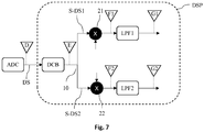
- Figure 7 illustrates a digital signal processor DSP according to an embodiment that can be used in the first and general embodiment of the optical full field detector.
- DSP digital signal processor
- the digital signal processor DSP comprises:
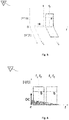
- Figures 8a to 8c show the amplitude of the frequency response in each step of the process performed in the digital signal processor DSP.
- Figure 8a illustrates the amplitude of the frequency response of the digital signal DS at the measurement point D in Figures 3 and 7 which corresponds to the input of the digital signal processor DSP. Both positive and negative frequencies are represented here. The diagram is similar to the one of Figure 6 . For real signals the spectral content in the negative frequencies of the frequency response has the same content as the positive frequencies thus the amplitude of the frequency response is symmetric.
- a first block centered around frequency (f 1 - fo) Hz and its symmetrical block centered around frequency - (f 1 - fo) Hz, both having a bandwidth of B, correspond to the combination of the part of the incoming signal S polarized along the first direction H and the first laser LH.
- Figure 8b illustrates the amplitude of the frequency response of the digital signal DS at the measurement point E in Figure 7 which corresponds to the output of the first filter DCB, so after the filtering of the constant value DC of the digital signal DS.
- the first shifting element 21 is adapted to shift in frequency one of the sub-digital signal S-DS1 so that the first low pass filter LPF1 is adapted to filter the part of the sub-digital signal which contains the information of the phase and amplitude of the polarization state along the first direction H of the incoming optical signal S.
- Figure 8c illustrates the amplitude of the frequency response of this sub-digital signal S-DS1 at the measurement point F1 in Figure 7 , so after its shifting in frequency at the output of the first shifting element 21 also corresponding to the input of the first low pass filter LPF1.
- Figure 8d illustrates the amplitude of the frequency response of the sub-digital signal S-DS1 at the measurement point G1 in Figure 7 , which corresponds to the output of the first low pass filter LPF1, so after its shifting in frequency by the first shifting element 21 and its filtering by the first low pass filter LPF1.
- This signal is complex-valued and contains in-phase and quadrature components of polarization state of the incoming optical signal S along the first direction H.
- the second shifting element 22 is adapted to shift in frequency the other sub-digital signal S-DS2 so that the second low pass filter LPF2 is adapted to filter the part of the sub-digital signal S-DS2 which contains the information of the phase and amplitude of the polarization state along the second direction V of the incoming optical signal S.
- Figure 9a illustrates the amplitude of the frequency response of this sub-digital signal S-DS2 at the measurement point F2 in Figure 7 , so after its shifting in frequency at the output of the second shifting element 22 also corresponding to the input of the second low pass filter LPF2.
- Figure 9b illustrates the amplitude of the frequency response of the sub-digital signal S-DS2 at the measurement point G2 in Figure 7 which corresponds to the output of the second low pass filter LPF2, so after its shifting in frequency by the second shifting element 22 and its filtering by the second low pass filter LPF2.
- This signal is complex-valued and contains in-phase and quadrature components of polarization state of the incoming optical signal S along the second direction V.
- the shift in frequency is realized by multiplying the first sub-digital signal S-DS1 by an exponential with frequency (f 1 -f 0 ) for the polarisation along the first direction H, and by multiplying the second sub-digital signal S-DS2 by an exponential with frequency (f 2 -f 0 ).
- the first and second low pass filter used are typically 3 dB bandwidth of around B/2 Hz to filter the undesired neighbouring signals. These filters have also to consider the uncertainty of the lasers frequencies to not filter the edges of the desired signal.
- the cut-off frequency f c is equal to B/2 Hz with a precision of - 0 Hz / + 3 GHz. In fact, if the cut-off frequency f c is under B/2 Hz there will be a loss of information, and the uncertainty of laser are normally 1.5 GHz in telecom applications.
- both signals obtained at the output G1 and G2 of the first and second low pass filter LPF1 and LPF2 are corrupted by some nonlinearity, but as we have mentioned this can very low depending on the ratio between tone and signal power. This can also be completely or partially compensated in signal processing using nonlinear equalizers. Finally, we could potentially recover the unknown frequency as well as the random phase fluctuations coming from difference of nominal and actual frequency and phase noise. Usually this is done by a phase locked loop (PLL).
- PLL phase locked loop
- each shifting element can be modelled by: exp ⁇ j 2 ⁇ k f 1 ⁇ f 0 / fs + ⁇ k for the first shifting element 21; and exp ⁇ j 2 ⁇ k f 2 ⁇ f 0 / fs + ⁇ k for the second shifting element 22.
- the predetermined frequencies f 1 and f 2 respect one of the following equations: f 1 ⁇ f 0 ⁇ B / 2 and f 2 ⁇ f 1 ⁇ B or f 1 ⁇ f 0 ⁇ B / 2 and f 2 ⁇ f 0 + f 0 + f 1 + B or f 1 ⁇ f 0 + B / 2 and f 2 ⁇ f 1 + B or f 1 ⁇ f 0 + B / 2 and f 2 ⁇ f 1 + B or f 1 ⁇ f 0 + B / 2 and f 2 ⁇ f 0 ⁇ f 0 ⁇ f 1 ⁇ B
- Figure 5 illustrates for example the case where the predetermined frequencies f 1 and f 2 respect equations (1).
- the first direction H can correspond to the horizontal polarization and the second direction V to the vertical polarization or reciprocally the first direction can correspond to the vertical polarization and the second direction to the horizontal polarization.
- the first and general embodiment of the optical full field detector and its variants can be generalized and applied to a multiplexed signal.
- Figure 10 illustrate a second embodiment of the optical full field detector 1000 for a multiplexed incoming optical signal S 1...p .
- the incoming optical signal S 1...p comprises p multiplexed optical signals, p being an integer superior or equal to 2, each optical signal having a central frequency f 0p and a bandwidth B p and comprising n polarization states, n being an integer comprised between [0; 2].
- the polarization beam splitter PBS is replaced by a demultiplexer DMUX adapted to demultiplex the incoming optical signal S 1...p into 2p demultiplexed signals, p demultiplexed signals S H 1...p having a polarization state along the first direction H and p demultiplexed signals S V 1...p having a polarization state along the second direction V.
- DMUX demultiplexer
- the first laser LH is replaced by p first lasers LH-1...p polarized along the first direction, each p first laser having predetermined frequency f 1p
- the second laser LV is replaced by p second lasers LV-1...p polarized along the second direction V, each p second laser having predetermined frequency f 2p .
- the first and second polarization maintaining couplers PMC1 and MPC2 are replaced by p first and p second polarization maintaining couplers PCM1-1...p and PCM2-1...p, wherein the p first polarization maintaining couplers PCM1-1...p are adapted to couple the p polarized signals S H 1...p along the first direction H of the incoming optical signal S 1...p with the first p lasers LH-1...p and maintain the polarization along the first direction H of these p first obtained signals, and the p second polarization maintaining couplers PCM2-1...p are adapted to couple the p polarized signals S V 1...p along the second direction V of the incoming optical signal S 1...p with the second p lasers LV-1...p and maintain the polarization along the second direction V of these p second obtained signals.
- the polarization beam combiner PBC is replaced by a multiplexer MUX adapted to multiplex the first and second p obtained signals into the coupled optical signal.
- the digital signal processor DSP is adapted to extract from the digital signal DS the phase and amplitude of the n*p polarization states of the incoming optical signal S 1...p .
- the encoding method comprises four main steps as shown in Figure 11 .
- a polarization separating step E100 wherein the polarizations along the first and second direction of the incoming optical signal S are separated into a polarized signal along the first direction H and a polarized signal along the second direction V.
- a combining step E300 wherein the coupled signal obtained by the first and second coupling steps E210 and E220 are combined together by a polarization beam combiner PBM.
- the predetermined frequencies f1 and f2 respect one of the following equations: f 1 ⁇ f 0 ⁇ B / 2 and f 2 ⁇ f 1 ⁇ B or f 1 ⁇ f 0 ⁇ B / 2 and f 2 ⁇ f 0 + f 0 ⁇ f 1 + B or f 1 ⁇ f 0 + B / 2 and f 2 ⁇ f 1 + B or f 1 ⁇ f 0 + B / 2 and f 2 ⁇ f 0 ⁇ f 0 ⁇ f 1 ⁇ B
- first direction H may be horizontal and the second direction vertical or reciprocally the direction may be vertical and the second direction horizontal.
- the encoding method further comprises an optical to analogical conversion step E400 wherein the optical combined signal obtained after the combining step E300 is converted into an electrical signal ES by an opto-electronic converter OEC.
- the opto-electronic converter OEC can be a photodiode.
- the encoding method further comprises an analogical to digital conversion step E500 wherein the electrical signal ES obtained after the optical to analogical conversion step E400 is converted into a digital signal DS by an analog-to-digital converter ADC.
- the invention also proposes a decoding method for decoding an incoming optical signal encoded according to the encoding method as described above.
- the decoding method comprises four main steps as shown in Figure 12 .
- a first filtering step D100 wherein the continuous component of the digital signal DS obtained at the end of the encoding method is filtered.
- a dividing step D200 wherein the filtered signal obtained after the first filtering step D100 is divided into two identical sub-digital signals S-DS1 and S-DS2 by a coupler 10.
- the cut-off frequency fc is equal to B/2 Hz with a precision of - 0 Hz / + 3 GHz, as explained previously.
- the encoding and decoding methods can be generalized to encode and decode a multiplexed signal having p signals multiplexed together each signals comprising n polarization states.
- this invention differs from the cited prior art in the following way.
- one laser with frequency f L would feed both couplers (90° optical hybrid).
- the output of the couplers would feed two independent photodiodes followed by a 4x4 analog-to-digital converter (four inputs and four outputs).
- a single photodiode and a single and “simple" 1x1 (only one input and one output) analog-to-digital converter are used thanks to the careful choice of laser frequencies and sufficient band of the components.
Landscapes
- Engineering & Computer Science (AREA)
- Computer Networks & Wireless Communication (AREA)
- Signal Processing (AREA)
- Physics & Mathematics (AREA)
- Electromagnetism (AREA)
- Optical Communication System (AREA)
Abstract
Description
- The present invention relates to an optical full field detector adapted to simultaneously detect the phase and amplitude of the polarization states of an incoming optical signal.
- From high-speed data communications, to metrology, physical security, cosmology, audio systems, or even our car's auto-parking/driving systems, optical field detection is actively leveraged in our daily lives. Like any other electromagnetic field, the properties of the full optical field (i.e. herein defined as an electromagnetic field) are fully described by four independent, and potentially detectable, parameters or dimensions: amplitude and phase in each of the two orthogonal states of polarization.
- Each of the discussed dimensions potentially conveys independent information, thus offering uncoupled perspectives of the same content that will always improve/accelerate its interpretation/demodulation as compared to single-dimension systems (e.g. detecting the intensity of the field only); exactly like color and shape cooperate to better identify an object when we observe it. In this regard, low-cost full optical-field detection is desirable in a large range of the applications.
- For example, in telecommunication, the frequency range of the optical signals transmitted and data processed is usually the infra-red frequency range.
- The employed detection techniques as of today elude a suitable trade-off between the number of dimensions that they can track and their cost and hardware complexity. There are two main schemes/methods: direct detection and polarization-diversity coherent detection.
-
Figure 1 represents a direct detection device DDD consisting of a photodiode PD. The photodiode PD receives an optical signal and converts the photons of theoptical signal 1 into anelectrical current 2 that is proportional to the intensity of the optical signal'sfield 1. - Such process is called optical intensity detection.
- Clearly, the hardware and cost are at its minimum, but we are measuring one out of available dimensions.
- In order to capture further field's properties than its power (or intensity), it is necessary to perform prior manipulation of the
optical signal 1 at the detector front-end. -
Figure 2 represents a polarization-diversity coherent detector PDCD. - This detector PDCD consists of a local oscillator LO, two polarization splitters PS1 and PS2, two 90° optical hybrid 90_X and 90_Y, four balanced photodiodes BPD1 to BPD4, and a 4x4 analog-to-digital converter ADC (four inputs and four outputs).
- The purpose is to project the four characteristic dimensions of the
optical signal 1 to analyse into several photodiodes BPD1 to BPD4, each capturing the properties of the field in various complementary intensity vectors. - To do this, the polarization states X and Y constituting the
optical signal 1 are split by one of the polarization splitter PS1. The same thing is done with the polarization states X and Y of the local oscillator LO, that is a well-known and controlled signal, by the other polarized splitter PS2. - The signals polarized according to X are sent into one of the 90° optical hybrid 90_X and the signals polarized according to Y are sent into one of the 90° optical hybrid 90_Y.
- Each 90° optical hybrid 90_X and 90_Y will split the signal coming from the local oscillator in two identical sub-signals as well as for the signal coming from the optical signal to analyse. Then the 90° optical hybrid 90_X and 90_Y will combine one of the sub-signal coming from the local oscillator with one of the sub-signal coming from the optical signal and it will phase shift by 90° the other sub-signal coming from the local oscillator before combining it to the other sub-signal coming from the optical signal.
- Thus two combined signals are obtained at the output of the each 90° optical hybrid, representing four signals that are sent into the balanced photodiode to be converted into electrical signals that will be converted into digital signal by the 4x4 analog-to-digital converter so as to be analyser.
- The four digital signals obtained I_X, Q_X, I_Y and Q_Y respectively correspond to the in-phase of the
optical signal 1 in polarization X, the quadrature of theoptical signal 1 in polarization X, the in-phase of theoptical signal 1 in polarization Y, and the quadrature of theoptical signal 1 in polarization Y. Thus, these four digital signals obtained enable to recover the amplitude and phase of both polarization states of theoptical signal 1 which correspond to the full detection or the four parameters or dimensions of theoptical signal 1. - In this case, the dimensional diversity is maximum, but we are adding a substantial amount of pieces of hardware and post-detection digital signal processing that surely increases the cost, the power consumption, and the form factor; making this receiver structure prohibitive in, for instance, low-profile sensing applications or cost-critical short-reach Datacom systems
- So there is a need for an optical full field detector that makes possible full-diversity field detection at a reduced cost and hardware.
- The present invention proposes an optical full field detector for an incoming optical signal to solve the prior art drawbacks.
- When the incoming optical signal has a central frequency f0 and a bandwidth B and comprises n polarization states, n being an integer comprised between [0; 2]. When n=1 the incoming optical signal has one polarization state along a first or a second direction, when n=2 the incoming optical signal has two polarization states, one along the first direction and the other along the second direction, the first and second direction being orthogonal, otherwise n=0.
- In a first and general embodiment, the optical full field detector is adapted to simultaneously detect the phase and amplitude of the polarization states of the incoming optical signal, and comprises:
- a polarization beam splitter adapted to receive and split the incoming optical signal in two polarized signals by separating the polarization states along the first and second directions;
- a first laser polarized along the first direction and having a predetermined frequency f1;
- a second laser polarized along the second direction and having a predetermined frequency f2;
- a first and a second polarization maintaining coupler;
- a polarization beam combiner;
- one opto-electronic converter;
- one analog-to-digital converter; and
- a digital signal processor,
- the first polarization maintaining coupler is adapted to couple the polarized signal along the first direction of the incoming optical signal with the first laser and maintain the polarization along the first direction of this first obtained signal, and the second polarization maintaining coupler is adapted to couple the polarized signal along the second direction of the incoming optical signal with the second laser and maintain the polarization along the second direction of this second obtained signal;
- the polarization beam combiner is adapted to combine the first and second obtained signals into a coupled optical signal;
- the opto-electronic converter is adapted to receive and convert the coupled optical signal into an electrical signal;
- the analog-to-digital converter is adapted to receive and convert the electrical signal into a digital signal; and
- the digital signal processor is adapted to receive the digital signal and to extract from the digital signal the phase and amplitude of the n polarization states of the incoming optical signal.
- Advantageously, the optical full field detector further comprises the following technical features taken alone or in combination:
- the predetermined frequencies f1 and f2 respect one of the following equations :
- ∘ f1 ≤ f0 - B/2 and f2 ≤ f1 - B ; or
- ∘ f1 ≤ fo - B/2 and f2 ≥ f0 + |f0-f1| + B; or
- ∘ f1 ≥ f0 + B/2 and f2 ≥ f1 + B; or
- ∘ f1 ≥ f0 + B/2 and f2 ≤ f0 - |f0-f1| - B;
- the first direction is horizontal and the second direction is vertical or reciprocally the first direction is vertical and the second direction is horizontal;
the digital signal processor further comprises: - a first filter adapted to filter a constant value of the digital signal;
- a coupler adapted to divide the digital signal obtained at the output of the first filter into two identical sub-digital signals;
- a first and a second shifting elements; and
- a first and second low pass filters having a cut-off frequency fc approximatively equal to B/2,
- the first shifting element is adapted to shift in frequency one of the sub-digital signal so that the first low pass filter is adapted to filter the part of the sub-digital signal which contains the information of the phase and amplitude of the polarization state along the first direction of the incoming optical signal; and
- the second shifting element is adapted to shift in frequency the other sub-digital signal so that the second low pass filter is adapted to filter the part of the sub-digital signal which contains the information of the phase and amplitude of the polarization state along the second direction of the incoming optical signal; and/or
- the polarization beam splitter is replaced by a demultiplexer adapted to demultiplex the incoming optical signal into 2p demultiplexed signals, p demultiplexed signals having a polarization state along the first direction and p demultiplexed signals having a polarization state along the second direction;
- the first laser is replaced by p first lasers polarized along the first direction, each p first laser having predetermined frequency f1p;
- the second laser is replaced by p second lasers polarized along the second direction, each p second laser having predetermined frequency f2p;
- the first and second polarization maintaining couplers are replaced by p first and p second polarization maintaining couplers, wherein the p first polarization maintaining couplers are adapted to couple the p polarized signals along the first direction of the incoming optical signal with the first p lasers and maintain the polarization along the first direction of these p first obtained signals, and the p second polarization maintaining couplers are adapted to couple the p polarized signals along the second direction of the incoming optical signal with the second p lasers and maintain the polarization along the second direction of these p second obtained signals;
- the polarization beam combiner is replaced by a multiplexer adapted to multiplex the first and second p obtained signals into the coupled optical signal; and wherein
- the digital signal processor is adapted to extract from the digital signal the phase and amplitude of the n*p polarization states of the incoming optical signal.
- The present invention also proposes an encoding method for encoding an incoming optical signal.
- In a first and general embodiment of the encoding method, when the said incoming optical signal having a central frequency f0 and a bandwidth B and comprising n polarization states, n being an integer comprised between [0; 2], when n=1 the incoming optical signal has one polarization state along a first or a second direction, when n=2 the incoming optical signal has two polarization states, one along the first direction and the other along the second direction, the first and second direction being orthogonal, otherwise n=0, the encoding method comprising:
- a polarization separating step wherein the polarizations along the first and second direction of the incoming optical signal are separated into a polarized signal along the first direction and a polarized signal along the second direction; and in parallel
- a first coupling step wherein the polarized signal along the first direction is coupled to a first laser, the first laser being polarized along the first direction and having a predetermined frequency f1
- a second coupling step wherein the polarized signal along the second direction is coupled to a second laser, the second laser being polarized along the second direction and having a predetermined frequency f2; then
- a combining step wherein the coupled signal obtained by the first and second coupling steps are combined together by a polarization beam combiner.
- Advantageously, the encoding method further comprises the following technical features taken alone or in combination:
- the predetermined frequencies f1 and f2 respect one of the following equations :
- ∘ f1 ≤ f0 - B/2 and f2 ≤ f1 - B ; or
- ∘ f1 ≤ f0 - B/2 and f2 ≥ f0 + |f0-f1| + B; or
- ∘ f1 ≥ f0 + B/2 and f2 ≥ f1 + B; or
- ∘ f1 ≥ f0 + B/2 and f2 ≤ f0 - |f0-f1| - B;
- the first direction is horizontal and the second direction is vertical or reciprocally the direction is vertical and the second direction is horizontal;
- an optical to analogical conversion step wherein the optical combined signal obtained after the combining step is converted into an electrical signal by an opto-electronic converter; and/or
- an analogical to digital conversion step wherein the electrical signal obtained after the optical to analogical conversion step is converted into a digital signal by an analog-to-digital converter.
- The present invention further proposes a decoding method for and incoming optical signal encoded according to the encoding method previously cited.
- In a first and general embodiment of the decoding method, the decoding method comprises:
- a first filtering step wherein the continuous component of the digital signal obtained at the end of the encoding method is filtered;
- a dividing step wherein the filtered signal obtained after the first filtering step is divided into two identical sub-digital signals by a coupler; and in parallel
- a first analyzing step wherein one of the sub-digital signals is shifted in frequency so that a first low pass filter, having a cut-off frequency fc approximately equal to B/2, be adapted to filter the part of the sub-digital signal which contains the information of the phase and amplitude of the polarization state along the first direction of the incoming optical signal; and
- a second analyzing step wherein the other sub-digital signal is shifted in frequency so that a second low pass filter, having a cut-off frequency fc approximately equal to B/2, be adapted to filter the part of the sub-digital signal which contains the information of the phase and amplitude of the polarization state along the second direction of the incoming optical signal.
- Some embodiments of apparatus or process in accordance with embodiments of the present invention are now described, by way of example only, and with reference to the accompanying drawings, in which :
-
Figure 1 schematically illustrates a well-known direct detection device; -
Figure 2 schematically illustrates a well-known polarization-diversity coherent detector; -
Figure 3 schematically illustrates a first embodiment of an optical full field detector according to the invention; -
Figure 4 schematically illustrates the frequency response of an optical signal to be detected; -
Figure 5 schematically illustrates the frequency response of the optical signal ofFigure 4 after the addition of two tones with frequencies f1 and f2; -
Figure 6 schematically illustrates the frequency response of the current of a opto-electronic converter after opto-electronic conversion of the signal ofFigure 5 ; -
Figure 7 schematically illustrates an embodiment of a digital signal processor for an optical full field detector according to the invention; -
Figures 8a to 8d schematically illustrate the amplitude of the frequency response of a digital signal passing through the digital signal processor DSP ofFigure 7 ; -
Figures 9a and 9b schematically illustrate the amplitude of the frequency response of a sub-digital signal passing through a portion of the digital signal processor DSP ofFigure 7 ; -
Figure 10 schematically illustrates a second embodiment of an optical full field detector according to the invention; -
Figure 11 schematically illustrates the chart of an encoding method according to the invention; and -
Figure 12 schematically illustrates the chart of a decoding method according to the invention. - In a first and general embodiment, an optical
full field detector 100 for an incoming signal S, schematically illustrated inFigure 3 , is adapted to simultaneously detect the phase and amplitude of the polarization states of the incoming optical signal S. - As illustrated in
Figure 4 which corresponds to the measurement point A inFigure 3 , the incoming optical signal S to be detected has a central frequency f0 and a bandwidth B and may comprise n polarization states, n being an integer comprised between [0; 2]. - When n=1 the incoming optical signal S has one polarization state along a first H or a second V direction, when n=2 the incoming optical signal S has two polarization states, one along the first direction H and the other along the second direction V, the first and second direction being orthogonal, otherwise n=0.
- The signals in the two polarization can be described as:


- Where:
- sH(t) and sV(t) are the signals in the first and second direction of polarization respectively;
- the central frequency of the signal carrier is denoted as f0 which is typically around 194 THz for communications applications;
- exp(.) denotes the exponential operator;
- Re{.} is the real part of a complex signal.
- Finally, sH bb(t) and sV bb(t) are the complex baseband signals in both polarizations (these complex signals are made by the in-phase and quadrature components, therefore there are four independent dimensions considering the two polarizations).
- And, also introduced is the Fourier transform operator F{.}:


- So, in the case where n=1, the frequency response of the incoming optical signal S has one of its amplitude |SH(f)|, which corresponds to the amplitude of along the first direction H, or |SH(f)|, which corresponds to the amplitude of along the second direction V, equal to zero. Whereas, when n=2, both amplitudes |SH(f)| and |SH(f)| are different from zero.
- To facilitate the demonstration, both amplitudes |SH(f)| and |SH(f)| will be taken, for the rest of the description, different from zero and constant in the frequency range [fo - B/2; f0 + B/2] as shown in
Figure 4 . However, the operating principle described below can be generalized to other types of variation and values of the amplitudes |SH(f)| and |SH(f)|. - It is to be noted that the negative frequencies containing the same information as the positive ones, they are not represented on the chart.
- Thus, the signal in each polarization is bandlimited to a total bandwidth of B and:


- B is typically a few GHz for optical communications applications.
- In reference to
Figure 3 , the opticalfull field detector 100 comprises: - a polarization beam splitter PBS adapted to receive and split the incoming optical signal S in two polarized signals by separating the polarization states along the first H and second V directions;
- a first laser LH polarized along the first direction H and having a predetermined frequency f1;
- a second laser LV polarized along the second direction V and having a predetermined frequency f2;
- a first and a second polarization maintaining coupler PMC1 and PMC2;
- a polarization beam combiner PBC;
- one opto-electronic converter OEC;
- one analog-to-digital converter ADC; and
- a digital signal processor DSP.
- The first polarization maintaining coupler PMC1 is adapted to couple the polarized signal along the first direction H of the incoming optical signal S with the first laser LH (also called "
tone 1") and maintain the polarization along the first direction H of this first obtained signal. - The second polarization maintaining coupler PMC2 is adapted to couple the polarized signal along the second direction V of the incoming optical signal S with the second laser LV (also called "
tone 2") and maintain the polarization along the second direction V of this second obtained signal. - The polarization beam combiner is adapted to combine (or multiplex) the first and second obtained signals into a coupled optical signal.
- The resulting signals yH(t) and yV(t) after tone addition are:


- Where A1 and A2 are respectively the amplitude of the
tone 1 and of thetone 2. -
Figure 5 illustrates the frequency response of coupled optical signal, at the measurement point B' inFigure 3 , which corresponds to the incoming optical signal S ofFigure 4 after the addition of the two tones with frequencies f1 and f2. - Then, the opto-electronic converter OEC is adapted to receive and convert the coupled optical signal into an electrical signal ES.
- For example the opto-electronic converter OEC can be a photodiode.
- The output I(t) of the opto-electronic converter OEC corresponding to the electrical signal ES can be written as follow:

which after some development becomes
where: - ∝ is the proportional operator, meaning that the current of the opto-electronic converter OEC is proportional to these terms;
- DC is a constant value coming from the power of the tones that can be easily filtered, followed by the two signals of interest (signal to tone beatings) and finally a nonlinear term NL coming from signal-to-signal beatings which can be treated as a small interference if tone to signal ratio is very high, or be partially compensated using nonlinear equalizers.
- The resulting amplitude of the frequency response of the electrical signal ES, corresponding to measurement point C in
Figure 3 , is shown inFigure 6 . - After the opto-electronic conversion, the analog-to-digital converter ADC is adapted to receive and convert the electrical signal ES into a digital signal DS. The analog-to-digital converter ADC samples the electrical signal ES obtained at the output of opto-electronic at a frequency fs per second before converting it into a digital signal DS. Typically, the frequency fs is in the order of tens of giga samples per second for communications applications.
- Then, the digital signal processor DSP is adapted to receive the digital signal DS and to extract from the digital signal DS the phase and amplitude of the n polarization states of the incoming optical signal S.
-
Figure 7 illustrates a digital signal processor DSP according to an embodiment that can be used in the first and general embodiment of the optical full field detector. - The following description of the digital signal processor DSP is a description of the functional blocks however it is to be noted that it can be realized by means of a software.
- In this digital signal processor DSP embodiment, the digital signal processor DSP comprises:
- a first filter DCB, or Direct Coupling Blocker, adapted to filter a constant value DC of the digital signal DS;
- a
coupler 10 adapted to divide the digital signal DS obtained at the output of the first filter DCB into two identical sub-digital signals - a first and a
second shifting elements - a first and second low pass filters LPF1 and LPF2 having a cut-off frequency fc approximatively equal to B/2.
-
Figures 8a to 8c show the amplitude of the frequency response in each step of the process performed in the digital signal processor DSP. -
Figure 8a illustrates the amplitude of the frequency response of the digital signal DS at the measurement point D inFigures 3 and7 which corresponds to the input of the digital signal processor DSP. Both positive and negative frequencies are represented here. The diagram is similar to the one ofFigure 6 . For real signals the spectral content in the negative frequencies of the frequency response has the same content as the positive frequencies thus the amplitude of the frequency response is symmetric. - Thus, at
frequency 0 Hz, we see the constant value DC coming from the power of thetones -
Figure 8b illustrates the amplitude of the frequency response of the digital signal DS at the measurement point E inFigure 7 which corresponds to the output of the first filter DCB, so after the filtering of the constant value DC of the digital signal DS. - The
first shifting element 21 is adapted to shift in frequency one of the sub-digital signal S-DS1 so that the first low pass filter LPF1 is adapted to filter the part of the sub-digital signal which contains the information of the phase and amplitude of the polarization state along the first direction H of the incoming optical signal S. -
Figure 8c illustrates the amplitude of the frequency response of this sub-digital signal S-DS1 at the measurement point F1 inFigure 7 , so after its shifting in frequency at the output of the first shiftingelement 21 also corresponding to the input of the first low pass filter LPF1. - Finally,
Figure 8d illustrates the amplitude of the frequency response of the sub-digital signal S-DS1 at the measurement point G1 inFigure 7 , which corresponds to the output of the first low pass filter LPF1, so after its shifting in frequency by the first shiftingelement 21 and its filtering by the first low pass filter LPF1. This signal is complex-valued and contains in-phase and quadrature components of polarization state of the incoming optical signal S along the first direction H. - In the same way, the
second shifting element 22 is adapted to shift in frequency the other sub-digital signal S-DS2 so that the second low pass filter LPF2 is adapted to filter the part of the sub-digital signal S-DS2 which contains the information of the phase and amplitude of the polarization state along the second direction V of the incoming optical signal S. -
Figure 9a illustrates the amplitude of the frequency response of this sub-digital signal S-DS2 at the measurement point F2 inFigure 7 , so after its shifting in frequency at the output of thesecond shifting element 22 also corresponding to the input of the second low pass filter LPF2. -
Figure 9b illustrates the amplitude of the frequency response of the sub-digital signal S-DS2 at the measurement point G2 inFigure 7 which corresponds to the output of the second low pass filter LPF2, so after its shifting in frequency by thesecond shifting element 22 and its filtering by the second low pass filter LPF2. This signal is complex-valued and contains in-phase and quadrature components of polarization state of the incoming optical signal S along the second direction V. - The shift in frequency is realized by multiplying the first sub-digital signal S-DS1 by an exponential with frequency (f1-f0) for the polarisation along the first direction H, and by multiplying the second sub-digital signal S-DS2 by an exponential with frequency (f2-f0).
- It is to be noted that there is usually an uncertainty of the actual instantaneous frequency of the first and second lasers (typically +/-1 GHz if these lasers are external cavity lasers) as well as phase noise which represents the random fluctuations of the phase of each laser.
- Thus, the first and second low pass filter used are typically 3 dB bandwidth of around B/2 Hz to filter the undesired neighbouring signals. These filters have also to consider the uncertainty of the lasers frequencies to not filter the edges of the desired signal. Typically, the cut-off frequency fc is equal to B/2 Hz with a precision of - 0 Hz / + 3 GHz. In fact, if the cut-off frequency fc is under B/2 Hz there will be a loss of information, and the uncertainty of laser are normally 1.5 GHz in telecom applications.
- As shown in
Figures 8d and9b , both signals obtained at the output G1 and G2 of the first and second low pass filter LPF1 and LPF2 are corrupted by some nonlinearity, but as we have mentioned this can very low depending on the ratio between tone and signal power. This can also be completely or partially compensated in signal processing using nonlinear equalizers. Finally, we could potentially recover the unknown frequency as well as the random phase fluctuations coming from difference of nominal and actual frequency and phase noise. Usually this is done by a phase locked loop (PLL). - This works in the following way: we observe the signal corrupted by frequency and phase unknown rotation and we use prior knowledge of the structure of the signal to estimate its frequency and phase and we continuously update the first and second shifting elements respectively by a phase estimation θk for polarization along the first direction H and ϕk for polarization along the second direction V.
- Thus, each shifting element can be modelled by:

element 21; and
second shifting element 22. - This estimation depends on the signal structure and is not detailed here since the invention refers to the general detector configuration for arbitrary signals. Additionally, other structures for recovery of frequency and phase can be used. Here we showed one based on feedback, but feedforward is also possible.
- In order to avoid the superposition of the information concerning the first and second polarities, the predetermined frequencies f1 and f2 respect one of the following equations:


-
Figure 5 illustrates for example the case where the predetermined frequencies f1 and f2 respect equations (1). - Advantageously, the first direction H can correspond to the horizontal polarization and the second direction V to the vertical polarization or reciprocally the first direction can correspond to the vertical polarization and the second direction to the horizontal polarization.
- Advantageously, the first and general embodiment of the optical full field detector and its variants can be generalized and applied to a multiplexed signal.
-
Figure 10 illustrate a second embodiment of the opticalfull field detector 1000 for a multiplexed incoming optical signal S1...p. - In this second embodiment 1000:
- The incoming optical signal S1...p comprises p multiplexed optical signals, p being an integer superior or equal to 2, each optical signal having a central frequency f0p and a bandwidth Bp and comprising n polarization states, n being an integer comprised between [0; 2].
- As previously described, when n=1 the optical signal Sp has one polarization state along a first or a second direction, when n=2 the optical signal Sp has two polarization states, one along the first direction and the other along the second direction, the first and second direction being orthogonal, otherwise n=0.
- The polarization beam splitter PBS is replaced by a demultiplexer DMUX adapted to demultiplex the incoming optical signal S1...p into 2p demultiplexed signals, p demultiplexed signals SH 1...p having a polarization state along the first direction H and p demultiplexed signals SV 1...p having a polarization state along the second direction V.
- The first laser LH is replaced by p first lasers LH-1...p polarized along the first direction, each p first laser having predetermined frequency f1p, and the second laser LV is replaced by p second lasers LV-1...p polarized along the second direction V, each p second laser having predetermined frequency f2p.
- The first and second polarization maintaining couplers PMC1 and MPC2 are replaced by p first and p second polarization maintaining couplers PCM1-1...p and PCM2-1...p, wherein the p first polarization maintaining couplers PCM1-1...p are adapted to couple the p polarized signals SH 1...p along the first direction H of the incoming optical signal S1...p with the first p lasers LH-1...p and maintain the polarization along the first direction H of these p first obtained signals, and the p second polarization maintaining couplers PCM2-1...p are adapted to couple the p polarized signals SV 1...p along the second direction V of the incoming optical signal S1...p with the second p lasers LV-1...p and maintain the polarization along the second direction V of these p second obtained signals.
- The polarization beam combiner PBC is replaced by a multiplexer MUX adapted to multiplex the first and second p obtained signals into the coupled optical signal.
- Finally, the digital signal processor DSP is adapted to extract from the digital signal DS the phase and amplitude of the n*p polarization states of the incoming optical signal S1...p.
- To extended the single opto-electronic detection idea for the first embodiment, now we have the following signals:


- Which are indexed from i = 1, 2...p where p is the number of modes contained in the multiplexed incoming optical signal S1...p (p can go from a few modes to tens of modes).
- After adding tones to each of the p modes, we obtain the following signals indexed from i=1.,2...p:


- And after opto-electronic conversion we obtain all the signals multiplexed in frequency in the form:

where Σ is the summation operator summing over i = {1, 2, 3...p}. - The invention also proposes an encoding method for encoding an incoming optical signal S as previously described, i.e. wherein the incoming optical signal S has a central frequency f0 and a bandwidth B and comprises n polarization states, n being an integer comprised between [0; 2], when n=1 the incoming optical signal S has one polarization state along a first or a second direction H or V, when n=2 the incoming optical signal S has two polarization states, one along the first direction H and the other along the second direction V, the first and second direction being orthogonal, otherwise n=0.
- The encoding method comprises four main steps as shown in
Figure 11 . - A polarization separating step E100 wherein the polarizations along the first and second direction of the incoming optical signal S are separated into a polarized signal along the first direction H and a polarized signal along the second direction V.
- Then, in parallel:
- a first coupling step E210 wherein the polarized signal along the first direction H is coupled to a first laser LH, the first laser LH being polarized along the first direction H and having a predetermined frequency f1; and
- a second coupling step E220 wherein the polarized signal along the second direction V is coupled to a second laser LV, the second laser being polarized along the second direction V and having a predetermined frequency f2.
- Then, a combining step E300 wherein the coupled signal obtained by the first and second coupling steps E210 and E220 are combined together by a polarization beam combiner PBM.
- Advantageously, as explained in the description of the optical full field detector embodiment, the predetermined frequencies f1 and f2 respect one of the following equations:


- Also advantageously, the first direction H may be horizontal and the second direction vertical or reciprocally the direction may be vertical and the second direction horizontal.
- Advantageously, the encoding method further comprises an optical to analogical conversion step E400 wherein the optical combined signal obtained after the combining step E300 is converted into an electrical signal ES by an opto-electronic converter OEC. For example the opto-electronic converter OEC can be a photodiode.
- Advantageously, the encoding method further comprises an analogical to digital conversion step E500 wherein the electrical signal ES obtained after the optical to analogical conversion step E400 is converted into a digital signal DS by an analog-to-digital converter ADC.
- The invention also proposes a decoding method for decoding an incoming optical signal encoded according to the encoding method as described above.
- The decoding method comprises four main steps as shown in
Figure 12 . - A first filtering step D100 wherein the continuous component of the digital signal DS obtained at the end of the encoding method is filtered.
- A dividing step D200 wherein the filtered signal obtained after the first filtering step D100 is divided into two identical sub-digital signals S-DS1 and S-DS2 by a
coupler 10. - Then, in parallel:
- a first analyzing step D310 wherein one of the sub-digital signals S-DS1 is shifted in frequency so that a first low pass filter LPF1, having a cut-off frequency fc approximately equal to B/2, be adapted to filter the part of the sub-digital signal S-DS1 which contains the information of the phase and amplitude of the polarization state along the first direction H of the incoming optical signal S;
- a second analyzing step D320 wherein the other sub-digital signal S-DS2 is shifted in frequency so that a second low pass filter LPF2, having a cut-off frequency fc approximately equal to B/2, be adapted to filter the part of the sub-digital signal S-DS2 which contains the information of the phase and amplitude of the polarization state along the second direction V of the incoming optical signal S.
- Typically, the cut-off frequency fc is equal to B/2 Hz with a precision of - 0 Hz / + 3 GHz, as explained previously.
- As explained in the description of the optical full field detector embodiment, the encoding and decoding methods can be generalized to encode and decode a multiplexed signal having p signals multiplexed together each signals comprising n polarization states.
- Thus, this invention differs from the cited prior art in the following way. In the polarization-diversity coherent detection, one laser with frequency fL would feed both couplers (90° optical hybrid). Also, the output of the couplers would feed two independent photodiodes followed by a 4x4 analog-to-digital converter (four inputs and four outputs). In the present application, a single photodiode and a single and "simple" 1x1 (only one input and one output) analog-to-digital converter are used thanks to the careful choice of laser frequencies and sufficient band of the components.
- The description and drawings merely illustrate the principles of the invention. It will thus be appreciated that those skilled in the art will be able to devise various arrangements that, although not explicitly described or shown herein, embody the principles of the invention and are included within its spirit and scope. Furthermore, all examples recited herein are principally intended expressly to be only for pedagogical purposes to aid the reader in understanding the principles of the invention and the concepts contributed by the inventors to furthering the art, and are to be construed as being without limitation to such specifically recited examples and conditions. Moreover, all statements herein reciting principles, aspects, and embodiments of the invention, as well as specific examples thereof, are intended to encompass equivalents thereof.
-
- 1 Optical signal
- 2 Electrical current
- 4x4 ADC 4x4 Analog-to-Digital Converter (4 inputs, 4 outputs)
- 10 Coupler
- 21 First Shifting Element
- 22 Second Shifting Element
-
90_X 90° optical hybrid in polarization X -
90_Y 90° optical hybrid in polarization Y - 100 Optical Full Field Detector according to a first and general embodiment
- 1000 Optical Full Field Detector according to a second embodiment
- A, B', C, D, E, F1-F2, G1-G2 Measurement Points
- B Bandwidth
- ADC Analog-to-Digital Converter
- BPD1-BPD4
Balanced PhotoDiodes 1 to 4 - DDD Direct Detection Device
- DC Constant Value
- DCB First filter (Direct Coupling Blocker)
- DMUX Demultiplexer
- DS Digital Signal
- DSP Digital Signal Processor
- Dxxx Decoding Step xxx
- ES Electrical Signal
- Eyyy Encoding Step yyy
- I_X In-phase of the
optical signal 1 in polarization X - I_Y In-phase of the
optical signal 1 in polarization Y - LH first Laser polarized along a first direction H
- LV second Laser polarized along a second direction V
- LPF1-LPF1 Low-
Pass Filter - MUX Multiplexer
- NL Non-Linear term
- OEC Opto-Electronical Converter
- PBC Polarization Beam Combiner
- PBS Polarization Beam Splitter
- PD PhotoDiode
- PDCD Polarization-Diversity Coherent Detector
- PMC1-PMC2
Polarization Maintaining Couplers - PS1-
PS2 Polarization splitters - Q_X Quadrature of the
optical signal 1 in polarization X - Q_Y Quadrature of the
optical signal 1 in polarization Y - S Incoming Optical Signal
- S1...p Multiplexed Incoming Optical Signal
- S-DS1, S-DS2 Sub-Digital Signals 1 and 2
Claims (11)
- An optical full field detector (100) for an incoming optical signal (S), said incoming optical signal (S) having a central frequency f0 and a bandwidth B and comprising n polarization states, n being an integer comprised between [0; 2], when n=1 the incoming optical signal (S) has one polarization state along a first or a second direction (H or V), when n=2 the incoming optical signal (S) has two polarization states, one along the first direction (H) and the other along the second direction (V), the first and second directions (H and V) being orthogonal, otherwise n=0; the optical full field detector (100) being adapted to simultaneously detect the phase and amplitude of the polarization states of the incoming optical signal (S), the optical full field detector (100) comprising:- a polarization beam splitter (PBS) adapted to receive and split the incoming optical signal (S) in two polarized signals by separating the polarization states along the first and second directions (H and V);- a first laser (LH) polarized along the first direction (H) and having a predetermined frequency f1;- a second laser (LV) polarized along the second direction (V) and having a predetermined frequency f2;- a first and a second polarization maintaining coupler (PMC1 and PMC2);- a polarization beam combiner (PBC);- one opto-electronic converter (OEC);- one analog-to-digital converter (ADC); and- a digital signal processor (DSP),wherein- the first polarization maintaining coupler (PMC1) is adapted to couple the polarized signal along the first direction (H) of the incoming optical signal (S) with the first laser (LH) and maintain the polarization along the first direction (H) of this first obtained signal, and the second polarization maintaining coupler (PMC2) is adapted to couple the polarized signal along the second direction (V) of the incoming optical signal (S) with the second laser (LV) and maintain the polarization along the second direction (V) of this second obtained signal;- the polarization beam combiner (PBC) is adapted to combine the first and second obtained signals into a coupled optical signal;- the opto-electronic converter (OEC) is adapted to receive and convert the coupled optical signal into an electrical signal (ES);- the analog-to-digital converter (ADC) is adapted to receive and convert the electrical signal (DS) into a digital signal (DS); and- the digital signal processor (DSP) is adapted to receive the digital signal (DS) and to extract from the digital signal (DS) the phase and amplitude of the n polarization states of the incoming optical signal (S).
- The optical full field detector (100) according to claim 1 wherein the predetermined frequencies f1 and f2 respect one of the following equations :


- The optical full field detector (100) according to anyone of claims 1 to 2 wherein the first direction (H) is horizontal and the second direction (V) is vertical or reciprocally the first direction (H) is vertical and the second direction (V) is horizontal.
- The optical full field detector (100) according to anyone of claims 1 to 3 wherein the digital signal processor (DSP) comprises:- a first filter (DCB) adapted to filter a constant value of the digital signal (DS);- a coupler (10) adapted to divide the digital signal (DS) obtained at the output of the first filter (DCB) into two identical sub-digital signals (S-DS1 and S-DS2);- a first and a second shifting elements (21 and 22); and- a first and second low pass filters (LPF1 and LPF2) having a cut-off frequency fc approximatively equal to B/2,wherein,- the first shifting element (21) is adapted to shift in frequency one of the sub-digital signal (S-DS1) so that the first low pass filter (LPF1) is adapted to filter the part of the sub-digital signal (S-DS1) which contains the information of the phase and amplitude of the polarization state along the first direction (H) of the incoming optical signal (S); and- the second shifting element (22) is adapted to shift in frequency the other sub-digital signal (S-DS2) so that the second low pass filter (LPF2) is adapted to filter the part of the sub-digital signal (S-DS2) which contains the information of the phase and amplitude of the polarization state along the second direction (V) of the incoming optical signal (S).
- The optical full field detector (1000) according to anyone of claims 1 to 4, wherein:- the incoming optical signal (S1...p) comprises p multiplexed optical signals, p being an integer, each optical signals having a central frequency f0p and a bandwidth Bp and comprising n polarization states, n being an integer comprised between [0; 2], when n=1 the optical signal has one polarization state along a first or a second direction (V), when n=2 the optical signal has two polarization states, one along the first direction (H) and the other along the second direction (V), the first and second directions (H and V) being orthogonal, otherwise n=0;- the polarization beam splitter (PBS) is replaced by a demultiplexer (DMUX) adapted to demultiplex the incoming optical signal (S1...p) into 2p demultiplexed signals, p demultiplexed signals having a polarization state along the first direction (H) and p demultiplexed signals having a polarization state along the second direction (V);- the first laser (LH) is replaced by p first lasers (LH-1 to LH-p) polarized along the first direction (H), each p first laser having predetermined frequency f1p;- the second laser (LV) is replaced by p second lasers (LV-1 to LV-p) polarized along the second direction (V), each p second laser having predetermined frequency f2p;- the first and second polarization maintaining couplers (PMC1 and PMC2) are replaced by p first and p second polarization maintaining couplers (PMC1-1 to PMC1-p and PMC2-1 to PMC2-p), wherein the p first polarization maintaining couplers (PMC1-1 to PMC1-p) are adapted to couple the p polarized signals along the first direction (H) of the incoming optical signal (S1...p) with the first p lasers and maintain the polarization along the first direction (H) of these p first obtained signals, and the p second polarization maintaining couplers (PMC2-1 to PMC2-p) are adapted to couple the p polarized signals along the second direction (V) of the incoming optical signal (S1...p) with the second p lasers and maintain the polarization along the second direction (V) of these p second obtained signals;- the polarization beam combiner (PBC) is replaced by a multiplexer (MUX) adapted to multiplex the first and second p obtained signals into the coupled optical signal; and wherein- the digital signal processor (DSP) is adapted to extract from the digital signal (DS) the phase and amplitude of the n*p polarization states of the incoming optical signal (S1...p).
- An encoding method for encoding an incoming optical signal (S), said incoming optical signal (S) having a central frequency f0 and a bandwidth B and comprising n polarization states, n being an integer comprised between [0; 2], when n=1 the incoming optical signal (S) has one polarization state along a first or a second direction (V), when n=2 the incoming optical signal (S) has two polarization states, one along the first direction (H) and the other along the second direction (V), the first and second direction (V) being orthogonal, otherwise n=0;
the encoding method comprising:- a polarization separating step (E100) wherein the polarizations along the first and second directions (H and V) of the incoming optical signal (S) are separated into a polarized signal along the first direction (H) and a polarized signal along the second direction (V); and in parallel- a first coupling step (E210) wherein the polarized signal along the first direction (H) is coupled to a first laser (LH), the first laser (LH) being polarized along the first direction (H) and having a predetermined frequency f1- a second coupling step (E220) wherein the polarized signal along the second direction (V) is coupled to a second laser (LV), the second laser (LV) being polarized along the second direction (V) and having a predetermined frequency f2; then- a combining step (E300) wherein the coupled signal obtained by the first and second coupling steps are combined together by a polarization beam combiner (PBC). - The encoding method according to claim 6 wherein the predetermined frequencies f1 and f2 respect one of the following equations:


- The encoding method according to anyone of claims 6 to 7 wherein the first direction (H) is horizontal and the second direction (V) is vertical or reciprocally the direction is vertical and the second direction (V) is horizontal.
- The encoding method according to anyone of claims 6 to 8 further comprising an optical to analogical conversion step (E400) wherein the optical combined signal obtained after the combining step (E300) is converted into an electrical signal (ES) by an opto-electronic converter (OEC).
- The encoding method according to anyone of claims 6 to 9 further comprising an analogical to digital conversion step (E500) wherein the electrical signal (ES) obtained after the optical to analogical conversion step (E400) is converted into a digital signal (DS) by an analog-to-digital converter (ADC).
- A decoding method for decoding an incoming optical signal (S) encoded according to the encoded method of claim 10, comprising:- a first filtering step (D100) wherein the continuous component of the digital signal (DS) obtained at the end of the encoding method is filtered;- a dividing step (D200) wherein the filtered signal obtained after the first filtering step is divided into two identical sub-digital signals (S-DS1 and S-DS2) by a coupler (10); and in parallel- a first analyzing step (D310) wherein one of the sub-digital signals (S-DS1) is shifted in frequency so that a first low pass filter (LPF1), having a cut-off frequency fc approximately equal to B/2, be adapted to filter the part of the sub-digital signal (S-DS1) which contains the information of the phase and amplitude of the polarization state along the first direction (H) of the incoming optical signal (S); and- a second analyzing step (S320) wherein the other sub-digital signal (S-DS2) is shifted in frequency so that a second low pass filter (LPF2), having a cut-off frequency fc approximately equal to B/2, be adapted to filter the part of the sub-digital signal (S-DS2) which contains the information of the phase and amplitude of the polarization state along the second direction (V) of the incoming optical signal (S).
Priority Applications (1)
| Application Number | Priority Date | Filing Date | Title |
|---|---|---|---|
| EP17306631.7A EP3490168B1 (en) | 2017-11-23 | 2017-11-23 | Single photodiode optical full field detector |
Applications Claiming Priority (1)
| Application Number | Priority Date | Filing Date | Title |
|---|---|---|---|
| EP17306631.7A EP3490168B1 (en) | 2017-11-23 | 2017-11-23 | Single photodiode optical full field detector |
Publications (2)
| Publication Number | Publication Date |
|---|---|
| EP3490168A1 true EP3490168A1 (en) | 2019-05-29 |
| EP3490168B1 EP3490168B1 (en) | 2020-06-10 |
Family
ID=60574503
Family Applications (1)
| Application Number | Title | Priority Date | Filing Date |
|---|---|---|---|
| EP17306631.7A Active EP3490168B1 (en) | 2017-11-23 | 2017-11-23 | Single photodiode optical full field detector |
Country Status (1)
| Country | Link |
|---|---|
| EP (1) | EP3490168B1 (en) |
Cited By (1)
| Publication number | Priority date | Publication date | Assignee | Title |
|---|---|---|---|---|
| CN115694654A (en) * | 2022-08-29 | 2023-02-03 | 北京航天控制仪器研究所 | Polarization encoding device, method and processor applied to quantum secret key distribution |
Citations (1)
| Publication number | Priority date | Publication date | Assignee | Title |
|---|---|---|---|---|
| US9325423B1 (en) * | 2014-05-12 | 2016-04-26 | Google Inc. | Systems and methods for complementary signal transmission |
-
2017
- 2017-11-23 EP EP17306631.7A patent/EP3490168B1/en active Active
Patent Citations (1)
| Publication number | Priority date | Publication date | Assignee | Title |
|---|---|---|---|---|
| US9325423B1 (en) * | 2014-05-12 | 2016-04-26 | Google Inc. | Systems and methods for complementary signal transmission |
Non-Patent Citations (1)
| Title |
|---|
| RIOS-MULLER RAFAEL ET AL: "Dual polarization in-phase and quadrature high speed submarine transmission with only two photodiodes, ADCs, MZMs and DACs", 2017 IEEE PHOTONICS CONFERENCE (IPC) PART II, IEEE, 1 October 2017 (2017-10-01), pages 1 - 2, XP033318304, DOI: 10.1109/PC2.2017.8283358 * |
Cited By (1)
| Publication number | Priority date | Publication date | Assignee | Title |
|---|---|---|---|---|
| CN115694654A (en) * | 2022-08-29 | 2023-02-03 | 北京航天控制仪器研究所 | Polarization encoding device, method and processor applied to quantum secret key distribution |
Also Published As
| Publication number | Publication date |
|---|---|
| EP3490168B1 (en) | 2020-06-10 |
Similar Documents
| Publication | Publication Date | Title |
|---|---|---|
| CN105794129B (en) | Polarization Independent Coherent Optical Receivers | |
| US8014686B2 (en) | Polarization demultiplexing optical receiver using polarization oversampling and electronic polarization tracking | |
| US8761600B2 (en) | In-band supervisory data modulation | |
| CN102308500B (en) | All-optical, phase sensitive optical signal sampling | |
| JP5508444B2 (en) | Two-stage carrier phase estimation in coherent optical signal receiver | |
| KR101019850B1 (en) | Optical Signal Receivers, Methods, and Polarization Diversity Receivers | |
| US11777723B2 (en) | Post-reception synchronization in a continuous variable quantum key distribution (CV-QKD) system | |
| CN105075150B (en) | Optical transceiver system, transmitter, receiver and optical transceiver method | |
| CN108768540B (en) | Optical signal receiving device, method and coherent optical transmission system with the device | |
| CA2703726A1 (en) | System and method for coherent detection of optical signals | |
| WO2002027994A1 (en) | System and method for code division multiplexed optical communication | |
| CN102714553A (en) | Signal processing method, optical receiver and optical network system | |
| WO2014032705A1 (en) | Analog phase noise compensation for coherent optical communication | |
| CN116491080A (en) | Optical transmitter and frequency control method in optical transmission | |
| WO2016162903A1 (en) | Polarization insensitive self-homodyne detection receiver | |
| EP3490168B1 (en) | Single photodiode optical full field detector | |
| CN107733525B (en) | Photoelectric mixed oscillation phase-locked loop | |
| Do et al. | Data-aided OSNR estimation using low-bandwidth coherent receivers | |
| US12166532B2 (en) | Optical receiver and optical receiving method | |
| US11381444B2 (en) | Method and apparatus for coherent transmitter calibration | |
| Okamoto et al. | Simultaneous dense differential phase-shift keying wavelength division multiplexing signal quality observation based on sequential ultrafast field sampling | |
| Sakamoto | Dual coherent sampling with low-speed digital signal processing for monitoring carrier-phase-drifted constellations | |
| JP5600620B2 (en) | Polarized multiple phase modulated light evaluation method and apparatus | |
| CN118784086A (en) | A control method for an extended bandwidth heterodyne coherent receiving mechanism without an optical filter | |
| JP2016225768A (en) | Optical transmission device and optical transmission/reception system |
Legal Events
| Date | Code | Title | Description |
|---|---|---|---|
| PUAI | Public reference made under article 153(3) epc to a published international application that has entered the european phase |
Free format text: ORIGINAL CODE: 0009012 |
|
| STAA | Information on the status of an ep patent application or granted ep patent |
Free format text: STATUS: THE APPLICATION HAS BEEN PUBLISHED |
|
| AK | Designated contracting states |
Kind code of ref document: A1 Designated state(s): AL AT BE BG CH CY CZ DE DK EE ES FI FR GB GR HR HU IE IS IT LI LT LU LV MC MK MT NL NO PL PT RO RS SE SI SK SM TR |
|
| AX | Request for extension of the european patent |
Extension state: BA ME |
|
| RAP1 | Party data changed (applicant data changed or rights of an application transferred) |
Owner name: NOKIA SOLUTIONS AND NETWORKS OY |
|
| STAA | Information on the status of an ep patent application or granted ep patent |
Free format text: STATUS: REQUEST FOR EXAMINATION WAS MADE |
|
| 17P | Request for examination filed |
Effective date: 20190918 |
|
| RBV | Designated contracting states (corrected) |
Designated state(s): AL AT BE BG CH CY CZ DE DK EE ES FI FR GB GR HR HU IE IS IT LI LT LU LV MC MK MT NL NO PL PT RO RS SE SI SK SM TR |
|
| GRAP | Despatch of communication of intention to grant a patent |
Free format text: ORIGINAL CODE: EPIDOSNIGR1 |
|
| STAA | Information on the status of an ep patent application or granted ep patent |
Free format text: STATUS: GRANT OF PATENT IS INTENDED |
|
| RIC1 | Information provided on ipc code assigned before grant |
Ipc: H04B 10/532 20130101AFI20191021BHEP Ipc: H04B 10/61 20130101ALI20191021BHEP Ipc: H04J 14/06 20060101ALI20191021BHEP |
|
| INTG | Intention to grant announced |
Effective date: 20191126 |
|
| GRAJ | Information related to disapproval of communication of intention to grant by the applicant or resumption of examination proceedings by the epo deleted |
Free format text: ORIGINAL CODE: EPIDOSDIGR1 |
|
| STAA | Information on the status of an ep patent application or granted ep patent |
Free format text: STATUS: REQUEST FOR EXAMINATION WAS MADE |
|
| GRAR | Information related to intention to grant a patent recorded |
Free format text: ORIGINAL CODE: EPIDOSNIGR71 |
|
| GRAS | Grant fee paid |
Free format text: ORIGINAL CODE: EPIDOSNIGR3 |
|
| STAA | Information on the status of an ep patent application or granted ep patent |
Free format text: STATUS: GRANT OF PATENT IS INTENDED |
|
| INTC | Intention to grant announced (deleted) | ||
| GRAA | (expected) grant |
Free format text: ORIGINAL CODE: 0009210 |
|
| STAA | Information on the status of an ep patent application or granted ep patent |
Free format text: STATUS: THE PATENT HAS BEEN GRANTED |
|
| AK | Designated contracting states |
Kind code of ref document: B1 Designated state(s): AL AT BE BG CH CY CZ DE DK EE ES FI FR GB GR HR HU IE IS IT LI LT LU LV MC MK MT NL NO PL PT RO RS SE SI SK SM TR |
|
| INTG | Intention to grant announced |
Effective date: 20200504 |
|
| REG | Reference to a national code |
Ref country code: GB Ref legal event code: FG4D |
|
| REG | Reference to a national code |
Ref country code: CH Ref legal event code: EP Ref country code: AT Ref legal event code: REF Ref document number: 1280012 Country of ref document: AT Kind code of ref document: T Effective date: 20200615 |
|
| REG | Reference to a national code |
Ref country code: DE Ref legal event code: R096 Ref document number: 602017017948 Country of ref document: DE |
|
| REG | Reference to a national code |
Ref country code: IE Ref legal event code: FG4D |
|
| REG | Reference to a national code |
Ref country code: LT Ref legal event code: MG4D |
|
| PG25 | Lapsed in a contracting state [announced via postgrant information from national office to epo] |
Ref country code: SE Free format text: LAPSE BECAUSE OF FAILURE TO SUBMIT A TRANSLATION OF THE DESCRIPTION OR TO PAY THE FEE WITHIN THE PRESCRIBED TIME-LIMIT Effective date: 20200610 Ref country code: LT Free format text: LAPSE BECAUSE OF FAILURE TO SUBMIT A TRANSLATION OF THE DESCRIPTION OR TO PAY THE FEE WITHIN THE PRESCRIBED TIME-LIMIT Effective date: 20200610 Ref country code: GR Free format text: LAPSE BECAUSE OF FAILURE TO SUBMIT A TRANSLATION OF THE DESCRIPTION OR TO PAY THE FEE WITHIN THE PRESCRIBED TIME-LIMIT Effective date: 20200911 Ref country code: NO Free format text: LAPSE BECAUSE OF FAILURE TO SUBMIT A TRANSLATION OF THE DESCRIPTION OR TO PAY THE FEE WITHIN THE PRESCRIBED TIME-LIMIT Effective date: 20200910 Ref country code: FI Free format text: LAPSE BECAUSE OF FAILURE TO SUBMIT A TRANSLATION OF THE DESCRIPTION OR TO PAY THE FEE WITHIN THE PRESCRIBED TIME-LIMIT Effective date: 20200610 |
|
| REG | Reference to a national code |
Ref country code: NL Ref legal event code: MP Effective date: 20200610 |
|
| PG25 | Lapsed in a contracting state [announced via postgrant information from national office to epo] |
Ref country code: LV Free format text: LAPSE BECAUSE OF FAILURE TO SUBMIT A TRANSLATION OF THE DESCRIPTION OR TO PAY THE FEE WITHIN THE PRESCRIBED TIME-LIMIT Effective date: 20200610 Ref country code: HR Free format text: LAPSE BECAUSE OF FAILURE TO SUBMIT A TRANSLATION OF THE DESCRIPTION OR TO PAY THE FEE WITHIN THE PRESCRIBED TIME-LIMIT Effective date: 20200610 Ref country code: BG Free format text: LAPSE BECAUSE OF FAILURE TO SUBMIT A TRANSLATION OF THE DESCRIPTION OR TO PAY THE FEE WITHIN THE PRESCRIBED TIME-LIMIT Effective date: 20200910 Ref country code: RS Free format text: LAPSE BECAUSE OF FAILURE TO SUBMIT A TRANSLATION OF THE DESCRIPTION OR TO PAY THE FEE WITHIN THE PRESCRIBED TIME-LIMIT Effective date: 20200610 |
|
| REG | Reference to a national code |
Ref country code: AT Ref legal event code: MK05 Ref document number: 1280012 Country of ref document: AT Kind code of ref document: T Effective date: 20200610 |
|
| PG25 | Lapsed in a contracting state [announced via postgrant information from national office to epo] |
Ref country code: AL Free format text: LAPSE BECAUSE OF FAILURE TO SUBMIT A TRANSLATION OF THE DESCRIPTION OR TO PAY THE FEE WITHIN THE PRESCRIBED TIME-LIMIT Effective date: 20200610 Ref country code: NL Free format text: LAPSE BECAUSE OF FAILURE TO SUBMIT A TRANSLATION OF THE DESCRIPTION OR TO PAY THE FEE WITHIN THE PRESCRIBED TIME-LIMIT Effective date: 20200610 |
|
| PG25 | Lapsed in a contracting state [announced via postgrant information from national office to epo] |
Ref country code: CZ Free format text: LAPSE BECAUSE OF FAILURE TO SUBMIT A TRANSLATION OF THE DESCRIPTION OR TO PAY THE FEE WITHIN THE PRESCRIBED TIME-LIMIT Effective date: 20200610 Ref country code: IT Free format text: LAPSE BECAUSE OF FAILURE TO SUBMIT A TRANSLATION OF THE DESCRIPTION OR TO PAY THE FEE WITHIN THE PRESCRIBED TIME-LIMIT Effective date: 20200610 Ref country code: RO Free format text: LAPSE BECAUSE OF FAILURE TO SUBMIT A TRANSLATION OF THE DESCRIPTION OR TO PAY THE FEE WITHIN THE PRESCRIBED TIME-LIMIT Effective date: 20200610 Ref country code: PT Free format text: LAPSE BECAUSE OF FAILURE TO SUBMIT A TRANSLATION OF THE DESCRIPTION OR TO PAY THE FEE WITHIN THE PRESCRIBED TIME-LIMIT Effective date: 20201012 Ref country code: ES Free format text: LAPSE BECAUSE OF FAILURE TO SUBMIT A TRANSLATION OF THE DESCRIPTION OR TO PAY THE FEE WITHIN THE PRESCRIBED TIME-LIMIT Effective date: 20200610 Ref country code: AT Free format text: LAPSE BECAUSE OF FAILURE TO SUBMIT A TRANSLATION OF THE DESCRIPTION OR TO PAY THE FEE WITHIN THE PRESCRIBED TIME-LIMIT Effective date: 20200610 Ref country code: EE Free format text: LAPSE BECAUSE OF FAILURE TO SUBMIT A TRANSLATION OF THE DESCRIPTION OR TO PAY THE FEE WITHIN THE PRESCRIBED TIME-LIMIT Effective date: 20200610 Ref country code: SM Free format text: LAPSE BECAUSE OF FAILURE TO SUBMIT A TRANSLATION OF THE DESCRIPTION OR TO PAY THE FEE WITHIN THE PRESCRIBED TIME-LIMIT Effective date: 20200610 |
|
| PG25 | Lapsed in a contracting state [announced via postgrant information from national office to epo] |
Ref country code: SK Free format text: LAPSE BECAUSE OF FAILURE TO SUBMIT A TRANSLATION OF THE DESCRIPTION OR TO PAY THE FEE WITHIN THE PRESCRIBED TIME-LIMIT Effective date: 20200610 Ref country code: PL Free format text: LAPSE BECAUSE OF FAILURE TO SUBMIT A TRANSLATION OF THE DESCRIPTION OR TO PAY THE FEE WITHIN THE PRESCRIBED TIME-LIMIT Effective date: 20200610 Ref country code: IS Free format text: LAPSE BECAUSE OF FAILURE TO SUBMIT A TRANSLATION OF THE DESCRIPTION OR TO PAY THE FEE WITHIN THE PRESCRIBED TIME-LIMIT Effective date: 20201010 |
|
| REG | Reference to a national code |
Ref country code: DE Ref legal event code: R097 Ref document number: 602017017948 Country of ref document: DE |
|
| PLBE | No opposition filed within time limit |
Free format text: ORIGINAL CODE: 0009261 |
|
| STAA | Information on the status of an ep patent application or granted ep patent |
Free format text: STATUS: NO OPPOSITION FILED WITHIN TIME LIMIT |
|
| PG25 | Lapsed in a contracting state [announced via postgrant information from national office to epo] |
Ref country code: DK Free format text: LAPSE BECAUSE OF FAILURE TO SUBMIT A TRANSLATION OF THE DESCRIPTION OR TO PAY THE FEE WITHIN THE PRESCRIBED TIME-LIMIT Effective date: 20200610 |
|
| 26N | No opposition filed |
Effective date: 20210311 |
|
| PG25 | Lapsed in a contracting state [announced via postgrant information from national office to epo] |
Ref country code: SI Free format text: LAPSE BECAUSE OF FAILURE TO SUBMIT A TRANSLATION OF THE DESCRIPTION OR TO PAY THE FEE WITHIN THE PRESCRIBED TIME-LIMIT Effective date: 20200610 |
|
| REG | Reference to a national code |
Ref country code: DE Ref legal event code: R119 Ref document number: 602017017948 Country of ref document: DE |
|
| PG25 | Lapsed in a contracting state [announced via postgrant information from national office to epo] |
Ref country code: MC Free format text: LAPSE BECAUSE OF FAILURE TO SUBMIT A TRANSLATION OF THE DESCRIPTION OR TO PAY THE FEE WITHIN THE PRESCRIBED TIME-LIMIT Effective date: 20200610 |
|
| REG | Reference to a national code |
Ref country code: CH Ref legal event code: PL |
|
| PG25 | Lapsed in a contracting state [announced via postgrant information from national office to epo] |
Ref country code: LU Free format text: LAPSE BECAUSE OF NON-PAYMENT OF DUE FEES Effective date: 20201123 |
|
| REG | Reference to a national code |
Ref country code: BE Ref legal event code: MM Effective date: 20201130 |
|
| PG25 | Lapsed in a contracting state [announced via postgrant information from national office to epo] |
Ref country code: LI Free format text: LAPSE BECAUSE OF NON-PAYMENT OF DUE FEES Effective date: 20201130 Ref country code: CH Free format text: LAPSE BECAUSE OF NON-PAYMENT OF DUE FEES Effective date: 20201130 |
|
| PG25 | Lapsed in a contracting state [announced via postgrant information from national office to epo] |
Ref country code: IE Free format text: LAPSE BECAUSE OF NON-PAYMENT OF DUE FEES Effective date: 20201123 Ref country code: FR Free format text: LAPSE BECAUSE OF NON-PAYMENT OF DUE FEES Effective date: 20201130 |
|
| PG25 | Lapsed in a contracting state [announced via postgrant information from national office to epo] |
Ref country code: DE Free format text: LAPSE BECAUSE OF NON-PAYMENT OF DUE FEES Effective date: 20210601 |
|
| PG25 | Lapsed in a contracting state [announced via postgrant information from national office to epo] |
Ref country code: TR Free format text: LAPSE BECAUSE OF FAILURE TO SUBMIT A TRANSLATION OF THE DESCRIPTION OR TO PAY THE FEE WITHIN THE PRESCRIBED TIME-LIMIT Effective date: 20200610 Ref country code: MT Free format text: LAPSE BECAUSE OF FAILURE TO SUBMIT A TRANSLATION OF THE DESCRIPTION OR TO PAY THE FEE WITHIN THE PRESCRIBED TIME-LIMIT Effective date: 20200610 Ref country code: CY Free format text: LAPSE BECAUSE OF FAILURE TO SUBMIT A TRANSLATION OF THE DESCRIPTION OR TO PAY THE FEE WITHIN THE PRESCRIBED TIME-LIMIT Effective date: 20200610 |
|
| PG25 | Lapsed in a contracting state [announced via postgrant information from national office to epo] |
Ref country code: MK Free format text: LAPSE BECAUSE OF FAILURE TO SUBMIT A TRANSLATION OF THE DESCRIPTION OR TO PAY THE FEE WITHIN THE PRESCRIBED TIME-LIMIT Effective date: 20200610 |
|
| GBPC | Gb: european patent ceased through non-payment of renewal fee |
Effective date: 20211123 |
|
| PG25 | Lapsed in a contracting state [announced via postgrant information from national office to epo] |
Ref country code: BE Free format text: LAPSE BECAUSE OF NON-PAYMENT OF DUE FEES Effective date: 20201130 |
|
| PG25 | Lapsed in a contracting state [announced via postgrant information from national office to epo] |
Ref country code: GB Free format text: LAPSE BECAUSE OF NON-PAYMENT OF DUE FEES Effective date: 20211123 |