EP3487070A1 - Method and circuit for low-noise reference signal generation - Google Patents
Method and circuit for low-noise reference signal generation Download PDFInfo
- Publication number
- EP3487070A1 EP3487070A1 EP18207538.2A EP18207538A EP3487070A1 EP 3487070 A1 EP3487070 A1 EP 3487070A1 EP 18207538 A EP18207538 A EP 18207538A EP 3487070 A1 EP3487070 A1 EP 3487070A1
- Authority
- EP
- European Patent Office
- Prior art keywords
- signal
- transistor
- control signal
- node
- circuit
- Prior art date
- Legal status (The legal status is an assumption and is not a legal conclusion. Google has not performed a legal analysis and makes no representation as to the accuracy of the status listed.)
- Granted
Links
Images




Classifications
-
- H—ELECTRICITY
- H03—ELECTRONIC CIRCUITRY
- H03H—IMPEDANCE NETWORKS, e.g. RESONANT CIRCUITS; RESONATORS
- H03H11/00—Networks using active elements
- H03H11/02—Multiple-port networks
- H03H11/04—Frequency selective two-port networks
-
- G—PHYSICS
- G05—CONTROLLING; REGULATING
- G05F—SYSTEMS FOR REGULATING ELECTRIC OR MAGNETIC VARIABLES
- G05F3/00—Non-retroactive systems for regulating electric variables by using an uncontrolled element, or an uncontrolled combination of elements, such element or such combination having self-regulating properties
- G05F3/02—Regulating voltage or current
- G05F3/08—Regulating voltage or current wherein the variable is DC
- G05F3/10—Regulating voltage or current wherein the variable is DC using uncontrolled devices with non-linear characteristics
- G05F3/16—Regulating voltage or current wherein the variable is DC using uncontrolled devices with non-linear characteristics being semiconductor devices
- G05F3/20—Regulating voltage or current wherein the variable is DC using uncontrolled devices with non-linear characteristics being semiconductor devices using diode- transistor combinations
-
- H—ELECTRICITY
- H03—ELECTRONIC CIRCUITRY
- H03F—AMPLIFIERS
- H03F1/00—Details of amplifiers with only discharge tubes, only semiconductor devices or only unspecified devices as amplifying elements
- H03F1/26—Modifications of amplifiers to reduce influence of noise generated by amplifying elements
-
- H—ELECTRICITY
- H03—ELECTRONIC CIRCUITRY
- H03F—AMPLIFIERS
- H03F3/00—Amplifiers with only discharge tubes or only semiconductor devices as amplifying elements
- H03F3/04—Amplifiers with only discharge tubes or only semiconductor devices as amplifying elements with semiconductor devices only
- H03F3/16—Amplifiers with only discharge tubes or only semiconductor devices as amplifying elements with semiconductor devices only with field-effect devices
-
- H—ELECTRICITY
- H03—ELECTRONIC CIRCUITRY
- H03L—AUTOMATIC CONTROL, STARTING, SYNCHRONISATION OR STABILISATION OF GENERATORS OF ELECTRONIC OSCILLATIONS OR PULSES
- H03L7/00—Automatic control of frequency or phase; Synchronisation
- H03L7/06—Automatic control of frequency or phase; Synchronisation using a reference signal applied to a frequency- or phase-locked loop
- H03L7/08—Details of the phase-locked loop
- H03L7/085—Details of the phase-locked loop concerning mainly the frequency- or phase-detection arrangement including the filtering or amplification of its output signal
- H03L7/093—Details of the phase-locked loop concerning mainly the frequency- or phase-detection arrangement including the filtering or amplification of its output signal using special filtering or amplification characteristics in the loop
-
- G—PHYSICS
- G05—CONTROLLING; REGULATING
- G05F—SYSTEMS FOR REGULATING ELECTRIC OR MAGNETIC VARIABLES
- G05F3/00—Non-retroactive systems for regulating electric variables by using an uncontrolled element, or an uncontrolled combination of elements, such element or such combination having self-regulating properties
- G05F3/02—Regulating voltage or current
- G05F3/08—Regulating voltage or current wherein the variable is DC
- G05F3/10—Regulating voltage or current wherein the variable is DC using uncontrolled devices with non-linear characteristics
- G05F3/16—Regulating voltage or current wherein the variable is DC using uncontrolled devices with non-linear characteristics being semiconductor devices
- G05F3/20—Regulating voltage or current wherein the variable is DC using uncontrolled devices with non-linear characteristics being semiconductor devices using diode- transistor combinations
- G05F3/26—Current mirrors
- G05F3/262—Current mirrors using field-effect transistors only
-
- G—PHYSICS
- G05—CONTROLLING; REGULATING
- G05F—SYSTEMS FOR REGULATING ELECTRIC OR MAGNETIC VARIABLES
- G05F3/00—Non-retroactive systems for regulating electric variables by using an uncontrolled element, or an uncontrolled combination of elements, such element or such combination having self-regulating properties
- G05F3/02—Regulating voltage or current
- G05F3/08—Regulating voltage or current wherein the variable is DC
- G05F3/10—Regulating voltage or current wherein the variable is DC using uncontrolled devices with non-linear characteristics
- G05F3/16—Regulating voltage or current wherein the variable is DC using uncontrolled devices with non-linear characteristics being semiconductor devices
- G05F3/20—Regulating voltage or current wherein the variable is DC using uncontrolled devices with non-linear characteristics being semiconductor devices using diode- transistor combinations
- G05F3/30—Regulators using the difference between the base-emitter voltages of two bipolar transistors operating at different current densities
Definitions
- the invention relates in general to method and circuit for reference signal generation, and more particular to method and circuit for low-noise signal reference generation.
- circuitry of earbuds may include one or more digital to analog converters (DAC), and the inputs of the DACs may be provided by one or more circuits which generate reference signals (e.g., reference currents or reference voltages).
- reference signals e.g., reference currents or reference voltages.
- the noise of the reference signals may affect the quality of the output audio. In other words, if the noise of the reference noise can be reduced, the quality of the output audio can be improved. Therefore, how to generate low-noise reference signals has always been a goal of the industry.
- An aspect of the present invention discloses a circuit for low-noise reference signal generation comprising a filter unit and a functional unit.
- the filter unit comprises a transistor and an energy storage component.
- the transistor comprises a first node, a second node, a control node and a body node.
- the first node is configured to receive an input signal.
- the second node is configured to output a filtered signal.
- the control node is configured to receive a control signal for controlling the transistor to turn on or off.
- the body node is configured to couple to the input signal, the output signal or a signal which is similar to the input signal or the output signal.
- the energy storage component is coupled to the second node of the transistor.
- the functional unit is coupled to the second node of the transistor and the energy storage component.
- the functional unit has high input impedance.
- the filter unit comprises a transistor and an energy storage component.
- the transistor comprises a first node, a second node, a control node and a body node.
- the first node is configured to receive an input signal.
- the second node is configured to output a filtered signal.
- the control node is configured to receive a control signal for controlling the transistor to turn on or off.
- the body node is configured to couple to the input signal, the output signal or a signal which is similar to the input signal or the output signal.
- the energy storage component is coupled to the second node of the transistor.
- the functional unit is coupled to the second node of the transistor and the energy storage component.
- the input unit is coupled to the first node of the transistor.
- the input unit is a current to voltage converting circuit.
- the functional unit is a voltage to current converting circuit which has high input impedance.
- Yet another aspect of the present invention discloses a method for low-noise reference signal generation, comprising: providing a circuit which includes a filter unit and a functional unit, wherein the filter unit includes a transistor and an energy storage component, the transistor is configured to receive an input signal and output a filtered signal, a body node of the transistor is coupled to the input signal, the filtered signal or a signal which is similar to the input signal or the filtered signal, and the functional unit has high input impedance; controlling the transistor, by a control signal, to turn on for charging the energy storage component; and controlling the transistor, by the control signal, to turn off to cause the filter unit to be configured as a low pass filter.
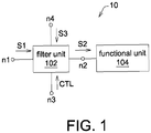
- FIG. 1 shows a block diagram of a circuit for low-noise reference signal generation according to an embodiment of the present invention.
- the circuit 10 includes a filter unit 102 and a functional unit 104.
- the filter unit 102 includes a transistor M and an energy storage component E.
- the transistor M may be a NMOS or a PMOS.
- the transistor M includes a first node n1, a second node n2, a control node n3 and a body node n4.
- the first node n1 of the transistor M is configured to couple to a circuit providing an input signal S1.
- the input signal S1 may be a voltage signal.
- the second node n2 of the transistor M is coupled to the energy storage component E, for providing a filtered signal S2.
- the control node n3 of the transistor M is configured to receive a control signal CTL, and the transistor M is controlled by the control signal CTL to turn on/off.
- the body node n4 of the transistor M is configured to receive a tracking signal S3.
- the tracking signal S3 may be the input signal S1, the filtered signal S2 or a signal which is similar to the input signal S1 or the filtered signal S2.
- the functional unit 104 may be a circuit having high input impedance, e.g. >10G ⁇ , which means that the impedance seen by the filter unit 102 is high enough so that the leakage current from the functional circuit 104 to the filter unit 102 equals to zero or approaches zero.
- the transistor M when the transistor M is turned off by the control signal CTL, the transistor M is equivalent to a resistor having high resistance (e.g., >100M ⁇ ), and the filter unit 102 may act as a RC filter with a resistor having high resistance. Details may be illustrated with referring to a practical example shown in FIG. 2A .
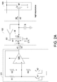
- FIG. 2A shows a practical example of a circuit for low-noise reference signal generation according to an embodiment of the present invention.
- the transistor M is a PMOS
- the energy storage component E can be a MIM (Metal-Insulator-Metal) capacitor, a MOM (Metal-Oxide-Metal) capacitor a MOS capacitor, a MOS varactor (passive capacitor) or a damping circuit (active capacitor).
- the filtered signal S2 is coupled to the body node n4 of the transistor M by an operational amplifier as the tracking signal S3.
- D1 and D2 are junction diodes of the transistor M.
- the functional unit 104 includes a transistor M1 which is a PMOS.
- the input signal is provided by a circuit C1 which includes an operational amplifier OA1, a number of resistors R1 ⁇ R3 and a number of transistors A1, A2.
- the output voltage of the operational amplifier OA1 is input to the filter unit 102 as the input signal S1.
- FIG. 2B shows a damping circuit which is utilized for implementing the energy storage component E.
- the damping circuit 20 includes an operational amplifier 201, a capacitor 203 and a resistor 205.
- An input node n5 of the operational amplifier 201 is configured to couple to the second node n2 of the transistor M.
- One node of the capacitor 203 is coupled to the input node of the operational amplifier 201, and the other node of the capacitor 203 is coupled to an output node of the operational amplifier 201.
- One node of the resistor 205 is coupled to the output node of the operational amplifier 201, and the other node n6 of the resistor 205 is configured to couple to ground, a supply or a reference voltage.
- the operational amplifier 201 of the damping circuit 20 may be implemented in various ways.
- FIGs. 2C and 2D show two circuit examples for implementing the operation amplifier 201. In FIG. 2C , the operational amplifier of the damping circuit 201c is implemented by a NMOS 201c. In FIG. 2D , the operational amplifier of the damping circuit 201d is implemented by a PMOS 201d.
- the equivalent circuit of the filter unit 102 when the transistor M of the filter unit 102 is turned off by the control signal CTL is shown in FIG. 3 .
- the transistor M is equivalent to a resistor Roff which has high resistance.
- the filter circuit 102 is configured as a low pass filter.
- the 3dB frequency of the spectrum of the noise can be adjusted to be lower than an interested band (e.g., 20Hz ⁇ 20kHz). In other words, the energy of the noise within the interested band is reduced. Therefore, it is considered that the input signal S1 is "cleaned" by the filter unit 102, and the filtered signal S2 is generated as a low-noise signal to provide to the functional circuit 104.
- the filtered signal S2 is coupled to the body node n4 of the transistor M, it is possible to avoid generation of leakage current when the transistor M is turned off.
- the filter unit 102 When the transistor M is turned on by the control signal CTL, the filter unit 102 is configured as an all pass filter.
- the input signal S1 can pass through the transistor M and charge the energy storage component E.
- the control signal can be either a digital signal or an analog signal.
- the control signal CTL may be a PWM (pulse width modulation) with regular pulse.
- the control signal CTL is a first voltage level V1 in time interval Tc
- the control signal CTL is a second voltage level V2 in time interval Tf.
- the transistor M is a PMOS
- the transistor M may be turned on during time interval Tc
- the transistor M may be turned off during time interval Tf.
- the first voltage level V1 may be zero and the second voltage V2 may be VDD, but, in an analog case, the first voltage level V1 may have a voltage level higher than zero..
- the energy storage component E may be charged during time interval Tc (i.e., the time interval may also refer to a "charging time"), and the filter unit 102 may configured as an all pass filter.
- the filter unit 102 may be configured as a low pass filter during the time interval Tf.
- the control signal is a PWM signal with irregular pulse.
- the time intervals Tc and Tf are not fixed.
- the time interval Tc can be made longer during initial operation of the circuit 10. As the running time gets longer, the time interval Tc can be reduced.
- the control signal CTL may be a PFM (pulse frequency modulation) signal.
- the time of a single period Tr of the control signal CTL is not fixed.
- the ratio of the first time interval and a single period Tr of the control signal CTL is larger than 100 (i.e., Tr/Tc > 100).
- the ratio of the charging time in a single period and the single period is a random variable.
- the above embodiments are for a case that the transistor M is a PMOS.
- the first voltage level V1 of the control signal CTL in the charging time may be lower than VDD.
- FIG. 4 shows a block diagram of a circuit for low-noise reference signal generation according to another embodiment of the present invention.
- the circuit 40 is similar to the circuit 10, but the circuit 40 further includes an input unit 106.
- the input unit 106 is a current to voltage (I/V) converting circuit
- the functional unit 104 is a voltage to current (V/I) converting circuit. Since the operations and functions of the filter unit 102 is the same as the embodiment described above, it may not be repeated herein.
- FIG. 5A shows a practical example of a circuit for low-noise reference signal generation according to another embodiment of the present invention.
- the input unit 106 includes a current source Ir and a transistor T1.
- the current source Ir generates a noisy reference current
- the transistor T1 converts the noisy reference current to a noisy voltage signal as the input signal S1.
- the filter unit 102 filters the noise of the input signal S1 and then output the filtered signal S2.
- the functional unit 104 includes a transistor T2.
- the transistor T2 receives the filtered signal S2 and converts the filtered signal S2 to a clean reference current Ic.
- FIG. 1 shows a practical example of a circuit for low-noise reference signal generation according to another embodiment of the present invention.
- the transistor M of the filter unit 102, the transistor T1 of the input unit 106 and the transistor T2 of the functional unit 104 are NMOS.
- the type of the transistors may be different.
- the transistor M of the filter unit 102 is PMOS
- the transistor T1 of the input unit 106 and the transistor T2 of the functional unit 104 are NMOS.
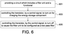
- FIG. 6 shows a flowchart of a method for low-noise reference signal generation according to an embodiment of the present invention.
- step 601 providing a circuit which includes a filter unit and a functional unit is performed.
- the filter unit includes a transistor and an energy storage component.
- the transistor is configured to receive an input signal and output a filtered signal.
- a body node of the transistor is coupled to the input signal, the filtered signal or a signal which is similar to the input signal or the filtered signal.
- the functional unit has high input impedance.
- step 603 controlling the transistor, by a control signal, to turn on for charging the energy storage component is performed.
- the filter unit is configured as an all pass filter.
- step 605 controlling the transistor, by the control signal, to turn off to cause the filter unit to be configured as a low pass filter is performed.
- Steps 603 and 605 may be performed repeatedly during the runtime of the circuit.
- the control signal is a PWM signal or a PFM signal.
- the ratio of a charging time in a single period and the single period may be either fixed or not fixed, wherein the charging time refers to the time interval that the control signal is in a state of first voltage level to turn the transistor on.
- the charging time can be made longer during initial operation of the circuit. As the running time gets longer, the charging time can be reduced.
- the ratio of the charging time in a single period and the single period is larger than 100.
- the ratio of the charging time in a single period and the single period is a random variable.
- a noisy reference signal which is either a reference voltage or a reference current can be cleaned, and a clean reference signal may be produced, within an interested band, for example, 20Hz ⁇ 20kHz in audio use. That is, with the present, the noise of the noisy reference signal within the interest band can be reduced.
Landscapes
- Engineering & Computer Science (AREA)
- Physics & Mathematics (AREA)
- Microelectronics & Electronic Packaging (AREA)
- Nonlinear Science (AREA)
- Electromagnetism (AREA)
- General Physics & Mathematics (AREA)
- Radar, Positioning & Navigation (AREA)
- Automation & Control Theory (AREA)
- Power Engineering (AREA)
- Networks Using Active Elements (AREA)
- Amplifiers (AREA)
Abstract
Description
- The invention relates in general to method and circuit for reference signal generation, and more particular to method and circuit for low-noise signal reference generation.
- In various kinds of circuitry, there is a need to generate reference voltages or reference currents. For example, circuitry of earbuds may include one or more digital to analog converters (DAC), and the inputs of the DACs may be provided by one or more circuits which generate reference signals (e.g., reference currents or reference voltages). In this case, the noise of the reference signals may affect the quality of the output audio. In other words, if the noise of the reference noise can be reduced, the quality of the output audio can be improved. Therefore, how to generate low-noise reference signals has always been a goal of the industry.
- An aspect of the present invention discloses a circuit for low-noise reference signal generation comprising a filter unit and a functional unit. The filter unit comprises a transistor and an energy storage component. The transistor comprises a first node, a second node, a control node and a body node. The first node is configured to receive an input signal. The second node is configured to output a filtered signal. The control node is configured to receive a control signal for controlling the transistor to turn on or off. The body node is configured to couple to the input signal, the output signal or a signal which is similar to the input signal or the output signal. The energy storage component is coupled to the second node of the transistor. The functional unit is coupled to the second node of the transistor and the energy storage component. The functional unit has high input impedance.
- Another aspect of the present invention discloses a circuit for low-noise reference signal generation comprising a filter unit, an input unit and a functional unit. The filter unit comprises a transistor and an energy storage component. The transistor comprises a first node, a second node, a control node and a body node. The first node is configured to receive an input signal. The second node is configured to output a filtered signal. The control node is configured to receive a control signal for controlling the transistor to turn on or off. The body node is configured to couple to the input signal, the output signal or a signal which is similar to the input signal or the output signal. The energy storage component is coupled to the second node of the transistor. The functional unit is coupled to the second node of the transistor and the energy storage component. The input unit is coupled to the first node of the transistor. The input unit is a current to voltage converting circuit. The functional unit is a voltage to current converting circuit which has high input impedance.
- Yet another aspect of the present invention discloses a method for low-noise reference signal generation, comprising: providing a circuit which includes a filter unit and a functional unit, wherein the filter unit includes a transistor and an energy storage component, the transistor is configured to receive an input signal and output a filtered signal, a body node of the transistor is coupled to the input signal, the filtered signal or a signal which is similar to the input signal or the filtered signal, and the functional unit has high input impedance; controlling the transistor, by a control signal, to turn on for charging the energy storage component; and controlling the transistor, by the control signal, to turn off to cause the filter unit to be configured as a low pass filter.
- The above and other aspects of the invention will become better understood with regard to the following detailed description of the preferred but non-limiting embodiment(s). The following description is made with reference to the accompanying drawings.
-
-
FIG. 1 shows a block diagram of a circuit for low-noise reference signal generation according to an embodiment of the present invention. -
FIG. 2A shows a practical example of a circuit for low-noise reference signal generation according to an embodiment of the present invention. -
FIG. 2B shows an example of a damping circuit for implementing the energy storage component.FIGs. 2C and 2D show two circuit examples for implementing the operation amplifier of the damping circuit inFig. 2B . -
FIG. 3 shows an equivalent circuit of the filter unit when the transistor is turned off. -
FIG. 4 shows a block diagram of a circuit for low-noise reference signal generation according to another embodiment of the present invention. -
FIGs. 5A and 5B show practical examples of a circuit for low-noise reference signal generation according to another embodiment of the present invention. -
FIG. 6 shows a flowchart of a method for low-noise reference signal generation according to an embodiment of the present invention. -
FIGs. 7A∼7C show scheme diagrams of control signals for controlling a filter unit according to an embodiment of the present invention. - Referring to
FIG. 1, FIG. 1 shows a block diagram of a circuit for low-noise reference signal generation according to an embodiment of the present invention. Thecircuit 10 includes afilter unit 102 and afunctional unit 104. Thefilter unit 102 includes a transistor M and an energy storage component E. The transistor M may be a NMOS or a PMOS. The transistor M includes a first node n1, a second node n2, a control node n3 and a body node n4. The first node n1 of the transistor M is configured to couple to a circuit providing an input signal S1. The input signal S1 may be a voltage signal. The second node n2 of the transistor M is coupled to the energy storage component E, for providing a filtered signal S2. The control node n3 of the transistor M is configured to receive a control signal CTL, and the transistor M is controlled by the control signal CTL to turn on/off. The body node n4 of the transistor M is configured to receive a tracking signal S3. The tracking signal S3 may be the input signal S1, the filtered signal S2 or a signal which is similar to the input signal S1 or the filtered signal S2. Thefunctional unit 104 may be a circuit having high input impedance, e.g. >10GΩ, which means that the impedance seen by thefilter unit 102 is high enough so that the leakage current from thefunctional circuit 104 to thefilter unit 102 equals to zero or approaches zero. In the embodiment, when the transistor M is turned off by the control signal CTL, the transistor M is equivalent to a resistor having high resistance (e.g., >100MΩ), and thefilter unit 102 may act as a RC filter with a resistor having high resistance. Details may be illustrated with referring to a practical example shown inFIG. 2A . -
FIG. 2A shows a practical example of a circuit for low-noise reference signal generation according to an embodiment of the present invention. In this example, the transistor M is a PMOS, and the energy storage component E can be a MIM (Metal-Insulator-Metal) capacitor, a MOM (Metal-Oxide-Metal) capacitor a MOS capacitor, a MOS varactor (passive capacitor) or a damping circuit (active capacitor). The filtered signal S2 is coupled to the body node n4 of the transistor M by an operational amplifier as the tracking signal S3. D1 and D2 are junction diodes of the transistor M. Thefunctional unit 104 includes a transistor M1 which is a PMOS. The input signal is provided by a circuit C1 which includes an operational amplifier OA1, a number of resistors R1∼R3 and a number of transistors A1, A2. The output voltage of the operational amplifier OA1 is input to thefilter unit 102 as the input signal S1. To be mentioned,FIG. 2B shows a damping circuit which is utilized for implementing the energy storage component E.The damping circuit 20 includes anoperational amplifier 201, acapacitor 203 and aresistor 205. An input node n5 of theoperational amplifier 201 is configured to couple to the second node n2 of the transistor M. One node of thecapacitor 203 is coupled to the input node of theoperational amplifier 201, and the other node of thecapacitor 203 is coupled to an output node of theoperational amplifier 201. One node of theresistor 205 is coupled to the output node of theoperational amplifier 201, and the other node n6 of theresistor 205 is configured to couple to ground, a supply or a reference voltage. Further, theoperational amplifier 201 of the dampingcircuit 20 may be implemented in various ways.FIGs. 2C and 2D show two circuit examples for implementing theoperation amplifier 201. InFIG. 2C , the operational amplifier of the dampingcircuit 201c is implemented by aNMOS 201c.. InFIG. 2D , the operational amplifier of the dampingcircuit 201d is implemented by aPMOS 201d. - In the embodiment shown in
FIG. 2A , the equivalent circuit of thefilter unit 102 when the transistor M of thefilter unit 102 is turned off by the control signal CTL is shown inFIG. 3 . As shown inFIG. 3 , the transistor M is equivalent to a resistor Roff which has high resistance. That is, thefilter circuit 102 is configured as a low pass filter. By thefilter unit 102 being configured as a low pass filter, the 3dB frequency of the spectrum of the noise can be adjusted to be lower than an interested band (e.g., 20Hz∼20kHz). In other words, the energy of the noise within the interested band is reduced. Therefore, it is considered that the input signal S1 is "cleaned" by thefilter unit 102, and the filtered signal S2 is generated as a low-noise signal to provide to thefunctional circuit 104. - To be mentioned, since the filtered signal S2 is coupled to the body node n4 of the transistor M, it is possible to avoid generation of leakage current when the transistor M is turned off.
- When the transistor M is turned on by the control signal CTL, the
filter unit 102 is configured as an all pass filter. The input signal S1 can pass through the transistor M and charge the energy storage component E. - The control signal can be either a digital signal or an analog signal. In an embodiment, as shown in
FIG. 7A , the control signal CTL may be a PWM (pulse width modulation) with regular pulse. In a single period Tr of the control signal CTL, the control signal CTL is a first voltage level V1 in time interval Tc, and the control signal CTL is a second voltage level V2 in time interval Tf. When the transistor M is a PMOS, the transistor M may be turned on during time interval Tc, and the transistor M may be turned off during time interval Tf. In a digital case, the first voltage level V1 may be zero and the second voltage V2 may be VDD, but, in an analog case, the first voltage level V1 may have a voltage level higher than zero.. That is, the energy storage component E may be charged during time interval Tc (i.e., the time interval may also refer to a "charging time"), and thefilter unit 102 may configured as an all pass filter. In the other hand, thefilter unit 102 may be configured as a low pass filter during the time interval Tf. In another embodiment, as shown inFIG. 7B , the control signal is a PWM signal with irregular pulse. In this embodiment, the time intervals Tc and Tf are not fixed. For example, the time interval Tc can be made longer during initial operation of thecircuit 10. As the running time gets longer, the time interval Tc can be reduced. In yet another embodiment, as shown inFIG. 7C , the control signal CTL may be a PFM (pulse frequency modulation) signal. That is, in this embodiment, the time of a single period Tr of the control signal CTL is not fixed. In an embodiment, the ratio of the first time interval and a single period Tr of the control signal CTL is larger than 100 (i.e., Tr/Tc > 100). In another embodiment, the ratio of the charging time in a single period and the single period is a random variable. - The above embodiments are for a case that the transistor M is a PMOS. In a case that the transistor M is a NMOS, the first voltage level V1 of the control signal CTL in the charging time may be lower than VDD.
- Referring to
FIG. 4, FIG. 4 shows a block diagram of a circuit for low-noise reference signal generation according to another embodiment of the present invention. Thecircuit 40 is similar to thecircuit 10, but thecircuit 40 further includes aninput unit 106. In this embodiment, theinput unit 106 is a current to voltage (I/V) converting circuit, and thefunctional unit 104 is a voltage to current (V/I) converting circuit. Since the operations and functions of thefilter unit 102 is the same as the embodiment described above, it may not be repeated herein. -
FIG. 5A shows a practical example of a circuit for low-noise reference signal generation according to another embodiment of the present invention. Theinput unit 106 includes a current source Ir and a transistor T1. The current source Ir generates a noisy reference current, and the transistor T1 converts the noisy reference current to a noisy voltage signal as the input signal S1. Thefilter unit 102 filters the noise of the input signal S1 and then output the filtered signal S2. Thefunctional unit 104 includes a transistor T2. The transistor T2 receives the filtered signal S2 and converts the filtered signal S2 to a clean reference current Ic. In another practical example inFIG. 5B , the transistor M of thefilter unit 102, the transistor T1 of theinput unit 106 and the transistor T2 of thefunctional unit 104 are NMOS. Noted that, in some cases, the type of the transistors may be different. For example, the transistor M of thefilter unit 102 is PMOS, and the transistor T1 of theinput unit 106 and the transistor T2 of thefunctional unit 104 are NMOS. -
FIG. 6 shows a flowchart of a method for low-noise reference signal generation according to an embodiment of the present invention. - In
step 601, providing a circuit which includes a filter unit and a functional unit is performed. The filter unit includes a transistor and an energy storage component. The transistor is configured to receive an input signal and output a filtered signal. A body node of the transistor is coupled to the input signal, the filtered signal or a signal which is similar to the input signal or the filtered signal. The functional unit has high input impedance. - In
step 603, controlling the transistor, by a control signal, to turn on for charging the energy storage component is performed. In this step, the filter unit is configured as an all pass filter. - In
step 605, controlling the transistor, by the control signal, to turn off to cause the filter unit to be configured as a low pass filter is performed. -
Steps - In an embodiment, the control signal is a PWM signal or a PFM signal. When the control signal is a PWM signal, the ratio of a charging time in a single period and the single period may be either fixed or not fixed, wherein the charging time refers to the time interval that the control signal is in a state of first voltage level to turn the transistor on. In an embodiment, the charging time can be made longer during initial operation of the circuit. As the running time gets longer, the charging time can be reduced. In an embodiment, the ratio of the charging time in a single period and the single period is larger than 100. In an embodiment, the ratio of the charging time in a single period and the single period is a random variable.
- With the present invention, a noisy reference signal which is either a reference voltage or a reference current can be cleaned, and a clean reference signal may be produced, within an interested band, for example, 20Hz∼20kHz in audio use. That is, with the present, the noise of the noisy reference signal within the interest band can be reduced.
- While the invention has been described by way of example and in terms of the preferred embodiment (s), it is to be understood that the invention is not limited thereto. On the contrary, it is intended to cover various modifications and similar arrangements and procedures, and the scope of the appended claims therefore should be accorded the broadest interpretation so as to encompass all such modifications and similar arrangements and procedures.
Claims (15)
- A circuit for low-noise reference signal generation (10), comprising:a filter unit (102), comprising a transistor (M) and an energy storage component (E), wherein the transistor (M) comprises a first node (n1), a second node (n2), a control node (n3) and a body node (n4), the first node (n1) is configured to receive a input signal (S1), the second node (n2) is configured to output a filtered signal (S2), the control node (n3) is configured to receive a control signal (CTL) for controlling the transistor (M) to turn on or off, the body node (n4) is configured to couple to the input signal (S1), the output signal (S2) or a signal which is similar to the input signal (S1) or the output signal (S2), and the energy storage component (E) is coupled to the second node (n2) of the transistor (M); anda functional unit (104), coupled to the second node (n2) of the transistor (M) and the energy storage component (E), wherein the functional unit (104) has high input impedance.
- The circuit according to claim 1, wherein the control signal is a PWM signal with regular pulse, a PWM signal with irregular pulse or a PFM signal.
- The circuit according to claim 1 or 2, wherein when the control signal is in a state of a first voltage level, the transistor is turned on, the energy storage component is charged, and the filter unit is configured as an all pass filter; when the control signal is in a state of a second voltage level, the transistor is turned off, and the filter unit is configured as a low pass filter.
- The circuit according to claim 3, wherein the ratio of the time of the control signal in the state of the first voltage level in a single period of the control signal and the single period of the control signal is a random variable.
- The circuit according to claim 3 or 4, wherein the ratio of the time of the control signal in the state of the first voltage level in a single period of the control signal and the single period of the control signal is larger than 100.
- The circuit according to anyone of the claims 3 to 5, wherein the time of the control signal in the state of the first voltage level in a single period of the control signal is made longer during initial operation of the circuit.
- The circuit according to anyone of the claims 1 to 6, wherein the energy storage component includes a MIM, Metal-Insulator-Metal, capacitor, a MOM, Metal-Oxide-Metal, capacitor, a MOS capacitor or a MOS varactor.
- The circuit according to anyone of the claims 1 to 7, wherein the energy storage component includes a damping circuit, including at least one transistor and a capacitor, and preferably wherein the input node of the damping circuit in the energy storage component is coupled to the second node of the transistor in the filter unit.
- The circuit according to anyone of the claims 1 to 8, further comprising:an input unit (106), coupled to the first node (n1) of the transistor (M), wherein the input unit (106) is a current to voltage converting circuit; andwherein the functional unit (104) is a voltage to current converting circuit.
- A method for low-noise reference signal generation, comprising:providing a circuit (10, 40) which includes a filter unit (102) and a functional unit (104), wherein the filter unit (102) includes a transistor (M) and an energy storage component (E), the transistor (M) is configured to receive an input signal (S1) and output a filtered signal (S2), a body node (n4) of the transistor (n4) is coupled to the input signal (S1), the filtered signal (S2) or a signal which is similar to the input signal (S1) or the filtered signal (S2), and the functional unit (104) has high input impedance;controlling the transistor (M), by a control signal (CTL), to turn on for charging the energy storage component (E); andcontrolling the transistor (M), by the control signal (CTL), to turn off to cause the filter unit (102) to be configured as a low pass filter.
- The method according to claim 10, wherein the control signal is a PWM signal with regular pulse, a PWM signal with irregular pulse or a PFM signal.
- The method according to claim 10 or 11, wherein when the control signal is in a state of a first voltage level, the transistor is turned on, the energy storage component is charged, and the filter unit is configured as an all pass filter; when the control signal is in a state of a second voltage level, the transistor is turned off, and the filter unit is configured as a low pass filter.
- The method according to claim 12, wherein the ratio of the time of the control signal in the state of the first voltage level in a single period of the control signal and the single period of the control signal is a random variable.
- The method according to claim 12 or 13, wherein the ratio of the time of the control signal in the state of the first voltage level in a single period of the control signal and the single period of the control signal is larger than 100.
- The method according to anyone of the claims 12 to 14, wherein the time of the control signal in the state of the first voltage level in a single period of the control signal is made longer during initial operation of the circuit.
Applications Claiming Priority (2)
| Application Number | Priority Date | Filing Date | Title |
|---|---|---|---|
| US201762589019P | 2017-11-21 | 2017-11-21 | |
| US16/163,625 US10574212B2 (en) | 2017-11-21 | 2018-10-18 | Method and circuit for low-noise reference signal generation |
Publications (2)
| Publication Number | Publication Date |
|---|---|
| EP3487070A1 true EP3487070A1 (en) | 2019-05-22 |
| EP3487070B1 EP3487070B1 (en) | 2024-09-11 |
Family
ID=64453293
Family Applications (1)
| Application Number | Title | Priority Date | Filing Date |
|---|---|---|---|
| EP18207538.2A Active EP3487070B1 (en) | 2017-11-21 | 2018-11-21 | Method and circuit for low-noise reference signal generation |
Country Status (4)
| Country | Link |
|---|---|
| US (1) | US10574212B2 (en) |
| EP (1) | EP3487070B1 (en) |
| CN (1) | CN110034732A (en) |
| TW (1) | TWI678608B (en) |
Families Citing this family (2)
| Publication number | Priority date | Publication date | Assignee | Title |
|---|---|---|---|---|
| US11496144B2 (en) * | 2020-11-17 | 2022-11-08 | Centaur Technology, Inc. | Droop reference with programmable filter |
| CN115144664B (en) * | 2022-09-02 | 2022-11-25 | 苏州纳芯微电子股份有限公司 | Method and system for measuring chip high-resistance node noise |
Citations (6)
| Publication number | Priority date | Publication date | Assignee | Title |
|---|---|---|---|---|
| US7218170B1 (en) * | 2003-05-23 | 2007-05-15 | Broadcom Corporation | Multi-pole current mirror filter |
| EP2086111A2 (en) * | 2008-01-31 | 2009-08-05 | Interuniversitair Microelektronica Centrum vzw | Large time constant steering circuit and instrumentation amplifier implementing same |
| US20130234688A1 (en) * | 2012-03-12 | 2013-09-12 | Seiko Instruments Inc. | Boosting circuit |
| EP2639666A1 (en) * | 2012-03-16 | 2013-09-18 | ST-Ericsson SA | Low-noise reference voltages distribution circuit |
| EP3026816A1 (en) * | 2014-11-26 | 2016-06-01 | Nxp B.V. | A low-pass filter |
| WO2016093991A1 (en) * | 2014-12-10 | 2016-06-16 | Qualcomm Incorporated | Subthreshold metal oxide semiconductor for large resistance |
Family Cites Families (9)
| Publication number | Priority date | Publication date | Assignee | Title |
|---|---|---|---|---|
| US5572162A (en) | 1995-01-30 | 1996-11-05 | Harris Corporation | Filter with reduced element ratings and method |
| US6208206B1 (en) * | 1999-02-11 | 2001-03-27 | The Hong Kong University Of Science And Technology | Frequency compensation techniques for low-power multistage amplifiers |
| US6597240B1 (en) * | 2001-04-02 | 2003-07-22 | Cirrus Logic, Inc. | Circuits and methods for slew rate control and current limiting in switch-mode systems |
| US6657481B2 (en) | 2002-04-23 | 2003-12-02 | Nokia Corporation | Current mirror circuit |
| US7057450B2 (en) * | 2003-07-30 | 2006-06-06 | Winbond Electronics Corp. | Noise filter for an integrated circuit |
| US7781826B2 (en) * | 2006-11-16 | 2010-08-24 | Alpha & Omega Semiconductor, Ltd. | Circuit configuration and manufacturing processes for vertical transient voltage suppressor (TVS) and EMI filter |
| DE102008040291A1 (en) * | 2008-07-09 | 2010-01-14 | Robert Bosch Gmbh | Audio amplifier and method for reconfiguring an audio amplifier |
| CN102195466B (en) * | 2010-03-02 | 2014-09-17 | 登丰微电子股份有限公司 | Anti-noise switching conversion circuit and its controller |
| TWI623141B (en) | 2012-07-07 | 2018-05-01 | Skyworks Solutions, Inc. | Circuit, device, method and combination thereof related to upper insulator based on RF switch |
-
2018
- 2018-10-18 US US16/163,625 patent/US10574212B2/en active Active
- 2018-11-19 CN CN201811377413.6A patent/CN110034732A/en active Pending
- 2018-11-19 TW TW107141078A patent/TWI678608B/en active
- 2018-11-21 EP EP18207538.2A patent/EP3487070B1/en active Active
Patent Citations (6)
| Publication number | Priority date | Publication date | Assignee | Title |
|---|---|---|---|---|
| US7218170B1 (en) * | 2003-05-23 | 2007-05-15 | Broadcom Corporation | Multi-pole current mirror filter |
| EP2086111A2 (en) * | 2008-01-31 | 2009-08-05 | Interuniversitair Microelektronica Centrum vzw | Large time constant steering circuit and instrumentation amplifier implementing same |
| US20130234688A1 (en) * | 2012-03-12 | 2013-09-12 | Seiko Instruments Inc. | Boosting circuit |
| EP2639666A1 (en) * | 2012-03-16 | 2013-09-18 | ST-Ericsson SA | Low-noise reference voltages distribution circuit |
| EP3026816A1 (en) * | 2014-11-26 | 2016-06-01 | Nxp B.V. | A low-pass filter |
| WO2016093991A1 (en) * | 2014-12-10 | 2016-06-16 | Qualcomm Incorporated | Subthreshold metal oxide semiconductor for large resistance |
Also Published As
| Publication number | Publication date |
|---|---|
| EP3487070B1 (en) | 2024-09-11 |
| US20190158065A1 (en) | 2019-05-23 |
| CN110034732A (en) | 2019-07-19 |
| US10574212B2 (en) | 2020-02-25 |
| TW201925953A (en) | 2019-07-01 |
| TWI678608B (en) | 2019-12-01 |
Similar Documents
| Publication | Publication Date | Title |
|---|---|---|
| US7961047B2 (en) | Switching amplifier | |
| US7839197B2 (en) | Level shift circuit | |
| US6714074B2 (en) | Power amplifier clipping circuit for minimizing output distortion | |
| TWI587625B (en) | Integrated start-up bias boost for dynamic error vector magnitude enhancement | |
| US20100156520A1 (en) | Reference voltage generator | |
| JP2011528870A (en) | Low noise high efficiency bias generation circuit and method | |
| US20090015318A1 (en) | Charge pump drive circuit | |
| US20050140432A1 (en) | Supplying a ramp voltage to an amplifier | |
| US7570116B2 (en) | Output stage | |
| US7151404B2 (en) | Current controlled pulse width modulation circuit and class-D amplifier comprising the same | |
| US7554304B2 (en) | Low dropout voltage regulator for slot-based operation | |
| US7268639B2 (en) | Pulse width modulation circuit | |
| US10574212B2 (en) | Method and circuit for low-noise reference signal generation | |
| US6975164B1 (en) | Method and device for generating constant voltage | |
| US7372324B2 (en) | Digital amplifier | |
| US6310520B1 (en) | High slew-rate operational amplifier architecture | |
| JP2006304013A (en) | Switch circuit | |
| US7227413B1 (en) | Audio amplification device with antipop circuitry | |
| JP2020166648A (en) | Reference voltage generation circuit and semiconductor device | |
| US20120013391A1 (en) | Adaptive bootstrap circuit for controlling cmos switch(es) | |
| CN107968637B (en) | Envelope detection circuit | |
| KR100582172B1 (en) | Class D amplifier | |
| US9985644B1 (en) | Digital to-time converter and method therof | |
| US20080088370A1 (en) | Method, apparatus and system for reducing noise from an amplifier | |
| JP4635724B2 (en) | Charge pump drive circuit |
Legal Events
| Date | Code | Title | Description |
|---|---|---|---|
| PUAI | Public reference made under article 153(3) epc to a published international application that has entered the european phase |
Free format text: ORIGINAL CODE: 0009012 |
|
| STAA | Information on the status of an ep patent application or granted ep patent |
Free format text: STATUS: REQUEST FOR EXAMINATION WAS MADE |
|
| 17P | Request for examination filed |
Effective date: 20181121 |
|
| AK | Designated contracting states |
Kind code of ref document: A1 Designated state(s): AL AT BE BG CH CY CZ DE DK EE ES FI FR GB GR HR HU IE IS IT LI LT LU LV MC MK MT NL NO PL PT RO RS SE SI SK SM TR |
|
| AX | Request for extension of the european patent |
Extension state: BA ME |
|
| RBV | Designated contracting states (corrected) |
Designated state(s): AL AT BE BG CH CY CZ DE DK EE ES FI FR GB GR HR HU IE IS IT LI LT LU LV MC MK MT NL NO PL PT RO RS SE SI SK SM TR |
|
| STAA | Information on the status of an ep patent application or granted ep patent |
Free format text: STATUS: EXAMINATION IS IN PROGRESS |
|
| 17Q | First examination report despatched |
Effective date: 20210709 |
|
| P01 | Opt-out of the competence of the unified patent court (upc) registered |
Effective date: 20230607 |
|
| GRAP | Despatch of communication of intention to grant a patent |
Free format text: ORIGINAL CODE: EPIDOSNIGR1 |
|
| STAA | Information on the status of an ep patent application or granted ep patent |
Free format text: STATUS: GRANT OF PATENT IS INTENDED |
|
| INTG | Intention to grant announced |
Effective date: 20240620 |
|
| GRAS | Grant fee paid |
Free format text: ORIGINAL CODE: EPIDOSNIGR3 |
|
| GRAA | (expected) grant |
Free format text: ORIGINAL CODE: 0009210 |
|
| STAA | Information on the status of an ep patent application or granted ep patent |
Free format text: STATUS: THE PATENT HAS BEEN GRANTED |
|
| AK | Designated contracting states |
Kind code of ref document: B1 Designated state(s): AL AT BE BG CH CY CZ DE DK EE ES FI FR GB GR HR HU IE IS IT LI LT LU LV MC MK MT NL NO PL PT RO RS SE SI SK SM TR |
|
| REG | Reference to a national code |
Ref country code: GB Ref legal event code: FG4D |
|
| REG | Reference to a national code |
Ref country code: CH Ref legal event code: EP |
|
| REG | Reference to a national code |
Ref country code: DE Ref legal event code: R096 Ref document number: 602018074197 Country of ref document: DE |
|
| REG | Reference to a national code |
Ref country code: IE Ref legal event code: FG4D |
|
| REG | Reference to a national code |
Ref country code: LT Ref legal event code: MG9D |
|
| PG25 | Lapsed in a contracting state [announced via postgrant information from national office to epo] |
Ref country code: NO Free format text: LAPSE BECAUSE OF FAILURE TO SUBMIT A TRANSLATION OF THE DESCRIPTION OR TO PAY THE FEE WITHIN THE PRESCRIBED TIME-LIMIT Effective date: 20241211 |
|
| REG | Reference to a national code |
Ref country code: NL Ref legal event code: MP Effective date: 20240911 |
|
| PG25 | Lapsed in a contracting state [announced via postgrant information from national office to epo] |
Ref country code: GR Free format text: LAPSE BECAUSE OF FAILURE TO SUBMIT A TRANSLATION OF THE DESCRIPTION OR TO PAY THE FEE WITHIN THE PRESCRIBED TIME-LIMIT Effective date: 20241212 Ref country code: FI Free format text: LAPSE BECAUSE OF FAILURE TO SUBMIT A TRANSLATION OF THE DESCRIPTION OR TO PAY THE FEE WITHIN THE PRESCRIBED TIME-LIMIT Effective date: 20240911 |
|
| PG25 | Lapsed in a contracting state [announced via postgrant information from national office to epo] |
Ref country code: BG Free format text: LAPSE BECAUSE OF FAILURE TO SUBMIT A TRANSLATION OF THE DESCRIPTION OR TO PAY THE FEE WITHIN THE PRESCRIBED TIME-LIMIT Effective date: 20240911 |
|
| PG25 | Lapsed in a contracting state [announced via postgrant information from national office to epo] |
Ref country code: LV Free format text: LAPSE BECAUSE OF FAILURE TO SUBMIT A TRANSLATION OF THE DESCRIPTION OR TO PAY THE FEE WITHIN THE PRESCRIBED TIME-LIMIT Effective date: 20240911 |
|
| PG25 | Lapsed in a contracting state [announced via postgrant information from national office to epo] |
Ref country code: HR Free format text: LAPSE BECAUSE OF FAILURE TO SUBMIT A TRANSLATION OF THE DESCRIPTION OR TO PAY THE FEE WITHIN THE PRESCRIBED TIME-LIMIT Effective date: 20240911 |
|
| PG25 | Lapsed in a contracting state [announced via postgrant information from national office to epo] |
Ref country code: ES Free format text: LAPSE BECAUSE OF FAILURE TO SUBMIT A TRANSLATION OF THE DESCRIPTION OR TO PAY THE FEE WITHIN THE PRESCRIBED TIME-LIMIT Effective date: 20240911 Ref country code: RS Free format text: LAPSE BECAUSE OF FAILURE TO SUBMIT A TRANSLATION OF THE DESCRIPTION OR TO PAY THE FEE WITHIN THE PRESCRIBED TIME-LIMIT Effective date: 20241211 |
|
| PG25 | Lapsed in a contracting state [announced via postgrant information from national office to epo] |
Ref country code: RS Free format text: LAPSE BECAUSE OF FAILURE TO SUBMIT A TRANSLATION OF THE DESCRIPTION OR TO PAY THE FEE WITHIN THE PRESCRIBED TIME-LIMIT Effective date: 20241211 Ref country code: NO Free format text: LAPSE BECAUSE OF FAILURE TO SUBMIT A TRANSLATION OF THE DESCRIPTION OR TO PAY THE FEE WITHIN THE PRESCRIBED TIME-LIMIT Effective date: 20241211 Ref country code: LV Free format text: LAPSE BECAUSE OF FAILURE TO SUBMIT A TRANSLATION OF THE DESCRIPTION OR TO PAY THE FEE WITHIN THE PRESCRIBED TIME-LIMIT Effective date: 20240911 Ref country code: HR Free format text: LAPSE BECAUSE OF FAILURE TO SUBMIT A TRANSLATION OF THE DESCRIPTION OR TO PAY THE FEE WITHIN THE PRESCRIBED TIME-LIMIT Effective date: 20240911 Ref country code: GR Free format text: LAPSE BECAUSE OF FAILURE TO SUBMIT A TRANSLATION OF THE DESCRIPTION OR TO PAY THE FEE WITHIN THE PRESCRIBED TIME-LIMIT Effective date: 20241212 Ref country code: FI Free format text: LAPSE BECAUSE OF FAILURE TO SUBMIT A TRANSLATION OF THE DESCRIPTION OR TO PAY THE FEE WITHIN THE PRESCRIBED TIME-LIMIT Effective date: 20240911 Ref country code: ES Free format text: LAPSE BECAUSE OF FAILURE TO SUBMIT A TRANSLATION OF THE DESCRIPTION OR TO PAY THE FEE WITHIN THE PRESCRIBED TIME-LIMIT Effective date: 20240911 Ref country code: BG Free format text: LAPSE BECAUSE OF FAILURE TO SUBMIT A TRANSLATION OF THE DESCRIPTION OR TO PAY THE FEE WITHIN THE PRESCRIBED TIME-LIMIT Effective date: 20240911 |
|
| REG | Reference to a national code |
Ref country code: AT Ref legal event code: MK05 Ref document number: 1723583 Country of ref document: AT Kind code of ref document: T Effective date: 20240911 |
|
| PG25 | Lapsed in a contracting state [announced via postgrant information from national office to epo] |
Ref country code: NL Free format text: LAPSE BECAUSE OF FAILURE TO SUBMIT A TRANSLATION OF THE DESCRIPTION OR TO PAY THE FEE WITHIN THE PRESCRIBED TIME-LIMIT Effective date: 20240911 |
|
| PG25 | Lapsed in a contracting state [announced via postgrant information from national office to epo] |
Ref country code: PT Free format text: LAPSE BECAUSE OF FAILURE TO SUBMIT A TRANSLATION OF THE DESCRIPTION OR TO PAY THE FEE WITHIN THE PRESCRIBED TIME-LIMIT Effective date: 20250113 Ref country code: IS Free format text: LAPSE BECAUSE OF FAILURE TO SUBMIT A TRANSLATION OF THE DESCRIPTION OR TO PAY THE FEE WITHIN THE PRESCRIBED TIME-LIMIT Effective date: 20250111 |
|
| PG25 | Lapsed in a contracting state [announced via postgrant information from national office to epo] |
Ref country code: SM Free format text: LAPSE BECAUSE OF FAILURE TO SUBMIT A TRANSLATION OF THE DESCRIPTION OR TO PAY THE FEE WITHIN THE PRESCRIBED TIME-LIMIT Effective date: 20240911 Ref country code: RO Free format text: LAPSE BECAUSE OF FAILURE TO SUBMIT A TRANSLATION OF THE DESCRIPTION OR TO PAY THE FEE WITHIN THE PRESCRIBED TIME-LIMIT Effective date: 20240911 |
|
| PG25 | Lapsed in a contracting state [announced via postgrant information from national office to epo] |
Ref country code: EE Free format text: LAPSE BECAUSE OF FAILURE TO SUBMIT A TRANSLATION OF THE DESCRIPTION OR TO PAY THE FEE WITHIN THE PRESCRIBED TIME-LIMIT Effective date: 20240911 Ref country code: AT Free format text: LAPSE BECAUSE OF FAILURE TO SUBMIT A TRANSLATION OF THE DESCRIPTION OR TO PAY THE FEE WITHIN THE PRESCRIBED TIME-LIMIT Effective date: 20240911 |
|
| PG25 | Lapsed in a contracting state [announced via postgrant information from national office to epo] |
Ref country code: CZ Free format text: LAPSE BECAUSE OF FAILURE TO SUBMIT A TRANSLATION OF THE DESCRIPTION OR TO PAY THE FEE WITHIN THE PRESCRIBED TIME-LIMIT Effective date: 20240911 Ref country code: PL Free format text: LAPSE BECAUSE OF FAILURE TO SUBMIT A TRANSLATION OF THE DESCRIPTION OR TO PAY THE FEE WITHIN THE PRESCRIBED TIME-LIMIT Effective date: 20240911 |
|
| PG25 | Lapsed in a contracting state [announced via postgrant information from national office to epo] |
Ref country code: IT Free format text: LAPSE BECAUSE OF FAILURE TO SUBMIT A TRANSLATION OF THE DESCRIPTION OR TO PAY THE FEE WITHIN THE PRESCRIBED TIME-LIMIT Effective date: 20240911 Ref country code: SK Free format text: LAPSE BECAUSE OF FAILURE TO SUBMIT A TRANSLATION OF THE DESCRIPTION OR TO PAY THE FEE WITHIN THE PRESCRIBED TIME-LIMIT Effective date: 20240911 |
|
| REG | Reference to a national code |
Ref country code: DE Ref legal event code: R097 Ref document number: 602018074197 Country of ref document: DE |
|
| REG | Reference to a national code |
Ref country code: CH Ref legal event code: PL |
|
| PG25 | Lapsed in a contracting state [announced via postgrant information from national office to epo] |
Ref country code: MC Free format text: LAPSE BECAUSE OF FAILURE TO SUBMIT A TRANSLATION OF THE DESCRIPTION OR TO PAY THE FEE WITHIN THE PRESCRIBED TIME-LIMIT Effective date: 20240911 |
|
| PG25 | Lapsed in a contracting state [announced via postgrant information from national office to epo] |
Ref country code: DK Free format text: LAPSE BECAUSE OF FAILURE TO SUBMIT A TRANSLATION OF THE DESCRIPTION OR TO PAY THE FEE WITHIN THE PRESCRIBED TIME-LIMIT Effective date: 20240911 |
|
| PG25 | Lapsed in a contracting state [announced via postgrant information from national office to epo] |
Ref country code: LU Free format text: LAPSE BECAUSE OF NON-PAYMENT OF DUE FEES Effective date: 20241121 |
|
| REG | Reference to a national code |
Ref country code: CH Ref legal event code: PL |
|
| PLBE | No opposition filed within time limit |
Free format text: ORIGINAL CODE: 0009261 |
|
| STAA | Information on the status of an ep patent application or granted ep patent |
Free format text: STATUS: NO OPPOSITION FILED WITHIN TIME LIMIT |
|
| PG25 | Lapsed in a contracting state [announced via postgrant information from national office to epo] |
Ref country code: CH Free format text: LAPSE BECAUSE OF NON-PAYMENT OF DUE FEES Effective date: 20241130 |
|
| 26N | No opposition filed |
Effective date: 20250612 |
|
| REG | Reference to a national code |
Ref country code: BE Ref legal event code: MM Effective date: 20241130 |
|
| PG25 | Lapsed in a contracting state [announced via postgrant information from national office to epo] |
Ref country code: SE Free format text: LAPSE BECAUSE OF FAILURE TO SUBMIT A TRANSLATION OF THE DESCRIPTION OR TO PAY THE FEE WITHIN THE PRESCRIBED TIME-LIMIT Effective date: 20240911 |
|
| PG25 | Lapsed in a contracting state [announced via postgrant information from national office to epo] |
Ref country code: BE Free format text: LAPSE BECAUSE OF NON-PAYMENT OF DUE FEES Effective date: 20241130 |
|
| PGFP | Annual fee paid to national office [announced via postgrant information from national office to epo] |
Ref country code: FR Payment date: 20250908 Year of fee payment: 8 |
|
| PG25 | Lapsed in a contracting state [announced via postgrant information from national office to epo] |
Ref country code: IE Free format text: LAPSE BECAUSE OF NON-PAYMENT OF DUE FEES Effective date: 20241121 |
|
| PGFP | Annual fee paid to national office [announced via postgrant information from national office to epo] |
Ref country code: DE Payment date: 20250923 Year of fee payment: 8 |
|
| PGFP | Annual fee paid to national office [announced via postgrant information from national office to epo] |
Ref country code: GB Payment date: 20251001 Year of fee payment: 8 |
|
| PG25 | Lapsed in a contracting state [announced via postgrant information from national office to epo] |
Ref country code: HU Free format text: LAPSE BECAUSE OF FAILURE TO SUBMIT A TRANSLATION OF THE DESCRIPTION OR TO PAY THE FEE WITHIN THE PRESCRIBED TIME-LIMIT; INVALID AB INITIO Effective date: 20181121 |
|
| PG25 | Lapsed in a contracting state [announced via postgrant information from national office to epo] |
Ref country code: CY Free format text: LAPSE BECAUSE OF FAILURE TO SUBMIT A TRANSLATION OF THE DESCRIPTION OR TO PAY THE FEE WITHIN THE PRESCRIBED TIME-LIMIT; INVALID AB INITIO Effective date: 20181121 |