EP3486961A1 - Composite polymer semiconductor using conjugated polymer and insulator polymer, and method for producing same - Google Patents
Composite polymer semiconductor using conjugated polymer and insulator polymer, and method for producing same Download PDFInfo
- Publication number
- EP3486961A1 EP3486961A1 EP17827945.1A EP17827945A EP3486961A1 EP 3486961 A1 EP3486961 A1 EP 3486961A1 EP 17827945 A EP17827945 A EP 17827945A EP 3486961 A1 EP3486961 A1 EP 3486961A1
- Authority
- EP
- European Patent Office
- Prior art keywords
- polymer
- conjugated
- composite
- composite polymer
- insulating
- Prior art date
- Legal status (The legal status is an assumption and is not a legal conclusion. Google has not performed a legal analysis and makes no representation as to the accuracy of the status listed.)
- Withdrawn
Links
Images




Classifications
-
- H—ELECTRICITY
- H10—SEMICONDUCTOR DEVICES; ELECTRIC SOLID-STATE DEVICES NOT OTHERWISE PROVIDED FOR
- H10K—ORGANIC ELECTRIC SOLID-STATE DEVICES
- H10K10/00—Organic devices specially adapted for rectifying, amplifying, oscillating or switching; Organic capacitors or resistors having potential barriers
- H10K10/40—Organic transistors
- H10K10/46—Field-effect transistors, e.g. organic thin-film transistors [OTFT]
- H10K10/462—Insulated gate field-effect transistors [IGFETs]
- H10K10/484—Insulated gate field-effect transistors [IGFETs] characterised by the channel regions
- H10K10/488—Insulated gate field-effect transistors [IGFETs] characterised by the channel regions the channel region comprising a layer of composite material having interpenetrating or embedded materials, e.g. a mixture of donor and acceptor moieties, that form a bulk heterojunction
-
- B—PERFORMING OPERATIONS; TRANSPORTING
- B32—LAYERED PRODUCTS
- B32B—LAYERED PRODUCTS, i.e. PRODUCTS BUILT-UP OF STRATA OF FLAT OR NON-FLAT, e.g. CELLULAR OR HONEYCOMB, FORM
- B32B27/00—Layered products comprising a layer of synthetic resin
- B32B27/12—Layered products comprising a layer of synthetic resin next to a fibrous or filamentary layer
-
- B—PERFORMING OPERATIONS; TRANSPORTING
- B32—LAYERED PRODUCTS
- B32B—LAYERED PRODUCTS, i.e. PRODUCTS BUILT-UP OF STRATA OF FLAT OR NON-FLAT, e.g. CELLULAR OR HONEYCOMB, FORM
- B32B27/00—Layered products comprising a layer of synthetic resin
- B32B27/28—Layered products comprising a layer of synthetic resin comprising synthetic resins not wholly covered by any one of the sub-groups B32B27/30 - B32B27/42
-
- B—PERFORMING OPERATIONS; TRANSPORTING
- B32—LAYERED PRODUCTS
- B32B—LAYERED PRODUCTS, i.e. PRODUCTS BUILT-UP OF STRATA OF FLAT OR NON-FLAT, e.g. CELLULAR OR HONEYCOMB, FORM
- B32B27/00—Layered products comprising a layer of synthetic resin
- B32B27/30—Layered products comprising a layer of synthetic resin comprising vinyl (co)polymers; comprising acrylic (co)polymers
- B32B27/302—Layered products comprising a layer of synthetic resin comprising vinyl (co)polymers; comprising acrylic (co)polymers comprising aromatic vinyl (co)polymers, e.g. styrenic (co)polymers
-
- B—PERFORMING OPERATIONS; TRANSPORTING
- B32—LAYERED PRODUCTS
- B32B—LAYERED PRODUCTS, i.e. PRODUCTS BUILT-UP OF STRATA OF FLAT OR NON-FLAT, e.g. CELLULAR OR HONEYCOMB, FORM
- B32B5/00—Layered products characterised by the non- homogeneity or physical structure, i.e. comprising a fibrous, filamentary, particulate or foam layer; Layered products characterised by having a layer differing constitutionally or physically in different parts
- B32B5/02—Layered products characterised by the non- homogeneity or physical structure, i.e. comprising a fibrous, filamentary, particulate or foam layer; Layered products characterised by having a layer differing constitutionally or physically in different parts characterised by structural features of a fibrous or filamentary layer
- B32B5/028—Net structure, e.g. spaced apart filaments bonded at the crossing points
-
- C—CHEMISTRY; METALLURGY
- C08—ORGANIC MACROMOLECULAR COMPOUNDS; THEIR PREPARATION OR CHEMICAL WORKING-UP; COMPOSITIONS BASED THEREON
- C08L—COMPOSITIONS OF MACROMOLECULAR COMPOUNDS
- C08L25/00—Compositions of, homopolymers or copolymers of compounds having one or more unsaturated aliphatic radicals, each having only one carbon-to-carbon double bond, and at least one being terminated by an aromatic carbocyclic ring; Compositions of derivatives of such polymers
- C08L25/02—Homopolymers or copolymers of hydrocarbons
- C08L25/04—Homopolymers or copolymers of styrene
- C08L25/06—Polystyrene
-
- C—CHEMISTRY; METALLURGY
- C08—ORGANIC MACROMOLECULAR COMPOUNDS; THEIR PREPARATION OR CHEMICAL WORKING-UP; COMPOSITIONS BASED THEREON
- C08L—COMPOSITIONS OF MACROMOLECULAR COMPOUNDS
- C08L65/00—Compositions of macromolecular compounds obtained by reactions forming a carbon-to-carbon link in the main chain; Compositions of derivatives of such polymers
-
- H—ELECTRICITY
- H10—SEMICONDUCTOR DEVICES; ELECTRIC SOLID-STATE DEVICES NOT OTHERWISE PROVIDED FOR
- H10K—ORGANIC ELECTRIC SOLID-STATE DEVICES
- H10K10/00—Organic devices specially adapted for rectifying, amplifying, oscillating or switching; Organic capacitors or resistors having potential barriers
-
- H—ELECTRICITY
- H10—SEMICONDUCTOR DEVICES; ELECTRIC SOLID-STATE DEVICES NOT OTHERWISE PROVIDED FOR
- H10K—ORGANIC ELECTRIC SOLID-STATE DEVICES
- H10K50/00—Organic light-emitting devices
-
- H—ELECTRICITY
- H10—SEMICONDUCTOR DEVICES; ELECTRIC SOLID-STATE DEVICES NOT OTHERWISE PROVIDED FOR
- H10K—ORGANIC ELECTRIC SOLID-STATE DEVICES
- H10K85/00—Organic materials used in the body or electrodes of devices covered by this subclass
- H10K85/10—Organic polymers or oligomers
- H10K85/111—Organic polymers or oligomers comprising aromatic, heteroaromatic, or aryl chains, e.g. polyaniline, polyphenylene or polyphenylene vinylene
-
- H—ELECTRICITY
- H10—SEMICONDUCTOR DEVICES; ELECTRIC SOLID-STATE DEVICES NOT OTHERWISE PROVIDED FOR
- H10K—ORGANIC ELECTRIC SOLID-STATE DEVICES
- H10K85/00—Organic materials used in the body or electrodes of devices covered by this subclass
- H10K85/10—Organic polymers or oligomers
- H10K85/111—Organic polymers or oligomers comprising aromatic, heteroaromatic, or aryl chains, e.g. polyaniline, polyphenylene or polyphenylene vinylene
- H10K85/113—Heteroaromatic compounds comprising sulfur or selene, e.g. polythiophene
-
- B—PERFORMING OPERATIONS; TRANSPORTING
- B32—LAYERED PRODUCTS
- B32B—LAYERED PRODUCTS, i.e. PRODUCTS BUILT-UP OF STRATA OF FLAT OR NON-FLAT, e.g. CELLULAR OR HONEYCOMB, FORM
- B32B2260/00—Layered product comprising an impregnated, embedded, or bonded layer wherein the layer comprises an impregnation, embedding, or binder material
- B32B2260/02—Composition of the impregnated, bonded or embedded layer
- B32B2260/021—Fibrous or filamentary layer
-
- B—PERFORMING OPERATIONS; TRANSPORTING
- B32—LAYERED PRODUCTS
- B32B—LAYERED PRODUCTS, i.e. PRODUCTS BUILT-UP OF STRATA OF FLAT OR NON-FLAT, e.g. CELLULAR OR HONEYCOMB, FORM
- B32B2260/00—Layered product comprising an impregnated, embedded, or bonded layer wherein the layer comprises an impregnation, embedding, or binder material
- B32B2260/04—Impregnation, embedding, or binder material
- B32B2260/046—Synthetic resin
-
- B—PERFORMING OPERATIONS; TRANSPORTING
- B32—LAYERED PRODUCTS
- B32B—LAYERED PRODUCTS, i.e. PRODUCTS BUILT-UP OF STRATA OF FLAT OR NON-FLAT, e.g. CELLULAR OR HONEYCOMB, FORM
- B32B2307/00—Properties of the layers or laminate
- B32B2307/20—Properties of the layers or laminate having particular electrical or magnetic properties, e.g. piezoelectric
- B32B2307/202—Conductive
-
- B—PERFORMING OPERATIONS; TRANSPORTING
- B32—LAYERED PRODUCTS
- B32B—LAYERED PRODUCTS, i.e. PRODUCTS BUILT-UP OF STRATA OF FLAT OR NON-FLAT, e.g. CELLULAR OR HONEYCOMB, FORM
- B32B2307/00—Properties of the layers or laminate
- B32B2307/20—Properties of the layers or laminate having particular electrical or magnetic properties, e.g. piezoelectric
- B32B2307/206—Insulating
-
- B—PERFORMING OPERATIONS; TRANSPORTING
- B32—LAYERED PRODUCTS
- B32B—LAYERED PRODUCTS, i.e. PRODUCTS BUILT-UP OF STRATA OF FLAT OR NON-FLAT, e.g. CELLULAR OR HONEYCOMB, FORM
- B32B2457/00—Electrical equipment
-
- C—CHEMISTRY; METALLURGY
- C08—ORGANIC MACROMOLECULAR COMPOUNDS; THEIR PREPARATION OR CHEMICAL WORKING-UP; COMPOSITIONS BASED THEREON
- C08L—COMPOSITIONS OF MACROMOLECULAR COMPOUNDS
- C08L2203/00—Applications
- C08L2203/20—Applications use in electrical or conductive gadgets
-
- C—CHEMISTRY; METALLURGY
- C08—ORGANIC MACROMOLECULAR COMPOUNDS; THEIR PREPARATION OR CHEMICAL WORKING-UP; COMPOSITIONS BASED THEREON
- C08L—COMPOSITIONS OF MACROMOLECULAR COMPOUNDS
- C08L2205/00—Polymer mixtures characterised by other features
- C08L2205/14—Polymer mixtures characterised by other features containing polymeric additives characterised by shape
- C08L2205/16—Fibres; Fibrils
-
- H—ELECTRICITY
- H10—SEMICONDUCTOR DEVICES; ELECTRIC SOLID-STATE DEVICES NOT OTHERWISE PROVIDED FOR
- H10K—ORGANIC ELECTRIC SOLID-STATE DEVICES
- H10K50/00—Organic light-emitting devices
- H10K50/30—Organic light-emitting transistors
-
- H—ELECTRICITY
- H10—SEMICONDUCTOR DEVICES; ELECTRIC SOLID-STATE DEVICES NOT OTHERWISE PROVIDED FOR
- H10K—ORGANIC ELECTRIC SOLID-STATE DEVICES
- H10K59/00—Integrated devices, or assemblies of multiple devices, comprising at least one organic light-emitting element covered by group H10K50/00
- H10K59/10—OLED displays
- H10K59/12—Active-matrix OLED [AMOLED] displays
- H10K59/125—Active-matrix OLED [AMOLED] displays including organic TFTs [OTFT]
-
- H—ELECTRICITY
- H10—SEMICONDUCTOR DEVICES; ELECTRIC SOLID-STATE DEVICES NOT OTHERWISE PROVIDED FOR
- H10K—ORGANIC ELECTRIC SOLID-STATE DEVICES
- H10K85/00—Organic materials used in the body or electrodes of devices covered by this subclass
- H10K85/10—Organic polymers or oligomers
- H10K85/111—Organic polymers or oligomers comprising aromatic, heteroaromatic, or aryl chains, e.g. polyaniline, polyphenylene or polyphenylene vinylene
- H10K85/113—Heteroaromatic compounds comprising sulfur or selene, e.g. polythiophene
- H10K85/1135—Polyethylene dioxythiophene [PEDOT]; Derivatives thereof
-
- H—ELECTRICITY
- H10—SEMICONDUCTOR DEVICES; ELECTRIC SOLID-STATE DEVICES NOT OTHERWISE PROVIDED FOR
- H10K—ORGANIC ELECTRIC SOLID-STATE DEVICES
- H10K85/00—Organic materials used in the body or electrodes of devices covered by this subclass
- H10K85/10—Organic polymers or oligomers
- H10K85/151—Copolymers
-
- H—ELECTRICITY
- H10—SEMICONDUCTOR DEVICES; ELECTRIC SOLID-STATE DEVICES NOT OTHERWISE PROVIDED FOR
- H10K—ORGANIC ELECTRIC SOLID-STATE DEVICES
- H10K85/00—Organic materials used in the body or electrodes of devices covered by this subclass
- H10K85/60—Organic compounds having low molecular weight
- H10K85/615—Polycyclic condensed aromatic hydrocarbons, e.g. anthracene
- H10K85/621—Aromatic anhydride or imide compounds, e.g. perylene tetra-carboxylic dianhydride or perylene tetracarboxylic di-imide
Definitions
- the present invention relates to a structure of a composite polymer semiconductor structure and a method of producing the same, and more particularly, to a composite polymer semiconductor formed by mixing a conjugated polymer with an insulating polymer, and a method of producing the same.
- the present invention is directed to providing a structure of a composite polymer semiconductor, which has a mesh shape in which a conjugated polymer and an insulating polymer are bonded, for a transparent and flexible organic electronic device.
- the present invention is also directed to providing a method of producing a composite polymer.
- One aspect of the present invention provides a composite polymer semiconductor including an insulating polymer layer configured to form a matrix and a conjugated polymer layer coexisting with the insulating polymer layer and formed with a fiber structure having a regular molecular arrangement in a mesh shape.
- the conjugated polymer layer may be made of DPP2T, and the insulating polymer layer may be made of polystyrene (PS).
- PS polystyrene
- the insulating polymer layer and the conjugated polymer layer may be mixed with a mass ratio (%) in the range of 70:30 to 95:5 and may be thin-filmed through a solution process.
- the thin-filmed composite polymer may have transmittance in the range of 95% to 99%.
- Another aspect of the present invention provides a method of producing a composite polymer, the method including mixing a first insulating polymer and a second conjugated polymer and forming a third composite polymer having a mesh shape by mixing the first insulating polymer with the second conjugated polymer.
- the first insulating polymer may be polystyrene (PS).
- the second conjugated polymer may be DPP2T.
- the third composite polymer may be produced by mixing the first insulating polymer and the second conjugated polymer with a mass ratio in the range of 70:30 to 95:5.
- the produced composite polymer is a transparent and flexible organic electronic device such that high economic feasibility can be achieved.
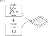
- FIG. 1 shows schematic photographs showing molecular arrangement structures of a conjugated polymer and a produced composite polymer according to one embodiment of the present invention.
- FIG. 1 the photographs showing the molecular arrangement structures of the conjugated polymer and the produced composite polymer are disclosed.
- a substrate is prepared.
- the thin-filmed composite polymer layer is made of an insulating polymer layer forming a matrix and a conjugated polymer layer coexisting with the insulating polymer layer and formed in a mesh shape as a fiber structure with a regular molecular arrangement.
- the substrate may be made of a transparent and flexible polyethylenenaphthalate (PEN) substrate.
- PEN polyethylenenaphthalate
- the composite polymer layer formed on the substrate may have a mesh shape.
- the composite polymer layer may be formed as a thin film by mixing polystyrene (PS) and DPP2T with a mass ratio (%) in the range of 70:30 to 95:5.
- FIG. 1A is a photograph showing a molecular arrangement structure of an original conjugated polymer.
- DPP2T conjugated polymers 100 and 200 a region of DPP2T conjugated polymer 100 having a regular molecular arrangement and a region of DPP2T conjugated polymer 200 having an irregular molecular arrangement are mixed.
- FIG. 1B is a photograph showing a molecular arrangement structure of the thin-filmed composite polymer layer.
- the produced composite polymer layer is formed in a mesh structure.
- the mesh structure formed on the composite polymer layer is constituted with an insulating polymer layer 400 forming a matrix and a conjugated polymer layer 300 coexisting with the insulating polymer layer 400 and formed in a mesh shape as a fiber structure with a regular molecular arrangement.
- the conjugated polymer layer 300 may be formed of DPP2T, and the insulating polymer layer 400 may be formed of PS.
- FIG. 2 is a diagram for describing the composite polymer according to one embodiment of the present invention.
- the first polymer may be a styrene substituted polymer and may include PS, poly( ⁇ -methyl styrene) (PaMS), poly(4-methyl styrene) (P4MS), poly(2-vinylnaphthalene) (PVN), poly(4-vinyl phenol) (PVP), poly(2-vinyl pyridine) (PVPyr), or polyvinyl alcohol (PVA), but the present invention is not limited thereto.
- PS poly( ⁇ -methyl styrene)
- P4MS poly(4-methyl styrene)
- PVN poly(2-vinylnaphthalene)
- PVN poly(4-vinyl phenol)
- PVP poly(2-vinyl pyridine)
- PVA polyvinyl alcohol
- the first polymer may be one selected from various polymers such as polypropylene, poly(methylmethacrylate) (PMMA), poly(vinylacetate) (PVAc), fluoropolymer (Teflon), parylene, polyimide, polycarbonate, poly(vinylphenol) (PVP), polyacetal, polyoxymethylene, polyamide, and the like, but the present is not limited thereto.
- the first polymer may be PS.
- the first polymer and a second polymer are mixed.
- the second polymer may be one selected from among polyacetylene, polyaniline, polypyrrole, polythiophene, and a poly sulfur nitride polymer, but the present invention is not limited thereto.
- the second polymer may be DPP2T.
- the first polymer and the second polymer may be mixed with the mass ratio (%) in the range of 70:30 to 95:5.
- the first polymer and the second polymer are mixed to form a third polymer.
- the third polymer may form a thin film on the substrate by a solution process.
- the third polymer thin-filmed on the substrate forms a mesh structure.
- the substrate may employ a glass substrate or a plastic substrate.
- an organic insulator applicable to a low-temperature solution process may be used.
- the organic insulator may be applied on plastic substrates such as polycarbonate, polysulfone, polyethersulfone, and the like.
- the substrate may employ a PEN substrate made of a flexible material.
- FIG. 3 shows graphs showing absorbance and transmission spectra of the conjugated polymer and the composite polymer according to one embodiment of the present invention.
- FIG. 3 shows absorbance spectra of an original DPP2T polymer and the composite polymer produced according to the present invention.
- the DPP2T polymer has relatively low absorbance in a visible light range due to an intrinsic absorbance characteristic in an infrared light range as compared with conventional polymer semiconductors.
- the DPP2T polymer has high visible light absorbance even in a thin film of less than 10 nm.
- FIG. 3B shows transmittance spectra of the original DPP2T polymer and the composite polymer produced according to present invention.
- the thin-filmed DPP2T polymer exhibits a vivid green color. Meanwhile, when a thin film is formed using the produced composite polymer, it can be confirmed that transmittance in the range of 95% to 99% is exhibited.
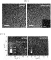
- FIG. 4 shows transmission electron microscope (TEM) images of the conjugated polymer and the produced composite polymer according to one embodiment of the present invention.
- the DPP2T conjugated polymer has a bundle shape of polymer fibers in which an irregular arrangement of crystal structures and an amorphous structure are mixed. Meanwhile, the produced composite polymer has a repeated nano-mesh shape. Further, an image of the composite polymer exhibited as a green color is a result obtained by analyzing the composite polymer with energy dispersive X-ray spectroscopy (EDS). The sulfur element contained in DPP2T was selectively analyzed and the DPP2T was mapped to a green color. Referring to the disclosed green image, a position of a sulfur element contained in only DPP2T is confirmed. Consequently, it can be confirmed that most of the meshes are constituted of DPP2T in the nano-mesh structure of the produced composite polymer.
- EDS energy dispersive X-ray spectroscopy
- FIG. 5 shows graphs, which are obtained through grazing incidence wide angle X-ray scattering (GIWAXS), showing two-dimensional (2D) structures of the conjugated polymer and the produced composite polymer according to one embodiment of the present invention.
- GIWAXS grazing incidence wide angle X-ray scattering
- the DPP2T conjugated polymer in which a portion having a complete crystal structure and an irregular crystal structure are mixed can be confirmed. Meanwhile, the produced composite polymer has a small amount of DPP2T forming a fiber structure in the nano-mesh structure, and thus an apparent crystal structure is not exhibited. This is confirmed by the TEM images of FIG. 4 and the graphs obtained through GIWAXS showing the 2D structures of FIG. 5 .
- FIG. 6 shows graphs showing a transfer characteristic and charge mobility of an FET made of the conjugated polymer and the produced composite polymer according to one embodiment of the present invention.
- a difference in the molecular arrangement structure confirmed through the GIWAXS structure analysis of FIG. 5 is related to a difference in charge transfer characteristic. Therefore, in order to confirm charge transfer characteristics of the conjugated polymer and the produced composite polymer, the FET including the conjugated polymer and the produced composite polymer thin film is produced.
- FIG. 6A is a structural diagram of the FET.
- a substrate is prepared.
- an electrode layer is formed on the substrate.
- a composite polymer semiconductor layer is formed on the electrode layer.
- a gate insulating layer and a gate electrode layer are formed on the composite polymer semiconductor layer.
- the substrate may include a PEN substrate made of a flexible material.
- the electrode layer, the composite polymer semiconductor layer, the gate insulating layer, and the gate electrode layer may be formed of polymers.
- the electrode layer may include PEDOT:PSS and may be formed through ink printing, and the gate insulating layer and the gate electrode layer may be made of amorphous fluorine CYTOP (trade name).
- the conjugated polymer and the produced composite polymer may be thin-filmed through a solution process to form the composite polymer semiconductor layer.
- FIG. 6B is a graph showing charge mobility of the FET including the conjugated polymer and the thin film of the produced composite polymer.
- the charge mobility of the DPP2T conjugated polymer is confirmed as being in the range of 0.1 cm 2 /Vs to 1 cm 2 /Vs. Meanwhile, the charge mobility of the produced composite polymer is confirmed as being in the range of 2.5 cm 2 /Vs to 3.5 cm 2 /Vs. It can be confirmed that the produced composite polymer forms the nano-mesh structure such that a width of a channel region in which charges can flow may be reduced than a width of a channel region of the conjugated polymer, but the charge mobility of the device is improved.
- the channel region of the conjugated polymer and the channel region of the produced composite polymer are converted into a predetermined unit region, it can be seen that the charge mobility of the produced composite polymer is significantly improved to a larger extent than the charge mobility of the conjugated polymer.
- FIG. 6C is a graph showing the charge mobility of the FET including the conjugated polymer and the produced composite polymer according to an electric field and a temperature.
- Activation energy may be calculated using Arrhenius graphs for the temperature and the charge mobility.
- the activation energy refers to energy required for activation before charges move. That is, when a channel through which the charges move is regularly formed, it means that the activation energy is small. Further, it can be confirmed that activation energy of the produced composite polymer is 5 meV, which is much smaller than 19 meV activation energy of the conjugated polymer.
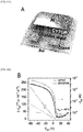
- FIG. 7 shows graphs showing transmittance and a transfer characteristic of a transparent FET which includes the composite polymer according to one embodiment of the present invention and in which all layers are made of polymers.
- FIG. 7 the graphs showing the transmittance and the transfer characteristic of the transparent FET, which includes the composite polymer and in which all the layers are made of polymers, are disclosed.
- FIG. 7A illustrates a transparent FET array which includes the composite polymer and in which all the layers are made of polymers.
- PEDOT:PSS which is a conductive polymer material
- PEN flexible poly(ethylene-2,6-naphthalte)
- FIGS. 7B and 7C are graphs showing charge mobility of the transparent FET including a composite polymer layer. It can be confirmed that charge mobility of the transparent FET including the composite polymer layer has a characteristic of high charge mobility in the range of 0.8 cm 2 /Vs to 1 cm 2 /Vs.
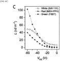
- FIG. 8 shows graphs showing a characteristic of an FET-polymer light-emitting diode (PLED) junction device according to one embodiment of the present invention.
- FIG. 8A shows photographs showing a structure and driving of the FET-PLED junction device.
- FIG. 8B is a graph showing an I-V-L characteristic of an FET-PLED of a yellow color.
- FIG. 8C is a graph showing L-V characteristics of FET-PLEDs of various colors.
- a composite polymer having a mesh structure can be produced using a solution process and combining the insulating polymer to the conjugated polymer with a mass ratio in the range of 70:30 to 95:5.
- the produced composite polymer can improve charge mobility. Further, since a small amount of the conjugated polymer is introduced into the insulating polymer, it is possible to minimize absorbance of visible light such that a transparent and flexible organic electronic device having high economic feasibility can be produced.
Landscapes
- Chemical & Material Sciences (AREA)
- Engineering & Computer Science (AREA)
- Materials Engineering (AREA)
- Medicinal Chemistry (AREA)
- Polymers & Plastics (AREA)
- Organic Chemistry (AREA)
- Health & Medical Sciences (AREA)
- Chemical Kinetics & Catalysis (AREA)
- Composite Materials (AREA)
- Physics & Mathematics (AREA)
- Optics & Photonics (AREA)
- Thin Film Transistor (AREA)
- Compositions Of Macromolecular Compounds (AREA)
- Electroluminescent Light Sources (AREA)
Abstract
Description
- The present invention relates to a structure of a composite polymer semiconductor structure and a method of producing the same, and more particularly, to a composite polymer semiconductor formed by mixing a conjugated polymer with an insulating polymer, and a method of producing the same.
- With the advent of the ubiquitous age, there has been a rapid increase in demand and interest for new devices such as flexible and transparent displays, wearable devices, and the like. As research and development is actively carried out on new electronic devices, organic materials which are inexpensive, applicable to a solution process, and light in weight and flexible are being studied as next generation semiconductors. Research has been carried out on materials based on the existing inorganic materials, so organic polymer semiconductors provide various probabilities as electronic materials. However, the organic polymer semiconductors produced by a solution process have irregular molecular structures and thus most of the organic polymer semiconductors have electrical performances that are much lower than those of the existing inorganic semiconductors.
- In order to solve such problems of the organic polymer semiconductors, a high temperature heat treatment method and a molecular alignment method using a nano-structure have been studied, but these methods are not suitable for commercialization because mass production is impossible. Further, there is a problem to be solved in that it is difficult to apply the existing organic polymer semiconductors on various plastic substrates.
- The present invention is directed to providing a structure of a composite polymer semiconductor, which has a mesh shape in which a conjugated polymer and an insulating polymer are bonded, for a transparent and flexible organic electronic device.
- The present invention is also directed to providing a method of producing a composite polymer.
- One aspect of the present invention provides a composite polymer semiconductor including an insulating polymer layer configured to form a matrix and a conjugated polymer layer coexisting with the insulating polymer layer and formed with a fiber structure having a regular molecular arrangement in a mesh shape.
- The conjugated polymer layer may be made of DPP2T, and the insulating polymer layer may be made of polystyrene (PS).
- The insulating polymer layer and the conjugated polymer layer may be mixed with a mass ratio (%) in the range of 70:30 to 95:5 and may be thin-filmed through a solution process.
- The thin-filmed composite polymer may have transmittance in the range of 95% to 99%.
- Another aspect of the present invention provides a method of producing a composite polymer, the method including mixing a first insulating polymer and a second conjugated polymer and forming a third composite polymer having a mesh shape by mixing the first insulating polymer with the second conjugated polymer.
- In the mixing of the first insulating polymer with the second conjugated polymer, the first insulating polymer may be polystyrene (PS).
- In the mixing of the first insulating polymer with the second conjugated polymer, the second conjugated polymer may be DPP2T.
- In the forming of the third composite polymer having the mesh shape, the third composite polymer may be produced by mixing the first insulating polymer and the second conjugated polymer with a mass ratio in the range of 70:30 to 95:5.
- In accordance with a composite polymer semiconductor having a mesh shape in which a conjugated polymer and an insulating polymer are bonded and a method of producing the same, a solution process is used and a mesh structure is formed such that a produced composite polymer can have high charge mobility.
- Further, a small amount of conjugated polymer is introduced into the insulating polymer such that a transparent and flexible organic electronic device is produced by minimizing absorption of visible light. The produced composite polymer is a transparent and flexible organic electronic device such that high economic feasibility can be achieved.
- It should be noted that effects of the present invention are not limited to the above-described effects, and other effects of the present invention not mentioned above can be clearly understood by those skilled in the art from the following descriptions.
-
-
FIGS. 1A and 1B show schematic photographs showing molecular arrangement structures of a conjugated polymer and a produced composite polymer according to one embodiment of the present invention. -
FIG. 2 is a diagram for describing the composite polymer according to one embodiment of the present invention. -
FIGS. 3A and 3B show graphs showing absorbance and transmission spectra of the conjugated polymer and the produced composite polymer according to one embodiment of the present invention. -
FIG. 4 shows transmission electron microscope (TEM) images of the conjugated polymer and the produced composite polymer according to one embodiment of the present invention. -
FIG. 5 shows graphs, which are obtained through grazing incidence wide angle X-ray scattering (GIWAXS), showing two-dimensional (2D) structures of the conjugated polymer and the produced composite polymer according to one embodiment of the present invention. -
FIGS. 6A to 6C show graphs showing a transfer characteristic and charge mobility of a field effect transistor (FET) made of the conjugated polymer and the produced composite polymer according to one embodiment of the present invention. -
FIGS. 7A to 7C show graphs showing transmittance and a transfer characteristic of a transparent FET which includes the composite polymer according to one embodiment of the present invention and in which all layers are made of polymers. -
FIGS. 8A to 8C show graphs showing a characteristic of an FET-polymer light-emitting diode (PLED) junction device according to one embodiment of the present invention. - Hereinafter, exemplary embodiments of the present invention will be described in detail with reference to the accompanying drawings.
- The exemplary embodiments of the present invention may be modified in various other forms, and the scope of the present invention is not limited to the exemplary embodiments described below. Further, these embodiments are provided to more fully describe the present invention to those skilled in the art. Therefore, shapes and sizes of components in the drawings may be exaggerated for clarity, and components denoted by the same reference numerals in the drawings are the same components.
-
FIG. 1 shows schematic photographs showing molecular arrangement structures of a conjugated polymer and a produced composite polymer according to one embodiment of the present invention. - Referring to
FIG. 1 , the photographs showing the molecular arrangement structures of the conjugated polymer and the produced composite polymer are disclosed. - A substrate is prepared.
- Subsequently, a composite polymer layer which is thin-filmed through a solution process is formed.
- The thin-filmed composite polymer layer is made of an insulating polymer layer forming a matrix and a conjugated polymer layer coexisting with the insulating polymer layer and formed in a mesh shape as a fiber structure with a regular molecular arrangement. Further, the substrate may be made of a transparent and flexible polyethylenenaphthalate (PEN) substrate. Furthermore, the composite polymer layer formed on the substrate may have a mesh shape. The composite polymer layer may be formed as a thin film by mixing polystyrene (PS) and DPP2T with a mass ratio (%) in the range of 70:30 to 95:5.
-
FIG. 1A is a photograph showing a molecular arrangement structure of an original conjugated polymer. - In DPP2T conjugated
polymers polymer 100 having a regular molecular arrangement and a region of DPP2T conjugatedpolymer 200 having an irregular molecular arrangement are mixed. - Meanwhile,
FIG. 1B is a photograph showing a molecular arrangement structure of the thin-filmed composite polymer layer. - The produced composite polymer layer is formed in a mesh structure. The mesh structure formed on the composite polymer layer is constituted with an
insulating polymer layer 400 forming a matrix and a conjugatedpolymer layer 300 coexisting with theinsulating polymer layer 400 and formed in a mesh shape as a fiber structure with a regular molecular arrangement. The conjugatedpolymer layer 300 may be formed of DPP2T, and theinsulating polymer layer 400 may be formed of PS. -
FIG. 2 is a diagram for describing the composite polymer according to one embodiment of the present invention. - Referring to
FIG. 2 , a method of producing a composite polymer is disclosed. - A first polymer is prepared. The first polymer may be a styrene substituted polymer and may include PS, poly(α-methyl styrene) (PaMS), poly(4-methyl styrene) (P4MS), poly(2-vinylnaphthalene) (PVN), poly(4-vinyl phenol) (PVP), poly(2-vinyl pyridine) (PVPyr), or polyvinyl alcohol (PVA), but the present invention is not limited thereto. In addition, the first polymer may be one selected from various polymers such as polypropylene, poly(methylmethacrylate) (PMMA), poly(vinylacetate) (PVAc), fluoropolymer (Teflon), parylene, polyimide, polycarbonate, poly(vinylphenol) (PVP), polyacetal, polyoxymethylene, polyamide, and the like, but the present is not limited thereto. However, the first polymer may be PS.
- The first polymer and a second polymer are mixed. The second polymer may be one selected from among polyacetylene, polyaniline, polypyrrole, polythiophene, and a poly sulfur nitride polymer, but the present invention is not limited thereto. However, the second polymer may be DPP2T.
- The first polymer and the second polymer may be mixed with the mass ratio (%) in the range of 70:30 to 95:5.
- The first polymer and the second polymer are mixed to form a third polymer.
- The third polymer may form a thin film on the substrate by a solution process. The third polymer thin-filmed on the substrate forms a mesh structure. Further, the substrate may employ a glass substrate or a plastic substrate. In this case, an organic insulator applicable to a low-temperature solution process may be used. For example, the organic insulator may be applied on plastic substrates such as polycarbonate, polysulfone, polyethersulfone, and the like. In particular, the substrate may employ a PEN substrate made of a flexible material.
-
FIG. 3 shows graphs showing absorbance and transmission spectra of the conjugated polymer and the composite polymer according to one embodiment of the present invention. - Referring to
FIG. 3 , the graphs showing the absorbance and transmission spectra of the conjugated polymer and the composite polymer are disclosed. The graphs showing the absorbance and transmittance spectra of the DPP2T conjugated polymer and the composite polymer produced according to the present invention are compared.FIG. 3A shows absorbance spectra of an original DPP2T polymer and the composite polymer produced according to the present invention. InFIG. 3A , the DPP2T polymer has relatively low absorbance in a visible light range due to an intrinsic absorbance characteristic in an infrared light range as compared with conventional polymer semiconductors. However, owing to a high optical density, the DPP2T polymer has high visible light absorbance even in a thin film of less than 10 nm. -
FIG. 3B shows transmittance spectra of the original DPP2T polymer and the composite polymer produced according to present invention. InFIG. 3B , the thin-filmed DPP2T polymer exhibits a vivid green color. Meanwhile, when a thin film is formed using the produced composite polymer, it can be confirmed that transmittance in the range of 95% to 99% is exhibited. -
FIG. 4 shows transmission electron microscope (TEM) images of the conjugated polymer and the produced composite polymer according to one embodiment of the present invention. - Referring to
FIG. 4 , the TEM images of the conjugated polymer and the produced composite polymer are disclosed. - The TEM images of the DPP2T conjugated polymer and the composite polymer produced according to the present invention are compared.
- The DPP2T conjugated polymer has a bundle shape of polymer fibers in which an irregular arrangement of crystal structures and an amorphous structure are mixed. Meanwhile, the produced composite polymer has a repeated nano-mesh shape. Further, an image of the composite polymer exhibited as a green color is a result obtained by analyzing the composite polymer with energy dispersive X-ray spectroscopy (EDS). The sulfur element contained in DPP2T was selectively analyzed and the DPP2T was mapped to a green color. Referring to the disclosed green image, a position of a sulfur element contained in only DPP2T is confirmed. Consequently, it can be confirmed that most of the meshes are constituted of DPP2T in the nano-mesh structure of the produced composite polymer.
-
FIG. 5 shows graphs, which are obtained through grazing incidence wide angle X-ray scattering (GIWAXS), showing two-dimensional (2D) structures of the conjugated polymer and the produced composite polymer according to one embodiment of the present invention. - Referring to
FIG. 5 , the graphs obtained through GIWAXS showing 2D structures of the conjugated polymer and the produced composite polymer are disclosed. - As shown in the graphs obtained through GIWAXS showing the 2D structures, the DPP2T conjugated polymer in which a portion having a complete crystal structure and an irregular crystal structure are mixed can be confirmed. Meanwhile, the produced composite polymer has a small amount of DPP2T forming a fiber structure in the nano-mesh structure, and thus an apparent crystal structure is not exhibited. This is confirmed by the TEM images of
FIG. 4 and the graphs obtained through GIWAXS showing the 2D structures ofFIG. 5 . -
FIG. 6 shows graphs showing a transfer characteristic and charge mobility of an FET made of the conjugated polymer and the produced composite polymer according to one embodiment of the present invention. - Referring to
FIG. 6 , the graphs showing the transfer characteristic and the charge mobility of the FET made of the conjugated polymer and the produced composite polymer are disclosed. - A difference in the molecular arrangement structure confirmed through the GIWAXS structure analysis of
FIG. 5 is related to a difference in charge transfer characteristic. Therefore, in order to confirm charge transfer characteristics of the conjugated polymer and the produced composite polymer, the FET including the conjugated polymer and the produced composite polymer thin film is produced. -
FIG. 6A is a structural diagram of the FET. - A substrate is prepared.
- Subsequently, an electrode layer is formed on the substrate.
- A composite polymer semiconductor layer is formed on the electrode layer.
- A gate insulating layer and a gate electrode layer are formed on the composite polymer semiconductor layer.
- In particular, the substrate may include a PEN substrate made of a flexible material. Further, except for the substrate, the electrode layer, the composite polymer semiconductor layer, the gate insulating layer, and the gate electrode layer may be formed of polymers. For example, the electrode layer may include PEDOT:PSS and may be formed through ink printing, and the gate insulating layer and the gate electrode layer may be made of amorphous fluorine CYTOP (trade name). In particular, the conjugated polymer and the produced composite polymer may be thin-filmed through a solution process to form the composite polymer semiconductor layer.
-
FIG. 6B is a graph showing charge mobility of the FET including the conjugated polymer and the thin film of the produced composite polymer. - The charge mobility of the DPP2T conjugated polymer is confirmed as being in the range of 0.1 cm2/Vs to 1 cm2/Vs. Meanwhile, the charge mobility of the produced composite polymer is confirmed as being in the range of 2.5 cm2/Vs to 3.5 cm2/Vs. It can be confirmed that the produced composite polymer forms the nano-mesh structure such that a width of a channel region in which charges can flow may be reduced than a width of a channel region of the conjugated polymer, but the charge mobility of the device is improved. Therefore, when the channel region of the conjugated polymer and the channel region of the produced composite polymer are converted into a predetermined unit region, it can be seen that the charge mobility of the produced composite polymer is significantly improved to a larger extent than the charge mobility of the conjugated polymer.
-
FIG. 6C is a graph showing the charge mobility of the FET including the conjugated polymer and the produced composite polymer according to an electric field and a temperature. Activation energy may be calculated using Arrhenius graphs for the temperature and the charge mobility. The activation energy refers to energy required for activation before charges move. That is, when a channel through which the charges move is regularly formed, it means that the activation energy is small. Further, it can be confirmed that activation energy of the produced composite polymer is 5 meV, which is much smaller than 19 meV activation energy of the conjugated polymer. - Consequently, it can be seen that efficient charge transfer is possible in the nano-mesh structure of the composite polymer mainly formed of DPP2T made of PS rather than the conjugated polymer in which crystalline and the irregular structure coexist. Further, it can be confirmed that as strength of the electric field allowing charges to move decreases, charge mobility in the conjugated polymer decreases, whereas even through the strength of the electric field decreases, charge mobility in the composite polymer is maintained. That is, even when the strength of the electric field increases, it can be confirmed that the produced composite polymer having the mesh structure allows charges to move easily due to the formation of an effective charge transfer channel.
-
FIG. 7 shows graphs showing transmittance and a transfer characteristic of a transparent FET which includes the composite polymer according to one embodiment of the present invention and in which all layers are made of polymers. - Referring to
FIG. 7 , the graphs showing the transmittance and the transfer characteristic of the transparent FET, which includes the composite polymer and in which all the layers are made of polymers, are disclosed.FIG. 7A illustrates a transparent FET array which includes the composite polymer and in which all the layers are made of polymers. Further, in order to prepare a transparent electrode, PEDOT:PSS, which is a conductive polymer material, is printed in an ink-jet manner such that the transparent FET array, in which all the layers are made of polymers undergoing a solution process, is implemented. Four layers including an electrode, an insulator film, and a composite polymer are formed on a flexible poly(ethylene-2,6-naphthalte) (PEN) substrate. Further, an element capable of maintaining transmittance of the flexible PEN substrate is implemented.FIGS. 7B and 7C are graphs showing charge mobility of the transparent FET including a composite polymer layer. It can be confirmed that charge mobility of the transparent FET including the composite polymer layer has a characteristic of high charge mobility in the range of 0.8 cm2/Vs to 1 cm2/Vs. -
FIG. 8 shows graphs showing a characteristic of an FET-polymer light-emitting diode (PLED) junction device according to one embodiment of the present invention. - Referring to
FIG. 8 , the graphs showing the characteristic of the FET-PLED junction device are disclosed. -
FIG. 8A shows photographs showing a structure and driving of the FET-PLED junction device. - Through the graph showing the characteristic of the FET-PLED junction device, it can be confirmed that a space is reduced by directly stacking the transparent FET on the PLED and, at the same time, even when a spectrum of light emitted from the PLED passes through the transparent FET, most of the spectrum of light emitted from the PLED is maintained.
FIG. 8B is a graph showing an I-V-L characteristic of an FET-PLED of a yellow color. Further,FIG. 8C is a graph showing L-V characteristics of FET-PLEDs of various colors. Through the graphs showing the characteristics of the FET-PLEDs ofFIGS. 8B and8C , it can be seen that it is possible to effectively control light of the PLED by adjusting a current flowing to the FET. Further, the FET-PLED junction device may be effectively implemented using various light emission materials. - Therefore, according to a manufacturing method of mixing a conjugated polymer and an insulating polymer, a composite polymer having a mesh structure can be produced using a solution process and combining the insulating polymer to the conjugated polymer with a mass ratio in the range of 70:30 to 95:5. The produced composite polymer can improve charge mobility. Further, since a small amount of the conjugated polymer is introduced into the insulating polymer, it is possible to minimize absorbance of visible light such that a transparent and flexible organic electronic device having high economic feasibility can be produced.
Claims (8)
- A composite polymer semiconductor comprising:an insulating polymer layer configured to form a matrix; anda conjugated polymer layer coexisting with the insulating polymer layer and formed with a fiber structure having a regular molecular arrangement in a mesh shape.
- The composite polymer semiconductor of claim 1, wherein:the conjugated polymer layer is made of DPP2T; andthe insulating polymer layer is made of polystyrene (PS).
- The composite polymer semiconductor of claim 1, wherein the insulating polymer layer and the conjugated polymer layer are mixed with a mass ratio (%) in the range of 70:30 to 95:5 and are thin-filmed through a solution process.
- The composite polymer semiconductor of claim 3, wherein the thin-filmed composite polymer has transmittance in the range of 95% to 99%.
- A method of producing a composite polymer, comprising:mixing a first insulating polymer and a second conjugated polymer; andmixing the first insulating polymer with the second conjugated polymer to form a third composite polymer having a mesh shape.
- The method of claim 5, wherein, in the mixing of the first insulating polymer with the second conjugated polymer, the first insulating polymer includes polystyrene (PS).
- The method of claim 5, wherein, in the mixing of the first insulating polymer with the second conjugated polymer, the second conjugated polymer is DPP2T.
- The method of claim 5, wherein, in the forming of the third composite polymer having the mesh shape, the third composite polymer is produced by mixing the first insulating polymer and the second conjugated polymer with a mass ratio in the range of 70:30 to 95:5.
Applications Claiming Priority (2)
| Application Number | Priority Date | Filing Date | Title |
|---|---|---|---|
| KR1020160088444A KR101730389B1 (en) | 2016-07-13 | 2016-07-13 | Polymer semiconductor composite using insulating polymer and conjugated semiconducting polymer and manufacturing method of the same |
| PCT/KR2017/007456 WO2018012875A1 (en) | 2016-07-13 | 2017-07-13 | Composite polymer semiconductor using conjugated polymer and insulator polymer, and method for producing same |
Publications (2)
| Publication Number | Publication Date |
|---|---|
| EP3486961A1 true EP3486961A1 (en) | 2019-05-22 |
| EP3486961A4 EP3486961A4 (en) | 2020-03-25 |
Family
ID=58704973
Family Applications (1)
| Application Number | Title | Priority Date | Filing Date |
|---|---|---|---|
| EP17827945.1A Withdrawn EP3486961A4 (en) | 2016-07-13 | 2017-07-13 | COMPOSITE POLYMER SEMICONDUCTOR USING A CONJUGATED POLYMER AND AN INSULATING POLYMER, AND METHOD FOR PRODUCING THE SAME |
Country Status (5)
| Country | Link |
|---|---|
| US (1) | US10580990B2 (en) |
| EP (1) | EP3486961A4 (en) |
| JP (1) | JP6732096B2 (en) |
| KR (1) | KR101730389B1 (en) |
| WO (1) | WO2018012875A1 (en) |
Families Citing this family (2)
| Publication number | Priority date | Publication date | Assignee | Title |
|---|---|---|---|---|
| KR101730389B1 (en) * | 2016-07-13 | 2017-04-26 | 광주과학기술원 | Polymer semiconductor composite using insulating polymer and conjugated semiconducting polymer and manufacturing method of the same |
| US11183638B2 (en) * | 2018-05-29 | 2021-11-23 | Purdue Research Foundation | Semiconducting polymer blends for high temperature organic electronics |
Family Cites Families (9)
| Publication number | Priority date | Publication date | Assignee | Title |
|---|---|---|---|---|
| US5408109A (en) | 1991-02-27 | 1995-04-18 | The Regents Of The University Of California | Visible light emitting diodes fabricated from soluble semiconducting polymers |
| JP3776571B2 (en) * | 1997-09-18 | 2006-05-17 | 株式会社東芝 | Functional element |
| GB0612929D0 (en) * | 2006-06-29 | 2006-08-09 | Univ Cambridge Tech | High-performance organic field-effect transistors based on dilute, crystalline-crystalline polymer blends and block copolymers |
| KR20100070652A (en) | 2008-12-18 | 2010-06-28 | 포항공과대학교 산학협력단 | A facile route to flexible all-organic field-effect transistors by all-solution process |
| KR101376494B1 (en) * | 2008-12-18 | 2014-03-19 | 포항공과대학교 산학협력단 | Fabricating low-cost polymer thin-film transistors via formation of semiconducting nanofibrillar network in semiconducting/insulating polymer blends |
| KR101200582B1 (en) | 2010-12-02 | 2012-11-12 | 연세대학교 산학협력단 | Manufacturing method for OTFT using corona discharge |
| EP2764518A1 (en) * | 2011-10-04 | 2014-08-13 | Plextronics, Inc. | Improved doping methods for hole injection and transport layers |
| KR20140103534A (en) | 2013-02-18 | 2014-08-27 | 포항공과대학교 산학협력단 | Field-effect transistor arrray including aligned oxide semiconductor nanowire and a method for fabricating the same |
| KR101730389B1 (en) | 2016-07-13 | 2017-04-26 | 광주과학기술원 | Polymer semiconductor composite using insulating polymer and conjugated semiconducting polymer and manufacturing method of the same |
-
2016
- 2016-07-13 KR KR1020160088444A patent/KR101730389B1/en active Active
-
2017
- 2017-07-13 WO PCT/KR2017/007456 patent/WO2018012875A1/en not_active Ceased
- 2017-07-13 EP EP17827945.1A patent/EP3486961A4/en not_active Withdrawn
- 2017-07-13 JP JP2019501922A patent/JP6732096B2/en active Active
- 2017-07-13 US US16/317,819 patent/US10580990B2/en active Active
Also Published As
| Publication number | Publication date |
|---|---|
| JP2019527931A (en) | 2019-10-03 |
| EP3486961A4 (en) | 2020-03-25 |
| US10580990B2 (en) | 2020-03-03 |
| JP6732096B2 (en) | 2020-07-29 |
| WO2018012875A1 (en) | 2018-01-18 |
| KR101730389B1 (en) | 2017-04-26 |
| US20190237671A1 (en) | 2019-08-01 |
Similar Documents
| Publication | Publication Date | Title |
|---|---|---|
| Younis et al. | Halide perovskites: a new era of solution‐processed electronics | |
| Ni et al. | Recent process of flexible transistor‐structured memory | |
| US11177352B2 (en) | Graphene device, methods of manufacturing and operating the same, and electronic apparatus including the graphene device | |
| US8847313B2 (en) | Transparent electronics based on transfer printed carbon nanotubes on rigid and flexible substrates | |
| Tang et al. | Electronic and photoelectronic memristors based on 2D materials | |
| Son et al. | Flexible organic bistable devices based on graphene embedded in an insulating poly (methyl methacrylate) polymer layer | |
| Lu et al. | Stretchable polymer dielectrics for low-voltage-driven field-effect transistors | |
| Jin et al. | The rise of 2D materials/ferroelectrics for next generation photonics and optoelectronics devices | |
| Yin et al. | Efficient and mechanically robust stretchable organic light-emitting devices by a laser-programmable buckling process | |
| Oh et al. | Graphene/pentacene barristor with ion-gel gate dielectric: flexible ambipolar transistor with high mobility and on/off ratio | |
| Lee et al. | Ultrahigh-mobility and solution-processed inorganic P-channel thin-film transistors based on a transition-metal halide semiconductor | |
| Tseng et al. | Organic transistor memory with a charge storage molecular double-floating-gate monolayer | |
| Nugraha et al. | Enabling ambipolar to heavy n-type transport in PbS quantum dot solids through doping with organic molecules | |
| US8525954B2 (en) | Three-dimensional display article | |
| Li et al. | Photoerasable organic field-effect transistor memory based on a one-step solution-processed hybrid floating gate layer | |
| CN108496413B (en) | Electroluminescent device and method of forming the same | |
| KR20140077230A (en) | Method of manufacturing graphene and the device comprising graphene | |
| US10580990B2 (en) | Composite polymer semiconductor using conjugated polymer and insulator polymer, and method for producing same | |
| Hayakawa et al. | Reconfigurable logic-in-memory constructed using an organic antiambipolar transistor | |
| DE112009000610B4 (en) | Organic thin film transistor and process for its production | |
| Du et al. | Highly sensitive and ultrafast organic phototransistor based on rubrene single crystals | |
| Jeon et al. | Functionalized organic material platform for realization of ternary logic circuit | |
| Kim et al. | Complementary hybrid semiconducting superlattices with multiple channels and mutual stabilization | |
| Sattari-Esfahlan et al. | Flexible graphene-channel memory devices: A review | |
| Zhou et al. | Scalable electronic and optoelectronic devices based on 2D TMDs |
Legal Events
| Date | Code | Title | Description |
|---|---|---|---|
| STAA | Information on the status of an ep patent application or granted ep patent |
Free format text: STATUS: THE INTERNATIONAL PUBLICATION HAS BEEN MADE |
|
| PUAI | Public reference made under article 153(3) epc to a published international application that has entered the european phase |
Free format text: ORIGINAL CODE: 0009012 |
|
| STAA | Information on the status of an ep patent application or granted ep patent |
Free format text: STATUS: REQUEST FOR EXAMINATION WAS MADE |
|
| 17P | Request for examination filed |
Effective date: 20190114 |
|
| AK | Designated contracting states |
Kind code of ref document: A1 Designated state(s): AL AT BE BG CH CY CZ DE DK EE ES FI FR GB GR HR HU IE IS IT LI LT LU LV MC MK MT NL NO PL PT RO RS SE SI SK SM TR |
|
| AX | Request for extension of the european patent |
Extension state: BA ME |
|
| DAV | Request for validation of the european patent (deleted) | ||
| DAX | Request for extension of the european patent (deleted) | ||
| A4 | Supplementary search report drawn up and despatched |
Effective date: 20200220 |
|
| RIC1 | Information provided on ipc code assigned before grant |
Ipc: H01L 51/30 20060101ALN20200215BHEP Ipc: H01L 51/05 20060101AFI20200215BHEP |
|
| STAA | Information on the status of an ep patent application or granted ep patent |
Free format text: STATUS: THE APPLICATION IS DEEMED TO BE WITHDRAWN |
|
| 18D | Application deemed to be withdrawn |
Effective date: 20200922 |