EP3486959A1 - Phosphor device - Google Patents
Phosphor device Download PDFInfo
- Publication number
- EP3486959A1 EP3486959A1 EP18210432.3A EP18210432A EP3486959A1 EP 3486959 A1 EP3486959 A1 EP 3486959A1 EP 18210432 A EP18210432 A EP 18210432A EP 3486959 A1 EP3486959 A1 EP 3486959A1
- Authority
- EP
- European Patent Office
- Prior art keywords
- phosphor
- light
- agent
- color light
- waveband
- Prior art date
- Legal status (The legal status is an assumption and is not a legal conclusion. Google has not performed a legal analysis and makes no representation as to the accuracy of the status listed.)
- Pending
Links
Images






Classifications
-
- G—PHYSICS
- G03—PHOTOGRAPHY; CINEMATOGRAPHY; ANALOGOUS TECHNIQUES USING WAVES OTHER THAN OPTICAL WAVES; ELECTROGRAPHY; HOLOGRAPHY
- G03B—APPARATUS OR ARRANGEMENTS FOR TAKING PHOTOGRAPHS OR FOR PROJECTING OR VIEWING THEM; APPARATUS OR ARRANGEMENTS EMPLOYING ANALOGOUS TECHNIQUES USING WAVES OTHER THAN OPTICAL WAVES; ACCESSORIES THEREFOR
- G03B21/00—Projectors or projection-type viewers; Accessories therefor
- G03B21/14—Details
- G03B21/20—Lamp housings
- G03B21/2006—Lamp housings characterised by the light source
- G03B21/2033—LED or laser light sources
- G03B21/204—LED or laser light sources using secondary light emission, e.g. luminescence or fluorescence
-
- H—ELECTRICITY
- H10—SEMICONDUCTOR DEVICES; ELECTRIC SOLID-STATE DEVICES NOT OTHERWISE PROVIDED FOR
- H10H—INORGANIC LIGHT-EMITTING SEMICONDUCTOR DEVICES HAVING POTENTIAL BARRIERS
- H10H20/00—Individual inorganic light-emitting semiconductor devices having potential barriers, e.g. light-emitting diodes [LED]
- H10H20/80—Constructional details
- H10H20/85—Packages
- H10H20/851—Wavelength conversion means
- H10H20/8515—Wavelength conversion means not being in contact with the bodies
-
- F—MECHANICAL ENGINEERING; LIGHTING; HEATING; WEAPONS; BLASTING
- F21—LIGHTING
- F21V—FUNCTIONAL FEATURES OR DETAILS OF LIGHTING DEVICES OR SYSTEMS THEREOF; STRUCTURAL COMBINATIONS OF LIGHTING DEVICES WITH OTHER ARTICLES, NOT OTHERWISE PROVIDED FOR
- F21V13/00—Producing particular characteristics or distribution of the light emitted by means of a combination of elements specified in two or more of main groups F21V1/00 - F21V11/00
- F21V13/02—Combinations of only two kinds of elements
- F21V13/08—Combinations of only two kinds of elements the elements being filters or photoluminescent elements and reflectors
-
- F—MECHANICAL ENGINEERING; LIGHTING; HEATING; WEAPONS; BLASTING
- F21—LIGHTING
- F21V—FUNCTIONAL FEATURES OR DETAILS OF LIGHTING DEVICES OR SYSTEMS THEREOF; STRUCTURAL COMBINATIONS OF LIGHTING DEVICES WITH OTHER ARTICLES, NOT OTHERWISE PROVIDED FOR
- F21V7/00—Reflectors for light sources
- F21V7/22—Reflectors for light sources characterised by materials, surface treatments or coatings, e.g. dichroic reflectors
- F21V7/28—Reflectors for light sources characterised by materials, surface treatments or coatings, e.g. dichroic reflectors characterised by coatings
- F21V7/30—Reflectors for light sources characterised by materials, surface treatments or coatings, e.g. dichroic reflectors characterised by coatings the coatings comprising photoluminescent substances
-
- F—MECHANICAL ENGINEERING; LIGHTING; HEATING; WEAPONS; BLASTING
- F21—LIGHTING
- F21V—FUNCTIONAL FEATURES OR DETAILS OF LIGHTING DEVICES OR SYSTEMS THEREOF; STRUCTURAL COMBINATIONS OF LIGHTING DEVICES WITH OTHER ARTICLES, NOT OTHERWISE PROVIDED FOR
- F21V9/00—Elements for modifying spectral properties, polarisation or intensity of the light emitted, e.g. filters
- F21V9/30—Elements containing photoluminescent material distinct from or spaced from the light source
- F21V9/32—Elements containing photoluminescent material distinct from or spaced from the light source characterised by the arrangement of the photoluminescent material
-
- F—MECHANICAL ENGINEERING; LIGHTING; HEATING; WEAPONS; BLASTING
- F21—LIGHTING
- F21V—FUNCTIONAL FEATURES OR DETAILS OF LIGHTING DEVICES OR SYSTEMS THEREOF; STRUCTURAL COMBINATIONS OF LIGHTING DEVICES WITH OTHER ARTICLES, NOT OTHERWISE PROVIDED FOR
- F21V9/00—Elements for modifying spectral properties, polarisation or intensity of the light emitted, e.g. filters
- F21V9/30—Elements containing photoluminescent material distinct from or spaced from the light source
- F21V9/38—Combination of two or more photoluminescent elements of different materials
-
- H—ELECTRICITY
- H10—SEMICONDUCTOR DEVICES; ELECTRIC SOLID-STATE DEVICES NOT OTHERWISE PROVIDED FOR
- H10H—INORGANIC LIGHT-EMITTING SEMICONDUCTOR DEVICES HAVING POTENTIAL BARRIERS
- H10H20/00—Individual inorganic light-emitting semiconductor devices having potential barriers, e.g. light-emitting diodes [LED]
- H10H20/80—Constructional details
- H10H20/85—Packages
- H10H20/851—Wavelength conversion means
- H10H20/8514—Wavelength conversion means characterised by their shape, e.g. plate or foil
-
- F—MECHANICAL ENGINEERING; LIGHTING; HEATING; WEAPONS; BLASTING
- F21—LIGHTING
- F21K—NON-ELECTRIC LIGHT SOURCES USING LUMINESCENCE; LIGHT SOURCES USING ELECTROCHEMILUMINESCENCE; LIGHT SOURCES USING CHARGES OF COMBUSTIBLE MATERIAL; LIGHT SOURCES USING SEMICONDUCTOR DEVICES AS LIGHT-GENERATING ELEMENTS; LIGHT SOURCES NOT OTHERWISE PROVIDED FOR
- F21K9/00—Light sources using semiconductor devices as light-generating elements, e.g. using light-emitting diodes [LED] or lasers
- F21K9/60—Optical arrangements integrated in the light source, e.g. for improving the colour rendering index or the light extraction
- F21K9/64—Optical arrangements integrated in the light source, e.g. for improving the colour rendering index or the light extraction using wavelength conversion means distinct or spaced from the light-generating element, e.g. a remote phosphor layer
Definitions
- the present invention relates to a phosphor device, and more particularly to a phosphor device.
- the illumination system of the current projector employs a solid-state light-emitting element (e.g. light emitting diode or laser diode) to replace the conventional high intensity discharge (HID) lamp.
- a solid-state light-emitting element e.g. light emitting diode or laser diode
- the illumination system of the projector may emit three primary color lights, i.e. a red light (R), a green light (G) and a blue light (B).
- a red light (R) a green light
- a blue light (B) a blue light
- the blue solid-state light-emitting element has the highest luminous efficiency. Since the red solid-state light-emitting element and the green solid-state light-emitting element have poor luminous efficiency, the red light or the green light may be produced by using a blue solid-state light-emitting element and a wavelength conversion device (e.g. a phosphor wheel).
- a wavelength conversion device e.g. a phosphor wheel
- the uses of the blue solid-state light-emitting element and the phosphor wheel may directly emit the red light or the green light in replace of the red solid-state light-emitting element or the green solid-state light-emitting element. Consequently, the luminous efficiency of the whole illumination system is enhanced and the manufacturing cost of the illumination system is reduced.
- the present invention provides a phosphor device and a manufacturing method thereof.
- a phosphor layer including a first phosphor agent and a second phosphor agent By utilizing a phosphor layer including a first phosphor agent and a second phosphor agent, the luminous intensity of a color light, which is included in a second waveband light converted by the first phosphor agent, can be increased through the conversion of the second phosphor agent.
- the present invention also provides a phosphor device and a manufacturing method thereof. Since a second phosphor layer including a first phosphor agent and a second phosphor agent is formed behind a first phosphor layer includes only the first phosphor agent along an optical path, most of the energy of a first waveband light is decreased by the first phosphor agent of the first phosphor layer, such that the conversion efficiency of the second phosphor agent is enhanced.
- a phosphor device of an illumination system emitting a first waveband light to the phosphor device so as to be converted into a second waveband light.
- the phosphor device includes a substrate and a first phosphor layer formed on the substrate.
- the first phosphor layer includes a first ingredient and a second ingredient.
- the first waveband light is converted into a first color light and a second color light by the first ingredient.
- the second ingredient is distributed over the first ingredient for converting the first waveband light into a third color light.
- the range of the spectrum of the second color light and the range of the spectrum of the third color light are at least partially overlapped, and the first color light, the second color light and the third color light are integrated as the second waveband light.
- a manufacturing method of a phosphor device includes steps of providing a substrate, and forming a first phosphor layer on the substrate.
- the first phosphor layer includes a first phosphor agent for converting a first waveband light into a second waveband light comprising a first color light and a second color light, and includes a second phosphor agent for converting the first waveband light into the second color light, thereby increasing the luminous intensity of the second color light outputted by the phosphor device.
- FIG. 1A schematically illustrates a phosphor device including a reflective substrate and an illumination system including the phosphor device according to an embodiment of the present invention.
- FIG. 1B schematically illustrates the structure of the phosphor device as shown in FIG. 1A .
- a phosphor device 1 of an illumination system 2 in which the illumination system 2 emits a first waveband light L1
- the first phosphor layer 11 includes a first phosphor agent Y and a second phosphor agent R.
- the first phosphor agent Y is formed on the substrate 10 for converting the first waveband light L1 into a second waveband light L2.
- the second waveband light L2 which could be separated by optical device for projecting, includes a first color light C1 and a second color light C2.
- the second phosphor agent R is distributed over the first phosphor agent Y for converting the first waveband light L1 into the second color light C2 so as to increase the luminous intensity of the second color light C2.
- the first phosphor layer 11 including the first phosphor agent Y and the second phosphor agent R is formed on the substrate 10.
- the second phosphor agent R is utilized for converting the first waveband light L1 into enhancing the second color light C2, thereby increasing the luminous intensity of the second color light C2 outputted by the phosphor device 1.
- the second phosphor agent R can be added in the first phosphor layer 11 with an average distribution or a gradient distribution, such that the second phosphor agent R is distributed over the first phosphor agent Y.
- the second phosphor agent R can be mixed with the first phosphor agent Y as a mixture in a mixing manner.
- the second phosphor agent R and the first phosphor agent Y can be formed as a plurality of segments.
- the segments are for example arranged on the first phosphor layer 11 with a pie-shaped distribution, but not limited thereto.
- the segment each includes the first phosphor agent Y or the second phosphor R, or every one of the segment includes the first phosphor agent Y and the second phosphor agent R simultaneously.
- the first phosphor agent Y is for example a yellow phosphor agent, but not limited thereto.
- the second phosphor agent R is for example a red phosphor agent, but not limited thereto. In some situations, the second phosphor agent R may be a green phosphor agent.
- the primary spirit of the second phosphor agent R is to enhance the intensity and adjust the color saturation level of at least one of the color lights included in the excited light (the second waveband light L2), which is excited by the first phosphor agent Y.
- the symbols (letters) "Y" and "R" are illustrated for indicating the first phosphor agent and the second phosphor agent but not for limiting the colors of the first phosphor agent and the second phosphor agent.
- FIG. 2A schematically illustrates a phosphor device including a transmissive substrate and an illumination system including the phosphor device according to an embodiment of the present invention.
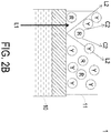
- FIG. 2B schematically illustrates the structure of the phosphor device as shown in FIG. 2A .
- a phosphor device 1 of an illumination system 2 includes a substrate 10 and a first phosphor layer 11.
- the first phosphor layer 11 is similar with the first phosphor layer 11 described in the previous embodiment, and is not redundantly described herein.
- the substrate 10 is a transmissive substrate.
- the phosphor device 1 of the present invention can be considered or realized in another way.
- the first phosphor layer 11 is formed on the substrate and comprising a first ingredient and a second ingredient.
- the first ingredient can be the first phosphor agent, and so does the second ingredient.
- the first waveband light L1 is converted into a first color light C1 and a second color light C2 by the first ingredient.
- the second ingredient is distributed over the first ingredient for converting the first waveband light L1 into a third color light, in which the range of the spectrum of the second color light C2 and the range of the spectrum of the third color light are at least partially overlapped, and the first color light C1, the second color light C2 and the third color light are integrated as the second waveband light L2. Since the range of the spectrum of the second color light C2 and the range of the spectrum of the third color light are at least partially overlapped, at least a portion of the intensity of the second color light C2 is increased.
- the range of the spectrum of the second color light C2 and the range of the spectrum of the third color light are completely overlapped, and the phosphor device 1 meets the embodiments mentioned above. That is, the range of the spectrum of the color light converted by the second ingredient can be selected or adjusted to meet the practical demands but not limited by the embodiments of the present invention.
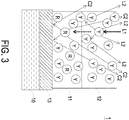
- FIG. 3 schematically illustrates the structure of a phosphor device including a reflective substrate according to an embodiment of the present invention.
- the phosphor device 1 further includes a second phosphor layer 12.
- the substrate 10 is a reflective substrate
- the second phosphor layer 12 is disposed on the first phosphor layer 11.
- the second phosphor layer 12 includes the first phosphor agent Y for converting the first waveband light L1 into the second waveband light L2 and decreasing the energy of the first waveband light L1. That is, when the incident light (i.e. the first waveband light L1) is transmitted through the second phosphor layer 12, a large portion of energy of the incident light is converted.
- the residue power of the first waveband light L1 inputted into the phosphor layer 11 is less than 40 watts, but not limited thereto.
- each of the first phosphor layer 11 and the second phosphor layer 12 is greater than or equal to 10 micrometers (i.e. ⁇ 10 ⁇ m), and less than or equal to 500 micrometers (i.e. ⁇ 500 ⁇ m). In preferred embodiments, the thickness of each of the first phosphor layer 11 and the second phosphor layer 12 is greater than or equal to 50 micrometers (i.e. ⁇ 50 ⁇ m), and less than or equal to 200 micrometers (i.e. ⁇ 200 ⁇ m). It should be noted that the thickness of the first phosphor layer 11 can be equal to or unequal to the thickness of the second phosphor layer 12. In addition, the weight percentage of the second phosphor agent R is less than 85% relative to the first phosphor agent Y.
- the phosphor device 1 of the present invention further includes a reflective coating 13.
- the reflective coating 13 is disposed between the substrate 10 and the first phosphor layer 11 for reflecting at least the second waveband light L2.
- An example of the reflective coating 13 includes but not limited to an all reflective coating, or a dichroic coating. While utilizing a dichroic coating as the reflective coating 13, a color light having the similar range of wavelength with the second waveband light L2 can be reflected by the reflective coating 13. Certainly, the first color light C1 and the second color light C2 both can be reflected by the reflective coating 13. While utilizing a reflective coating, almost all of visible light is reflected by the reflective coating 13.
- the first phosphor layer 11 including the first phosphor agent Y and the second phosphor agent R is formed on the reflective substrate.
- the second phosphor agent R is utilized for converting the first waveband light L1 into the third color light as described above, thereby increasing the luminous intensity of the second color light C2 outputted by the phosphor device 1.
- the second phosphor layer 12 is formed on the first phosphor layer 11.
- the second phosphor layer 12 includes the first phosphor agent Y for converting the first waveband light L1 into the second waveband light L2 and decreasing the energy of the first waveband light L1.
- the reflective coating 13 can be pre-coated on the substrate 10, or be formed on the substrate while processing the manufacturing method.
- FIG. 4 schematically illustrates the structure of a phosphor device including a transmissive substrate according to an embodiment of the present invention.
- the phosphor device 1 further includes a second phosphor layer 12.
- the substrate 10 is a transmissive substrate, and the second phosphor layer 12 is disposed between the first phosphor layer 11 and the substrate 10.
- the second phosphor layer 12 includes the first phosphor agent Y for converting the first waveband light L1 into the second waveband light L2 and decreasing the energy of the first waveband light L1 simultaneously. That is, when the incident light (i.e. the first waveband light L1) is transmitted through the second phosphor layer 12, a large portion of energy of the incident light is converted.
- the residue power of the first waveband light L1 inputted into the phosphor layer 11 is less than 40 watts, but not limited thereto.
- each of the first phosphor layer 11 and the second phosphor layer 12 is greater than or equal to 10 micrometers, and less than or equal to 500 micrometers. In preferred embodiments, the thickness of each of the first phosphor layer 11 and the second phosphor layer 12 is greater than or equal to 50 micrometers, and less than or equal to 200 micrometers.
- the weight percentage of the second phosphor agent R is less than 85% relative to the first phosphor agent Y.
- the phosphor device 1 of the present invention further includes a reflective coating 13.
- the reflective coating 13 is disposed between the substrate 10 and the second phosphor layer 12 for reflecting the second waveband light L2.
- An example of the reflective coating 13 includes but not limited to a dichroic coating. While utilizing a dichroic coating as the reflective coating 13, a color light having the similar range of wavelength with the first waveband light L1 can be passed through the reflective coating 13, and a color light having the similar range of wavelength with the second waveband light L2 can be reflected by the reflective coating 13.
- the second phosphor layer 12 including the first phosphor agent Y is formed on the transmissive substrate.
- the first phosphor layer 11 is then formed on the second phosphor layer 12.
- the first phosphor layer 11 includes the first phosphor agent Y for converting the first waveband light L1 into the second waveband light L2, and the second waveband light L2 comprises a first color light C1 and a second color light C2.
- the second phosphor agent R is added in the first phosphor layer 11 for converting the first waveband light L1 into the second color light C2, thereby increasing the luminous intensity of the second color light C2 outputted by the phosphor device 1.
- the reflective coating 13 can be pre-coated on the substrate 10, or be formed on the substrate while processing the manufacturing method.
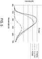
- FIG. 5 schematically illustrates an intensity-wavelength diagram of visible lights of a phosphor device including a yellow phosphor agent as the second phosphor layer 12, and a yellow phosphor agent mixed with a red phosphor agent as the second phosphor layer 11 of the present invention. It is the comparison with a phosphor device utilizing a yellow phosphor agent and a phosphor device utilizing a red phosphor agent of prior art.
- FIG. 5 indicates that the intensities of red light (in the R-Color region) of the phosphor device 1 of the present invention shown in FIG. 3 (i.e.
- the intensity of red light of the phosphor device 1 of the present invention is greater the one of prior art.
- the following Table I illustrates a comparison data.
- the weight percentage of the second phosphor agent R is 25% relative to the first phosphor agent Y.
- the intensity of red light of the phosphor device utilizing a yellow phosphor agent of prior art is assumed as 100% for being the base of the comparison.
- FIG. 6A schematically illustrates a phosphor device including a reflective substrate and an illumination system including the phosphor device according to an embodiment of the present invention.
- FIG. 6B schematically illustrates the structure of the phosphor device as shown in FIG. 6A .
- a phosphor device 3 including a reflective substrate of an illumination system 4 is disclosed herein.
- the illumination system 4 emits a first waveband light L1 along an optical path P.
- the phosphor device 3 includes a substrate 30, a first phosphor layer 31 and a second phosphor layer 32.
- the substrate 30 is disposed on the optical path P.
- the first phosphor layer 31 is formed on a side of the substrate 30.
- the second phosphor layer 32 is formed behind the first phosphor layer 31 along the optical path P.
- the first phosphor layer 31 includes a first phosphor agent Y and x weight percent (i.e. x wt%) of a second phosphor agent R.
- the second phosphor layer 32 includes the first phosphor agent Y and y weight percent (i.e. y wt%) of the second phosphor agent R, and y is greater than x (y>x).
- the first waveband light L1 is converted into a second waveband light L2 by the first phosphor agent Y.
- the second waveband light L2 includes a first color light C1 and a second color light C2.
- the first waveband light L1 is converted into the second color light C2 by the second phosphor agent R, thereby increasing the luminous intensity of the second color light C2.
- x is greater than 0, and y is less than 85.
- the relationship between x and y is given by 0 ⁇ x ⁇ y ⁇ 85. That is, the first phosphor layer 31 and the second phosphor layer 32 each includes a specific weight percent of the second phosphor agent R for converting the first waveband light L1 into the second color light C2 in range of 0-85, and the weight concentration of the second phosphor agent R of the second phosphor layer 32 is greater than the weight concentration of the second phosphor agent R of the first phosphor layer 31.
- the first phosphor layer 31 is disposed for mainly decreasing the energy of the first waveband light.
- each of the first phosphor layer 31 and the second phosphor layer 32 is greater than or equal to 10 micrometers, and less than or equal to 500 micrometers. In preferred embodiments, the thickness of each of the first phosphor layer 31 and the second phosphor layer 32 is greater than or equal to 50 micrometers, and less than or equal to 200 micrometers.
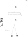
- FIG. 7A schematically illustrates a phosphor device including a transmissive substrate and an illumination system including the phosphor device according to an embodiment of the present invention.
- FIG. 7B schematically illustrates the structure of the phosphor device as shown in FIG. 7A .
- a phosphor device 3 including a transmissive substrate of an illumination system 4 is disclosed herein.
- the illumination system 4 emits a first waveband light L1 along an optical path P.
- the phosphor device 3 includes a substrate 30, a first phosphor layer 31 and a second phosphor layer 32.
- the substrate 30, the first phosphor layer 31 and the second phosphor layer 32 are similar with the above-mentioned embodiment shown in FIGs.
- the substrate 30 shown in FIG. 6B is a reflective substrate
- the substrate 30 shown in FIG. 7B is a transmissive substrate.
- Table II illustrates a comparison data.
- the intensity of red light of the phosphor device utilizing a red phosphor agent of prior art is assumed as 100% for being the base of the comparison.
- Table II L1 Power (Watts) Intensity of red light (Y) Intensity of red light (R) Intensity of red light (Y on Y+25wt%R) Intensity of red light (Y+3.3wt%R on Y+25wt%R) 25 84.9% 100.0% 102.1 % 109.8% 76 119.0% 100.0% 138.5% 138.8% 102 134.0% 100.0% 154.3% 151.2% 152 162.7% 100.0% 182.5% 173.6%
- the present invention provides a phosphor device and a manufacturing method thereof.
- a phosphor layer including a first phosphor agent and a second phosphor agent By utilizing a phosphor layer including a first phosphor agent and a second phosphor agent, the luminous intensity of a color light, which is included in a second waveband light converted by the first phosphor agent, can be increased through the conversion of the second phosphor agent.
- a second phosphor layer including a first phosphor agent and a second phosphor agent is formed behind a first phosphor layer includes only the first phosphor agent along an optical path, most of the energy of a first waveband light is decreased by the first phosphor agent of the first phosphor layer, such that the conversion efficiency of the second phosphor agent is enhanced.
- a phosphor device 1, 3 of an illumination system 2, 4 which emits a first waveband light L1, including a substrate 10, 30 and a first phosphor layer 11, 31.
- the first phosphor layer 11, 31 includes a first phosphor agent Y and a second phosphor agent R.
- the first phosphor agent Y is formed on the substrate 10, 30 for converting the first waveband light L1 into a second waveband light L2.
- the second waveband light L2 comprises a first color light C1 and a second color light C2.
- the second phosphor agent R is distributed over the first phosphor agent Y for converting the first waveband light L1 into the second color light C2 so as to increase the luminous intensity of the second color light C2. Therefore, the luminous intensity of the second color light C2 can be effectively increased.
Landscapes
- Physics & Mathematics (AREA)
- Engineering & Computer Science (AREA)
- Spectroscopy & Molecular Physics (AREA)
- General Engineering & Computer Science (AREA)
- Multimedia (AREA)
- Optics & Photonics (AREA)
- General Physics & Mathematics (AREA)
- Led Device Packages (AREA)
- Projection Apparatus (AREA)
- Investigating, Analyzing Materials By Fluorescence Or Luminescence (AREA)
Abstract
Description
- The present invention relates to a phosphor device, and more particularly to a phosphor device.
- In recent years, a variety of projectors have been widely used in various video applications. For example, projectors can be used for making presentations, holding meetings or giving lectures in classrooms, boardrooms, conference rooms or home theaters. By the projector, an image signal from an image signal source can be enlarged and shown on a display screen. For reducing power consumption and overall volume, the illumination system of the current projector employs a solid-state light-emitting element (e.g. light emitting diode or laser diode) to replace the conventional high intensity discharge (HID) lamp.
- Generally, the illumination system of the projector may emit three primary color lights, i.e. a red light (R), a green light (G) and a blue light (B). Among three primary color solid-state light-emitting elements including a red solid-state light-emitting element, a green solid-state light-emitting element and a blue solid-state light-emitting element, the blue solid-state light-emitting element has the highest luminous efficiency. Since the red solid-state light-emitting element and the green solid-state light-emitting element have poor luminous efficiency, the red light or the green light may be produced by using a blue solid-state light-emitting element and a wavelength conversion device (e.g. a phosphor wheel). That is, the uses of the blue solid-state light-emitting element and the phosphor wheel may directly emit the red light or the green light in replace of the red solid-state light-emitting element or the green solid-state light-emitting element. Consequently, the luminous efficiency of the whole illumination system is enhanced and the manufacturing cost of the illumination system is reduced.
- However, it still has some drawbacks of using a solid-state light-emitting element to emit an exciting light and a phosphor wheel to convert the wavelength of the exciting light. When using a solid-state light-emitting element and a phosphor wheel coated with a phosphor agent to emit an excited light to be separated as color lights for projecting, the luminous intensity or the saturation level of a color light may be not enough.
- Therefore, there is a need of providing an improved illumination system and an improved projection apparatus in order to eliminate the above drawbacks.
- It is an object of the present invention to provide a phosphor device and a manufacturing method thereof for overcoming at least one of the above-mentioned drawbacks encountered by the prior arts.
- The present invention provides a phosphor device and a manufacturing method thereof. By utilizing a phosphor layer including a first phosphor agent and a second phosphor agent, the luminous intensity of a color light, which is included in a second waveband light converted by the first phosphor agent, can be increased through the conversion of the second phosphor agent.
- The present invention also provides a phosphor device and a manufacturing method thereof. Since a second phosphor layer including a first phosphor agent and a second phosphor agent is formed behind a first phosphor layer includes only the first phosphor agent along an optical path, most of the energy of a first waveband light is decreased by the first phosphor agent of the first phosphor layer, such that the conversion efficiency of the second phosphor agent is enhanced.
- In accordance with an aspect of the present invention, there is provided a phosphor device of an illumination system emitting a first waveband light to the phosphor device so as to be converted into a second waveband light. The phosphor device includes a substrate and a first phosphor layer formed on the substrate. The first phosphor layer includes a first ingredient and a second ingredient. The first waveband light is converted into a first color light and a second color light by the first ingredient. The second ingredient is distributed over the first ingredient for converting the first waveband light into a third color light. The range of the spectrum of the second color light and the range of the spectrum of the third color light are at least partially overlapped, and the first color light, the second color light and the third color light are integrated as the second waveband light.
- In accordance with a further aspect of the present invention, there is provided a manufacturing method of a phosphor device. The manufacturing method includes steps of providing a substrate, and forming a first phosphor layer on the substrate. The first phosphor layer includes a first phosphor agent for converting a first waveband light into a second waveband light comprising a first color light and a second color light, and includes a second phosphor agent for converting the first waveband light into the second color light, thereby increasing the luminous intensity of the second color light outputted by the phosphor device.
- The above contents of the present invention will become more readily apparent to those ordinarily skilled in the art after reviewing the following detailed description and accompanying drawings, in which:
-
-
FIG. 1A schematically illustrates a phosphor device including a reflective substrate and an illumination system including the phosphor device according to an embodiment of the present invention; -
FIG. 1B schematically illustrates the structure of the phosphor device as shown inFIG. 1A ; -
FIG. 2A schematically illustrates a phosphor device including a transmissive substrate and an illumination system including the phosphor device according to an embodiment of the present invention; -
FIG. 2B schematically illustrates the structure of the phosphor device as shown inFIG. 2A ; -
FIG. 3 schematically illustrates the structure of a phosphor device including a reflective substrate according to an embodiment of the present invention; -
FIG. 4 schematically illustrates the structure of a phosphor device including a transmissive substrate according to an embodiment of the present invention; -
FIG. 5 schematically illustrates an intensity-wavelength diagram of visible lights of a phosphor device including a yellow phosphor agent and a red phosphor agent of the present invention, and a phosphor device utilizing a yellow phosphor agent and a phosphor device utilizing a red phosphor agent of prior art; -
FIG. 6A schematically illustrates a phosphor device including a reflective substrate and an illumination system including the phosphor device according to an embodiment of the present invention; -
FIG. 6B schematically illustrates the structure of the phosphor device as shown inFIG. 6A ; -
FIG. 7A schematically illustrates a phosphor device including a transmissive substrate and an illumination system including the phosphor device according to an embodiment of the present invention; and -
FIG. 7B schematically illustrates the structure of the phosphor device as shown inFIG. 7A . - The present invention will now be described more specifically with reference to the following embodiments. It is to be noted that the following descriptions of preferred embodiments of this invention are presented herein for purpose of illustration and description only. It is not intended to be exhaustive or to be limited to the precise form disclosed.
-
FIG. 1A schematically illustrates a phosphor device including a reflective substrate and an illumination system including the phosphor device according to an embodiment of the present invention.FIG. 1B schematically illustrates the structure of the phosphor device as shown inFIG. 1A . As shown inFIG. 1A andFIG. 1B , aphosphor device 1 of anillumination system 2, in which theillumination system 2 emits a first waveband light L1, includes asubstrate 10 and afirst phosphor layer 11. Thefirst phosphor layer 11 includes a first phosphor agent Y and a second phosphor agent R. The first phosphor agent Y is formed on thesubstrate 10 for converting the first waveband light L1 into a second waveband light L2. The second waveband light L2, which could be separated by optical device for projecting, includes a first color light C1 and a second color light C2. The second phosphor agent R is distributed over the first phosphor agent Y for converting the first waveband light L1 into the second color light C2 so as to increase the luminous intensity of the second color light C2. - It should be noted that in a manufacturing method of the
phosphor device 1, after thesubstrate 10 is provided, thefirst phosphor layer 11 including the first phosphor agent Y and the second phosphor agent R is formed on thesubstrate 10. The second phosphor agent R is utilized for converting the first waveband light L1 into enhancing the second color light C2, thereby increasing the luminous intensity of the second color light C2 outputted by thephosphor device 1. The second phosphor agent R can be added in thefirst phosphor layer 11 with an average distribution or a gradient distribution, such that the second phosphor agent R is distributed over the first phosphor agent Y. Certainly, the second phosphor agent R can be mixed with the first phosphor agent Y as a mixture in a mixing manner. Alternatively, the second phosphor agent R and the first phosphor agent Y can be formed as a plurality of segments. The segments are for example arranged on thefirst phosphor layer 11 with a pie-shaped distribution, but not limited thereto. The segment each includes the first phosphor agent Y or the second phosphor R, or every one of the segment includes the first phosphor agent Y and the second phosphor agent R simultaneously. - In this embodiment and the following embodiments, the first phosphor agent Y is for example a yellow phosphor agent, but not limited thereto. Meanwhile, the second phosphor agent R is for example a red phosphor agent, but not limited thereto. In some situations, the second phosphor agent R may be a green phosphor agent. The primary spirit of the second phosphor agent R is to enhance the intensity and adjust the color saturation level of at least one of the color lights included in the excited light (the second waveband light L2), which is excited by the first phosphor agent Y. Furthermore, the symbols (letters) "Y" and "R" are illustrated for indicating the first phosphor agent and the second phosphor agent but not for limiting the colors of the first phosphor agent and the second phosphor agent.
-
FIG. 2A schematically illustrates a phosphor device including a transmissive substrate and an illumination system including the phosphor device according to an embodiment of the present invention.FIG. 2B schematically illustrates the structure of the phosphor device as shown inFIG. 2A . As shown inFIG. 2A andFIG. 2B , aphosphor device 1 of anillumination system 2 includes asubstrate 10 and afirst phosphor layer 11. Thefirst phosphor layer 11 is similar with thefirst phosphor layer 11 described in the previous embodiment, and is not redundantly described herein. In this embodiment, thesubstrate 10 is a transmissive substrate. - It should be noted that the
phosphor device 1 of the present invention can be considered or realized in another way. In an embodiment, thefirst phosphor layer 11 is formed on the substrate and comprising a first ingredient and a second ingredient. The first ingredient can be the first phosphor agent, and so does the second ingredient. Furthermore, the first waveband light L1 is converted into a first color light C1 and a second color light C2 by the first ingredient. The second ingredient is distributed over the first ingredient for converting the first waveband light L1 into a third color light, in which the range of the spectrum of the second color light C2 and the range of the spectrum of the third color light are at least partially overlapped, and the first color light C1, the second color light C2 and the third color light are integrated as the second waveband light L2. Since the range of the spectrum of the second color light C2 and the range of the spectrum of the third color light are at least partially overlapped, at least a portion of the intensity of the second color light C2 is increased. - On the other hand, when the third color light converted by the second ingredient is similar with the second color light C2 converted by the first ingredient, the range of the spectrum of the second color light C2 and the range of the spectrum of the third color light are completely overlapped, and the
phosphor device 1 meets the embodiments mentioned above. That is, the range of the spectrum of the color light converted by the second ingredient can be selected or adjusted to meet the practical demands but not limited by the embodiments of the present invention. -
FIG. 3 schematically illustrates the structure of a phosphor device including a reflective substrate according to an embodiment of the present invention. As shown inFIG. 1B andFIG. 3 , thephosphor device 1 further includes asecond phosphor layer 12. In some embodiments, thesubstrate 10 is a reflective substrate, and thesecond phosphor layer 12 is disposed on thefirst phosphor layer 11. Thesecond phosphor layer 12 includes the first phosphor agent Y for converting the first waveband light L1 into the second waveband light L2 and decreasing the energy of the first waveband light L1. That is, when the incident light (i.e. the first waveband light L1) is transmitted through thesecond phosphor layer 12, a large portion of energy of the incident light is converted. For example, the residue power of the first waveband light L1 inputted into thephosphor layer 11 is less than 40 watts, but not limited thereto. - The thickness of each of the
first phosphor layer 11 and thesecond phosphor layer 12 is greater than or equal to 10 micrometers (i.e. ≥10 µm), and less than or equal to 500 micrometers (i.e. ≤500 µm). In preferred embodiments, the thickness of each of thefirst phosphor layer 11 and thesecond phosphor layer 12 is greater than or equal to 50 micrometers (i.e. ≥50 µm), and less than or equal to 200 micrometers (i.e. ≤200 µm). It should be noted that the thickness of thefirst phosphor layer 11 can be equal to or unequal to the thickness of thesecond phosphor layer 12. In addition, the weight percentage of the second phosphor agent R is less than 85% relative to the first phosphor agent Y. - In this embodiment, the
phosphor device 1 of the present invention further includes areflective coating 13. Thereflective coating 13 is disposed between thesubstrate 10 and thefirst phosphor layer 11 for reflecting at least the second waveband light L2. An example of thereflective coating 13 includes but not limited to an all reflective coating, or a dichroic coating. While utilizing a dichroic coating as thereflective coating 13, a color light having the similar range of wavelength with the second waveband light L2 can be reflected by thereflective coating 13. Certainly, the first color light C1 and the second color light C2 both can be reflected by thereflective coating 13. While utilizing a reflective coating, almost all of visible light is reflected by thereflective coating 13. - In a manufacturing method of the
phosphor device 1 including a reflective substrate, after the reflective substrate is provided, thefirst phosphor layer 11 including the first phosphor agent Y and the second phosphor agent R is formed on the reflective substrate. The second phosphor agent R is utilized for converting the first waveband light L1 into the third color light as described above, thereby increasing the luminous intensity of the second color light C2 outputted by thephosphor device 1. Next, thesecond phosphor layer 12 is formed on thefirst phosphor layer 11. Thesecond phosphor layer 12 includes the first phosphor agent Y for converting the first waveband light L1 into the second waveband light L2 and decreasing the energy of the first waveband light L1. Moreover, thereflective coating 13 can be pre-coated on thesubstrate 10, or be formed on the substrate while processing the manufacturing method. - Please refer to
FIG. 2B andFIG. 4. FIG. 4 schematically illustrates the structure of a phosphor device including a transmissive substrate according to an embodiment of the present invention. In this embodiment, thephosphor device 1 further includes asecond phosphor layer 12. Thesubstrate 10 is a transmissive substrate, and thesecond phosphor layer 12 is disposed between thefirst phosphor layer 11 and thesubstrate 10. Thesecond phosphor layer 12 includes the first phosphor agent Y for converting the first waveband light L1 into the second waveband light L2 and decreasing the energy of the first waveband light L1 simultaneously. That is, when the incident light (i.e. the first waveband light L1) is transmitted through thesecond phosphor layer 12, a large portion of energy of the incident light is converted. For example, the residue power of the first waveband light L1 inputted into thephosphor layer 11 is less than 40 watts, but not limited thereto. - The thickness of each of the
first phosphor layer 11 and thesecond phosphor layer 12 is greater than or equal to 10 micrometers, and less than or equal to 500 micrometers. In preferred embodiments, the thickness of each of thefirst phosphor layer 11 and thesecond phosphor layer 12 is greater than or equal to 50 micrometers, and less than or equal to 200 micrometers. The weight percentage of the second phosphor agent R is less than 85% relative to the first phosphor agent Y. - In an embodiment, the
phosphor device 1 of the present invention further includes areflective coating 13. Thereflective coating 13 is disposed between thesubstrate 10 and thesecond phosphor layer 12 for reflecting the second waveband light L2. An example of thereflective coating 13 includes but not limited to a dichroic coating. While utilizing a dichroic coating as thereflective coating 13, a color light having the similar range of wavelength with the first waveband light L1 can be passed through thereflective coating 13, and a color light having the similar range of wavelength with the second waveband light L2 can be reflected by thereflective coating 13. - In a manufacturing method of the
phosphor device 1 including a transmissive substrate, after the transmissive substrate is provided, thesecond phosphor layer 12 including the first phosphor agent Y is formed on the transmissive substrate. Thefirst phosphor layer 11 is then formed on thesecond phosphor layer 12. Thefirst phosphor layer 11 includes the first phosphor agent Y for converting the first waveband light L1 into the second waveband light L2, and the second waveband light L2 comprises a first color light C1 and a second color light C2. Next, the second phosphor agent R is added in thefirst phosphor layer 11 for converting the first waveband light L1 into the second color light C2, thereby increasing the luminous intensity of the second color light C2 outputted by thephosphor device 1. Moreover, thereflective coating 13 can be pre-coated on thesubstrate 10, or be formed on the substrate while processing the manufacturing method. - Please refer to
FIG. 1 ,FIG. 3 andFIG. 5. FIG. 5 schematically illustrates an intensity-wavelength diagram of visible lights of a phosphor device including a yellow phosphor agent as thesecond phosphor layer 12, and a yellow phosphor agent mixed with a red phosphor agent as thesecond phosphor layer 11 of the present invention. It is the comparison with a phosphor device utilizing a yellow phosphor agent and a phosphor device utilizing a red phosphor agent of prior art.FIG. 5 indicates that the intensities of red light (in the R-Color region) of thephosphor device 1 of the present invention shown inFIG. 3 (i.e. the curve Y on Y+R), a phosphor device utilizing a yellow phosphor agent of prior art (i.e. the curve Y) and a phosphor device utilizing a red phosphor agent of prior art (i.e. the curve R). Obviously, the intensity of red light of thephosphor device 1 of the present invention is greater the one of prior art. Furthermore, the following Table I illustrates a comparison data. The weight percentage of the second phosphor agent R is 25% relative to the first phosphor agent Y. The intensity of red light of the phosphor device utilizing a yellow phosphor agent of prior art is assumed as 100% for being the base of the comparison.Table I L1 Power (Watts) Intensity of red light (Y) Intensity of red light (Y on Y+25wt%R) 25 100.0% 121.5% 76 100.0% 116.7% 102 100.0% 116.0% 152 100.0% 111.9% 170 100.0% 110.5% -
FIG. 6A schematically illustrates a phosphor device including a reflective substrate and an illumination system including the phosphor device according to an embodiment of the present invention.FIG. 6B schematically illustrates the structure of the phosphor device as shown inFIG. 6A . As shown inFIG. 6A andFIG. 6B , aphosphor device 3 including a reflective substrate of anillumination system 4 is disclosed herein. Theillumination system 4 emits a first waveband light L1 along an optical path P. Thephosphor device 3 includes asubstrate 30, afirst phosphor layer 31 and asecond phosphor layer 32. Thesubstrate 30 is disposed on the optical path P. Thefirst phosphor layer 31 is formed on a side of thesubstrate 30. Thesecond phosphor layer 32 is formed behind thefirst phosphor layer 31 along the optical path P. Thefirst phosphor layer 31 includes a first phosphor agent Y and x weight percent (i.e. x wt%) of a second phosphor agent R. Thesecond phosphor layer 32 includes the first phosphor agent Y and y weight percent (i.e. y wt%) of the second phosphor agent R, and y is greater than x (y>x). The first waveband light L1 is converted into a second waveband light L2 by the first phosphor agent Y. The second waveband light L2 includes a first color light C1 and a second color light C2. The first waveband light L1 is converted into the second color light C2 by the second phosphor agent R, thereby increasing the luminous intensity of the second color light C2. - Particularly, x is greater than 0, and y is less than 85. The relationship between x and y is given by 0<x<y<85. That is, the
first phosphor layer 31 and thesecond phosphor layer 32 each includes a specific weight percent of the second phosphor agent R for converting the first waveband light L1 into the second color light C2 in range of 0-85, and the weight concentration of the second phosphor agent R of thesecond phosphor layer 32 is greater than the weight concentration of the second phosphor agent R of thefirst phosphor layer 31. In this embodiment, thefirst phosphor layer 31 is disposed for mainly decreasing the energy of the first waveband light. - The thickness of each of the
first phosphor layer 31 and thesecond phosphor layer 32 is greater than or equal to 10 micrometers, and less than or equal to 500 micrometers. In preferred embodiments, the thickness of each of thefirst phosphor layer 31 and thesecond phosphor layer 32 is greater than or equal to 50 micrometers, and less than or equal to 200 micrometers. -
FIG. 7A schematically illustrates a phosphor device including a transmissive substrate and an illumination system including the phosphor device according to an embodiment of the present invention.FIG. 7B schematically illustrates the structure of the phosphor device as shown inFIG. 7A . As shown inFIG. 7A andFIG. 7B , aphosphor device 3 including a transmissive substrate of anillumination system 4 is disclosed herein. Theillumination system 4 emits a first waveband light L1 along an optical path P. Thephosphor device 3 includes asubstrate 30, afirst phosphor layer 31 and asecond phosphor layer 32. Thesubstrate 30, thefirst phosphor layer 31 and thesecond phosphor layer 32 are similar with the above-mentioned embodiment shown inFIGs. 6A and6B , and are not redundantly described herein. The only difference between this embodiment and the embodiment shown inFIGs. 6A and6B is that thesubstrate 30 shown inFIG. 6B is a reflective substrate, and thesubstrate 30 shown inFIG. 7B is a transmissive substrate. - Table II illustrates a comparison data. The intensity of red light of the phosphor device utilizing a red phosphor agent of prior art is assumed as 100% for being the base of the comparison.
Table II L1 Power (Watts) Intensity of red light (Y) Intensity of red light (R) Intensity of red light (Y on Y+25wt%R) Intensity of red light (Y+3.3wt%R on Y+25wt%R) 25 84.9% 100.0% 102.1 % 109.8% 76 119.0% 100.0% 138.5% 138.8% 102 134.0% 100.0% 154.3% 151.2% 152 162.7% 100.0% 182.5% 173.6% - From the above descriptions, the present invention provides a phosphor device and a manufacturing method thereof. By utilizing a phosphor layer including a first phosphor agent and a second phosphor agent, the luminous intensity of a color light, which is included in a second waveband light converted by the first phosphor agent, can be increased through the conversion of the second phosphor agent. Meanwhile, since a second phosphor layer including a first phosphor agent and a second phosphor agent is formed behind a first phosphor layer includes only the first phosphor agent along an optical path, most of the energy of a first waveband light is decreased by the first phosphor agent of the first phosphor layer, such that the conversion efficiency of the second phosphor agent is enhanced.
- In summary there is disclosed a
phosphor device illumination system substrate first phosphor layer first phosphor layer substrate - While the invention has been described in terms of what is presently considered to be the most practical and preferred embodiments, it is to be understood that the invention needs not be limited to the disclosed embodiment. On the contrary, it is intended to cover various modifications and similar arrangements included within the spirit and scope of the appended claims which are to be accorded with the broadest interpretation so as to encompass all such modifications and similar structures.
Claims (7)
- A phosphor device (1, 3) of an illumination system (2, 4), the illumination system (2, 4) emitting a first waveband light (L1) to the phosphor device (1, 3) so as to be converted into a second waveband light (L2), the phosphor device (1, 3) comprising:a substrate (10, 30);a phosphor layer (11, 31) formed on the substrate (10, 30), comprising:a first phosphor agent, wherein the first waveband light (L1) is converted into a waveband light comprising a first color light (C1) and a second color light (C2) by the first phosphor agent; anda second phosphor agent distributed over the first phosphor agent of the first phosphor layer (11, 31) for converting the first waveband light (L1) into a third color light, wherein the range of the spectrum of the second color light (C2) and the range of the spectrum of the third color light are at least partially overlapped, and the first color light (C1), the second color light (C2) and the third color light are integrated as the second waveband light (L2);a reflective coating (13) for reflecting at least the second waveband light (L2),wherein the second phosphor agent is distributed over the first phosphor layer (11, 31) with an average distribution or a gradient distribution, or the second phosphor agent is mixed with the first phosphor agent as a mixture, and wherein the weight percentage of the second phosphor agent is less than 85% relative to the first phosphor agent.
- The phosphor device (1, 3) according to claim 1, wherein the first phosphor agent is a yellow phosphor agent, and the second phosphor agent is a red phosphor agent.
- The phosphor device (1, 3) according to claim 2, wherein the reflective coating (13) includes an all reflective coating or a dichroic coating.
- The phosphor device (1, 3) according to claim 3, wherein while utilizing a dichroic coating as the reflective coating (13), a color light having the similar range of wavelength with the second waveband light (L2) is reflected by the reflective coating (13).
- The phosphor device (1, 3) according to claim 3, wherein while utilizing an all reflective coating as the reflective coating (13), all of visible light is reflected by the reflective coating (13).
- The phosphor device (1, 3) according to claim 3, wherein the reflective coating (13) is be pre-coated on the substrate (10, 30), or the reflective coating (13) is formed on the substrate (10, 30) while processing.
- The phosphor device (1, 3) according to claim 1, wherein the range of the spectrum of the third color light converted by the second phosphor agent can be selected or adjusted.
Applications Claiming Priority (2)
| Application Number | Priority Date | Filing Date | Title |
|---|---|---|---|
| TW104143205A TWI618946B (en) | 2015-12-22 | 2015-12-22 | Phosphor device and manufacturing method thereof |
| EP16165131.0A EP3185317B1 (en) | 2015-12-22 | 2016-04-13 | Phosphor device and manufacturing method thereof |
Related Parent Applications (2)
| Application Number | Title | Priority Date | Filing Date |
|---|---|---|---|
| EP16165131.0A Division-Into EP3185317B1 (en) | 2015-12-22 | 2016-04-13 | Phosphor device and manufacturing method thereof |
| EP16165131.0A Division EP3185317B1 (en) | 2015-12-22 | 2016-04-13 | Phosphor device and manufacturing method thereof |
Publications (1)
| Publication Number | Publication Date |
|---|---|
| EP3486959A1 true EP3486959A1 (en) | 2019-05-22 |
Family
ID=55755392
Family Applications (2)
| Application Number | Title | Priority Date | Filing Date |
|---|---|---|---|
| EP16165131.0A Active EP3185317B1 (en) | 2015-12-22 | 2016-04-13 | Phosphor device and manufacturing method thereof |
| EP18210432.3A Pending EP3486959A1 (en) | 2015-12-22 | 2016-04-13 | Phosphor device |
Family Applications Before (1)
| Application Number | Title | Priority Date | Filing Date |
|---|---|---|---|
| EP16165131.0A Active EP3185317B1 (en) | 2015-12-22 | 2016-04-13 | Phosphor device and manufacturing method thereof |
Country Status (4)
| Country | Link |
|---|---|
| EP (2) | EP3185317B1 (en) |
| JP (1) | JP6273312B2 (en) |
| CN (2) | CN106909020B (en) |
| TW (1) | TWI618946B (en) |
Families Citing this family (3)
| Publication number | Priority date | Publication date | Assignee | Title |
|---|---|---|---|---|
| US10688527B2 (en) | 2011-09-22 | 2020-06-23 | Delta Electronics, Inc. | Phosphor device comprising plural phosphor agents for converting waveband light into plural color lights with different wavelength peaks |
| TWI722402B (en) * | 2018-11-21 | 2021-03-21 | 台達電子工業股份有限公司 | Phosphor device |
| JP7014835B2 (en) | 2019-05-16 | 2022-02-01 | 台達電子工業股▲ふん▼有限公司 | Fluorescent color wheel and light source system using it |
Citations (5)
| Publication number | Priority date | Publication date | Assignee | Title |
|---|---|---|---|---|
| US20090224177A1 (en) * | 2008-02-29 | 2009-09-10 | Sharp Kabushiki Kaisha | Color conversion member and light emitting apparatus using the color conversion member |
| US20110156071A1 (en) * | 2009-12-25 | 2011-06-30 | Industrial Technology Research Institute | Multi-stack package led |
| EP2362452A2 (en) * | 2010-02-18 | 2011-08-31 | LG Innotek Co., Ltd. | Light emitting device package and lighting system |
| WO2012135744A2 (en) * | 2011-04-01 | 2012-10-04 | Kai Su | White light-emitting device |
| US20140334181A1 (en) * | 2013-05-08 | 2014-11-13 | Shenzhen China Star Optoelectronics Technology Co., Ltd | Backlight unit of display device and white led |
Family Cites Families (18)
| Publication number | Priority date | Publication date | Assignee | Title |
|---|---|---|---|---|
| JP2000111941A (en) * | 1998-10-08 | 2000-04-21 | Nippon Hoso Kyokai <Nhk> | Liquid crystal light valve and projection type image display device using the same |
| JP4916459B2 (en) * | 2003-06-05 | 2012-04-11 | パナソニック株式会社 | Manufacturing method of semiconductor light emitting device |
| JP2005268770A (en) * | 2004-02-19 | 2005-09-29 | Matsushita Electric Ind Co Ltd | White light emitting device and white light source |
| JP2007049114A (en) * | 2005-05-30 | 2007-02-22 | Sharp Corp | Light emitting device and manufacturing method thereof |
| KR100746749B1 (en) * | 2006-03-15 | 2007-08-09 | (주)케이디티 | Optical excitation sheet |
| KR100835063B1 (en) * | 2006-10-02 | 2008-06-03 | 삼성전기주식회사 | SURFACE LIGHT SOURCE DEVICE USING LEDs |
| WO2009011205A1 (en) * | 2007-07-19 | 2009-01-22 | Sharp Kabushiki Kaisha | Light emitting device |
| CN102790164B (en) * | 2008-03-03 | 2016-08-10 | Ge磷光体技术有限责任公司 | Light-emitting device |
| CN101294693A (en) * | 2008-06-18 | 2008-10-29 | 江西联创光电科技股份有限公司 | Production method of white LED |
| JP5614675B2 (en) * | 2010-02-16 | 2014-10-29 | 独立行政法人物質・材料研究機構 | Method for manufacturing wavelength conversion member |
| JP5749327B2 (en) * | 2010-03-19 | 2015-07-15 | 日東電工株式会社 | Garnet phosphor ceramic sheet for light emitting devices |
| CN102519015A (en) * | 2010-08-16 | 2012-06-27 | 台达电子工业股份有限公司 | Fluorescence Laser Panel and Its Applicable Light Source System |
| US8354784B2 (en) * | 2010-09-28 | 2013-01-15 | Intematix Corporation | Solid-state light emitting devices with photoluminescence wavelength conversion |
| JP2013187358A (en) * | 2012-03-08 | 2013-09-19 | Toshiba Corp | White light-emitting device |
| KR101463602B1 (en) * | 2012-07-03 | 2014-11-20 | 주식회사 엘엠에스 | Encapsulated quantum dot and device using the same |
| TW201418414A (en) * | 2012-11-12 | 2014-05-16 | Genesis Photonics Inc | Wavelength converting substance, wavelength converting colloid, and light emitting device |
| CN104101975B (en) * | 2013-04-02 | 2017-08-29 | 台达电子工业股份有限公司 | Phosphor device and its applicable light source system |
| JP2016012116A (en) * | 2014-06-02 | 2016-01-21 | カシオ計算機株式会社 | Light source device and projection device |
-
2015
- 2015-12-22 TW TW104143205A patent/TWI618946B/en active
-
2016
- 2016-02-05 CN CN201610081916.3A patent/CN106909020B/en active Active
- 2016-02-05 CN CN201811465993.4A patent/CN110032031B/en active Active
- 2016-04-13 EP EP16165131.0A patent/EP3185317B1/en active Active
- 2016-04-13 EP EP18210432.3A patent/EP3486959A1/en active Pending
- 2016-04-28 JP JP2016090492A patent/JP6273312B2/en active Active
Patent Citations (5)
| Publication number | Priority date | Publication date | Assignee | Title |
|---|---|---|---|---|
| US20090224177A1 (en) * | 2008-02-29 | 2009-09-10 | Sharp Kabushiki Kaisha | Color conversion member and light emitting apparatus using the color conversion member |
| US20110156071A1 (en) * | 2009-12-25 | 2011-06-30 | Industrial Technology Research Institute | Multi-stack package led |
| EP2362452A2 (en) * | 2010-02-18 | 2011-08-31 | LG Innotek Co., Ltd. | Light emitting device package and lighting system |
| WO2012135744A2 (en) * | 2011-04-01 | 2012-10-04 | Kai Su | White light-emitting device |
| US20140334181A1 (en) * | 2013-05-08 | 2014-11-13 | Shenzhen China Star Optoelectronics Technology Co., Ltd | Backlight unit of display device and white led |
Also Published As
| Publication number | Publication date |
|---|---|
| JP2017117773A (en) | 2017-06-29 |
| CN110032031A (en) | 2019-07-19 |
| TWI618946B (en) | 2018-03-21 |
| JP6273312B2 (en) | 2018-01-31 |
| CN110032031B (en) | 2021-10-29 |
| EP3185317B1 (en) | 2020-12-02 |
| TW201723582A (en) | 2017-07-01 |
| EP3185317A1 (en) | 2017-06-28 |
| CN106909020A (en) | 2017-06-30 |
| CN106909020B (en) | 2019-02-22 |
Similar Documents
| Publication | Publication Date | Title |
|---|---|---|
| US9726335B2 (en) | Phosphor device and manufacturing method thereof having a second phosphor agent to increase the luminous intensity of a converted color light | |
| US8632197B2 (en) | Illumination system and wavelength-transforming device thereof | |
| US20120201030A1 (en) | Photoluminescence color wheels | |
| US10368043B2 (en) | Projector and illumination system thereof | |
| US20140211170A1 (en) | Illuminator and image display device | |
| CN104516180A (en) | Optical wavelength conversion module, illumination system and projection device | |
| US20120044465A1 (en) | Light source unit, illumination device, and projection display apparatus | |
| CN102608854A (en) | Light source device and projection display apparatus | |
| CN105223761A (en) | Projection device and lighting system | |
| US20150323156A1 (en) | Light source device | |
| US10281810B2 (en) | Projection apparatus comprising phosphor wheel coated with phosphor agents for converting waveband light | |
| EP3185317B1 (en) | Phosphor device and manufacturing method thereof | |
| US10688527B2 (en) | Phosphor device comprising plural phosphor agents for converting waveband light into plural color lights with different wavelength peaks | |
| US8861078B2 (en) | Light source adjusting device and projection system comprising the same | |
| US9229304B2 (en) | Phosphor device and illumination system using same | |
| CN104101975B (en) | Phosphor device and its applicable light source system | |
| US8926099B2 (en) | Phosphor wheel and illumination system with the same | |
| CN111308845B (en) | Phosphor device |
Legal Events
| Date | Code | Title | Description |
|---|---|---|---|
| PUAI | Public reference made under article 153(3) epc to a published international application that has entered the european phase |
Free format text: ORIGINAL CODE: 0009012 |
|
| STAA | Information on the status of an ep patent application or granted ep patent |
Free format text: STATUS: THE APPLICATION HAS BEEN PUBLISHED |
|
| AC | Divisional application: reference to earlier application |
Ref document number: 3185317 Country of ref document: EP Kind code of ref document: P |
|
| AK | Designated contracting states |
Kind code of ref document: A1 Designated state(s): AL AT BE BG CH CY CZ DE DK EE ES FI FR GB GR HR HU IE IS IT LI LT LU LV MC MK MT NL NO PL PT RO RS SE SI SK SM TR |
|
| STAA | Information on the status of an ep patent application or granted ep patent |
Free format text: STATUS: REQUEST FOR EXAMINATION WAS MADE |
|
| 17P | Request for examination filed |
Effective date: 20190603 |
|
| RBV | Designated contracting states (corrected) |
Designated state(s): AL AT BE BG CH CY CZ DE DK EE ES FI FR GB GR HR HU IE IS IT LI LT LU LV MC MK MT NL NO PL PT RO RS SE SI SK SM TR |
|
| STAA | Information on the status of an ep patent application or granted ep patent |
Free format text: STATUS: EXAMINATION IS IN PROGRESS |
|
| 17Q | First examination report despatched |
Effective date: 20210322 |
|
| REG | Reference to a national code |
Ref country code: DE Ref legal event code: R079 Free format text: PREVIOUS MAIN CLASS: H01L0033500000 Ipc: H10H0020851000 |
|
| RIC1 | Information provided on ipc code assigned before grant |
Ipc: F21V 7/05 20060101ALI20251218BHEP Ipc: F21K 9/64 20160101ALI20251218BHEP Ipc: H10H 20/851 20250101AFI20251218BHEP |
|
| GRAP | Despatch of communication of intention to grant a patent |
Free format text: ORIGINAL CODE: EPIDOSNIGR1 |
|
| STAA | Information on the status of an ep patent application or granted ep patent |
Free format text: STATUS: GRANT OF PATENT IS INTENDED |
|
| INTG | Intention to grant announced |
Effective date: 20260206 |