EP3484253B1 - Selectively installable and removable auxiliary wiring device for i/o module - Google Patents
Selectively installable and removable auxiliary wiring device for i/o module Download PDFInfo
- Publication number
- EP3484253B1 EP3484253B1 EP18204672.2A EP18204672A EP3484253B1 EP 3484253 B1 EP3484253 B1 EP 3484253B1 EP 18204672 A EP18204672 A EP 18204672A EP 3484253 B1 EP3484253 B1 EP 3484253B1
- Authority
- EP
- European Patent Office
- Prior art keywords
- auxiliary wiring
- modular
- terminal base
- wiring device
- set forth
- Prior art date
- Legal status (The legal status is an assumption and is not a legal conclusion. Google has not performed a legal analysis and makes no representation as to the accuracy of the status listed.)
- Active
Links
Images




Classifications
-
- H—ELECTRICITY
- H05—ELECTRIC TECHNIQUES NOT OTHERWISE PROVIDED FOR
- H05K—PRINTED CIRCUITS; CASINGS OR CONSTRUCTIONAL DETAILS OF ELECTRIC APPARATUS; MANUFACTURE OF ASSEMBLAGES OF ELECTRICAL COMPONENTS
- H05K7/00—Constructional details common to different types of electric apparatus
- H05K7/14—Mounting supporting structure in casing or on frame or rack
- H05K7/1462—Mounting supporting structure in casing or on frame or rack for programmable logic controllers [PLC] for automation or industrial process control
- H05K7/1468—Mechanical features of input/output (I/O) modules
-
- H—ELECTRICITY
- H01—ELECTRIC ELEMENTS
- H01R—ELECTRICALLY-CONDUCTIVE CONNECTIONS; STRUCTURAL ASSOCIATIONS OF A PLURALITY OF MUTUALLY-INSULATED ELECTRICAL CONNECTING ELEMENTS; COUPLING DEVICES; CURRENT COLLECTORS
- H01R9/00—Structural associations of a plurality of mutually-insulated electrical connecting elements, e.g. terminal strips or terminal blocks; Terminals or binding posts mounted upon a base or in a case; Bases therefor
- H01R9/22—Bases, e.g. strip, block, panel
- H01R9/24—Terminal blocks
- H01R9/26—Clip-on terminal blocks for side-by-side rail- or strip-mounting
- H01R9/2675—Electrical interconnections between two blocks, e.g. by means of busbars
-
- H—ELECTRICITY
- H01—ELECTRIC ELEMENTS
- H01R—ELECTRICALLY-CONDUCTIVE CONNECTIONS; STRUCTURAL ASSOCIATIONS OF A PLURALITY OF MUTUALLY-INSULATED ELECTRICAL CONNECTING ELEMENTS; COUPLING DEVICES; CURRENT COLLECTORS
- H01R13/00—Details of coupling devices of the kinds covered by groups H01R12/70 or H01R24/00 - H01R33/00
- H01R13/62—Means for facilitating engagement or disengagement of coupling parts or for holding them in engagement
- H01R13/627—Snap or like fastening
- H01R13/6271—Latching means integral with the housing
- H01R13/6272—Latching means integral with the housing comprising a single latching arm
-
- H—ELECTRICITY
- H05—ELECTRIC TECHNIQUES NOT OTHERWISE PROVIDED FOR
- H05K—PRINTED CIRCUITS; CASINGS OR CONSTRUCTIONAL DETAILS OF ELECTRIC APPARATUS; MANUFACTURE OF ASSEMBLAGES OF ELECTRICAL COMPONENTS
- H05K7/00—Constructional details common to different types of electric apparatus
- H05K7/02—Arrangements of circuit components or wiring on supporting structure
- H05K7/026—Multiple connections subassemblies
-
- H—ELECTRICITY
- H05—ELECTRIC TECHNIQUES NOT OTHERWISE PROVIDED FOR
- H05K—PRINTED CIRCUITS; CASINGS OR CONSTRUCTIONAL DETAILS OF ELECTRIC APPARATUS; MANUFACTURE OF ASSEMBLAGES OF ELECTRICAL COMPONENTS
- H05K7/00—Constructional details common to different types of electric apparatus
- H05K7/14—Mounting supporting structure in casing or on frame or rack
- H05K7/1438—Back panels or connecting means therefor; Terminals; Coding means to avoid wrong insertion
-
- H—ELECTRICITY
- H05—ELECTRIC TECHNIQUES NOT OTHERWISE PROVIDED FOR
- H05K—PRINTED CIRCUITS; CASINGS OR CONSTRUCTIONAL DETAILS OF ELECTRIC APPARATUS; MANUFACTURE OF ASSEMBLAGES OF ELECTRICAL COMPONENTS
- H05K7/00—Constructional details common to different types of electric apparatus
- H05K7/14—Mounting supporting structure in casing or on frame or rack
- H05K7/1462—Mounting supporting structure in casing or on frame or rack for programmable logic controllers [PLC] for automation or industrial process control
- H05K7/1468—Mechanical features of input/output (I/O) modules
- H05K7/1469—Terminal blocks for connecting sensors
-
- H—ELECTRICITY
- H01—ELECTRIC ELEMENTS
- H01R—ELECTRICALLY-CONDUCTIVE CONNECTIONS; STRUCTURAL ASSOCIATIONS OF A PLURALITY OF MUTUALLY-INSULATED ELECTRICAL CONNECTING ELEMENTS; COUPLING DEVICES; CURRENT COLLECTORS
- H01R12/00—Structural associations of a plurality of mutually-insulated electrical connecting elements, specially adapted for printed circuits, e.g. printed circuit boards [PCB], flat or ribbon cables, or like generally planar structures, e.g. terminal strips, terminal blocks; Coupling devices specially adapted for printed circuits, flat or ribbon cables, or like generally planar structures; Terminals specially adapted for contact with, or insertion into, printed circuits, flat or ribbon cables, or like generally planar structures
- H01R12/50—Fixed connections
- H01R12/51—Fixed connections for rigid printed circuits or like structures
- H01R12/515—Terminal blocks providing connections to wires or cables
-
- H—ELECTRICITY
- H01—ELECTRIC ELEMENTS
- H01R—ELECTRICALLY-CONDUCTIVE CONNECTIONS; STRUCTURAL ASSOCIATIONS OF A PLURALITY OF MUTUALLY-INSULATED ELECTRICAL CONNECTING ELEMENTS; COUPLING DEVICES; CURRENT COLLECTORS
- H01R4/00—Electrically-conductive connections between two or more conductive members in direct contact, i.e. touching one another; Means for effecting or maintaining such contact; Electrically-conductive connections having two or more spaced connecting locations for conductors and using contact members penetrating insulation
- H01R4/28—Clamped connections, spring connections
- H01R4/48—Clamped connections, spring connections utilising a spring, clip, or other resilient member
- H01R4/4809—Clamped connections, spring connections utilising a spring, clip, or other resilient member using a leaf spring to bias the conductor toward the busbar
- H01R4/484—Spring housing details
- H01R4/4842—Spring housing details the spring housing being provided with a single opening for insertion of a spring-activating tool
Definitions
- a known modular I/O system MIO' includes a network adapter module AM' that is operatively connected to an industrial automation network N so that the network adapter module AM' receives data from, transmits data to, and otherwise communicates with an industrial control module or "controller" C also connected to the network N.
- the adapter module AM' is mounted to a DIN rail D or other support structure.
- One or more terminal base units TB' (TB1',TB2',TB3', etc.) are also mounted to the DIN rail D, with a first terminal base unit TBI' located adjacent and operably physically and electrically connected to the network adapter module AM' and with the additional terminal base units TB2',TB3' operably physically and electrically connected together one after the other in a sequential manner such that a modular backplane circuit for communicating electrical power and data (referred to as a "backplane") is constructed through the successively connected terminal base units TB' and operably connects each terminal base unit TB' to the adapter module AM' and, thus, to the controller C.
- backplane a modular backplane circuit for communicating electrical power and data
- Each terminal base unit TB' (sometimes referred to simply as a "terminal base") includes a terminal block BK' comprising a plurality of cage clamps, spring clamps, screw terminals, or other wiring connectors WC' that are adapted to be connected to field cables or field wires FW that are each associated with a field device FD that is typically an analog or digital device such as a sensor, switch, probe, thermocouple, RTD, encoder, or the like that is associated with the process or machine being controlled (the controlled system CS) by the controller C.
- the terminal block BK' is typically a separate structure that is assembled to the terminal base TB' but the terminal block BK' can alternatively be defined as an integral or one-piece part of the terminal base TB'.
- Different varieties of terminal blocks BX' can be used depending upon the particular configuration required for the field device wiring connectors WC', with some having different common terminals, ground connections, voltage supply terminals, and the like.
- a respective I/O module M' is operatively removably connected to each terminal base TB' such that the installed I/O module M' communicates with the field device wiring connectors WC' of the corresponding terminal base TB' to which the I/O module M' is physically connected, and the I/O module M' also communicates with the network adapter module AM' (and from there to the industrial automation controller C) over the backplane circuit such that input/output data is provided between the controller C and field device(s) FD connected to the corresponding terminal base TB'.
- Each I/O module M' is selected and configured to perform one or more specialized input/output functions such as DC input, DC output, AC input, AC output, analog input and/or output, RTD and/or thermocouple input and/or thermocouple output, or the like.
- a terminal block BK' lacks the required number and/or type of wiring connectors WC' necessary to complete the wiring for one or more associated field devices FD.
- auxiliary wiring connector device XD' it is necessary for an end user to install a separate auxiliary wiring connector device XD' as near as possible to the relevant terminal base TB'.
- the auxiliary wiring connector device XD' is separate and spaced-apart from the terminal block BK' and is provided with the necessary power, ground, or other auxiliary wiring connections XC'.
- One or more of the auxiliary wiring connectors XC' is connected to an auxiliary input or output connection AX such as a ground path, a voltage supply, a conditioning circuit, or the like.
- the field device wiring or related cabling/wiring must be lengthened and/or otherwise routed to mate with the wiring connections XC' of the separate auxiliary wiring device XD' (see field wires FW') which makes the wiring system more complicated and less efficient. Also, the use of such a separate auxiliary wiring connector device XD' makes it more difficult for maintenance and service personnel to understand the original wiring pattern and to duplicate same as needed after removal and replacement of a defective terminal base TB'. Accordingly, a need has been identified for an auxiliary wiring device that overcomes these and other deficiencies while providing better overall results.
- US 2014/0194007 A1 relates to a control apparatus comprising a module having first and second module parts, which can be mechanically and electrically combined to form a combined arrangement.
- the first and second module parts each comprise a housing having a boundary surface opposite one another in the combined arrangement that define a boundary plane.
- the first and second module parts are combined by a pivoting movement about a pivot axis arranged perpendicular to the boundary plane.
- One of the module parts has a number of contacts comprising a first electrical contact, and the other module part has a number of mating contacts comprising a first electrical mating contact.
- each electrical contact makes contact with its corresponding mating contact for electrical connection between the first and second module parts.
- the contacts comprise conductor tracks on a nonconductive board such that a printed circuit board is formed.
- US 2010/240237 A1 relates to an electrical additional module, having an appliance interface for fitting the additional module to a service device, with the service device having a stepped holding geometry with at least two steps on each of which a contact device is arranged for holding an electrical opposing contact device, with the appliance interface having step sections which are designed to be complementary to the at least two steps and on which in each case one of the electrical opposing contact device is arranged in order to make contact with the associated contact device, and with the at least two step sections being rigidly connected to one another when the additional module is not fitted.
- a modular I/O device includes a terminal base including a terminal block.
- the terminal block includes a plurality of wiring connectors adapted for connection to associated field device wires.
- An auxiliary wiring device includes a plurality of auxiliary wiring connectors adapted for connection to associated field device wires. The auxiliary wiring device is selectively physically connectable to said terminal base in an operative position and selectively physically removable from said terminal base.
- the terminal block includes a receiver and the auxiliary wiring device includes a body including at least one mounting tab that projects outwardly from the body, wherein the at least one mounting tab is located in the receiver when the auxiliary wiring device is connected to the terminal base.
- the receiver comprises an open pocket into which the at least one mounting tab is inserted.
- the receiver includes a projecting lip with a tip that is abutted with an inner face of the at least one mounting tab.
- the tip of the projecting lip of the receiver and the inner face of the at least one mounting tab comprise respective cylindrical surfaces that are abutted with each other when the auxiliary wiring device is connected to the terminal base such that the abutted cylindrical surfaces provide a pivoting hinge interface about which the auxiliary wiring device is pivotable relative to the receiver on a pivot axis.
- the terminal base includes at least one catch
- the body of said auxiliary wiring device further includes at least one latch arm connected thereto that is adapted to mate with and engage the at least one catch when the auxiliary wiring device is physically connected to said terminal base in its operative position.
- the at least one latch arm comprises a resiliently flexible latch arm including a locking projection that is adapted to engage the at least one catch when the at least one latch arm is mated with the at least one catch.
- the at least one catch comprises: (i) a slot located in a bottom wall of the terminal base that is adapted to receive the at least one latch arm.
- the catch includes a transverse catch face that intersects the slot. The at least one latch arm is received in the slot and the locking projection thereof engages the transverse catch face when the at least one latch arm is mated with the at least one catch.
- the at least one latch arm includes a resiliently flexible stem that projects outwardly from the body, and the locking projection is located at an outer end of the stem spaced from the body.
- the locking projection includes: (i) an inclined ramp face that diverges away from the stem as the inclined ramp face extends from the outer end of the stem toward the body; and, (ii) a transverse lock face that connects an inner end of the inclined ramp face to the stem.
- auxiliary wiring connectors of the auxiliary wiring device are electrically interconnected in common with each other.
- the body of the auxiliary wiring device also includes a tool recess that is adapted to receive an associated tool used to pivot the auxiliary wiring device about the pivot axis from the operative position toward the installation position.
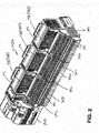
- FIG. 2 is an isometric view of a modular input/output (I/O) system MIO including at least one selectively installable and removable auxiliary wiring device XD in accordance with an embodiment of the present development. Except as otherwise shown and/or described herein, the modular I/O system MIO of FIG. 2 is similar to the modular I/O system MIO' of FIG. 1 , and like components of the modular I/O system MIO relative to the modular I/O system MIO' of FIG. 1 are identified with like reference characters that omit the primed (') designation, and in some cases such like components are not described in their entirety again here.
- I/O input/output
- the modular input/output (I/O) systems MIO includes a network adapter module AM and includes one or more terminal base units TB (TB1,TB2,TB3, etc.) operably connected to the adapter module AM.
- the adapter module AM is operatively connected to an industrial automation network N ( FIG. 1 ) so that the network adapter module AM receives data from, transmits data to, and otherwise communicates with an industrial control module or "controller" C also connected to the network N.
- a first terminal base unit TB1 is located adjacent and operably physically and electrically connected to the network adapter module AM and the additional terminal base units TB2,TB3 are operably physically and electrically connected together one after the other in a sequential manner such that a modular backplane circuit for communicating electrical power and data (referred to as a "backplane") is constructed through the successively connected terminal base units TB and operably connects each terminal base unit TB to the adapter module AM and, thus, to the associated industrial controller C to which the adapter module AM is operable connected.
- a backplane circuit for communicating electrical power and data referred to as a "backplane"
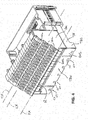
- each terminal base unit TB (sometimes referred to simply as a "terminal base”) includes a main body TBB and includes a terminal block BK that is connected to the main body TBB or that is defined as a part of the main body TBB.
- the terminal block BK comprises a plurality of cage clamps, spring clamps, screw terminals, or other wiring connectors WC that are adapted to be connected to field cables or field wires FW that are each associated with a field device FD that is typically an analog or digital device such as a sensor, switch, probe, thermocouple, RTD, encoder, or the like that is associated with the process or machine being controlled (the controlled system CS) by the controller C (see also FIG. 1 ).
- the wiring connectors WC are arranged in respective rows that each extend laterally along a connector axis CX that lies parallel to a longitudinal axis LX of the terminal block BK, and the longitudinal axis LX of the terminal block typically lies parallel to the DIN rail or other mounting structure to which the terminal base TB is operatively connected during use.
- the terminal base TB comprises a bottom wall TBW that partially defined by a bottom wall BW1 of the main body TBB and partially defined by a bottom wall W2 of the terminal block BK.
- a respective I/O module M (shown in FIG. 2 but not in FIGS. 3 & 4 ) is operatively removably connected to each terminal base TB such that the installed I/O module M communicates with the field device wiring connectors WC of the corresponding terminal base TB to which the I/O module M is physically connected, and the I/O module M also communicates with the network adapter module AM (and from there to the industrial automation controller C) over the backplane circuit such that input/output data is provided between the controller C and field device(s) FD connected to the corresponding terminal base TB.
- Each I/O module M is selected and configured to perform one or more specialized input/output functions such as DC input, DC output, AC input, AC output, analog input and/or output, RTD and/or thermocouple input and/or thermocouple output, or the like.
- a terminal block BK lacks the required number and/or type of wiring connectors WC necessary to complete the wiring for one or more associated field devices FD.
- the system MIO of FIG. 2 comprises at least one selectively installable and removable auxiliary wiring device XD that, when installed as shown in FIGS. 2 and 3 , is mechanically or physically engaged with and connected to a corresponding terminal base TB.
- the auxiliary wiring device XD comprises a plurality of auxiliary wiring connectors XC for being connected to one or more of the field wires FW and/or for being connected to an auxiliary input or output connection AX ( FIG.
- auxiliary wiring connectors XC are electrically connected in common with each other such that a connection of one of the auxiliary wiring connectors XC to the auxiliary input or output connection AX (e.g., an electrical ground path connection) connects all of the auxiliary wiring connectors XC to the auxiliary input or output connection.
- AX e.g., an electrical ground path connection
- at least one of the auxiliary wiring connectors XC is not electrically connected in common with the other auxiliary wiring connectors XC.
- the auxiliary wiring device XD is selectively removable from the terminal base TB when not needed or desired.
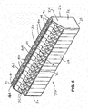
- FIGS. 5 and 6A - 6E show the selectively installable and removable auxiliary wiring device XD by itself.
- the auxiliary wiring device XD comprises a molded polymeric or otherwise constructed body 20 including the plurality of auxiliary wiring connectors XC. As noted above, one or more (or all) of the plurality of auxiliary wiring connectors can be electrically connected together to provide a common electrical connection point.
- the body includes a front wall 22, a rear wall 24, a top wall 26, a bottom wall 28, and opposite left and right lateral side walls 30,32.
- the top wall 26 is abutted with the bottom wall TBW of the terminal base TB.
- the auxiliary wiring connectors XC are located in the front wall 22 of the body 20.
- the body 20 can be constructed as one piece or, as shown herein, assembled from two or more pieces that are interconnected to define the body 20.
- each mounting tab 40 includes an inner face 42 oriented toward the auxiliary wiring connectors XC, and the inner face 42 is concave such that a mounting tab recess 40R is defined between each mounting tab 40 and the front wall 22. At least part of the inner face 42 preferably comprises a cylindrical surface 42c (See FIG.
- Each mounting tab 40 further comprises an outer face 44 located on the side opposite the inner face 42 and facing in the opposite direction as compared to the inner face 42.
- the outer face 44 of each mounting tab 40 is angled or otherwise transversely oriented with respect to the top wall 26.
- the body 20 of the auxiliary wiring device XD further comprises at least one and preferably at least two or more latch arms 50 that project outwardly from the body 20.
- the body includes a plurality of latch arms 50 spaced evenly across its width between the left and right side walls 30,32, with the latch arms projecting outwardly from the top wall 26 adjacent the intersection of the top wall 26 with the rear wall 24.
- each latch arm 50 comprises a resiliently flexible shaft or stem 52 that projects outwardly from the top wall 26, and includes an enlarged locking projection 54 connected to an outer end 52e of the stem 52 that is spaced from the top wall 26.
- the locking projection 54 comprises an inclined ramp face 54r that diverges away from the stem 52 as it extends from an outer end of the ramp face 54r located adjacent the outer end 52e of the stem 52 toward an inner end of the ramp face 54r that is located closer to the top wall 26 of the body 20 as compared to the outer end of the ramp face.
- the locking projection 54 further comprises a transverse lock face 54f that is oriented perpendicularly or otherwise transversely oriented relative to the stem 52 and that connects the inner end of the ramp face 54r to the stem 52 at a location between the top wall 26 of the body 20 and the outer end 52e of the stem 52.
- Each latch arm 50 is resiliently elastically deflectable at least toward and away from the front and back walls 22,24.
- the terminal block BK of the terminal base TB includes a receiver portion or receiver R adapted to receive the mounting tabs 40 of the body 20 of the auxiliary wiring device XD such that the auxiliary wiring device 20 is engaged with and pivotable relative to the terminal base TB when the mounting tabs 40 are received in and engaged with the receiver portion R.
- the receiver R is located adjacent the terminal base bottom wall TBW and, in the illustrated embodiment the receiver is connected to the terminal block BK and located adjacent the bottom wall BW2 of the terminal block BK.
- the receiver R comprises a recess or pocket RP that can comprise a single open space adapted to receive all of the mounting tabs 40 or can comprise a plurality of separate individual adjacent pocket spaces separated by divider walls, wherein each of individual pocket space is adapted to receive a respective one of the mounting tabs 40.
- the receiver comprises a projecting lip RL including a tip LT comprising a cylindrical surface centered on a receiver axis RX ( FIGS. 3 & 4 ) that extends parallel to longitudinal axis of the terminal block BK.
- the cylindrical surface of the tip LT is preferably formed with a radius that matches the radius of the cylindrical surface 42c of each mounting tab 40.As shown in FIGS.
- the auxiliary wiring device XD When the tip LT is located in the mounting tab recess 40R, the auxiliary wiring device XD is manually pivotable about the receiver axis RX relative to the terminal block BK such that the receiver axis RX defines or functions as a pivot axis for the auxiliary wiring device XD about which the auxiliary wiring device XD pivots relative to the terminal block BK portion of the terminal base TB.
- Each of the resilient latch arms 50 of the auxiliary wiring device XD is adapted to mate with and engage a respective catch CT of the terminal base TB.
- the terminal base TB comprises one or more such catches CT that correspond respectively to the resilient latch arms 50.
- the terminal base bottom wall TBW comprises a plurality of catches CT defined therein, wherein the catches CT of the illustrated embodiment are more particularly located in the bottom wall BW1 of the terminal base main body TBB.
- Each catch CT comprises a slot CS defined in the bottom wall TBW that is adapted to receive a respective latch arm 50.
- Each catch CT further comprises a transverse catch face CF ( FIGS. 7A - 7C ) that intersects the catch slot CS that is arranged transversely relative to the catch slot CS so that the catch face CF intersects the slot CS at an angle.
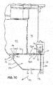
- FIGS. 7A - 7C Installation of the auxiliary wiring device XD to the terminal block portion BK of the terminal base TB is shown in FIGS. 7A - 7C .
- the auxiliary wiring device XD is located adjacent the terminal block BK and the mounting tabs 40 are aligned with the receiver R of the terminal base TB.
- the mounting tabs 40 are then inserted into the receiver pocket RP such that the tip LT of the projecting lip RL of the receiver R is received into the mounting tab recess 40R of the auxiliary wiring device and such that the tip LT is abutted with the concave inner face 42 of each mounting tab 40 to provide an installation position of the auxiliary wiring device XD.
- the auxiliary wiring device XD is then manually pivoted about the receiver (pivot) axis RX relative to the terminal block BK from the installation position ( FIG. 7B ) toward and into its operative position ( FIG. 7C ) such that the resilient latch arms 50 are each mated and engaged with a respective catch CT of the terminal base TB so that the auxiliary wiring device XD is fixedly secured to the terminal base TB in its operative position as shown in FIG. 7C .
- each resilient latch arm 50 contacts the catch CT, bottom wall TBW, and/or other part of the terminal base TB such that the resilient latch arm 50 is deflected sufficiently for its enlarged locking projection 54 to move into the catch slot CS and into alignment with the catch face CF.
- the latch arm 50 resiliently returns at least toward and optionally fully to its undeflected state and position such that the locking projection 54 is engaged with the catch face CF and so that the latch arm 50 is mated and engaged with the respective catch CT for fixed securement of the auxiliary wiring device XD to the terminal base TB adjacent with bottom wall TBW so that the auxiliary wiring device XD is located in its operative position.
- the latch arm 50 is mated with the catch CT
- the locking projection 54 of the latch arm 50 is abutted and frictionally engaged with the catch face CF.
- the auxiliary wiring connectors XC thereof extend laterally along an auxiliary connector axis UX that is parallel to the longitudinal axis LX and parallel to the receiver axis RX of the terminal block BK.
- the auxiliary wiring device XD is removed from the terminal base by reversing the above-noted installation steps, beginning with pivoting the auxiliary wiring device XD relative to the terminal base TB in a second (removal) direction A2 that is opposite the first (installation) direction A1 as shown in FIG. 7C .
- the catch face CF is preferably oriented such that the enlarged locking projection 54 of the respective latch arm 50 is frictionally engaged with the catch face CF when the latch arm 50 is mated with the catch CT, but also such that when the auxiliary wiring device XD is pivoted in the second direction A2, the catch face CF deflects the latch arm 50 away from the catch face CF to allow the latch arm 50 to disengage from the catch CT.
- Each latch arm 50 resiliently resumes its undeflected free state after it is disengaged from its respective catch CT.
- the body 20 of the auxiliary wiring device XD optionally includes a tool recess TR adapted to receive the blade of a tool such as a screwdriver that is used to pivot the auxiliary wiring device XD in the second direction A2 relative to the terminal base TB.
- the tool recess TR can be integrally formed as part of the body 20.
- the auxiliary wiring device XD comprises a backing plate BP connected to the body 20 adjacent the rear wall 24 of the body, and the tool recess TR is provided or defined as part of the backing plate BP.
- the auxiliary wiring device XD When operatively installed, the auxiliary wiring device XD provides a convenient location for auxiliary wiring connections for the field wires FW or other connections in a manner where the auxiliary wiring connectors XC are located adjacent the main wiring connectors of the terminal block BK. As noted, in one embodiment, all or some of the auxiliary wiring connectors XC are electrically connected together such that each auxiliary wiring connector XC is electrically common with the other auxiliary wiring connectors XC, or two or more of the auxiliary wiring connectors XC are alternatively electrically isolated from the other auxiliary wiring connectors XC.
Landscapes
- Engineering & Computer Science (AREA)
- Microelectronics & Electronic Packaging (AREA)
- Automation & Control Theory (AREA)
- Connections Arranged To Contact A Plurality Of Conductors (AREA)
- Connector Housings Or Holding Contact Members (AREA)
Description
- Modular input/output (I/O) systems for industrial automation control systems are well-known and in widespread use. Referring to
FIG. 1 , a known modular I/O system MIO' includes a network adapter module AM' that is operatively connected to an industrial automation network N so that the network adapter module AM' receives data from, transmits data to, and otherwise communicates with an industrial control module or "controller" C also connected to the network N. - The adapter module AM' is mounted to a DIN rail D or other support structure. One or more terminal base units TB' (TB1',TB2',TB3', etc.) are also mounted to the DIN rail D, with a first terminal base unit TBI' located adjacent and operably physically and electrically connected to the network adapter module AM' and with the additional terminal base units TB2',TB3' operably physically and electrically connected together one after the other in a sequential manner such that a modular backplane circuit for communicating electrical power and data (referred to as a "backplane") is constructed through the successively connected terminal base units TB' and operably connects each terminal base unit TB' to the adapter module AM' and, thus, to the controller C.
- Each terminal base unit TB' (sometimes referred to simply as a "terminal base") includes a terminal block BK' comprising a plurality of cage clamps, spring clamps, screw terminals, or other wiring connectors WC' that are adapted to be connected to field cables or field wires FW that are each associated with a field device FD that is typically an analog or digital device such as a sensor, switch, probe, thermocouple, RTD, encoder, or the like that is associated with the process or machine being controlled (the controlled system CS) by the controller C. The terminal block BK' is typically a separate structure that is assembled to the terminal base TB' but the terminal block BK' can alternatively be defined as an integral or one-piece part of the terminal base TB'. Different varieties of terminal blocks BX' can be used depending upon the particular configuration required for the field device wiring connectors WC', with some having different common terminals, ground connections, voltage supply terminals, and the like.
- A respective I/O module M' is operatively removably connected to each terminal base TB' such that the installed I/O module M' communicates with the field device wiring connectors WC' of the corresponding terminal base TB' to which the I/O module M' is physically connected, and the I/O module M' also communicates with the network adapter module AM' (and from there to the industrial automation controller C) over the backplane circuit such that input/output data is provided between the controller C and field device(s) FD connected to the corresponding terminal base TB'. Each I/O module M' is selected and configured to perform one or more specialized input/output functions such as DC input, DC output, AC input, AC output, analog input and/or output, RTD and/or thermocouple input and/or thermocouple output, or the like.
- In certain instances, a terminal block BK' lacks the required number and/or type of wiring connectors WC' necessary to complete the wiring for one or more associated field devices FD. In such case, using presently known systems, it is necessary for an end user to install a separate auxiliary wiring connector device XD' as near as possible to the relevant terminal base TB'. In this known arrangement, the auxiliary wiring connector device XD' is separate and spaced-apart from the terminal block BK' and is provided with the necessary power, ground, or other auxiliary wiring connections XC'. One or more of the auxiliary wiring connectors XC' is connected to an auxiliary input or output connection AX such as a ground path, a voltage supply, a conditioning circuit, or the like. The field device wiring or related cabling/wiring must be lengthened and/or otherwise routed to mate with the wiring connections XC' of the separate auxiliary wiring device XD' (see field wires FW') which makes the wiring system more complicated and less efficient. Also, the use of such a separate auxiliary wiring connector device XD' makes it more difficult for maintenance and service personnel to understand the original wiring pattern and to duplicate same as needed after removal and replacement of a defective terminal base TB'. Accordingly, a need has been identified for an auxiliary wiring device that overcomes these and other deficiencies while providing better overall results.
-
US 2014/0194007 A1 relates to a control apparatus comprising a module having first and second module parts, which can be mechanically and electrically combined to form a combined arrangement. The first and second module parts each comprise a housing having a boundary surface opposite one another in the combined arrangement that define a boundary plane. The first and second module parts are combined by a pivoting movement about a pivot axis arranged perpendicular to the boundary plane. One of the module parts has a number of contacts comprising a first electrical contact, and the other module part has a number of mating contacts comprising a first electrical mating contact. In the combined arrangement, each electrical contact makes contact with its corresponding mating contact for electrical connection between the first and second module parts. The contacts comprise conductor tracks on a nonconductive board such that a printed circuit board is formed. -
US 2010/240237 A1 relates to an electrical additional module, having an appliance interface for fitting the additional module to a service device, with the service device having a stepped holding geometry with at least two steps on each of which a contact device is arranged for holding an electrical opposing contact device, with the appliance interface having step sections which are designed to be complementary to the at least two steps and on which in each case one of the electrical opposing contact device is arranged in order to make contact with the associated contact device, and with the at least two step sections being rigidly connected to one another when the additional module is not fitted. - It is the object of the present invention to provide an improved modular I/O device.
- The object is solved by the subject matter of the independent claim.
- Preferred embodiments of the present invention are defined by the dependent claims. Described embodiments that do not fall within the scope of the claims, are not part of the invention.
- In accordance with one aspect of the present development, a modular I/O device includes a terminal base including a terminal block. The terminal block includes a plurality of wiring connectors adapted for connection to associated field device wires. An auxiliary wiring device includes a plurality of auxiliary wiring connectors adapted for connection to associated field device wires. The auxiliary wiring device is selectively physically connectable to said terminal base in an operative position and selectively physically removable from said terminal base.
- In accordance with another aspect of the present development, the terminal block includes a receiver and the auxiliary wiring device includes a body including at least one mounting tab that projects outwardly from the body, wherein the at least one mounting tab is located in the receiver when the auxiliary wiring device is connected to the terminal base.
- In accordance with a further aspect of the present development, the receiver comprises an open pocket into which the at least one mounting tab is inserted. The receiver includes a projecting lip with a tip that is abutted with an inner face of the at least one mounting tab. The tip of the projecting lip of the receiver and the inner face of the at least one mounting tab comprise respective cylindrical surfaces that are abutted with each other when the auxiliary wiring device is connected to the terminal base such that the abutted cylindrical surfaces provide a pivoting hinge interface about which the auxiliary wiring device is pivotable relative to the receiver on a pivot axis.
- In accordance with another aspect of the present development, the terminal base includes at least one catch, and wherein the body of said auxiliary wiring device further includes at least one latch arm connected thereto that is adapted to mate with and engage the at least one catch when the auxiliary wiring device is physically connected to said terminal base in its operative position.
- In accordance with a further aspect of the present development, the at least one latch arm comprises a resiliently flexible latch arm including a locking projection that is adapted to engage the at least one catch when the at least one latch arm is mated with the at least one catch. The at least one catch comprises: (i) a slot located in a bottom wall of the terminal base that is adapted to receive the at least one latch arm. The catch includes a transverse catch face that intersects the slot. The at least one latch arm is received in the slot and the locking projection thereof engages the transverse catch face when the at least one latch arm is mated with the at least one catch.
- In one embodiment, the at least one latch arm includes a resiliently flexible stem that projects outwardly from the body, and the locking projection is located at an outer end of the stem spaced from the body. The locking projection includes: (i) an inclined ramp face that diverges away from the stem as the inclined ramp face extends from the outer end of the stem toward the body; and, (ii) a transverse lock face that connects an inner end of the inclined ramp face to the stem.
- In accordance with another aspect of the present development, at least some of the auxiliary wiring connectors of the auxiliary wiring device are electrically interconnected in common with each other.
- In accordance with a further aspect of the present development, the body of the auxiliary wiring device also includes a tool recess that is adapted to receive an associated tool used to pivot the auxiliary wiring device about the pivot axis from the operative position toward the installation position.
-
-
FIG. 1 (prior art) is a front view of a known modular input/output (I/O) system; -
FIG. 2 is an isometric view of a modular input/output (I/O) system provided in accordance with an embodiment of the present development to include at least one selectively installable and removable auxiliary wiring device; -
FIG. 3 is an isometric view of a single terminal base of the I/O system ofFIG. 2 (without including its associated I/O module connected thereto) including a selectively installable and removable auxiliary wiring device according to the present development; -
FIG. 4 is similar toFIG. 3 but shows the terminal base without the auxiliary wiring device installed; -
FIG. 5 is a front isometric view of the selectively installable and removable auxiliary wiring device by itself; -
FIGS. 6A, 6B, 6C, 6D, and 6E are respective front, top, bottom, left side, and right side views of the auxiliary wiring device shown inFIG. 5 ; -
FIGS. 7A ,7B , and7C are simplified side section views that respectively illustrate first, second, and third steps of a process for selectively installing the auxiliary wiring device ofFIG. 5 on a terminal base according to the present development (the process for removing the auxiliary wiring device from the terminal base comprises performing the first, second, and third steps in the reverse order). -
FIG. 2 is an isometric view of a modular input/output (I/O) system MIO including at least one selectively installable and removable auxiliary wiring device XD in accordance with an embodiment of the present development. Except as otherwise shown and/or described herein, the modular I/O system MIO ofFIG. 2 is similar to the modular I/O system MIO' ofFIG. 1 , and like components of the modular I/O system MIO relative to the modular I/O system MIO' ofFIG. 1 are identified with like reference characters that omit the primed (') designation, and in some cases such like components are not described in their entirety again here. - The modular input/output (I/O) systems MIO includes a network adapter module AM and includes one or more terminal base units TB (TB1,TB2,TB3, etc.) operably connected to the adapter module AM. The adapter module AM is operatively connected to an industrial automation network N (
FIG. 1 ) so that the network adapter module AM receives data from, transmits data to, and otherwise communicates with an industrial control module or "controller" C also connected to the network N. A first terminal base unit TB1 is located adjacent and operably physically and electrically connected to the network adapter module AM and the additional terminal base units TB2,TB3 are operably physically and electrically connected together one after the other in a sequential manner such that a modular backplane circuit for communicating electrical power and data (referred to as a "backplane") is constructed through the successively connected terminal base units TB and operably connects each terminal base unit TB to the adapter module AM and, thus, to the associated industrial controller C to which the adapter module AM is operable connected. - Referring also to
FIGS. 3 &4 , each terminal base unit TB (sometimes referred to simply as a "terminal base") includes a main body TBB and includes a terminal block BK that is connected to the main body TBB or that is defined as a part of the main body TBB. The terminal block BK comprises a plurality of cage clamps, spring clamps, screw terminals, or other wiring connectors WC that are adapted to be connected to field cables or field wires FW that are each associated with a field device FD that is typically an analog or digital device such as a sensor, switch, probe, thermocouple, RTD, encoder, or the like that is associated with the process or machine being controlled (the controlled system CS) by the controller C (see alsoFIG. 1 ). The wiring connectors WC are arranged in respective rows that each extend laterally along a connector axis CX that lies parallel to a longitudinal axis LX of the terminal block BK, and the longitudinal axis LX of the terminal block typically lies parallel to the DIN rail or other mounting structure to which the terminal base TB is operatively connected during use. As shown inFIG. 4 , the terminal base TB comprises a bottom wall TBW that partially defined by a bottom wall BW1 of the main body TBB and partially defined by a bottom wall W2 of the terminal block BK. - A respective I/O module M (shown in
FIG. 2 but not inFIGS. 3 &4 ) is operatively removably connected to each terminal base TB such that the installed I/O module M communicates with the field device wiring connectors WC of the corresponding terminal base TB to which the I/O module M is physically connected, and the I/O module M also communicates with the network adapter module AM (and from there to the industrial automation controller C) over the backplane circuit such that input/output data is provided between the controller C and field device(s) FD connected to the corresponding terminal base TB. Each I/O module M is selected and configured to perform one or more specialized input/output functions such as DC input, DC output, AC input, AC output, analog input and/or output, RTD and/or thermocouple input and/or thermocouple output, or the like. - As noted above, in certain instances, a terminal block BK lacks the required number and/or type of wiring connectors WC necessary to complete the wiring for one or more associated field devices FD. Unlike the known modular I/O system MIO' of
FIG. 1 , the system MIO ofFIG. 2 comprises at least one selectively installable and removable auxiliary wiring device XD that, when installed as shown inFIGS. 2 and3 , is mechanically or physically engaged with and connected to a corresponding terminal base TB. The auxiliary wiring device XD comprises a plurality of auxiliary wiring connectors XC for being connected to one or more of the field wires FW and/or for being connected to an auxiliary input or output connection AX (FIG. 1 ) such as a ground path, a voltage supply, a conditioning circuit, or the like. In one embodiment, all of the auxiliary wiring connectors XC are electrically connected in common with each other such that a connection of one of the auxiliary wiring connectors XC to the auxiliary input or output connection AX (e.g., an electrical ground path connection) connects all of the auxiliary wiring connectors XC to the auxiliary input or output connection. In an alternative embodiment, at least one of the auxiliary wiring connectors XC is not electrically connected in common with the other auxiliary wiring connectors XC. As shown inFIG. 4 , the auxiliary wiring device XD is selectively removable from the terminal base TB when not needed or desired. -
FIGS. 5 and6A - 6E show the selectively installable and removable auxiliary wiring device XD by itself. The auxiliary wiring device XD comprises a molded polymeric or otherwise constructedbody 20 including the plurality of auxiliary wiring connectors XC. As noted above, one or more (or all) of the plurality of auxiliary wiring connectors can be electrically connected together to provide a common electrical connection point. The body includes afront wall 22, arear wall 24, atop wall 26, abottom wall 28, and opposite left and rightlateral side walls FIG. 3 , thetop wall 26 is abutted with the bottom wall TBW of the terminal base TB. The auxiliary wiring connectors XC are located in thefront wall 22 of thebody 20. Thebody 20 can be constructed as one piece or, as shown herein, assembled from two or more pieces that are interconnected to define thebody 20. - Adjacent the intersection of the
front wall 22 and thetop wall 26, thebody 20 comprises at least one and preferably at least two mountingtabs 40 that project outwardly from thefront wall 22. In the illustrated embodiment, a plurality of mountingtabs 40 are provided and are evenly spaced across the width of thebody 20 between the left andright side walls front wall 22 andtop wall 26. With reference also to the enlarged views ofFIGS. 7A - 7C , each mountingtab 40 includes aninner face 42 oriented toward the auxiliary wiring connectors XC, and theinner face 42 is concave such that a mountingtab recess 40R is defined between each mountingtab 40 and thefront wall 22. At least part of theinner face 42 preferably comprises acylindrical surface 42c (SeeFIG. 7A ). Each mountingtab 40 further comprises anouter face 44 located on the side opposite theinner face 42 and facing in the opposite direction as compared to theinner face 42. Theouter face 44 of each mountingtab 40 is angled or otherwise transversely oriented with respect to thetop wall 26. - The
body 20 of the auxiliary wiring device XD further comprises at least one and preferably at least two ormore latch arms 50 that project outwardly from thebody 20. In the example of the illustrated embodiment, the body includes a plurality oflatch arms 50 spaced evenly across its width between the left andright side walls top wall 26 adjacent the intersection of thetop wall 26 with therear wall 24. Referring also to the enlarged views ofFIGS. 7A - 7C , eachlatch arm 50 comprises a resiliently flexible shaft or stem 52 that projects outwardly from thetop wall 26, and includes anenlarged locking projection 54 connected to anouter end 52e of thestem 52 that is spaced from thetop wall 26. As shown herein, the lockingprojection 54 comprises aninclined ramp face 54r that diverges away from thestem 52 as it extends from an outer end of theramp face 54r located adjacent theouter end 52e of thestem 52 toward an inner end of theramp face 54r that is located closer to thetop wall 26 of thebody 20 as compared to the outer end of the ramp face. The lockingprojection 54 further comprises atransverse lock face 54f that is oriented perpendicularly or otherwise transversely oriented relative to thestem 52 and that connects the inner end of theramp face 54r to thestem 52 at a location between thetop wall 26 of thebody 20 and theouter end 52e of thestem 52. Eachlatch arm 50 is resiliently elastically deflectable at least toward and away from the front andback walls - Referring to
FIGS. 3 ,4 and7A - 7C , the terminal block BK of the terminal base TB includes a receiver portion or receiver R adapted to receive the mountingtabs 40 of thebody 20 of the auxiliary wiring device XD such that theauxiliary wiring device 20 is engaged with and pivotable relative to the terminal base TB when the mountingtabs 40 are received in and engaged with the receiver portion R. The receiver R is located adjacent the terminal base bottom wall TBW and, in the illustrated embodiment the receiver is connected to the terminal block BK and located adjacent the bottom wall BW2 of the terminal block BK. More particularly, the receiver R comprises a recess or pocket RP that can comprise a single open space adapted to receive all of the mountingtabs 40 or can comprise a plurality of separate individual adjacent pocket spaces separated by divider walls, wherein each of individual pocket space is adapted to receive a respective one of the mountingtabs 40. In either case, the receiver comprises a projecting lip RL including a tip LT comprising a cylindrical surface centered on a receiver axis RX (FIGS. 3 &4 ) that extends parallel to longitudinal axis of the terminal block BK. The cylindrical surface of the tip LT is preferably formed with a radius that matches the radius of thecylindrical surface 42c of each mounting tab 40.As shown inFIGS. 7A &7B , when a mountingtab 40 of theauxiliary wiring device 20 is inserted into the receiver pocket RP, the tip LT is received in the mountingtab recess 40R and the cylindrical surface of the tip LT is abutted with the mutually correspondingcylindrical portion 42c of the concaveinner face 42 of each mountingtab 40 to provide a pivoting hinge interface between each mountingtab 40 and the projecting lip RL of the receiver pocket. When the tip LT is located in the mountingtab recess 40R, the auxiliary wiring device XD is manually pivotable about the receiver axis RX relative to the terminal block BK such that the receiver axis RX defines or functions as a pivot axis for the auxiliary wiring device XD about which the auxiliary wiring device XD pivots relative to the terminal block BK portion of the terminal base TB. - Each of the
resilient latch arms 50 of the auxiliary wiring device XD is adapted to mate with and engage a respective catch CT of the terminal base TB. In particular, the terminal base TB comprises one or more such catches CT that correspond respectively to theresilient latch arms 50. In the illustrated embodiment, the terminal base bottom wall TBW comprises a plurality of catches CT defined therein, wherein the catches CT of the illustrated embodiment are more particularly located in the bottom wall BW1 of the terminal base main body TBB. Each catch CT comprises a slot CS defined in the bottom wall TBW that is adapted to receive arespective latch arm 50. Each catch CT further comprises a transverse catch face CF (FIGS. 7A - 7C ) that intersects the catch slot CS that is arranged transversely relative to the catch slot CS so that the catch face CF intersects the slot CS at an angle. - Installation of the auxiliary wiring device XD to the terminal block portion BK of the terminal base TB is shown in
FIGS. 7A - 7C . In an initial step shown inFIG. 7A , the auxiliary wiring device XD is located adjacent the terminal block BK and the mountingtabs 40 are aligned with the receiver R of the terminal base TB. As shown inFIG. 7B , the mountingtabs 40 are then inserted into the receiver pocket RP such that the tip LT of the projecting lip RL of the receiver R is received into the mountingtab recess 40R of the auxiliary wiring device and such that the tip LT is abutted with the concaveinner face 42 of each mountingtab 40 to provide an installation position of the auxiliary wiring device XD. - As indicated by the arrow A1 in
FIG. 7B , the auxiliary wiring device XD is then manually pivoted about the receiver (pivot) axis RX relative to the terminal block BK from the installation position (FIG. 7B ) toward and into its operative position (FIG. 7C ) such that theresilient latch arms 50 are each mated and engaged with a respective catch CT of the terminal base TB so that the auxiliary wiring device XD is fixedly secured to the terminal base TB in its operative position as shown inFIG. 7C . More specifically, when the auxiliary wiring device XD is pivoted toward its operative position in a first or installation direction as indicated by the arrow A1, theramp face 54r of eachresilient latch arm 50 contacts the catch CT, bottom wall TBW, and/or other part of the terminal base TB such that theresilient latch arm 50 is deflected sufficiently for itsenlarged locking projection 54 to move into the catch slot CS and into alignment with the catch face CF. When the lockingprojection 54 is aligned with thecatch face 54, thelatch arm 50 resiliently returns at least toward and optionally fully to its undeflected state and position such that the lockingprojection 54 is engaged with the catch face CF and so that thelatch arm 50 is mated and engaged with the respective catch CT for fixed securement of the auxiliary wiring device XD to the terminal base TB adjacent with bottom wall TBW so that the auxiliary wiring device XD is located in its operative position. When thelatch arm 50 is mated with the catch CT, the lockingprojection 54 of thelatch arm 50 is abutted and frictionally engaged with the catch face CF. When the auxiliary wiring device XD is operatively installed on the terminal base TB as shown inFIGS. 3 and7C , the auxiliary wiring connectors XC thereof extend laterally along an auxiliary connector axis UX that is parallel to the longitudinal axis LX and parallel to the receiver axis RX of the terminal block BK. - The auxiliary wiring device XD is removed from the terminal base by reversing the above-noted installation steps, beginning with pivoting the auxiliary wiring device XD relative to the terminal base TB in a second (removal) direction A2 that is opposite the first (installation) direction A1 as shown in
FIG. 7C . The catch face CF is preferably oriented such that theenlarged locking projection 54 of therespective latch arm 50 is frictionally engaged with the catch face CF when thelatch arm 50 is mated with the catch CT, but also such that when the auxiliary wiring device XD is pivoted in the second direction A2, the catch face CF deflects thelatch arm 50 away from the catch face CF to allow thelatch arm 50 to disengage from the catch CT. Eachlatch arm 50 resiliently resumes its undeflected free state after it is disengaged from its respective catch CT. - To assist in removing the auxiliary wiring device XD from the terminal base TB, the
body 20 of the auxiliary wiring device XD optionally includes a tool recess TR adapted to receive the blade of a tool such as a screwdriver that is used to pivot the auxiliary wiring device XD in the second direction A2 relative to the terminal base TB. The tool recess TR can be integrally formed as part of thebody 20. In the illustrated embodiment, the auxiliary wiring device XD comprises a backing plate BP connected to thebody 20 adjacent therear wall 24 of the body, and the tool recess TR is provided or defined as part of the backing plate BP. - When operatively installed, the auxiliary wiring device XD provides a convenient location for auxiliary wiring connections for the field wires FW or other connections in a manner where the auxiliary wiring connectors XC are located adjacent the main wiring connectors of the terminal block BK. As noted, in one embodiment, all or some of the auxiliary wiring connectors XC are electrically connected together such that each auxiliary wiring connector XC is electrically common with the other auxiliary wiring connectors XC, or two or more of the auxiliary wiring connectors XC are alternatively electrically isolated from the other auxiliary wiring connectors XC.
- In the preceding specification, various embodiments have been described with reference to the accompanying drawings. It will, however, be evident that various modifications and changes may be made thereto, and additional embodiments may be implemented, without departing from the broader scope of the invention as set forth in the claims that follow. The specification and drawings are accordingly to be regarded in an illustrative rather than restrictive sense.
Claims (15)
- A modular I/O device comprising:a terminal base (TB) including a terminal block, said terminal block comprising a plurality of wiring connectors adapted for connection to associated field device wires;an auxiliary wiring device (XD) comprising a plurality of auxiliary wiring connectors adapted for connection to associated field device wires, said auxiliary wiring device (XD) selectively physically connectable to said terminal base in an operative position and selectively physically removable from said terminal base;characterized in thatsaid terminal block (TB) comprises a receiver (R) and said auxiliary wiring device (XD) comprises a body (20) including at least one mounting tab (40) that projects outwardly from the body (20), wherein said at least one mounting tab (40) is located in said receiver (R) when said auxiliary wiring device (XD) is connected to said terminal base (TB),said receiver (R) comprises an open pocket (RP) into which said at least one mounting tab (40) is inserted when said auxiliary wiring device (XD) is connected to said terminal base (TB), andsaid terminal base (TB) comprises at least one catch (CT), and wherein said body (20) of said auxiliary wiring device (XD) further comprises at least one latch arm (50) connected thereto that is adapted to mate with and engage said at least one catch (CT) when said auxiliary wiring device (XD) is physically connected to said terminal base (TB) in said operative position.
- The modular I/O device as set forth in claim 1, wherein said at least one mounting tab (40) of said auxiliary wiring device (XD) comprises at least two mounting tabs (40).
- The modular I/O device as set forth in claim 1, wherein said receiver (R) comprises a projecting lip (RL) that extends along a receiver axis, wherein said projecting lip (RL) comprises a tip (LT) that is abutted with an inner face of said at least one mounting tab (40) when said auxiliary wiring device (XD) is connected to said terminal base (TB).
- The modular I/O device as set forth in claim 3, wherein said tip (LT) of said projecting lip (RL) of said receiver (R) and said inner face of said at least one mounting tab (40) comprise respective cylindrical surfaces that are abutted with each other when the auxiliary wiring device (XD) is connected to said terminal base (TB) such that said abutted cylindrical surfaces provide a pivoting hinge interface such that said auxiliary wiring device (XD) is pivotable relative to said receiver (R) about a pivot axis.
- The modular I/O device as set forth in claim 4, wherein:said terminal block comprises a longitudinal axis and said wiring connectors of said terminal block extend along a wiring connector axis that extends parallel to the longitudinal axis of said terminal block; and,said pivot axis lies parallel to said longitudinal axis of said terminal block; and/orwherein said terminal base (TB) is adapted to be connected to an associated DIN rail that extends parallel to the longitudinal axis of said terminal block.
- The modular I/O device as set forth in claim 1, wherein said at least one latch arm (50) comprises a resiliently flexible latch arm including a locking projection (54) that is adapted to engage said at least one catch (CT) when said at least one latch arm (50) is mated with said at least one catch (CT).
- The modular I/O device as set forth in claim 6, wherein said at least one catch (CT) comprises: (i) a slot (CS) located in a bottom wall (TBW) of said terminal base (TB) and adapted to receive said at least one latch arm (50); and, (ii) a transverse catch face (CF) that intersects said slot (CS).
- The modular I/O device as set forth in claim 7, wherein said at least one latch arm (50) is received in said slot (CS) and said locking projection (54) engages said transverse catch face (CF) when said at least one latch arm (50) is mated with said at least one catch (CT).
- The modular I/O device as set forth in claim 8, wherein said at least one latch arm (50) comprises a resiliently flexible stem (52) that projects outwardly from said body (20), and wherein said locking projection (54) is located at an outer end of the stem (52) spaced from the body (20), said locking projection (54) comprising: (i) an inclined ramp face (54r) that diverges away from the stem (52) as the inclined ramp face (54r) extends from the outer end of the stem (52) toward the body (20); and, (ii) a transverse lock face (54f) that connects an inner end of the inclined ramp face (54r) to the stem (52).
- The modular I/O device as set forth in claim 9, wherein said at least one latch arm (50) deflects relative to said body (20) of said auxiliary wiring device (XD) when said auxiliary wiring (XD) device is pivoted about said pivot axis from an installation position toward said operative position when said inclined ramp face (54r) contacts said terminal base (TB).
- The modular I/O device as set forth in claim 10, wherein said at least one latch arm (50) resiliently deflects relative to and disengages from said catch face (CF) in response to pivoting movement of said auxiliary wiring device (XD) about said pivot axis from said operative position toward said install position.
- The modular I/O device as set forth in claim 11, wherein said at least one latch arm (50) comprises at least two latch arms (50) and said at least one catch (CT) comprises at least two catches (CT) respectively corresponding to said at least two latch arms (50).
- The modular I/O device as set forth in claim 11, wherein at least some of said auxiliary wiring connectors of said auxiliary wiring device (XD) are electrically interconnected in common with each other.
- The modular I/O device as set forth in claim 13, wherein all of said auxiliary wiring connectors of said auxiliary wiring device (XD) are electrically interconnected in common with each other.
- The modular I/O device as set forth in claim 13, wherein said body (20) further comprises a tool recess (TR) that is adapted to receive an associated tool used to pivot said auxiliary wiring device (XD) about said pivot axis from said operative position toward said installation position; and
wherein said auxiliary wiring device (XD) comprises a backing plate (BP) connected to said body (20) and wherein said tool recess (TR) is defined as part of the backing plate (BP).
Applications Claiming Priority (1)
| Application Number | Priority Date | Filing Date | Title |
|---|---|---|---|
| US15/810,025 US10194553B1 (en) | 2017-11-11 | 2017-11-11 | Selectively installable and removable auxiliary wiring device for I/O module |
Publications (2)
| Publication Number | Publication Date |
|---|---|
| EP3484253A1 EP3484253A1 (en) | 2019-05-15 |
| EP3484253B1 true EP3484253B1 (en) | 2020-12-30 |
Family
ID=64331619
Family Applications (1)
| Application Number | Title | Priority Date | Filing Date |
|---|---|---|---|
| EP18204672.2A Active EP3484253B1 (en) | 2017-11-11 | 2018-11-06 | Selectively installable and removable auxiliary wiring device for i/o module |
Country Status (2)
| Country | Link |
|---|---|
| US (2) | US10194553B1 (en) |
| EP (1) | EP3484253B1 (en) |
Families Citing this family (9)
| Publication number | Priority date | Publication date | Assignee | Title |
|---|---|---|---|---|
| USD925454S1 (en) * | 2017-11-11 | 2021-07-20 | Rockwell Automation Asia Pacific Business Center Pte. Ltd. | Auxiliary wiring device for an I/O module |
| JP1605429S (en) * | 2017-11-24 | 2019-05-27 | ||
| JP1605962S (en) * | 2017-11-24 | 2019-05-27 | ||
| JP1605963S (en) * | 2017-11-24 | 2019-05-27 | ||
| JP1605430S (en) * | 2017-11-24 | 2019-05-27 | ||
| US11412632B2 (en) | 2019-06-11 | 2022-08-09 | Rockwell Automation Asia Pacific Business Center Pte. Ltd. | Isolated power smart terminal block |
| US10986748B1 (en) * | 2019-09-26 | 2021-04-20 | Rockwell Automation Technologies, Inc. | Input/output system |
| DE102020106085A1 (en) * | 2020-03-06 | 2021-09-09 | Phoenix Contact Gmbh & Co. Kg | Connection device and electromechanical assembly |
| EP4114156B1 (en) * | 2021-06-29 | 2025-08-06 | Abb Schweiz Ag | A terminal block unit for an input/output device of a modular process control system |
Family Cites Families (21)
| Publication number | Priority date | Publication date | Assignee | Title |
|---|---|---|---|---|
| US5253140A (en) * | 1988-03-12 | 1993-10-12 | Fanuc Ltd. | Connector unit for input/output module of programmable controller having disengagement lever |
| US4872855A (en) * | 1988-06-03 | 1989-10-10 | Connectron, Inc. | Adjustable terminal block equipment |
| US5148353A (en) * | 1990-06-29 | 1992-09-15 | Digital Equipment Corporation | Mounting system for installation of communication boxes having a convex bottom post and a rigid top post |
| US5302136A (en) * | 1992-11-23 | 1994-04-12 | Modicon, Inc. | Apparatus for positively preventing misengagement of multipoint connector elements |
| DE4438804C1 (en) * | 1994-10-31 | 1996-03-28 | Weidmueller Interface | Modular control system with bus conductor e.g. B. for building automation |
| DE19650989C2 (en) | 1996-11-28 | 2003-06-26 | Wago Verwaltungs Gmbh | Terminal block with side bridging contacts |
| US6033268A (en) * | 1997-04-30 | 2000-03-07 | Westinghouse Electric Corporation | Modular I/O system with two-way connectors between units and a common lock for multiple plug-in modules |
| US6654255B2 (en) * | 1999-12-02 | 2003-11-25 | Adtran, Inc. | System for mounting data communication equipment |
| DE102006003064B4 (en) * | 2006-01-20 | 2010-04-15 | Phoenix Contact Gmbh & Co. Kg | Electrical terminal block |
| EP2059976A1 (en) * | 2006-09-08 | 2009-05-20 | Siemens Aktiengesellschaft | Electrical additional module for a service device, combination of the additional module with the service device, as well as an additional module set |
| US7663867B2 (en) * | 2008-04-15 | 2010-02-16 | General Electric Company | Secondary circuit terminal block design for fixed type circuit breakers |
| US8986033B2 (en) * | 2010-03-31 | 2015-03-24 | Weidmueller Interface Gmbh & Co. Kg | Connection module being capable of serving as a bus |
| US9055687B2 (en) | 2010-08-20 | 2015-06-09 | Rockwell Automation Technologies, Inc. | Input/output circuits and devices having physically corresponding status indicators |
| DE102011110184A1 (en) * | 2011-08-09 | 2013-02-14 | Pilz Gmbh & Co. Kg | Modular control device |
| US9003095B2 (en) * | 2012-03-20 | 2015-04-07 | Rockwell Automation Technologies, Inc. | Automation control component |
| JP5614662B2 (en) * | 2012-10-26 | 2014-10-29 | 横河電機株式会社 | Input/Output Modules |
| US9325110B2 (en) | 2014-02-27 | 2016-04-26 | Rockwell Automation Technologies, Inc. | Input/output module |
| USD792857S1 (en) | 2015-03-23 | 2017-07-25 | Rockwell Automation Technologies, Inc. | Removable terminal block |
| US10162783B2 (en) * | 2015-03-27 | 2018-12-25 | Rockwell Automation Technologies, Inc. | Method and system for defining slot addresses |
| US9864352B2 (en) * | 2015-06-01 | 2018-01-09 | Rockwell Automation Asia Pacific Business Ctr. Pte., Ltd. | Slice I/O—field power bus breaker |
| US9966714B1 (en) * | 2017-07-05 | 2018-05-08 | Rockwell Automation Asia Pacific Business Ctr. Pte., Ltd. | I/O migration adapter for control system |
-
2017
- 2017-11-11 US US15/810,025 patent/US10194553B1/en active Active
-
2018
- 2018-11-06 EP EP18204672.2A patent/EP3484253B1/en active Active
-
2019
- 2019-01-28 US US16/259,627 patent/US10667422B2/en active Active
Non-Patent Citations (1)
| Title |
|---|
| None * |
Also Published As
| Publication number | Publication date |
|---|---|
| US10667422B2 (en) | 2020-05-26 |
| EP3484253A1 (en) | 2019-05-15 |
| US10194553B1 (en) | 2019-01-29 |
| US20190159357A1 (en) | 2019-05-23 |
Similar Documents
| Publication | Publication Date | Title |
|---|---|---|
| EP3484253A1 (en) | Selectively installable and removable auxiliary wiring device for i/o module | |
| EP2421347B1 (en) | Input/output module bus contact system and method | |
| CN103858281B (en) | Modular control system | |
| CN104488370B (en) | connection system | |
| EP2824767B1 (en) | Busbar connection system for use with a power distribution system, and Electrical device including the bubar connection system | |
| CN103858531B (en) | Modular control device | |
| CN105006717B (en) | Busbar connector system | |
| US10368458B2 (en) | Rail-mounted control system with improved mounting | |
| US9727098B2 (en) | Redundant power supply motherboard assembly | |
| CN104854972B (en) | For controlling and/or regulating the device of technical equipment | |
| US5668698A (en) | Smart connector for an electrical device | |
| CN103858062B (en) | Modular control equipment | |
| JP2000148214A (en) | Programmable logic controller and programmable logic controller module | |
| EP2506692A2 (en) | Din rail mountable base for process fieldbus redundant power conditioner | |
| EP3751972B1 (en) | Isolated power smart terminal block | |
| US10790609B2 (en) | Field termination assembly supporting use of mistake-proof keys | |
| US9089067B2 (en) | Modular automation system | |
| US12244110B2 (en) | Bus bar adapter connecting at least one plug-in module to the bus bar | |
| KR20190122767A (en) | Modular plug connector system with integrated data bus | |
| US6196881B1 (en) | Device for coding plug receptacles | |
| US8308490B2 (en) | Contact configuration for electronics to base connection | |
| CN116458017A (en) | Terminals for electrical conductors | |
| EP2693568B1 (en) | Module connector for uninterrupted communication | |
| JP2020173180A (en) | Measurement unit and module | |
| WO2018151699A1 (en) | Expandable sensor and electrical assembly |
Legal Events
| Date | Code | Title | Description |
|---|---|---|---|
| PUAI | Public reference made under article 153(3) epc to a published international application that has entered the european phase |
Free format text: ORIGINAL CODE: 0009012 |
|
| STAA | Information on the status of an ep patent application or granted ep patent |
Free format text: STATUS: THE APPLICATION HAS BEEN PUBLISHED |
|
| AK | Designated contracting states |
Kind code of ref document: A1 Designated state(s): AL AT BE BG CH CY CZ DE DK EE ES FI FR GB GR HR HU IE IS IT LI LT LU LV MC MK MT NL NO PL PT RO RS SE SI SK SM TR |
|
| AX | Request for extension of the european patent |
Extension state: BA ME |
|
| STAA | Information on the status of an ep patent application or granted ep patent |
Free format text: STATUS: REQUEST FOR EXAMINATION WAS MADE |
|
| 17P | Request for examination filed |
Effective date: 20191115 |
|
| RBV | Designated contracting states (corrected) |
Designated state(s): AL AT BE BG CH CY CZ DE DK EE ES FI FR GB GR HR HU IE IS IT LI LT LU LV MC MK MT NL NO PL PT RO RS SE SI SK SM TR |
|
| GRAP | Despatch of communication of intention to grant a patent |
Free format text: ORIGINAL CODE: EPIDOSNIGR1 |
|
| STAA | Information on the status of an ep patent application or granted ep patent |
Free format text: STATUS: GRANT OF PATENT IS INTENDED |
|
| INTG | Intention to grant announced |
Effective date: 20200731 |
|
| RIN1 | Information on inventor provided before grant (corrected) |
Inventor name: TENORIO, TERENCE S. Inventor name: WROBEL, ADAM M. Inventor name: WEHRLE, DAVID S. Inventor name: LOSTOSKI, DOUGLAS A. Inventor name: CHAKRABORTY, RAJIV Inventor name: MELKOTE, SRINIVASAN |
|
| GRAS | Grant fee paid |
Free format text: ORIGINAL CODE: EPIDOSNIGR3 |
|
| GRAA | (expected) grant |
Free format text: ORIGINAL CODE: 0009210 |
|
| STAA | Information on the status of an ep patent application or granted ep patent |
Free format text: STATUS: THE PATENT HAS BEEN GRANTED |
|
| AK | Designated contracting states |
Kind code of ref document: B1 Designated state(s): AL AT BE BG CH CY CZ DE DK EE ES FI FR GB GR HR HU IE IS IT LI LT LU LV MC MK MT NL NO PL PT RO RS SE SI SK SM TR |
|
| REG | Reference to a national code |
Ref country code: GB Ref legal event code: FG4D |
|
| REG | Reference to a national code |
Ref country code: DE Ref legal event code: R096 Ref document number: 602018011289 Country of ref document: DE |
|
| REG | Reference to a national code |
Ref country code: AT Ref legal event code: REF Ref document number: 1351278 Country of ref document: AT Kind code of ref document: T Effective date: 20210115 |
|
| REG | Reference to a national code |
Ref country code: IE Ref legal event code: FG4D |
|
| PG25 | Lapsed in a contracting state [announced via postgrant information from national office to epo] |
Ref country code: GR Free format text: LAPSE BECAUSE OF FAILURE TO SUBMIT A TRANSLATION OF THE DESCRIPTION OR TO PAY THE FEE WITHIN THE PRESCRIBED TIME-LIMIT Effective date: 20210331 Ref country code: NO Free format text: LAPSE BECAUSE OF FAILURE TO SUBMIT A TRANSLATION OF THE DESCRIPTION OR TO PAY THE FEE WITHIN THE PRESCRIBED TIME-LIMIT Effective date: 20210330 Ref country code: FI Free format text: LAPSE BECAUSE OF FAILURE TO SUBMIT A TRANSLATION OF THE DESCRIPTION OR TO PAY THE FEE WITHIN THE PRESCRIBED TIME-LIMIT Effective date: 20201230 Ref country code: RS Free format text: LAPSE BECAUSE OF FAILURE TO SUBMIT A TRANSLATION OF THE DESCRIPTION OR TO PAY THE FEE WITHIN THE PRESCRIBED TIME-LIMIT Effective date: 20201230 |
|
| REG | Reference to a national code |
Ref country code: AT Ref legal event code: MK05 Ref document number: 1351278 Country of ref document: AT Kind code of ref document: T Effective date: 20201230 |
|
| PG25 | Lapsed in a contracting state [announced via postgrant information from national office to epo] |
Ref country code: BG Free format text: LAPSE BECAUSE OF FAILURE TO SUBMIT A TRANSLATION OF THE DESCRIPTION OR TO PAY THE FEE WITHIN THE PRESCRIBED TIME-LIMIT Effective date: 20210330 Ref country code: LV Free format text: LAPSE BECAUSE OF FAILURE TO SUBMIT A TRANSLATION OF THE DESCRIPTION OR TO PAY THE FEE WITHIN THE PRESCRIBED TIME-LIMIT Effective date: 20201230 Ref country code: SE Free format text: LAPSE BECAUSE OF FAILURE TO SUBMIT A TRANSLATION OF THE DESCRIPTION OR TO PAY THE FEE WITHIN THE PRESCRIBED TIME-LIMIT Effective date: 20201230 |
|
| REG | Reference to a national code |
Ref country code: NL Ref legal event code: MP Effective date: 20201230 |
|
| PG25 | Lapsed in a contracting state [announced via postgrant information from national office to epo] |
Ref country code: HR Free format text: LAPSE BECAUSE OF FAILURE TO SUBMIT A TRANSLATION OF THE DESCRIPTION OR TO PAY THE FEE WITHIN THE PRESCRIBED TIME-LIMIT Effective date: 20201230 |
|
| REG | Reference to a national code |
Ref country code: LT Ref legal event code: MG9D |
|
| PG25 | Lapsed in a contracting state [announced via postgrant information from national office to epo] |
Ref country code: SK Free format text: LAPSE BECAUSE OF FAILURE TO SUBMIT A TRANSLATION OF THE DESCRIPTION OR TO PAY THE FEE WITHIN THE PRESCRIBED TIME-LIMIT Effective date: 20201230 Ref country code: CZ Free format text: LAPSE BECAUSE OF FAILURE TO SUBMIT A TRANSLATION OF THE DESCRIPTION OR TO PAY THE FEE WITHIN THE PRESCRIBED TIME-LIMIT Effective date: 20201230 Ref country code: EE Free format text: LAPSE BECAUSE OF FAILURE TO SUBMIT A TRANSLATION OF THE DESCRIPTION OR TO PAY THE FEE WITHIN THE PRESCRIBED TIME-LIMIT Effective date: 20201230 Ref country code: LT Free format text: LAPSE BECAUSE OF FAILURE TO SUBMIT A TRANSLATION OF THE DESCRIPTION OR TO PAY THE FEE WITHIN THE PRESCRIBED TIME-LIMIT Effective date: 20201230 Ref country code: PT Free format text: LAPSE BECAUSE OF FAILURE TO SUBMIT A TRANSLATION OF THE DESCRIPTION OR TO PAY THE FEE WITHIN THE PRESCRIBED TIME-LIMIT Effective date: 20210430 Ref country code: RO Free format text: LAPSE BECAUSE OF FAILURE TO SUBMIT A TRANSLATION OF THE DESCRIPTION OR TO PAY THE FEE WITHIN THE PRESCRIBED TIME-LIMIT Effective date: 20201230 |
|
| PG25 | Lapsed in a contracting state [announced via postgrant information from national office to epo] |
Ref country code: AT Free format text: LAPSE BECAUSE OF FAILURE TO SUBMIT A TRANSLATION OF THE DESCRIPTION OR TO PAY THE FEE WITHIN THE PRESCRIBED TIME-LIMIT Effective date: 20201230 Ref country code: PL Free format text: LAPSE BECAUSE OF FAILURE TO SUBMIT A TRANSLATION OF THE DESCRIPTION OR TO PAY THE FEE WITHIN THE PRESCRIBED TIME-LIMIT Effective date: 20201230 |
|
| PG25 | Lapsed in a contracting state [announced via postgrant information from national office to epo] |
Ref country code: IS Free format text: LAPSE BECAUSE OF FAILURE TO SUBMIT A TRANSLATION OF THE DESCRIPTION OR TO PAY THE FEE WITHIN THE PRESCRIBED TIME-LIMIT Effective date: 20210430 |
|
| REG | Reference to a national code |
Ref country code: DE Ref legal event code: R097 Ref document number: 602018011289 Country of ref document: DE |
|
| PG25 | Lapsed in a contracting state [announced via postgrant information from national office to epo] |
Ref country code: IT Free format text: LAPSE BECAUSE OF FAILURE TO SUBMIT A TRANSLATION OF THE DESCRIPTION OR TO PAY THE FEE WITHIN THE PRESCRIBED TIME-LIMIT Effective date: 20201230 Ref country code: AL Free format text: LAPSE BECAUSE OF FAILURE TO SUBMIT A TRANSLATION OF THE DESCRIPTION OR TO PAY THE FEE WITHIN THE PRESCRIBED TIME-LIMIT Effective date: 20201230 |
|
| PLBE | No opposition filed within time limit |
Free format text: ORIGINAL CODE: 0009261 |
|
| STAA | Information on the status of an ep patent application or granted ep patent |
Free format text: STATUS: NO OPPOSITION FILED WITHIN TIME LIMIT |
|
| PG25 | Lapsed in a contracting state [announced via postgrant information from national office to epo] |
Ref country code: DK Free format text: LAPSE BECAUSE OF FAILURE TO SUBMIT A TRANSLATION OF THE DESCRIPTION OR TO PAY THE FEE WITHIN THE PRESCRIBED TIME-LIMIT Effective date: 20201230 |
|
| 26N | No opposition filed |
Effective date: 20211001 |
|
| PG25 | Lapsed in a contracting state [announced via postgrant information from national office to epo] |
Ref country code: ES Free format text: LAPSE BECAUSE OF FAILURE TO SUBMIT A TRANSLATION OF THE DESCRIPTION OR TO PAY THE FEE WITHIN THE PRESCRIBED TIME-LIMIT Effective date: 20201230 |
|
| PG25 | Lapsed in a contracting state [announced via postgrant information from national office to epo] |
Ref country code: SI Free format text: LAPSE BECAUSE OF FAILURE TO SUBMIT A TRANSLATION OF THE DESCRIPTION OR TO PAY THE FEE WITHIN THE PRESCRIBED TIME-LIMIT Effective date: 20201230 |
|
| PG25 | Lapsed in a contracting state [announced via postgrant information from national office to epo] |
Ref country code: IS Free format text: LAPSE BECAUSE OF FAILURE TO SUBMIT A TRANSLATION OF THE DESCRIPTION OR TO PAY THE FEE WITHIN THE PRESCRIBED TIME-LIMIT Effective date: 20210430 |
|
| PG25 | Lapsed in a contracting state [announced via postgrant information from national office to epo] |
Ref country code: MC Free format text: LAPSE BECAUSE OF FAILURE TO SUBMIT A TRANSLATION OF THE DESCRIPTION OR TO PAY THE FEE WITHIN THE PRESCRIBED TIME-LIMIT Effective date: 20201230 |
|
| REG | Reference to a national code |
Ref country code: CH Ref legal event code: PL |
|
| PG25 | Lapsed in a contracting state [announced via postgrant information from national office to epo] |
Ref country code: LU Free format text: LAPSE BECAUSE OF NON-PAYMENT OF DUE FEES Effective date: 20211106 Ref country code: BE Free format text: LAPSE BECAUSE OF NON-PAYMENT OF DUE FEES Effective date: 20211130 |
|
| REG | Reference to a national code |
Ref country code: BE Ref legal event code: MM Effective date: 20211130 |
|
| PG25 | Lapsed in a contracting state [announced via postgrant information from national office to epo] |
Ref country code: LI Free format text: LAPSE BECAUSE OF NON-PAYMENT OF DUE FEES Effective date: 20211130 Ref country code: CH Free format text: LAPSE BECAUSE OF NON-PAYMENT OF DUE FEES Effective date: 20211130 |
|
| PG25 | Lapsed in a contracting state [announced via postgrant information from national office to epo] |
Ref country code: IE Free format text: LAPSE BECAUSE OF NON-PAYMENT OF DUE FEES Effective date: 20211106 |
|
| P01 | Opt-out of the competence of the unified patent court (upc) registered |
Effective date: 20230404 |
|
| PG25 | Lapsed in a contracting state [announced via postgrant information from national office to epo] |
Ref country code: NL Free format text: LAPSE BECAUSE OF NON-PAYMENT OF DUE FEES Effective date: 20201230 Ref country code: CY Free format text: LAPSE BECAUSE OF FAILURE TO SUBMIT A TRANSLATION OF THE DESCRIPTION OR TO PAY THE FEE WITHIN THE PRESCRIBED TIME-LIMIT Effective date: 20201230 |
|
| PG25 | Lapsed in a contracting state [announced via postgrant information from national office to epo] |
Ref country code: SM Free format text: LAPSE BECAUSE OF FAILURE TO SUBMIT A TRANSLATION OF THE DESCRIPTION OR TO PAY THE FEE WITHIN THE PRESCRIBED TIME-LIMIT Effective date: 20201230 Ref country code: HU Free format text: LAPSE BECAUSE OF FAILURE TO SUBMIT A TRANSLATION OF THE DESCRIPTION OR TO PAY THE FEE WITHIN THE PRESCRIBED TIME-LIMIT; INVALID AB INITIO Effective date: 20181106 |
|
| PG25 | Lapsed in a contracting state [announced via postgrant information from national office to epo] |
Ref country code: MK Free format text: LAPSE BECAUSE OF FAILURE TO SUBMIT A TRANSLATION OF THE DESCRIPTION OR TO PAY THE FEE WITHIN THE PRESCRIBED TIME-LIMIT Effective date: 20201230 |
|
| PG25 | Lapsed in a contracting state [announced via postgrant information from national office to epo] |
Ref country code: MT Free format text: LAPSE BECAUSE OF FAILURE TO SUBMIT A TRANSLATION OF THE DESCRIPTION OR TO PAY THE FEE WITHIN THE PRESCRIBED TIME-LIMIT Effective date: 20201230 |
|
| PG25 | Lapsed in a contracting state [announced via postgrant information from national office to epo] |
Ref country code: TR Free format text: LAPSE BECAUSE OF FAILURE TO SUBMIT A TRANSLATION OF THE DESCRIPTION OR TO PAY THE FEE WITHIN THE PRESCRIBED TIME-LIMIT Effective date: 20201230 |
|
| PGFP | Annual fee paid to national office [announced via postgrant information from national office to epo] |
Ref country code: DE Payment date: 20251022 Year of fee payment: 8 |
|
| PGFP | Annual fee paid to national office [announced via postgrant information from national office to epo] |
Ref country code: GB Payment date: 20251023 Year of fee payment: 8 |
|
| PGFP | Annual fee paid to national office [announced via postgrant information from national office to epo] |
Ref country code: FR Payment date: 20251023 Year of fee payment: 8 |