EP3481159A1 - Led drive circuit and led lamp - Google Patents
Led drive circuit and led lamp Download PDFInfo
- Publication number
- EP3481159A1 EP3481159A1 EP17836402.2A EP17836402A EP3481159A1 EP 3481159 A1 EP3481159 A1 EP 3481159A1 EP 17836402 A EP17836402 A EP 17836402A EP 3481159 A1 EP3481159 A1 EP 3481159A1
- Authority
- EP
- European Patent Office
- Prior art keywords
- led
- resistor
- drive circuit
- circuit
- load impedance
- Prior art date
- Legal status (The legal status is an assumption and is not a legal conclusion. Google has not performed a legal analysis and makes no representation as to the accuracy of the status listed.)
- Granted
Links
Images
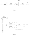


Classifications
-
- H—ELECTRICITY
- H05—ELECTRIC TECHNIQUES NOT OTHERWISE PROVIDED FOR
- H05B—ELECTRIC HEATING; ELECTRIC LIGHT SOURCES NOT OTHERWISE PROVIDED FOR; CIRCUIT ARRANGEMENTS FOR ELECTRIC LIGHT SOURCES, IN GENERAL
- H05B45/00—Circuit arrangements for operating light-emitting diodes [LED]
- H05B45/30—Driver circuits
- H05B45/357—Driver circuits specially adapted for retrofit LED light sources
- H05B45/3578—Emulating the electrical or functional characteristics of discharge lamps
-
- H—ELECTRICITY
- H05—ELECTRIC TECHNIQUES NOT OTHERWISE PROVIDED FOR
- H05B—ELECTRIC HEATING; ELECTRIC LIGHT SOURCES NOT OTHERWISE PROVIDED FOR; CIRCUIT ARRANGEMENTS FOR ELECTRIC LIGHT SOURCES, IN GENERAL
- H05B45/00—Circuit arrangements for operating light-emitting diodes [LED]
- H05B45/30—Driver circuits
- H05B45/37—Converter circuits
-
- H—ELECTRICITY
- H05—ELECTRIC TECHNIQUES NOT OTHERWISE PROVIDED FOR
- H05B—ELECTRIC HEATING; ELECTRIC LIGHT SOURCES NOT OTHERWISE PROVIDED FOR; CIRCUIT ARRANGEMENTS FOR ELECTRIC LIGHT SOURCES, IN GENERAL
- H05B45/00—Circuit arrangements for operating light-emitting diodes [LED]
- H05B45/50—Circuit arrangements for operating light-emitting diodes [LED] responsive to malfunctions or undesirable behaviour of LEDs; responsive to LED life; Protective circuits
-
- H—ELECTRICITY
- H05—ELECTRIC TECHNIQUES NOT OTHERWISE PROVIDED FOR
- H05B—ELECTRIC HEATING; ELECTRIC LIGHT SOURCES NOT OTHERWISE PROVIDED FOR; CIRCUIT ARRANGEMENTS FOR ELECTRIC LIGHT SOURCES, IN GENERAL
- H05B45/00—Circuit arrangements for operating light-emitting diodes [LED]
- H05B45/50—Circuit arrangements for operating light-emitting diodes [LED] responsive to malfunctions or undesirable behaviour of LEDs; responsive to LED life; Protective circuits
- H05B45/58—Circuit arrangements for operating light-emitting diodes [LED] responsive to malfunctions or undesirable behaviour of LEDs; responsive to LED life; Protective circuits involving end of life detection of LEDs
-
- H—ELECTRICITY
- H05—ELECTRIC TECHNIQUES NOT OTHERWISE PROVIDED FOR
- H05B—ELECTRIC HEATING; ELECTRIC LIGHT SOURCES NOT OTHERWISE PROVIDED FOR; CIRCUIT ARRANGEMENTS FOR ELECTRIC LIGHT SOURCES, IN GENERAL
- H05B45/00—Circuit arrangements for operating light-emitting diodes [LED]
- H05B45/30—Driver circuits
- H05B45/37—Converter circuits
- H05B45/3725—Switched mode power supply [SMPS]
- H05B45/39—Circuits containing inverter bridges
-
- Y—GENERAL TAGGING OF NEW TECHNOLOGICAL DEVELOPMENTS; GENERAL TAGGING OF CROSS-SECTIONAL TECHNOLOGIES SPANNING OVER SEVERAL SECTIONS OF THE IPC; TECHNICAL SUBJECTS COVERED BY FORMER USPC CROSS-REFERENCE ART COLLECTIONS [XRACs] AND DIGESTS
- Y02—TECHNOLOGIES OR APPLICATIONS FOR MITIGATION OR ADAPTATION AGAINST CLIMATE CHANGE
- Y02B—CLIMATE CHANGE MITIGATION TECHNOLOGIES RELATED TO BUILDINGS, e.g. HOUSING, HOUSE APPLIANCES OR RELATED END-USER APPLICATIONS
- Y02B20/00—Energy efficient lighting technologies, e.g. halogen lamps or gas discharge lamps
- Y02B20/30—Semiconductor lamps, e.g. solid state lamps [SSL] light emitting diodes [LED] or organic LED [OLED]
Definitions
- the present invention relates to the technical field of illumination, particularly to a light-emitting diode (LED) drive circuit and an LED lamp.
- LED light-emitting diode
- AC is the mains input. After passing through the electronic ballast, it outputs high-frequency AC voltage and AC current to the LED tube. Inside the LED tube, a filament analog circuit is used to simulate the impedance of the traditional fluorescent filament; a rectifier bridge is used to convert the high-frequency AC voltage and AC current into DC voltage and DC current; and then the power conversion circuit converts them into suitable voltage and current to illuminate LED particles.
- FIG. 2 is a schematic structural circuit diagram of the conventional LED drive circuit, in which a switch S1, a switch S2, a stopping capacitor Cb, a resonant inductor Lr and a resonant capacitor Cr belong to an internal circuit of the electronic ballast; the switches S1 and S2 form a half-bridge circuit, and high voltage bus voltage is subjected to high frequency conversion; the stopping capacitor Cb removes the DC portion of the high frequency voltage and converts it into an AC high frequency voltage signal; the resonant inductor Lr and the resonant capacitor Cr form a resonant cavity for resonant lighting when the fluorescent lamp is connected; and the resonant inductor Lr has current limiting function after stable operation.
- the LED tube is connected to the electronic ballast through terminals 1, 2, 3 and 4, passes through the filament analog circuit, and enters a rectifier bridge composed of diodes D1, D2, D3 and D4.
- the high frequency AC signal from the ballast is converted into a DC signal through the rectifier bridge and outputted to an LED light source through the power conversion circuit.
- the conventional LED tube When the conventional LED tube is connected to a constant-power electronic ballast or a magnetic ring self-excited electronic ballast, since the electronic ballast maintains the output of the power used by corresponding fluorescent lamp, the power is often much larger than the power of the LED tube. Overhigh power will cause the LED tube to trigger protection, overheat or be aged quickly, which can affect the use of the LED tube. If the tube is provided with a corresponding built-in protection, the LED tube will not be compatible with this type of electronic ballast, which will also affect the sales of products.
- the present invention provides an LED drive circuit and an LED lamp to overcome the problem or at least partially solve the above problem.
- One aspect of the present invention provides an LED drive circuit, which comprises: a feedback control circuit and a load impedance increasing circuit, wherein the feedback control circuit acquires the operating current of an LED, compares the operating current with a default threshold, drives the load impedance increasing circuit to operate when the operating current of the LED is greater than or equal to the threshold, and allows the load impedance increasing circuit not to operate when the operating current of the LED is less than the threshold; and the load equivalent impedance of the LED drive circuit is increased when the load impedance increasing circuit operates.
- the LED drive circuit further comprises: a rectifier bridge, wherein the load impedance increasing circuit is disposed between the rectifier bridge and the LED.
- the load impedance increasing circuit comprises: a load impedance increasing element and a switching element connected with the load impedance increasing element in parallel; when the switching element is switched on, the load impedance increasing element is bypassed; and when the switching element is switched off, the load impedance increasing element is connected to the LED drive circuit to increase the load equivalent impedance of the LED drive circuit.
- the switching element comprises: a power triode, a field effect transistor (FET) or a relay.
- FET field effect transistor
- the threshold is a threshold voltage
- the feedback control circuit comprises: a current detection unit, a threshold comparison unit and a drive unit, the current detection unit acquiring the operating current of the LED, converting the operating current into comparative voltage, and inputting the comparative voltage into the threshold comparison unit, and the threshold comparison unit comparing the comparative voltage with the threshold voltage, controlling the drive unit to start operating so as to drive the load impedance increasing circuit to operate when the comparative voltage is greater than or equal to the threshold voltage, and allowing the drive unit not to operate and allowing the load impedance increasing circuit not to operate when the comparative voltage is less than the threshold voltage.
- the current detection unit comprises: a sampling resistor, a transformer or a Hall sensor.
- the current detection unit comprises a sampling resistor, the sampling resistor being connected with the LED in series, and the comparative voltage being generated when the operating current of the LED flows across the sampling resistor.
- the threshold comparison unit comprises: a comparator, the sampling resistor being connected to a positive end of the comparator, the threshold voltage being connected to a negative end of the comparator, an output of the comparator being connected to the drive unit, and the output of the comparator being also connected to the positive end of the comparator.
- the threshold comparison unit further comprises: a first resistor, a second resistor, a third resistor and a fourth resistor, the sampling resistor being connected to the positive end of the comparator through the first resistor, the threshold voltage being connected to the negative end of the comparator through the second resistor, the output of the comparator being connected to the positive end of the comparator through the third resistor, and the output of the comparator being connected to the drive unit through the fourth resistor.
- the drive unit comprises: a switch triode, a current-limiting resistor and a fly-wheel diode, a base of the switch triode being connected to an output of the threshold comparison unit, an emitter of the switch triode being grounded, a collector of the switch triode being connected to the fly-wheel diode through the current-limiting resistor, and the fly-wheel diode being connected with the switching element of the load impedance increasing circuit in reverse parallel.
- the LED drive circuit further comprises a power conversion circuit;
- the load impedance increasing element is an impedance inductor;
- the switching element is a relay;
- the relay comprises a drive winding and a relay switch; one end of the drive winding is connected to the collector of the switch triode through the current-limiting resistor; the other end of the drive winding is connected to a power source; the drive winding is connected with the fly-wheel diode in reverse parallel; the relay switch is connected with the impedance inductor in parallel; and two ends of the impedance inductor are respectively connected with the rectifier bridge and the power conversion circuit.
- the LED drive circuit further comprises: a power conversion circuit; the drive unit comprises: an optical coupling module, a first divider resistor, a second divider resistor and a voltage regulator diode; an input of the optical coupling module is connected to an output of the threshold comparison unit; an output of the optical coupling module is connected to the load impedance increasing circuit; a bus of the rectifier bridge is connected to the switching element of the load impedance increasing circuit through the first divider resistor and the second divider resistor; and two ends of the voltage regulator diode are respectively connected with two ends of the switching element.
- the drive unit comprises: an optical coupling module, a first divider resistor, a second divider resistor and a voltage regulator diode; an input of the optical coupling module is connected to an output of the threshold comparison unit; an output of the optical coupling module is connected to the load impedance increasing circuit; a bus of the rectifier bridge is connected to the switching element of the load impedance increasing circuit through the first divider resistor and the second divider resist
- the load impedance increasing element is an impedance inductor;
- the switching element is an FET;
- the bus of the rectifier bridge is connected to a gate electrode of the FET through the first divider resistor and the second divider resistor;
- the gate electrode of the FET is also connected to the output of the optical coupling module;
- the gate electrode and a source electrode of the FET are respectively connected with two ends of the voltage regulator diode;
- two ends of the impedance inductor are respectively connected with the source electrode and a drain electrode of the FET; one end of the impedance inductor, connected with the source electrode of the FET, is also connected with the rectifier bridge; and one end of the impedance inductor, connected with the drain electrode of the FET, is also connected with the power conversion circuit.
- Another aspect of the present invention also provides an LED lamp, which comprises any foregoing LED drive circuit and at least one LED connected with the LED drive circuit.
- the LED drive circuit is configured to drive the at least one LED to emit light after power-on.
- the LED drive circuit provided by the embodiments of the present invention is applicable to the LED lamp compatible with the electronic ballast, especially for the constant-power ballast or the magnetic ring self-excited ballast, it can reduce the output power of the ballast, and can allow the LED lamp to work at a rated power to avoid the damage or premature decay of the LED lamp due to over-power usage.
- an LED drive circuit which can reduce the output power of an electronic ballast when it is connected to a constant-power electronic ballast or a magnetic ring self-excited electronic ballast, allow the LED tube to work within the design power, and ensure the normal use of the LED tube and the product life.
- FIG. 3 is a schematic diagram of an LED drive circuit provided by an embodiment of the present invention.
- the LED drive circuit provided by the embodiment of the present invention can directly cooperate with modules of the conventional LED drive circuit.
- the LED drive circuit provided by the embodiment of the present invention comprises a feedback control circuit 13 and a load impedance increasing circuit 14, which can directly cooperate with a filament analog circuit 10, a rectifier bridge 11 and a power conversion circuit 12.
- the entire LED drive circuit is used to drive at least one LED to emit light after power-on.
- FIG. 3 only shows one LED.
- the load impedance increasing circuit 14 can be disposed between the rectifier bridge 11 and the above LED.
- the feedback control circuit 13 acquires the operating current of the LED, compares the operating current with a default threshold, drives the load impedance increasing circuit 14 to operate when the operating current of the LED is greater than or equal to the threshold, and allows the load impedance increasing circuit 14 not to operate when the operating current of the LED is less than the threshold.
- the load equivalent impedance of the LED drive circuit is increased when the load impedance increasing circuit 14 operates.
- the LED drive circuit provided by the embodiment can improve the load equivalent impedance of the entire LED drive circuit when the LED power is overhigh, reduce the output current of the electronic ballast, and achieve the objective of reducing the output power.
- the LED drive circuit provided by the embodiment is applicable to an LED lamp/tube compatible with the electronic ballast, in particular to a constant-power ballast or a magnetic ring self-excited ballast, which can reduce the output power of the ballast, and allow the LED lamp to work at the rated power to avoid the damage or premature decay of the LED lamp due to over-power usage.
- the feedback control circuit 13 can be implemented by the following architecture. As shown in FIG. 4 , the feedback control circuit 13 may include: a current detection unit 131, a threshold comparison unit 132 and a drive unit 133.
- the current detection unit 131 acquires the operating current of the LED, converts the operating current into a comparative voltage, and inputs the comparative voltage into the threshold comparison unit 132.
- the threshold comparison unit 132 compares the comparative voltage with the threshold voltage, controls the drive unit 133 to start operating so as to drive the load impedance increasing circuit 14 to operate when the comparative voltage is greater than or equal to the threshold voltage, and allows the drive unit 133 not to operate and allows the load impedance increasing circuit 14 not to operate when the comparative voltage is less than the threshold voltage.
- the preferred embodiment provides a proposal for preferably implementing the feedback control circuit 13.
- the functions of the feedback control circuit 13 can be completely realized based on the current detection unit 131, the threshold comparison unit 132 and the drive unit 133.
- the architecture is simple and the control logic is clear.
- the proposal provided by the preferred embodiment adopts a way of comparison after the conversion of a current into a voltage, and can greatly simplify the circuit structure and reduce the cost. At this point, the above threshold is the voltage threshold.
- the current detection unit 131 can be directly implemented based on a sampling resistor, a transformer or a hall sensor, namely the function of acquiring a current can be implemented by adoption of a sampling resistor, a transformer or a Hall sensor.
- the load impedance increasing circuit 14 can be implemented through a load impedance increasing element 141 and a switching element 142 connected with the load impedance increasing element 141 in parallel.
- the switching element 142 is switched on, the load impedance increasing element 141 is bypassed, and the load equivalent impedance of the LED drive circuit does not change.
- the switching element 142 is switched off, the load impedance increasing element 141 is connected to the LED drive circuit to increase the load equivalent impedance of the LED drive circuit.
- the load impedance increasing circuit 14 can be disposed between the rectifier bridge 11 and the power conversion circuit 12.
- the load impedance increasing element 141 can be implemented by an inductor connected with the rectifier bridge 11 and the power conversion circuit 12 in series.
- the switching element 142 can be implemented by a power triode, an FET, or a relay.
- the switching element 142 is controlled by the LED current and is connected to the current detection unit 131 in the LED circuit, which inputs the comparison result into the drive unit 133 by a threshold comparison, and the drive unit 133 controls the 'on' and 'off' of the switching element 142.
- the current detection unit 131 can feed back the current of the LED. The current is compared with a default threshold.
- the drive unit 133 switches on the switching element 142, the load impedance increasing element 141 is shorted, and the operating state is unchanged.
- the drive unit 133 switches off the switch K, the load impedance increasing element 141 is connected between the rectifier bridge 11 and the power conversion circuit 12, and the load equivalent impedance of the LED drive circuit is increased.
- the current can be converted into a voltage for comparison, and at this point, it is needed to set the default threshold to be a threshold voltage.
- a voltage can be directly sampled in equal proportion through a divider resistor and then compared with the threshold voltage.
- the load impedance increasing element 141 can be implemented by an inductor.
- the electronic ballast outputs a high-frequency voltage and a high-frequency current, and the inductor reveals certain impedance under a high-frequency current.
- the impedance and the subsequent power conversion circuit form a connection in series, so the load equivalent impedance can be improved.
- the output current of electronic ballast can be reduced, and the objective of reducing the output power can be achieved.
- the load impedance characteristic can also be changed.
- the total harmonic distortion of the input current can be reduced.
- the circuit structure as shown in FIG. 5 can be established.
- the rectifier bridge 11 is composed of diodes D1, D2, D3 and D4; the load impedance increasing circuit 14 is disposed between the rectifier bridge 11 and the power conversion circuit 12, and it includes an inductor L and a relay K1; and the relay K1 is normally closed without excitation.
- the current detection unit 131 is implemented by a sampling resistor Rs; the current sampling resistor Rs is connected in series to the LED circuit; and a corresponding voltage, namely a comparative voltage, is generated when the LED current flows across the sampling resistor Rs.
- the threshold comparison unit 132 is implemented on the basis of a comparator U1.
- a first resistor R1, a second resistor R2, a third resistor Rfb and a fourth resistor Rd can be additionally arranged.
- the comparative voltage is fed back to a positive end of the comparator U1 through the first resistor R1; the threshold voltage Vref is connected to a negative end of the comparator U1 through the second resistor R2; an output of the comparator U1 is fed back to the positive end through the third resistor Rfb on one hand, and drives a switch triode Q1 of the drive unit 133 through the fourth resistor Rd on the other hand.
- a collector of the switch triode Q1 is connected to a drive winding of the relay K1 through a current-limiting resistor R3; R3 is used to limit the current flowing across the drive winding of the relay K1; and the other end of the drive winding is connected with a power source Vcc; and meanwhile, the drive winding is connected with a fly-wheel diode D4 in reverse parallel and used to provide the drive winding with a fly-wheel circuit when the switch triode Q1 is switched off.
- the relay K1 As the relay K1 is normally closed without excitation, after the circuit is powered on, the relay K1 remains closed, the inductor L is shorted, and the circuit operates normally. At this point, current flows into the LED and is detected by the sampling resistor Rs. If the current flowing into the LED is less than the default threshold, the negative end of the comparator U1 is larger than the positive end, the comparator U1 outputs a low level, the switch triode Q1 remains off, no exciting current flows across the drive winding of the relay K, and the relay K1 remains closed.
- the comparator U1 If the current flowing across the LED is larger than the default threshold, the negative end of the comparator U1 is smaller than the positive end, the comparator U1 outputs a high level, the switch triode Q1 is switched on, and the power source Vcc provides current which flows into the drive winding of the relay K1, so that the relay K1 is turned off, and the inductor L is connected in the circuit, so as to reduce the output power of the electronic ballast and reduce the current flowing into the LED.
- the third resistor Rfb is used for positive feedback.
- the comparator U1 outputs a high level, the high level is fed back to the positive end and inputted through the third resistor Rfb. Even though the comparative voltage fed back by the sampling resistor Rs is reduced due to the reduced LED current, due to the feedback of the third resistor Rfb, the positive end of the comparator U1 is larger than the negative end, and the comparator U1 maintains high level output.
- a circuit structure as shown in FIG. 6 can also be established.
- the load impedance increasing circuit 14 includes an inductor L and an FET K2; two ends of the inductor L1 are connected with the FET K2 in parallel; a gate electrode of the FET K2 drives a bus from the rectifier bridge 11; the bus is connected after being subjected to voltage dividing through the first divider resistor RA and the second divider resistor RB and is used to limit the driving voltage when the gate electrode and a source electrode of the FET K2 are connected to a voltage regulator diode Dz.
- the LED current is detected by the sampling resistor Rs and fed back to the positive end of the comparator U1; the threshold voltage Vref is connected to the negative end of the comparator U1 through the second resistor R2; an output of U1 is fed back to the positive end for input through the third resistor Rfb on one hand, and connected to an optical coupling module U2 through the fourth resistor Rd on the other hand; and the optical coupling module U2 is used to provide a drive 'off' signal to control the 'on' or 'off' of the FET K2.
- the bus voltage of the rectifier bridge provides a drive bias to the FET K2 through the first divider resistor RA and the second divider resistor RB, so that the FET K2 can be saturated and switched on.
- the comparator U1 outputs a low level, no drive current flows across the optical coupling module U2, the optical coupling module U2 remains 'off', the switch K remains 'on', so that the inductor L is bypassed, and the original work cannot be affected.
- the comparator U1 When the output power of the electronic ballast is overlarge, the current flowing across the LED is larger and exceeds the default threshold, the positive end of the comparator U1 is larger than the negative end, the comparator U1 outputs a high level and drives the optical coupling module U2.
- the conduction of the optical coupling module U2 reduces the voltage of the gate electrode of the FET K2, the FET K2 is switched off, the inductor L is connected to the circuit, and the output power of the electronic ballast is reduced.
- An embodiment of the present invention also provides an LED lamp, which comprises any foregoing LED drive circuit and at least one LED connected with the LED drive circuit.
- the LED drive circuit is used to drive the at least one LED to emit light after power-on.
- the embodiments of the present invention provide an LED drive circuit, which is applicable to an LED lamp compatible with an electronic ballast, in particular to a constant-power ballast or a magnetic ring self-excited ballast.
- the drive circuit can reduce the output power of the ballast, and allows the LED lamp to work at a rated power to avoid the damage or premature decay of the LED lamp due to over-power usage. Meanwhile, the drive circuit can further improve the harmonic distortion of the input current for electronic ballasts that adopt passive power factor correction.
- modules in the devices of the embodiments can be adaptively changed and disposed in one or more devices different from the embodiment.
- the modules, units or components in the embodiments can be combined into one module, one unit, or one component, and further can be divided into a plurality of sub-modules, sub-units, or sub-components. Except that at least some of such features and/or processes or units are mutually exclusive, all the features disclosed in the description (including the accompanying claims, abstract and drawings) or all the processes or units of any method or device so disclosed can be randomly combined. Unless otherwise specified, each feature disclosed in the description (including the accompanying claims, abstract and drawings) can be replaced by an alternative feature that provides the same, equivalent, or similar purpose.
- the component embodiments of the present invention can be implemented in hardware, or in a software module running on one or more processors, or in a combination thereof. It should be understood by those skilled in the art that a microprocessor or a digital signal processor (DSP) can be used in practice to implement some or all of the functions of some or all of the components in the LED driver circuit provided by the embodiments of the present invention.
- DSP digital signal processor
- the invention can also be implemented as a device or a device program (e.g., a computer program and a computer program product) for executing some or all of the methods described herein.
- Such a program for implementing the present invention can be stored on a computer readable medium or can be in the form of one or more signals. Such signals can be downloaded from the Internet website, or provided on the carrier signal, or provided in any other form.
- any reference numeral placed between parentheses shall not be construed as the limitation of the claims.
- the word “comprise” does not exclude the presence of the elements or steps that are not recited in the claims.
- the word “a” or “an” disposed before the element does not exclude the presence of a plurality of such elements.
- the present invention can be implemented by hardware comprising several distinct elements and by a suitably programmed computer. In the unit claims enumerating several devices, several of these devices can be specifically embodied by the same hardware item.
- the use of the words 'first,' 'second,' 'third' and the like does not indicate any order. These words can be interpreted as a name.
Landscapes
- Circuit Arrangement For Electric Light Sources In General (AREA)
Abstract
Description
- The present invention relates to the technical field of illumination, particularly to a light-emitting diode (LED) drive circuit and an LED lamp.
- The high luminous efficiency, long life and mercury-free characteristics of LEDs have made it a trend to replace the traditional fluorescent tubes with LED tubes. There are two main ways for this replacement application. One way is to completely remove the original fluorescent tube and ballast, and directly input the mains electricity to the LED tube. This method needs to modify the internal wiring of the lamps, additional labor cost is generated. The other way is only to replace the lamp tube. The mounted LED tube needs to be compatible with the original ballast. This kind of replacement is very simple and convenient, and a user can operate it himself without having to hire a professional person, which can eliminate the related labor cost.
- In fluorescent lamp ballasts, electronic ballasts occupy a considerable proportion, so a big challenge in replacing the fluorescent tubes is the compatibility with the electronic ballasts. Electronic ballasts have different topological structures. Moreover, as the used power of the LED tube is often much lower than the power of the fluorescent tube, there are many difficulties in making the electronic ballast cooperate with the LED tube. The current mainstream LED drive circuit architecture is as shown in
FIG.1 . - In
FIG. 1 , AC is the mains input. After passing through the electronic ballast, it outputs high-frequency AC voltage and AC current to the LED tube. Inside the LED tube, a filament analog circuit is used to simulate the impedance of the traditional fluorescent filament; a rectifier bridge is used to convert the high-frequency AC voltage and AC current into DC voltage and DC current; and then the power conversion circuit converts them into suitable voltage and current to illuminate LED particles. -
FIG. 2 is a schematic structural circuit diagram of the conventional LED drive circuit, in which a switch S1, a switch S2, a stopping capacitor Cb, a resonant inductor Lr and a resonant capacitor Cr belong to an internal circuit of the electronic ballast; the switches S1 and S2 form a half-bridge circuit, and high voltage bus voltage is subjected to high frequency conversion; the stopping capacitor Cb removes the DC portion of the high frequency voltage and converts it into an AC high frequency voltage signal; the resonant inductor Lr and the resonant capacitor Cr form a resonant cavity for resonant lighting when the fluorescent lamp is connected; and the resonant inductor Lr has current limiting function after stable operation. The LED tube is connected to the electronic ballast throughterminals - When the conventional LED tube is connected to a constant-power electronic ballast or a magnetic ring self-excited electronic ballast, since the electronic ballast maintains the output of the power used by corresponding fluorescent lamp, the power is often much larger than the power of the LED tube. Overhigh power will cause the LED tube to trigger protection, overheat or be aged quickly, which can affect the use of the LED tube. If the tube is provided with a corresponding built-in protection, the LED tube will not be compatible with this type of electronic ballast, which will also affect the sales of products.
- In view of the above problem, the present invention provides an LED drive circuit and an LED lamp to overcome the problem or at least partially solve the above problem.
- One aspect of the present invention provides an LED drive circuit, which comprises: a feedback control circuit and a load impedance increasing circuit, wherein the feedback control circuit acquires the operating current of an LED, compares the operating current with a default threshold, drives the load impedance increasing circuit to operate when the operating current of the LED is greater than or equal to the threshold, and allows the load impedance increasing circuit not to operate when the operating current of the LED is less than the threshold; and the load equivalent impedance of the LED drive circuit is increased when the load impedance increasing circuit operates.
- Optionally, the LED drive circuit further comprises: a rectifier bridge, wherein the load impedance increasing circuit is disposed between the rectifier bridge and the LED.
- Optionally, the load impedance increasing circuit comprises: a load impedance increasing element and a switching element connected with the load impedance increasing element in parallel; when the switching element is switched on, the load impedance increasing element is bypassed; and when the switching element is switched off, the load impedance increasing element is connected to the LED drive circuit to increase the load equivalent impedance of the LED drive circuit.
- Optionally, the switching element comprises: a power triode, a field effect transistor (FET) or a relay.
- Optionally, the threshold is a threshold voltage; the feedback control circuit comprises: a current detection unit, a threshold comparison unit and a drive unit, the current detection unit acquiring the operating current of the LED, converting the operating current into comparative voltage, and inputting the comparative voltage into the threshold comparison unit, and the threshold comparison unit comparing the comparative voltage with the threshold voltage, controlling the drive unit to start operating so as to drive the load impedance increasing circuit to operate when the comparative voltage is greater than or equal to the threshold voltage, and allowing the drive unit not to operate and allowing the load impedance increasing circuit not to operate when the comparative voltage is less than the threshold voltage.
- Optionally, the current detection unit comprises: a sampling resistor, a transformer or a Hall sensor.
- Optionally, the current detection unit comprises a sampling resistor, the sampling resistor being connected with the LED in series, and the comparative voltage being generated when the operating current of the LED flows across the sampling resistor.
- Optionally, the threshold comparison unit comprises: a comparator, the sampling resistor being connected to a positive end of the comparator, the threshold voltage being connected to a negative end of the comparator, an output of the comparator being connected to the drive unit, and the output of the comparator being also connected to the positive end of the comparator.
- Optionally, the threshold comparison unit further comprises: a first resistor, a second resistor, a third resistor and a fourth resistor, the sampling resistor being connected to the positive end of the comparator through the first resistor, the threshold voltage being connected to the negative end of the comparator through the second resistor, the output of the comparator being connected to the positive end of the comparator through the third resistor, and the output of the comparator being connected to the drive unit through the fourth resistor.
- Optionally, the drive unit comprises: a switch triode, a current-limiting resistor and a fly-wheel diode, a base of the switch triode being connected to an output of the threshold comparison unit, an emitter of the switch triode being grounded, a collector of the switch triode being connected to the fly-wheel diode through the current-limiting resistor, and the fly-wheel diode being connected with the switching element of the load impedance increasing circuit in reverse parallel.
- Optionally, the LED drive circuit further comprises a power conversion circuit; the load impedance increasing element is an impedance inductor; the switching element is a relay; the relay comprises a drive winding and a relay switch; one end of the drive winding is connected to the collector of the switch triode through the current-limiting resistor; the other end of the drive winding is connected to a power source; the drive winding is connected with the fly-wheel diode in reverse parallel; the relay switch is connected with the impedance inductor in parallel; and two ends of the impedance inductor are respectively connected with the rectifier bridge and the power conversion circuit.
- Optionally, the LED drive circuit further comprises: a power conversion circuit; the drive unit comprises: an optical coupling module, a first divider resistor, a second divider resistor and a voltage regulator diode; an input of the optical coupling module is connected to an output of the threshold comparison unit; an output of the optical coupling module is connected to the load impedance increasing circuit; a bus of the rectifier bridge is connected to the switching element of the load impedance increasing circuit through the first divider resistor and the second divider resistor; and two ends of the voltage regulator diode are respectively connected with two ends of the switching element.
- Optionally, the load impedance increasing element is an impedance inductor; the switching element is an FET; the bus of the rectifier bridge is connected to a gate electrode of the FET through the first divider resistor and the second divider resistor; the gate electrode of the FET is also connected to the output of the optical coupling module; the gate electrode and a source electrode of the FET are respectively connected with two ends of the voltage regulator diode; two ends of the impedance inductor are respectively connected with the source electrode and a drain electrode of the FET; one end of the impedance inductor, connected with the source electrode of the FET, is also connected with the rectifier bridge; and one end of the impedance inductor, connected with the drain electrode of the FET, is also connected with the power conversion circuit.
- Another aspect of the present invention also provides an LED lamp, which comprises any foregoing LED drive circuit and at least one LED connected with the LED drive circuit. The LED drive circuit is configured to drive the at least one LED to emit light after power-on.
- The LED drive circuit provided by the embodiments of the present invention is applicable to the LED lamp compatible with the electronic ballast, especially for the constant-power ballast or the magnetic ring self-excited ballast, it can reduce the output power of the ballast, and can allow the LED lamp to work at a rated power to avoid the damage or premature decay of the LED lamp due to over-power usage.
- The above description is only a brief description of the technical proposals of the present invention. In order to more clearly understand the technical means of the present invention, it can be implemented according to the content of the description. Moreover, the specific embodiments of the present invention will be described below for more clear understanding of the above and other objects, characteristics and advantages of the present invention.
- The above and other objects, advantages and characteristics of the present invention will become apparent to those skilled in the art according to the detailed description of the preferred embodiments of the present invention with reference to the accompanying drawings.
- Various other advantages and benefits will become apparent to one of ordinary skill in the art according to the following detailed description of the preferred embodiments. The drawings are only for the purpose of illustrating the preferred embodiments and are not to be construed as the limitation of the present invention. Throughout the drawings, the same reference numerals are used to refer to the same parts, in which,
-
FIG. 1 is a schematic diagram of a conventional LED drive circuit; -
FIG. 2 is a schematically structural circuit diagram of the conventional LED drive circuit; -
FIG. 3 is a schematic diagram of an LED drive circuit provided by an embodiment of the present invention; -
FIG. 4 is a schematic diagram of an LED drive circuit provided by a preferred embodiment of the present invention; -
FIG. 5 is a schematically structural circuit diagram of an LED drive circuit provided by a preferred embodiment of the present invention; and -
FIG. 6 is a schematically structural circuit diagram of an LED drive circuit provided by another preferred embodiment of the present invention. - Exemplary embodiments of the present invention will be described in detail below with reference to the accompanying drawings. Although the exemplary embodiments of the present invention have been shown in the drawings, it should be understood that the present invention can be implemented in various ways and should not be limited by the embodiments set forth herein. Rather, these embodiments are provided so that the invention can be more fully understood and the scope of the invention can be fully disclosed to those skilled in the art. It should be noted that the technical features in the embodiments and the preferred embodiments of the present invention can be combined with each other without conflict to each other.
- In view of the problems in the prior art, it is necessary to design an LED drive circuit, which can reduce the output power of an electronic ballast when it is connected to a constant-power electronic ballast or a magnetic ring self-excited electronic ballast, allow the LED tube to work within the design power, and ensure the normal use of the LED tube and the product life.
-
FIG. 3 is a schematic diagram of an LED drive circuit provided by an embodiment of the present invention. The LED drive circuit provided by the embodiment of the present invention can directly cooperate with modules of the conventional LED drive circuit. As shown inFIG. 3 , the LED drive circuit provided by the embodiment of the present invention comprises afeedback control circuit 13 and a loadimpedance increasing circuit 14, which can directly cooperate with a filamentanalog circuit 10, arectifier bridge 11 and apower conversion circuit 12. The entire LED drive circuit is used to drive at least one LED to emit light after power-on.FIG. 3 only shows one LED. Preferably, the loadimpedance increasing circuit 14 can be disposed between therectifier bridge 11 and the above LED. - In the embodiment, the
feedback control circuit 13 acquires the operating current of the LED, compares the operating current with a default threshold, drives the loadimpedance increasing circuit 14 to operate when the operating current of the LED is greater than or equal to the threshold, and allows the loadimpedance increasing circuit 14 not to operate when the operating current of the LED is less than the threshold. - The load equivalent impedance of the LED drive circuit is increased when the load
impedance increasing circuit 14 operates. - The LED drive circuit provided by the embodiment can improve the load equivalent impedance of the entire LED drive circuit when the LED power is overhigh, reduce the output current of the electronic ballast, and achieve the objective of reducing the output power. The LED drive circuit provided by the embodiment is applicable to an LED lamp/tube compatible with the electronic ballast, in particular to a constant-power ballast or a magnetic ring self-excited ballast, which can reduce the output power of the ballast, and allow the LED lamp to work at the rated power to avoid the damage or premature decay of the LED lamp due to over-power usage.
- In a preferred embodiment of the present invention, the
feedback control circuit 13 can be implemented by the following architecture. As shown inFIG. 4 , thefeedback control circuit 13 may include: acurrent detection unit 131, athreshold comparison unit 132 and adrive unit 133. Thecurrent detection unit 131 acquires the operating current of the LED, converts the operating current into a comparative voltage, and inputs the comparative voltage into thethreshold comparison unit 132. Thethreshold comparison unit 132 compares the comparative voltage with the threshold voltage, controls thedrive unit 133 to start operating so as to drive the loadimpedance increasing circuit 14 to operate when the comparative voltage is greater than or equal to the threshold voltage, and allows thedrive unit 133 not to operate and allows the loadimpedance increasing circuit 14 not to operate when the comparative voltage is less than the threshold voltage. - The preferred embodiment provides a proposal for preferably implementing the
feedback control circuit 13. The functions of thefeedback control circuit 13 can be completely realized based on thecurrent detection unit 131, thethreshold comparison unit 132 and thedrive unit 133. The architecture is simple and the control logic is clear. The proposal provided by the preferred embodiment adopts a way of comparison after the conversion of a current into a voltage, and can greatly simplify the circuit structure and reduce the cost. At this point, the above threshold is the voltage threshold. - In the above embodiment, the
current detection unit 131 can be directly implemented based on a sampling resistor, a transformer or a hall sensor, namely the function of acquiring a current can be implemented by adoption of a sampling resistor, a transformer or a Hall sensor. - Moreover, as shown in
FIG. 4 , the loadimpedance increasing circuit 14 can be implemented through a loadimpedance increasing element 141 and aswitching element 142 connected with the loadimpedance increasing element 141 in parallel. When theswitching element 142 is switched on, the loadimpedance increasing element 141 is bypassed, and the load equivalent impedance of the LED drive circuit does not change. When theswitching element 142 is switched off, the loadimpedance increasing element 141 is connected to the LED drive circuit to increase the load equivalent impedance of the LED drive circuit. - As shown in
FIG. 4 , the loadimpedance increasing circuit 14 can be disposed between therectifier bridge 11 and thepower conversion circuit 12. The loadimpedance increasing element 141 can be implemented by an inductor connected with therectifier bridge 11 and thepower conversion circuit 12 in series. The switchingelement 142 can be implemented by a power triode, an FET, or a relay. The switchingelement 142 is controlled by the LED current and is connected to thecurrent detection unit 131 in the LED circuit, which inputs the comparison result into thedrive unit 133 by a threshold comparison, and thedrive unit 133 controls the 'on' and 'off' of theswitching element 142. Thecurrent detection unit 131 can feed back the current of the LED. The current is compared with a default threshold. If the current flowing across the LED is less than the default threshold, thedrive unit 133 switches on theswitching element 142, the loadimpedance increasing element 141 is shorted, and the operating state is unchanged. When the current flowing across the LED is greater than the default threshold, thedrive unit 133 switches off the switch K, the loadimpedance increasing element 141 is connected between therectifier bridge 11 and thepower conversion circuit 12, and the load equivalent impedance of the LED drive circuit is increased. In the process of specifically comparing the operating current of the LED with the default threshold, the current can be converted into a voltage for comparison, and at this point, it is needed to set the default threshold to be a threshold voltage. In addition, a voltage can be directly sampled in equal proportion through a divider resistor and then compared with the threshold voltage. - The load
impedance increasing element 141 can be implemented by an inductor. As the electronic ballast outputs a high-frequency voltage and a high-frequency current, and the inductor reveals certain impedance under a high-frequency current. When the inductor is connected to the circuit, the impedance and the subsequent power conversion circuit form a connection in series, so the load equivalent impedance can be improved. In this way, the output current of electronic ballast can be reduced, and the objective of reducing the output power can be achieved. Meanwhile, due to the series connection between the inductor and the subsequent power conversion circuit, the load impedance characteristic can also be changed. For an electronic ballast adopting a similar charge pump manner to realize passive power factor correction, the total harmonic distortion of the input current can be reduced. - Based on the above circuit architecture, in a specific implementation, the circuit structure as shown in
FIG. 5 can be established. - As shown in
FIG. 5 , therectifier bridge 11 is composed of diodes D1, D2, D3 and D4; the loadimpedance increasing circuit 14 is disposed between therectifier bridge 11 and thepower conversion circuit 12, and it includes an inductor L and a relay K1; and the relay K1 is normally closed without excitation. Thecurrent detection unit 131 is implemented by a sampling resistor Rs; the current sampling resistor Rs is connected in series to the LED circuit; and a corresponding voltage, namely a comparative voltage, is generated when the LED current flows across the sampling resistor Rs. Thethreshold comparison unit 132 is implemented on the basis of a comparator U1. In addition, under the consideration of current limiting, a first resistor R1, a second resistor R2, a third resistor Rfb and a fourth resistor Rd can be additionally arranged. The comparative voltage is fed back to a positive end of the comparator U1 through the first resistor R1; the threshold voltage Vref is connected to a negative end of the comparator U1 through the second resistor R2; an output of the comparator U1 is fed back to the positive end through the third resistor Rfb on one hand, and drives a switch triode Q1 of thedrive unit 133 through the fourth resistor Rd on the other hand. A collector of the switch triode Q1 is connected to a drive winding of the relay K1 through a current-limiting resistor R3; R3 is used to limit the current flowing across the drive winding of the relay K1; and the other end of the drive winding is connected with a power source Vcc; and meanwhile, the drive winding is connected with a fly-wheel diode D4 in reverse parallel and used to provide the drive winding with a fly-wheel circuit when the switch triode Q1 is switched off. - As the relay K1 is normally closed without excitation, after the circuit is powered on, the relay K1 remains closed, the inductor L is shorted, and the circuit operates normally. At this point, current flows into the LED and is detected by the sampling resistor Rs. If the current flowing into the LED is less than the default threshold, the negative end of the comparator U1 is larger than the positive end, the comparator U1 outputs a low level, the switch triode Q1 remains off, no exciting current flows across the drive winding of the relay K, and the relay K1 remains closed. If the current flowing across the LED is larger than the default threshold, the negative end of the comparator U1 is smaller than the positive end, the comparator U1 outputs a high level, the switch triode Q1 is switched on, and the power source Vcc provides current which flows into the drive winding of the relay K1, so that the relay K1 is turned off, and the inductor L is connected in the circuit, so as to reduce the output power of the electronic ballast and reduce the current flowing into the LED.
- The third resistor Rfb is used for positive feedback. When the comparator U1 outputs a high level, the high level is fed back to the positive end and inputted through the third resistor Rfb. Even though the comparative voltage fed back by the sampling resistor Rs is reduced due to the reduced LED current, due to the feedback of the third resistor Rfb, the positive end of the comparator U1 is larger than the negative end, and the comparator U1 maintains high level output.
- Moreover, based on the above circuit architecture, in a specific implementation, a circuit structure as shown in
FIG. 6 can also be established. - In the circuit as shown in
FIG. 6 , thecurrent detection unit 131 and thethreshold comparison unit 132 have a same structure as thecurrent detection unit 131 and thethreshold comparison unit 132 in the circuit as shown inFIG. 5 . The loadimpedance increasing circuit 14 includes an inductor L and an FET K2; two ends of the inductor L1 are connected with the FET K2 in parallel; a gate electrode of the FET K2 drives a bus from therectifier bridge 11; the bus is connected after being subjected to voltage dividing through the first divider resistor RA and the second divider resistor RB and is used to limit the driving voltage when the gate electrode and a source electrode of the FET K2 are connected to a voltage regulator diode Dz. The LED current is detected by the sampling resistor Rs and fed back to the positive end of the comparator U1; the threshold voltage Vref is connected to the negative end of the comparator U1 through the second resistor R2; an output of U1 is fed back to the positive end for input through the third resistor Rfb on one hand, and connected to an optical coupling module U2 through the fourth resistor Rd on the other hand; and the optical coupling module U2 is used to provide a drive 'off' signal to control the 'on' or 'off' of the FET K2. - When the circuit is powered on, the bus voltage of the rectifier bridge provides a drive bias to the FET K2 through the first divider resistor RA and the second divider resistor RB, so that the FET K2 can be saturated and switched on. When the current flowing across the LED is not large, the comparative voltage fed back by the sampling resistor Rs is smaller than the voltage threshold Vref, the comparator U1 outputs a low level, no drive current flows across the optical coupling module U2, the optical coupling module U2 remains 'off', the switch K remains 'on', so that the inductor L is bypassed, and the original work cannot be affected. When the output power of the electronic ballast is overlarge, the current flowing across the LED is larger and exceeds the default threshold, the positive end of the comparator U1 is larger than the negative end, the comparator U1 outputs a high level and drives the optical coupling module U2. The conduction of the optical coupling module U2 reduces the voltage of the gate electrode of the FET K2, the FET K2 is switched off, the inductor L is connected to the circuit, and the output power of the electronic ballast is reduced.
- An embodiment of the present invention also provides an LED lamp, which comprises any foregoing LED drive circuit and at least one LED connected with the LED drive circuit. The LED drive circuit is used to drive the at least one LED to emit light after power-on.
- The embodiments of the present invention provide an LED drive circuit, which is applicable to an LED lamp compatible with an electronic ballast, in particular to a constant-power ballast or a magnetic ring self-excited ballast. The drive circuit can reduce the output power of the ballast, and allows the LED lamp to work at a rated power to avoid the damage or premature decay of the LED lamp due to over-power usage. Meanwhile, the drive circuit can further improve the harmonic distortion of the input current for electronic ballasts that adopt passive power factor correction.
- In the description provided herein, numerous specific details are set forth. However, it should be understood that the embodiments of the present invention can be practiced without these specific details. In some examples, well-known methods, structures and techniques have not been shown in detail so as not to obscure the understanding of the description.
- Similarly, it should be understood that, in order to simplify the present invention and help understanding one or more of various aspects of the present invention, in the above description of the exemplary embodiments of the present invention, the features of the present invention are sometimes grouped together into a single embodiment, drawing, or description thereof. However, the disclosed method is not to be interpreted as reflecting the following intention that the claimed invention requires more features than those specifically recited in the claims. More accurately, as the following claims reflect, the inventive aspects reside in less than all of features of a single embodiment disclosed above. Therefore, the claims following the specific embodiments are hereby explicitly incorporated into the specific embodiments, wherein each claim is itself a separate embodiment of the present invention.
- It should be understood by those skilled in the art that the modules in the devices of the embodiments can be adaptively changed and disposed in one or more devices different from the embodiment. The modules, units or components in the embodiments can be combined into one module, one unit, or one component, and further can be divided into a plurality of sub-modules, sub-units, or sub-components. Except that at least some of such features and/or processes or units are mutually exclusive, all the features disclosed in the description (including the accompanying claims, abstract and drawings) or all the processes or units of any method or device so disclosed can be randomly combined. Unless otherwise specified, each feature disclosed in the description (including the accompanying claims, abstract and drawings) can be replaced by an alternative feature that provides the same, equivalent, or similar purpose.
- Moreover, it should be understood by those skilled in the art that although some embodiments described herein include some features but not other features that are not included in other embodiments, the combinations of the features of different embodiments are intended to fall within the scope of the present invention and form different embodiments. For example, in the claims, any one of the claimed embodiments can be used in any combination.
- The component embodiments of the present invention can be implemented in hardware, or in a software module running on one or more processors, or in a combination thereof. It should be understood by those skilled in the art that a microprocessor or a digital signal processor (DSP) can be used in practice to implement some or all of the functions of some or all of the components in the LED driver circuit provided by the embodiments of the present invention. The invention can also be implemented as a device or a device program (e.g., a computer program and a computer program product) for executing some or all of the methods described herein. Such a program for implementing the present invention can be stored on a computer readable medium or can be in the form of one or more signals. Such signals can be downloaded from the Internet website, or provided on the carrier signal, or provided in any other form.
- It is to be noted that the above embodiments are illustrative of the present invention and are not intended to limit the present invention, and that alternative embodiments can be designed by those skilled in the art without departing from the scope of the appended claims. In the claims, any reference numeral placed between parentheses shall not be construed as the limitation of the claims. The word "comprise" does not exclude the presence of the elements or steps that are not recited in the claims. The word "a" or "an" disposed before the element does not exclude the presence of a plurality of such elements. The present invention can be implemented by hardware comprising several distinct elements and by a suitably programmed computer. In the unit claims enumerating several devices, several of these devices can be specifically embodied by the same hardware item. The use of the words 'first,' 'second,' 'third' and the like does not indicate any order. These words can be interpreted as a name.
- It will be appreciated by those skilled in the art that although a plurality of exemplary embodiments of the present invention have been shown and described herein, many other variations or modifications in accordance with the principle of the present invention can be directly determined or deduced according to the content disclosed in the present invention without departing from the spirit and the scope of the present invention. So, the scope of the present invention should be understood and construed as covering all such other variations or modifications.
Claims (14)
- A light-emitting diode (LED) drive circuit, comprising: a feedback control circuit and a load impedance increasing circuit, wherein
the feedback control circuit acquires operating current of an LED, compares the operating current with a default threshold, drives the load impedance increasing circuit to operate when the operating current of the LED is greater than or equal to the threshold, and allows the load impedance increasing circuit not to operate when the operating current of the LED is less than the threshold; and
the load equivalent impedance of the LED drive circuit is increased when the load impedance increasing circuit operates. - The LED drive circuit according to claim 1, further comprising: a rectifier bridge, wherein the load impedance increasing circuit is disposed between the rectifier bridge and the LED.
- The LED drive circuit according to claim 2, wherein the load impedance increasing circuit comprises a load impedance increasing element and a switching element connected with the load impedance increasing element in parallel; when the switching element is switched on, the load impedance increasing element is bypassed; and when the switching element is switched off, the load impedance increasing element is connected to the LED drive circuit to increase the load equivalent impedance of the LED drive circuit.
- The LED drive circuit according to claim 3, wherein the switching element comprises: a power triode, a field effect transistor (FET) or a relay.
- The LED drive circuit according to claim 3, wherein the threshold is threshold voltage; the feedback control circuit comprises a current detection unit, a threshold comparison unit and a drive unit, the current detection unit acquiring the operating current of the LED, converting the operating current into comparative voltage, and inputting the comparative voltage into the threshold comparison unit, and the threshold comparison unit comparing the comparative voltage with the threshold voltage, controlling the drive unit to start operating so as to drive the load impedance increasing circuit to operate when the comparative voltage is greater than or equal to the threshold voltage, and allowing the drive unit not to operate and allowing the load impedance increasing circuit not to operate when the comparative voltage is less than the threshold voltage.
- The LED drive circuit according to claim 5, wherein the current detection unit comprises: a sampling resistor, a transformer or a Hall sensor.
- The LED drive circuit according to claim 6, wherein the current detection unit comprises a sampling resistor, the sampling resistor being connected with the LED in series, and the comparative voltage being generated when the operating current of the LED flows across the sampling resistor.
- The LED drive circuit according to claim 7, wherein the threshold comparison unit comprises a comparator, the sampling resistor being connected to a positive end of the comparator, the threshold voltage being connected to a negative end of the comparator, an output of the comparator being connected to the drive unit, and the output of the comparator being also connected to the positive end of the comparator.
- The LED drive circuit according to claim 8, wherein the threshold comparison unit further comprises: a first resistor, a second resistor, a third resistor and a fourth resistor, the sampling resistor being connected to the positive end of the comparator through the first resistor, the threshold voltage being connected to the negative end of the comparator through the second resistor, the output of the comparator being connected to the positive end of the comparator through the third resistor, and the output of the comparator being connected to the drive unit through the fourth resistor.
- The LED drive circuit according to claim 5, wherein the drive unit comprises: a switch triode, a current-limiting resistor and a fly-wheel diode, a base of the switch triode being connected to an output of the threshold comparison unit, an emitter of the switch triode being grounded, a collector of the switch triode being connected to the fly-wheel diode through the current-limiting resistor, and the fly-wheel diode being connected with the switching element of the load impedance increasing circuit in reverse parallel.
- The LED drive circuit according to claim 10, further comprising a power conversion circuit,
wherein the load impedance increasing element is an impedance inductor; the switching element is a relay, the relay comprising a drive winding and a relay switch, one end of the drive winding being connected to the collector of the switch triode through the current-limiting resistor, the other end of the drive winding being connected to a power source, the drive winding being connected with the fly-wheel diode in reverse parallel, the relay switch being connected with the impedance inductor in parallel, and two ends of the impedance inductor being respectively connected with the rectifier bridge and the power conversion circuit. - The LED drive circuit according to claim 5, further comprising a power conversion circuit,
wherein the drive unit comprises: an optical coupling module, a first divider resistor, a second divider resistor and a voltage regulator diode, an input of the optical coupling module being connected to an output of the threshold comparison unit, an output of the optical coupling module being connected to the load impedance increasing circuit, a bus of the rectifier bridge being connected to the switching element of the load impedance increasing circuit through the first divider resistor and the second divider resistor, and two ends of the voltage regulator diode being respectively connected with two ends of the switching element. - The LED drive circuit according to claim 12, wherein the load impedance increasing element is an impedance inductor, and the switching element is an FET, the bus of the rectifier bridge being connected to a gate electrode of the FET through the first divider resistor and the second divider resistor, the gate electrode of the FET being also connected to the output of the optical coupling module, the gate electrode and a source electrode of the FET being respectively connected with two ends of the voltage regulator diode, two ends of the impedance inductor being respectively connected with the source electrode and a drain electrode of the FET, and one end of the impedance inductor, connected with the source electrode of the FET, is also connected with the rectifier bridge; and another end of the impedance inductor, connected with the drain electrode of the FET, is also connected with the power conversion circuit.
- An LED lamp, comprising the LED drive circuit according to any one of claims 1 to 11 and at least one LED connected with the LED drive circuit, wherein the LED drive circuit is configured to drive the at least one LED to emit light after power-on.
Applications Claiming Priority (3)
| Application Number | Priority Date | Filing Date | Title |
|---|---|---|---|
| CN201620828330.4U CN206196082U (en) | 2016-08-02 | 2016-08-02 | LED drive circuit and LED fluorescent tube |
| CN201610626520.2A CN106102253B (en) | 2016-08-02 | 2016-08-02 | LED driver circuit and LED tube |
| PCT/CN2017/095673 WO2018024220A1 (en) | 2016-08-02 | 2017-08-02 | Led drive circuit and led lamp |
Publications (3)
| Publication Number | Publication Date |
|---|---|
| EP3481159A1 true EP3481159A1 (en) | 2019-05-08 |
| EP3481159A4 EP3481159A4 (en) | 2019-05-08 |
| EP3481159B1 EP3481159B1 (en) | 2022-04-13 |
Family
ID=61073213
Family Applications (1)
| Application Number | Title | Priority Date | Filing Date |
|---|---|---|---|
| EP17836402.2A Active EP3481159B1 (en) | 2016-08-02 | 2017-08-02 | Led drive circuit and led lamp |
Country Status (3)
| Country | Link |
|---|---|
| US (1) | US10645775B2 (en) |
| EP (1) | EP3481159B1 (en) |
| WO (1) | WO2018024220A1 (en) |
Families Citing this family (4)
| Publication number | Priority date | Publication date | Assignee | Title |
|---|---|---|---|---|
| EP3481158B1 (en) * | 2016-08-02 | 2021-04-14 | Opple Lighting Co., Ltd. | Electronic ballast-based apparatus for controlling electronic control circuit and illuminating lamp |
| CN109788599A (en) * | 2017-11-14 | 2019-05-21 | 通用电气照明解决方案有限公司 | The protection circuit of LED light |
| CN110351920B (en) * | 2018-04-08 | 2022-05-27 | 朗德万斯公司 | Driver and lighting module |
| US20210126523A1 (en) * | 2020-01-19 | 2021-04-29 | Tong Chen | Electric power conversion system |
Family Cites Families (16)
| Publication number | Priority date | Publication date | Assignee | Title |
|---|---|---|---|---|
| ES2569057T3 (en) * | 2002-12-19 | 2016-05-06 | Koninklijke Philips N.V. | LED power supply |
| US8664880B2 (en) * | 2009-01-21 | 2014-03-04 | Ilumisys, Inc. | Ballast/line detection circuit for fluorescent replacement lamps |
| US20110089853A1 (en) * | 2009-10-17 | 2011-04-21 | General Electric Company | Electronic driver apparatus for large area solid-state leds |
| CN102595736B (en) * | 2012-03-01 | 2014-09-17 | 杭州乐图光电科技有限公司 | LED (Light-Emitting Diode) driving power supply compatible to electronic ballast |
| US9801241B2 (en) | 2012-06-15 | 2017-10-24 | Lightel Technologies, Inc. | Solid-state lighting without operational uncertainty and free of fire hazard |
| US9288867B2 (en) | 2012-06-15 | 2016-03-15 | Lightel Technologies, Inc. | Linear solid-state lighting with a wide range of input voltage and frequency free of fire and shock hazards |
| US9544959B2 (en) | 2012-06-15 | 2017-01-10 | Lightel Technologies, Inc. | Solid-state lighting compatible with ballasts and operable with AC mains |
| US9420663B1 (en) | 2015-04-16 | 2016-08-16 | Aleddra Inc. | Linear solid-state lighting with an arc prevention switch mechanism free of fire and shock hazards |
| JP6326309B2 (en) * | 2014-07-02 | 2018-05-16 | ルネサスエレクトロニクス株式会社 | Isolator, semiconductor device, and control method of isolator |
| US9763289B2 (en) * | 2015-03-31 | 2017-09-12 | Infineon Technologies Austria Ag | System and method for a switched-mode power supply |
| WO2016178727A1 (en) * | 2015-04-16 | 2016-11-10 | Lightel Technologies, Inc. | Linear solid-state lighting with a wide range of input voltage and frequency free of fire and shock hazards |
| CN104797058B (en) * | 2015-04-30 | 2018-12-14 | 杰华特微电子(杭州)有限公司 | Damping circuit and LED drive circuit with damping circuit |
| TWI591952B (en) * | 2015-05-15 | 2017-07-11 | 立錡科技股份有限公司 | Resonant wireless power receiver circuit and control circuit and wireless power conversion method thereof |
| CN205124089U (en) * | 2015-11-26 | 2016-03-30 | 欧普照明股份有限公司 | LED drive circuit and LED lamp |
| CN106102253B (en) * | 2016-08-02 | 2019-06-25 | 欧普照明股份有限公司 | LED driver circuit and LED tube |
| CN206196082U (en) * | 2016-08-02 | 2017-05-24 | 欧普照明股份有限公司 | LED drive circuit and LED fluorescent tube |
-
2017
- 2017-08-02 WO PCT/CN2017/095673 patent/WO2018024220A1/en not_active Ceased
- 2017-08-02 EP EP17836402.2A patent/EP3481159B1/en active Active
-
2019
- 2019-02-02 US US16/266,014 patent/US10645775B2/en active Active
Also Published As
| Publication number | Publication date |
|---|---|
| US10645775B2 (en) | 2020-05-05 |
| EP3481159A4 (en) | 2019-05-08 |
| WO2018024220A1 (en) | 2018-02-08 |
| EP3481159B1 (en) | 2022-04-13 |
| US20190174596A1 (en) | 2019-06-06 |
Similar Documents
| Publication | Publication Date | Title |
|---|---|---|
| JP5830986B2 (en) | Lighting control circuit, illumination lamp using the lighting control circuit, and luminaire using the illumination lamp | |
| US8242703B2 (en) | Driving apparatus for light emitting diodes without employing electrolytic capacitor | |
| KR100953325B1 (en) | Led lighting apparatus | |
| US10645775B2 (en) | LED drive circuit and LED lamp | |
| JP5156036B2 (en) | LED lighting device | |
| TW201249256A (en) | Frequency-variable dimming control apparatus for light-emitting diodes and method for operating the same | |
| US9385621B2 (en) | Stabilization circuit for low-voltage lighting | |
| CN106102253B (en) | LED driver circuit and LED tube | |
| JP2010140827A (en) | Lighting device and illumination fixture using the same | |
| JP2011216316A (en) | Led lighting device, and led luminaire | |
| EP2362717A3 (en) | Lighting Device and Illumination Fixture using thereof | |
| TWI466592B (en) | Light-emitting element lamp circuit | |
| CN102789763A (en) | Variable-frequency dimming control device of light emitting diode and operation method thereof | |
| WO2013171952A1 (en) | Lighting device and illumination device | |
| CN206196082U (en) | LED drive circuit and LED fluorescent tube | |
| TWI459862B (en) | Replacement electronic ballast lamp | |
| JP6167455B2 (en) | LED driving device and lighting apparatus | |
| CN102177766B (en) | Driver circuit for a semiconductor light source (led) | |
| CN110113842A (en) | Environment photoinduction controls lamp switch circuit | |
| US20170127488A1 (en) | Adaptive Power Balancing in LED Lamps | |
| US20190200426A1 (en) | Led lighting assembly and drive circuit | |
| JP5622618B2 (en) | LED power supply | |
| CN202425173U (en) | A long-life electrode type light lamp circuit | |
| JP2011070832A (en) | Lighting device | |
| CN2774072Y (en) | Circuit of electromagnetic induction light |
Legal Events
| Date | Code | Title | Description |
|---|---|---|---|
| STAA | Information on the status of an ep patent application or granted ep patent |
Free format text: STATUS: THE INTERNATIONAL PUBLICATION HAS BEEN MADE |
|
| PUAI | Public reference made under article 153(3) epc to a published international application that has entered the european phase |
Free format text: ORIGINAL CODE: 0009012 |
|
| STAA | Information on the status of an ep patent application or granted ep patent |
Free format text: STATUS: REQUEST FOR EXAMINATION WAS MADE |
|
| 17P | Request for examination filed |
Effective date: 20190201 |
|
| A4 | Supplementary search report drawn up and despatched |
Effective date: 20190404 |
|
| AK | Designated contracting states |
Kind code of ref document: A1 Designated state(s): AL AT BE BG CH CY CZ DE DK EE ES FI FR GB GR HR HU IE IS IT LI LT LU LV MC MK MT NL NO PL PT RO RS SE SI SK SM TR |
|
| AX | Request for extension of the european patent |
Extension state: BA ME |
|
| DAV | Request for validation of the european patent (deleted) | ||
| DAX | Request for extension of the european patent (deleted) | ||
| STAA | Information on the status of an ep patent application or granted ep patent |
Free format text: STATUS: EXAMINATION IS IN PROGRESS |
|
| 17Q | First examination report despatched |
Effective date: 20200213 |
|
| REG | Reference to a national code |
Ref country code: DE Ref legal event code: R079 Ref document number: 602017056034 Country of ref document: DE Free format text: PREVIOUS MAIN CLASS: H05B0037020000 Ipc: H05B0045357800 |
|
| GRAP | Despatch of communication of intention to grant a patent |
Free format text: ORIGINAL CODE: EPIDOSNIGR1 |
|
| STAA | Information on the status of an ep patent application or granted ep patent |
Free format text: STATUS: GRANT OF PATENT IS INTENDED |
|
| RIC1 | Information provided on ipc code assigned before grant |
Ipc: H05B 45/37 20200101ALI20211208BHEP Ipc: H05B 45/50 20200101ALI20211208BHEP Ipc: H05B 45/3578 20200101AFI20211208BHEP |
|
| INTG | Intention to grant announced |
Effective date: 20211222 |
|
| GRAS | Grant fee paid |
Free format text: ORIGINAL CODE: EPIDOSNIGR3 |
|
| GRAA | (expected) grant |
Free format text: ORIGINAL CODE: 0009210 |
|
| STAA | Information on the status of an ep patent application or granted ep patent |
Free format text: STATUS: THE PATENT HAS BEEN GRANTED |
|
| AK | Designated contracting states |
Kind code of ref document: B1 Designated state(s): AL AT BE BG CH CY CZ DE DK EE ES FI FR GB GR HR HU IE IS IT LI LT LU LV MC MK MT NL NO PL PT RO RS SE SI SK SM TR |
|
| REG | Reference to a national code |
Ref country code: GB Ref legal event code: FG4D |
|
| REG | Reference to a national code |
Ref country code: CH Ref legal event code: EP |
|
| REG | Reference to a national code |
Ref country code: DE Ref legal event code: R096 Ref document number: 602017056034 Country of ref document: DE |
|
| REG | Reference to a national code |
Ref country code: IE Ref legal event code: FG4D |
|
| REG | Reference to a national code |
Ref country code: AT Ref legal event code: REF Ref document number: 1484417 Country of ref document: AT Kind code of ref document: T Effective date: 20220515 |
|
| REG | Reference to a national code |
Ref country code: NL Ref legal event code: FP |
|
| REG | Reference to a national code |
Ref country code: LT Ref legal event code: MG9D |
|
| REG | Reference to a national code |
Ref country code: AT Ref legal event code: MK05 Ref document number: 1484417 Country of ref document: AT Kind code of ref document: T Effective date: 20220413 |
|
| PG25 | Lapsed in a contracting state [announced via postgrant information from national office to epo] |
Ref country code: SE Free format text: LAPSE BECAUSE OF FAILURE TO SUBMIT A TRANSLATION OF THE DESCRIPTION OR TO PAY THE FEE WITHIN THE PRESCRIBED TIME-LIMIT Effective date: 20220413 Ref country code: PT Free format text: LAPSE BECAUSE OF FAILURE TO SUBMIT A TRANSLATION OF THE DESCRIPTION OR TO PAY THE FEE WITHIN THE PRESCRIBED TIME-LIMIT Effective date: 20220816 Ref country code: NO Free format text: LAPSE BECAUSE OF FAILURE TO SUBMIT A TRANSLATION OF THE DESCRIPTION OR TO PAY THE FEE WITHIN THE PRESCRIBED TIME-LIMIT Effective date: 20220713 Ref country code: LT Free format text: LAPSE BECAUSE OF FAILURE TO SUBMIT A TRANSLATION OF THE DESCRIPTION OR TO PAY THE FEE WITHIN THE PRESCRIBED TIME-LIMIT Effective date: 20220413 Ref country code: HR Free format text: LAPSE BECAUSE OF FAILURE TO SUBMIT A TRANSLATION OF THE DESCRIPTION OR TO PAY THE FEE WITHIN THE PRESCRIBED TIME-LIMIT Effective date: 20220413 Ref country code: GR Free format text: LAPSE BECAUSE OF FAILURE TO SUBMIT A TRANSLATION OF THE DESCRIPTION OR TO PAY THE FEE WITHIN THE PRESCRIBED TIME-LIMIT Effective date: 20220714 Ref country code: FI Free format text: LAPSE BECAUSE OF FAILURE TO SUBMIT A TRANSLATION OF THE DESCRIPTION OR TO PAY THE FEE WITHIN THE PRESCRIBED TIME-LIMIT Effective date: 20220413 Ref country code: ES Free format text: LAPSE BECAUSE OF FAILURE TO SUBMIT A TRANSLATION OF THE DESCRIPTION OR TO PAY THE FEE WITHIN THE PRESCRIBED TIME-LIMIT Effective date: 20220413 Ref country code: BG Free format text: LAPSE BECAUSE OF FAILURE TO SUBMIT A TRANSLATION OF THE DESCRIPTION OR TO PAY THE FEE WITHIN THE PRESCRIBED TIME-LIMIT Effective date: 20220713 Ref country code: AT Free format text: LAPSE BECAUSE OF FAILURE TO SUBMIT A TRANSLATION OF THE DESCRIPTION OR TO PAY THE FEE WITHIN THE PRESCRIBED TIME-LIMIT Effective date: 20220413 |
|
| PG25 | Lapsed in a contracting state [announced via postgrant information from national office to epo] |
Ref country code: RS Free format text: LAPSE BECAUSE OF FAILURE TO SUBMIT A TRANSLATION OF THE DESCRIPTION OR TO PAY THE FEE WITHIN THE PRESCRIBED TIME-LIMIT Effective date: 20220413 Ref country code: PL Free format text: LAPSE BECAUSE OF FAILURE TO SUBMIT A TRANSLATION OF THE DESCRIPTION OR TO PAY THE FEE WITHIN THE PRESCRIBED TIME-LIMIT Effective date: 20220413 Ref country code: LV Free format text: LAPSE BECAUSE OF FAILURE TO SUBMIT A TRANSLATION OF THE DESCRIPTION OR TO PAY THE FEE WITHIN THE PRESCRIBED TIME-LIMIT Effective date: 20220413 Ref country code: IS Free format text: LAPSE BECAUSE OF FAILURE TO SUBMIT A TRANSLATION OF THE DESCRIPTION OR TO PAY THE FEE WITHIN THE PRESCRIBED TIME-LIMIT Effective date: 20220813 |
|
| REG | Reference to a national code |
Ref country code: DE Ref legal event code: R097 Ref document number: 602017056034 Country of ref document: DE |
|
| PG25 | Lapsed in a contracting state [announced via postgrant information from national office to epo] |
Ref country code: SM Free format text: LAPSE BECAUSE OF FAILURE TO SUBMIT A TRANSLATION OF THE DESCRIPTION OR TO PAY THE FEE WITHIN THE PRESCRIBED TIME-LIMIT Effective date: 20220413 Ref country code: SK Free format text: LAPSE BECAUSE OF FAILURE TO SUBMIT A TRANSLATION OF THE DESCRIPTION OR TO PAY THE FEE WITHIN THE PRESCRIBED TIME-LIMIT Effective date: 20220413 Ref country code: RO Free format text: LAPSE BECAUSE OF FAILURE TO SUBMIT A TRANSLATION OF THE DESCRIPTION OR TO PAY THE FEE WITHIN THE PRESCRIBED TIME-LIMIT Effective date: 20220413 Ref country code: EE Free format text: LAPSE BECAUSE OF FAILURE TO SUBMIT A TRANSLATION OF THE DESCRIPTION OR TO PAY THE FEE WITHIN THE PRESCRIBED TIME-LIMIT Effective date: 20220413 Ref country code: DK Free format text: LAPSE BECAUSE OF FAILURE TO SUBMIT A TRANSLATION OF THE DESCRIPTION OR TO PAY THE FEE WITHIN THE PRESCRIBED TIME-LIMIT Effective date: 20220413 Ref country code: CZ Free format text: LAPSE BECAUSE OF FAILURE TO SUBMIT A TRANSLATION OF THE DESCRIPTION OR TO PAY THE FEE WITHIN THE PRESCRIBED TIME-LIMIT Effective date: 20220413 |
|
| PLBE | No opposition filed within time limit |
Free format text: ORIGINAL CODE: 0009261 |
|
| STAA | Information on the status of an ep patent application or granted ep patent |
Free format text: STATUS: NO OPPOSITION FILED WITHIN TIME LIMIT |
|
| 26N | No opposition filed |
Effective date: 20230116 |
|
| PG25 | Lapsed in a contracting state [announced via postgrant information from national office to epo] |
Ref country code: MC Free format text: LAPSE BECAUSE OF FAILURE TO SUBMIT A TRANSLATION OF THE DESCRIPTION OR TO PAY THE FEE WITHIN THE PRESCRIBED TIME-LIMIT Effective date: 20220413 Ref country code: AL Free format text: LAPSE BECAUSE OF FAILURE TO SUBMIT A TRANSLATION OF THE DESCRIPTION OR TO PAY THE FEE WITHIN THE PRESCRIBED TIME-LIMIT Effective date: 20220413 |
|
| REG | Reference to a national code |
Ref country code: CH Ref legal event code: PL |
|
| PG25 | Lapsed in a contracting state [announced via postgrant information from national office to epo] |
Ref country code: LU Free format text: LAPSE BECAUSE OF NON-PAYMENT OF DUE FEES Effective date: 20220802 Ref country code: LI Free format text: LAPSE BECAUSE OF NON-PAYMENT OF DUE FEES Effective date: 20220831 Ref country code: CH Free format text: LAPSE BECAUSE OF NON-PAYMENT OF DUE FEES Effective date: 20220831 |
|
| PG25 | Lapsed in a contracting state [announced via postgrant information from national office to epo] |
Ref country code: SI Free format text: LAPSE BECAUSE OF FAILURE TO SUBMIT A TRANSLATION OF THE DESCRIPTION OR TO PAY THE FEE WITHIN THE PRESCRIBED TIME-LIMIT Effective date: 20220413 |
|
| PG25 | Lapsed in a contracting state [announced via postgrant information from national office to epo] |
Ref country code: IE Free format text: LAPSE BECAUSE OF NON-PAYMENT OF DUE FEES Effective date: 20220802 |
|
| PG25 | Lapsed in a contracting state [announced via postgrant information from national office to epo] |
Ref country code: IT Free format text: LAPSE BECAUSE OF FAILURE TO SUBMIT A TRANSLATION OF THE DESCRIPTION OR TO PAY THE FEE WITHIN THE PRESCRIBED TIME-LIMIT Effective date: 20220413 |
|
| PG25 | Lapsed in a contracting state [announced via postgrant information from national office to epo] |
Ref country code: HU Free format text: LAPSE BECAUSE OF FAILURE TO SUBMIT A TRANSLATION OF THE DESCRIPTION OR TO PAY THE FEE WITHIN THE PRESCRIBED TIME-LIMIT; INVALID AB INITIO Effective date: 20170802 |
|
| PG25 | Lapsed in a contracting state [announced via postgrant information from national office to epo] |
Ref country code: MK Free format text: LAPSE BECAUSE OF FAILURE TO SUBMIT A TRANSLATION OF THE DESCRIPTION OR TO PAY THE FEE WITHIN THE PRESCRIBED TIME-LIMIT Effective date: 20220413 Ref country code: CY Free format text: LAPSE BECAUSE OF FAILURE TO SUBMIT A TRANSLATION OF THE DESCRIPTION OR TO PAY THE FEE WITHIN THE PRESCRIBED TIME-LIMIT Effective date: 20220413 |
|
| PG25 | Lapsed in a contracting state [announced via postgrant information from national office to epo] |
Ref country code: MT Free format text: LAPSE BECAUSE OF FAILURE TO SUBMIT A TRANSLATION OF THE DESCRIPTION OR TO PAY THE FEE WITHIN THE PRESCRIBED TIME-LIMIT Effective date: 20220413 |
|
| PGFP | Annual fee paid to national office [announced via postgrant information from national office to epo] |
Ref country code: BE Payment date: 20240823 Year of fee payment: 8 |
|
| PGFP | Annual fee paid to national office [announced via postgrant information from national office to epo] |
Ref country code: FR Payment date: 20240829 Year of fee payment: 8 |
|
| PG25 | Lapsed in a contracting state [announced via postgrant information from national office to epo] |
Ref country code: BG Free format text: LAPSE BECAUSE OF FAILURE TO SUBMIT A TRANSLATION OF THE DESCRIPTION OR TO PAY THE FEE WITHIN THE PRESCRIBED TIME-LIMIT Effective date: 20220413 |
|
| PG25 | Lapsed in a contracting state [announced via postgrant information from national office to epo] |
Ref country code: BG Free format text: LAPSE BECAUSE OF FAILURE TO SUBMIT A TRANSLATION OF THE DESCRIPTION OR TO PAY THE FEE WITHIN THE PRESCRIBED TIME-LIMIT Effective date: 20220413 |
|
| PGFP | Annual fee paid to national office [announced via postgrant information from national office to epo] |
Ref country code: NL Payment date: 20250724 Year of fee payment: 9 |
|
| PGFP | Annual fee paid to national office [announced via postgrant information from national office to epo] |
Ref country code: DE Payment date: 20250812 Year of fee payment: 9 |
|
| PGFP | Annual fee paid to national office [announced via postgrant information from national office to epo] |
Ref country code: GB Payment date: 20250826 Year of fee payment: 9 |
|
| PG25 | Lapsed in a contracting state [announced via postgrant information from national office to epo] |
Ref country code: TR Free format text: LAPSE BECAUSE OF FAILURE TO SUBMIT A TRANSLATION OF THE DESCRIPTION OR TO PAY THE FEE WITHIN THE PRESCRIBED TIME-LIMIT Effective date: 20220413 |