EP3477864A1 - Apparatus comprising a phase-locked loop - Google Patents
Apparatus comprising a phase-locked loop Download PDFInfo
- Publication number
- EP3477864A1 EP3477864A1 EP17199331.4A EP17199331A EP3477864A1 EP 3477864 A1 EP3477864 A1 EP 3477864A1 EP 17199331 A EP17199331 A EP 17199331A EP 3477864 A1 EP3477864 A1 EP 3477864A1
- Authority
- EP
- European Patent Office
- Prior art keywords
- divider
- clock signal
- output
- slave
- master
- Prior art date
- Legal status (The legal status is an assumption and is not a legal conclusion. Google has not performed a legal analysis and makes no representation as to the accuracy of the status listed.)
- Granted
Links
Images



Classifications
-
- H—ELECTRICITY
- H03—ELECTRONIC CIRCUITRY
- H03L—AUTOMATIC CONTROL, STARTING, SYNCHRONISATION OR STABILISATION OF GENERATORS OF ELECTRONIC OSCILLATIONS OR PULSES
- H03L7/00—Automatic control of frequency or phase; Synchronisation
- H03L7/06—Automatic control of frequency or phase; Synchronisation using a reference signal applied to a frequency- or phase-locked loop
- H03L7/16—Indirect frequency synthesis, i.e. generating a desired one of a number of predetermined frequencies using a frequency- or phase-locked loop
- H03L7/18—Indirect frequency synthesis, i.e. generating a desired one of a number of predetermined frequencies using a frequency- or phase-locked loop using a frequency divider or counter in the loop
-
- H—ELECTRICITY
- H03—ELECTRONIC CIRCUITRY
- H03L—AUTOMATIC CONTROL, STARTING, SYNCHRONISATION OR STABILISATION OF GENERATORS OF ELECTRONIC OSCILLATIONS OR PULSES
- H03L7/00—Automatic control of frequency or phase; Synchronisation
- H03L7/06—Automatic control of frequency or phase; Synchronisation using a reference signal applied to a frequency- or phase-locked loop
- H03L7/08—Details of the phase-locked loop
- H03L7/099—Details of the phase-locked loop concerning mainly the controlled oscillator of the loop
- H03L7/0991—Details of the phase-locked loop concerning mainly the controlled oscillator of the loop the oscillator being a digital oscillator, e.g. composed of a fixed oscillator followed by a variable frequency divider
- H03L7/0992—Details of the phase-locked loop concerning mainly the controlled oscillator of the loop the oscillator being a digital oscillator, e.g. composed of a fixed oscillator followed by a variable frequency divider comprising a counter or a frequency divider
-
- H—ELECTRICITY
- H03—ELECTRONIC CIRCUITRY
- H03L—AUTOMATIC CONTROL, STARTING, SYNCHRONISATION OR STABILISATION OF GENERATORS OF ELECTRONIC OSCILLATIONS OR PULSES
- H03L7/00—Automatic control of frequency or phase; Synchronisation
- H03L7/06—Automatic control of frequency or phase; Synchronisation using a reference signal applied to a frequency- or phase-locked loop
- H03L7/08—Details of the phase-locked loop
- H03L7/085—Details of the phase-locked loop concerning mainly the frequency- or phase-detection arrangement including the filtering or amplification of its output signal
- H03L7/091—Details of the phase-locked loop concerning mainly the frequency- or phase-detection arrangement including the filtering or amplification of its output signal the phase or frequency detector using a sampling device
-
- H—ELECTRICITY
- H03—ELECTRONIC CIRCUITRY
- H03L—AUTOMATIC CONTROL, STARTING, SYNCHRONISATION OR STABILISATION OF GENERATORS OF ELECTRONIC OSCILLATIONS OR PULSES
- H03L7/00—Automatic control of frequency or phase; Synchronisation
- H03L7/06—Automatic control of frequency or phase; Synchronisation using a reference signal applied to a frequency- or phase-locked loop
- H03L7/16—Indirect frequency synthesis, i.e. generating a desired one of a number of predetermined frequencies using a frequency- or phase-locked loop
- H03L7/18—Indirect frequency synthesis, i.e. generating a desired one of a number of predetermined frequencies using a frequency- or phase-locked loop using a frequency divider or counter in the loop
- H03L7/183—Indirect frequency synthesis, i.e. generating a desired one of a number of predetermined frequencies using a frequency- or phase-locked loop using a frequency divider or counter in the loop a time difference being used for locking the loop, the counter counting between fixed numbers or the frequency divider dividing by a fixed number
- H03L7/185—Indirect frequency synthesis, i.e. generating a desired one of a number of predetermined frequencies using a frequency- or phase-locked loop using a frequency divider or counter in the loop a time difference being used for locking the loop, the counter counting between fixed numbers or the frequency divider dividing by a fixed number using a mixer in the loop
-
- H—ELECTRICITY
- H03—ELECTRONIC CIRCUITRY
- H03L—AUTOMATIC CONTROL, STARTING, SYNCHRONISATION OR STABILISATION OF GENERATORS OF ELECTRONIC OSCILLATIONS OR PULSES
- H03L7/00—Automatic control of frequency or phase; Synchronisation
- H03L7/06—Automatic control of frequency or phase; Synchronisation using a reference signal applied to a frequency- or phase-locked loop
- H03L7/16—Indirect frequency synthesis, i.e. generating a desired one of a number of predetermined frequencies using a frequency- or phase-locked loop
- H03L7/18—Indirect frequency synthesis, i.e. generating a desired one of a number of predetermined frequencies using a frequency- or phase-locked loop using a frequency divider or counter in the loop
- H03L7/183—Indirect frequency synthesis, i.e. generating a desired one of a number of predetermined frequencies using a frequency- or phase-locked loop using a frequency divider or counter in the loop a time difference being used for locking the loop, the counter counting between fixed numbers or the frequency divider dividing by a fixed number
- H03L7/191—Indirect frequency synthesis, i.e. generating a desired one of a number of predetermined frequencies using a frequency- or phase-locked loop using a frequency divider or counter in the loop a time difference being used for locking the loop, the counter counting between fixed numbers or the frequency divider dividing by a fixed number using at least two different signals from the frequency divider or the counter for determining the time difference
Definitions
- the present invention relates to an apparatus comprising a phase-locked loop.
- a radar receiver or transceiver In particular, but not exclusively, it relates to a radar receiver or transceiver.
- Angular resolution relates directly to the system total antenna aperture, which in turn normally relates to the number of receive antennas and their localization with respect to each other.
- the antennas be located not further than ⁇ /2 from each other, with ⁇ being the wavelength of carrier signal.
- aperture sizes in the range of 6 ⁇ to 10 A are common, which combined with the ⁇ /2 criteria for each antenna leads to a number of antenna receiver elements between 12 and 20.
- Figure 1 shows an image of an example radar sensor comprising 12 RX antennas attached to three separate RX chips.
- a TX chip can be seen on the left part of the image, while the three RX chips can be seen in the central part of the image.
- Each of the 12 RX antenna elements connects to a separate receiver channel, with the receiver channels being distributed across the three RX chips.
- each RX antenna signal must be downconverted to baseband and then transferred to the digital domain using a respective analog-to-digital converter (ADC).
- ADC analog-to-digital converter
- Both the local oscillator signal used to downconvert the RX antenna signals and the sampling clock signal of the different ADCs must be phase-coherent and stable with respect to the corresponding signals of the other ADCs. Otherwise, errors in the angular position estimates are introduced during signal processing in the base-band, and the advantages of using a large array to increase sensor angular resolution may be lost.
- an apparatus comprising:
- the present invention enables compensation of timing differences due to delays in transmission of a reference clock signal between different elements of the apparatus, thereby improving clock synchronisation.
- the present invention enables compensation of timing delays due to PCB skew.
- the apparatus further comprises an inverter for inverting said oscillator signal to generate an inverted oscillator signal, wherein:
- the output clock signal may be delayed or advanced relative to said feedback clock signal by a multiple of one half of a period of said oscillator signal.
- Said first master divider and said first slave divider may each be configured to divide by 2.
- said first slave divider is configured to re-clock a selected one of four-phase outputs of said first master divider.
- said first slave divider comprises the same circuitry as said first master divider.
- said first master divider comprises a differential or semi-differential flip-flop.
- Said second master divider and said second slave divider may be each configured to divide by two.
- Said third master divider and said third slave divider may be each configured to divide by two.
- the output clock signal may have a frequency equal to one eighth of the frequency of the oscillator signal.
- Said second divider circuitry may comprise at least one further divider.
- the apparatus may further comprise circuitry for re-clocking said feedback clock signal based on said output clock signal.
- the reference clock signal may be received via a printed circuit board.
- the apparatus comprises:
- said apparatus comprises:
- the first phase-locked loop may comprise circuitry for buffering said reference clock signal.
- the apparatus may be a radar receiver or transceiver.
- circuitry required for signal generation, transmission and/or reception may also be included in the first and/or second integrated chip.
- the apparatus may be a phased-array radar receiver or transceiver.
- FIG 3 shows a configuration of a multiple-chip radar sensor system 10 according to an embodiment of the present invention.
- the system 10 comprises a main computing unit (MCU) 12, a "master” integrated chip (IC) 14 and a number of "slave” ICs 16 (of which two are shown in Figure 3 ).
- MCU main computing unit
- IC integrated chip
- the "master” IC 14 provides a number of signals to the "slave” ICs 16, including: a local oscillator signal (LO) 20, used for the transmit (TX) amplifiers and receiver (RX) mixers (not shown in Figure 3 ); a "chirp start” signal 22, used to trigger the starting point of the timing engines (not shown in Figure 3 ) within each IC 14, 16; and a 40 MHz reference clock signal 24, used as a time base for synchronization of the sampling moments on the ADCs on the master and slave ICs.
- the master IC 14 has a local oscillator (LO) input port ("LO in", 20a) in addition to the local oscillator output port ("LO out", 20b).
- LO in local oscillator input port
- LO out local oscillator output port
- the MCU 12 is connected to the master and slave ICs (14, 16) by SPI (serial peripheral interface) control lines (30) and digital lines (32), for example using CSI-2, LVDS or CIF formats, for receiving data from the ICs (14, 16).
- SPI serial peripheral interface
- each IC contains three operational transmit (TX) ports and four receiver (RX) ports.
- TX transmit
- RX receiver
- the arrangement shown in Figure 3 comprising a master IC and two slave ICs would typically offer 9 transmit (TX) ports and 12 receiver (RX) ports in total, although Figure 3 shows only one TX and one RX port is shown for each IC.
- FIG 4 is a block diagram illustrating one of the receiver (RX) channels of the radar system shown in Figure 3 .
- Each RX channel includes the same functional blocks: amplifier 44, mixer 46, intermediate frequency (IF) filter 48, ADC 50, decimation stage 52 and serial interface 54, as is known in the art.
- the main control and timing signals are:
- control and timing signals 56, 58, 60, 62 are synchronous across all receiver (RX) channels on different ICs 14, 16.
- 'Synchronous' means that the phase and/or active edges of the signals are aligned with each other, with the internal ports of each RX channel taken as the reference point.
- PCB Printed circuit board skews on synchronization signals transmitted between different chips 14, 16 potentially decrease the accuracy ("synchronicity") of the local timing signals on different chips, thereby introducing errors in the data sent by the respective ADC 50 to the baseband processor (MCU) 12. More specifically, a shift in the sampling time moment of the ADC 50 translates into an equivalent error in the phase of the sampled signal output by the ADC 50. The error is proportional to the frequency of signal being sampled, leading to a frequency-dependent phase error component. This is undesirable, for several reasons.
- the relative phase of the signals received across several receivers indicates the angular position of a reflecting object with respect to the radar sensor. Therefore, if the accuracy of the received signal phases is compromised due to sampling moment deviations, due for example to a skew on the connecting line between two chips in the phased array receiver, an error is introduced in the estimation of the angular position of the reflecting object with respect to the radar sensor. This is obviously undesirable, as it decreases the angular detection performance of the radar sensor.
- the phases of the respective ADC clock signals 58 of each IC 14, 16 must be aligned within a tight tolerance.
- one of the ICs works as master IC 14, the other(s) as slave IC(s) 16.
- FIG. 5 illustrates two radar ICs 14, 16 operating as master IC 14 and slave IC 16 in a multiple IC receiver system. Although only one slave IC 16 is shown, the system may comprise multiple slave ICs 16.
- the master IC 14 illustrated in Figure 5 includes an amplifier 144, a mixer 146 arranged to receive a LO signal 156, an intermediate frequency (IF) filter 148, and an ADC 150 arranged to receive an ADC clock signal 158, as discussed above.
- the master IC 14 uses a crystal resonator 102 and associated oscillator circuitry 104 to create the overall system time-base, which is then shared with the slave IC 14.
- the crystal oscillator 102, 104 generates a 40 MHz reference clock signal 106.
- a phase locked loop (PLL) 108, 110 is referenced to the crystal oscillator 102, 104, and is used to derive the ADC clock signal 158 for the ADC 150 on the Master IC 14.
- PLL phase locked loop
- the slave IC 16 illustrated in Figure 5 also includes an amplifier 244, a mixer 246 arranged to receive an LO signal 256, an intermediate frequency (IF) filter 248, and an ADC 250 arranged to receive an ADC clock signal 258 as discussed above.
- the reference clock signal 106 generated by the crystal oscillator 102, 104 on the Master IC 14 is transferred to the slave IC 16 via a PCB connection 124 of a printed circuit board (PCB) 18.
- the slave IC 16 includes oscillator circuitry 204, which is identical to the oscillator circuitry 104 of the master IC 16 connected to the crystal resonator 102, which operates as an input buffer for the reference clock signal 106 received at the slave IC 16 from the master IC 14.
- the slave IC 16 also includes a PLL clock generator 208, 210, for generating the Clock ADC signal 258 used by the ADC 250 on the slave IC 16.
- PCB connection 124 between the master and slave ICs 14, 16 and the output and input buffers leads to a time skew (i.e. time difference) ⁇ PCB , known as "PCB skew", between the active edge of the respective sampling signals "Clock ADC” 158, 258 input to the respective ADCs 150, 250 of the master and slave ICs 14, 16.
- PCB skew time difference
- this timing difference leads to an error on the relative phase of the digitized signal produced by the master and slave ADCs 150, 250.
- the specified phase stability between RX channels usually requires the phase deviation to be contained within +/-2 degrees.
- IF intermediate frequency
- a realistic yet small PCB skew of ⁇ 1ns leads to a 3.6 degree phase estimation error at the highest IF frequency, due to the shift in sampling moment.
- the same 1ns PCB skew will result in a 7.2 degree error in the phase estimation, which is much above the overall phase stability specification mentioned above. Therefore, it is necessary that systems with distributed ADCs incorporate means for correcting PCB skews.
- the PLL clock generators 108, 110, 208, 210 illustrated in Figure 5 include circuitry 110, 210 for introducing digitally-controlled time shifts in the ADC clock signals 158, 258 input to the respective ADCs 150, 250 of the master and slave ICs 14, 16. This is referred to as 'fine pitch output clock skew'. In this way, it is possible to achieve synchronization of the 'Clock' signals 158, 258 and 'Init' signals 160, 260 on the ADCs of the different RX channels of the distributed radar system.
- FIGS. 6A and 6B illustrate the internal architecture of the clock circuitry of the master IC 14 and slave ICs 16 respectively, which include the following elements:
- the master and slave ICs 14, 16 each include a timing engine 174, 274, which outputs a respective 'Valid data' signal 162, 262 to the corresponding decimation stage 52 and serial interface 54 ( Figure 4 ) of the corresponding RX channel.
- the timing engine 174 of the master IC 14 also outputs a 'chirp start' signal 122 for triggering the starting point of the timing engines 174, 274 within each IC 14, 16, which is transmitted between the master IC 14 and the slave IC 16.
- Each master IC 14 and slave IC 16 includes an SPI bus 130, 230 for communication with the MCU 12.
- FIG. 7 illustrates the PLL clock generator 108, 110, 208, 210 included in each of the master and slave ICs 14, 16.
- a phase detector 302, 304 in the form of a dual-D flip-flop phase-frequency detector 302 and charge pump 304, is arranged to receive the reference clock signal 306 and a feedback clock signal 308.
- the reference clock signal 306 is the reference clock signal 106 output by the crystal oscillator 104, 106.
- the reference clock signal 306 is clock signal 206 output by the oscillator circuitry 206 which receives and buffers the reference clock signal 106 received from the master IC 14 via the PCB connection 124.
- the reference clock signal 306 is a 40MHz clock signal.
- the output of the phase detector 302, 304 is filtered by a low pass filter 310 to provide a frequency control signal based on a phase difference between the reference clock signal 306 and the feedback clock signal 308.
- a variable-frequency oscillator in the form of a VCO (voltage controlled oscillator) 312 controlled by the frequency control signal, outputs an oscillator signal having a frequency dependent on the frequency control signal.
- the oscillator signal is level shifted by a level shifter (LS) 314.
- the oscillator signal has a frequency of 4.8 GHz.
- the level-shifted oscillator signal is input into first divider circuitry 316, 318 for generating the feedback clock signal 308, in this case a 40MHz feedback clock signal, by frequency dividing the oscillator signal.
- the first divider circuitry 316, 318 is in the form of a feedback divider chain comprising a divide-by-8 cascaded divider 316, and a divide-by-15 cascaded divider 318.
- the level-shifted oscillator signal is also input into second divider circuitry 320 for generating an output clock signal 322, in this embodiment a 600MHz output clock signal 322 for clocking the ADC 150, 250 of the respective IC 14, 16, by frequency dividing the oscillator signal.
- the second divider circuitry 320 is in the form of a divider chain comprising a divide-by-8 cascaded divider 320.
- the 600 MHZ output clock signal 322 corresponds to the respective ADC clock signal 158, 258 ( Figures 4 , 5 and 6 ) in the master IC 14 and slave IC 14.
- the divide-by-8 divider 316 of the first divider circuitry 316, 318 (i.e. the divide-by 8 divider in the feedback loop of the PLL) is synchronized to the divide-by-8 divider 320 of the second divider circuitry since each one receives the level-shifted oscillator signal generated by the VCO 312 as its clock input.
- the exact phase relation between the divide-by-8 divider 316 of the first divider circuitry and the divide-by-8 divider 320 of the second divider circuitry is adjustable to delay the feedback clock signal 308 relative to the output clock signal 322, by means of control inputs 324. Equivalently, this has the effect of advancing the output clock signal 322 relative to the feedback clock signal 308.
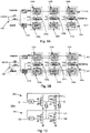
- Figure 8 illustrates the phase relationships between the 40MHz reference clock signal 306, the 40MHz feedback clock signal 308, the 600 MHz signal 317 output by the divide-by-8 divider 316 of the first divider circuitry, and the 600MHz output clock signal 322 output by the second divider circuitry 320.
- Figure 8 shows that the 600MHz output clock signal 322 is in advance of the 40MHz reference clock signal 306 by an adjustable 'skew' amount 400.
- the range 402 of possible 'skew' amounts is from 0 to 15/16 T.
- the divide-by-8 divider 316 Since the divide-by-8 divider 316 is part of the feedback loop of the PLL, the phase relation between the 600MHz signal 317 output by the divide-by-8 divider 316 and the 40MHz feedback clock signal 308 is automatically fixed, that is, their rising edges will always coincide.
- the 600MHz signal 317 output by the divide-by-8 divider 316 in the feedback path is delayed for a part of its period, the 600MHz output clock signal 322 for the ADC 150, 250 becomes advanced with respect to the 40MHz reference clock signal 306, as shown in Figure 8 .
- the rising edge of the 600 MHZ output clock signal 322 in the slave IC can only be advanced with respect to the incoming 40MHz reference clock signal 306.
- the timing of the output clock signal 322 in the master IC 14 can be advanced instead.
- the configuration shown in Figure 7 does not allow the 600MHz output clock signal 322 to be advanced by more than a single period with respect to the incoming 40MHz reference clock signal 306.
- the delay between the respective reference clock signals 306 of the master and slave ICs 14, 16 may be greater than one period of the 600MHz output clock signal 322.
- This 40MHz ADC reference clock signal 326 corresponds to the 'Init' signal 160 indicated in Figures 4 and 6 .
- the 40MHz ADC reference clock signal 326 is output by an ADC reference clock re-clocking unit 328, which re-clocks the 40MHz feedback clock signal 308 based on the 600MHz output clock, i.e. it shifts the 40MHz ADC reference clock signal 326 over a number of periods of the 600MHz output clock signal 322. This enables compensation of any amount of delay, provided it is less than the period of the 40MHz ADC reference clock signal 326.
- Figures 9A and 9B show two embodiments of the two divide-by-8 divider chains 316, 320, shown in Figure 7 .
- the divide-by-8 divider 320 of the second divider circuitry operates as a master divider
- the divide-by-8 divider 316 of the first divider circuitry operates as a slave divider.
- the master divider 320 generates the output clock signal 322 for the ADC150, 250, while the slave divider 316 is part of the feedback loop.
- the divide-by-8 divider 320 of the second divider circuitry 320 is built from three gated divide-by-two master dividers 320a, 320b, 320c.
- the divide-by-8 divider 316 of the first divider circuitry 316, 318 is built from three gated divide-by-two slave dividers 316a, 316b, 316c.
- the first divide-by-two master divider 320a, of the second divider circuitry 322 operates as a master to the first divide-by-two slave divider 316a of the first divider circuitry 316, 318 to form a first master-slave pair 320a, 320b, and so on, giving a second master-slave pair 320b, 316b and a third master-slave pair 320c, 316c of dividers.
- the first master divider 320a receives the oscillator signal output by the level shifter 314 as its clock input ('Mclk').
- An inverter 330 receives the oscillator signal and outputs an inverted oscillator signal.
- a switching device 332 is provided for selecting between the oscillator signal and the inverted oscillator signal.
- the first slave divider 316a is arranged to selectively receive the oscillator signal or the inverted oscillator signal output from the switching device 332 as its clock input ('Sclk'), dependent upon a control signal 'skew0' input to the switching device 332.
- the finest skew step i.e. 1 ⁇ 2 a period of the 4.8 GHz oscillator signal, or 104ps. This corresponds to a shift of 1/16 of a period of the 600MHz output clock signal 322.
- the complete divide-by-8 divider chain three equal divide-by-2 stages are used, in which the master divide-by-2 divider 320a, 320b, 320c generates four phases, and the corresponding slave divider 316a, 316b, 316c re-clocks a selected one of these four phases, selected using a respective multiplexer 334a, 334b, 334c controlled by the control signals 'skew0', 'skew1', 'skew2', 'skew3' (collectively indicated as control signal 324 in Figure 7 ).
- the complete divide-by-8 chain shown in Figure 9 enables the phase of the 600MHz clock signal 317 output by the divide-by-8 divider 316 (i.e. the slave) to be shifted in 1/16 period steps compared with the 600MHz output clock signal 322 output by the divide-by-8 divider 320 (i.e. the master), between 1/16 T and 15/16 T.
- the master divide-by-two dividers 320a, 320b, 320c and the slave divide-by-two dividers 316a, 316b, 316c use the same circuit to guarantee equal delays.
- Each slave divide-by-2 divider 316a, 316b, 316c can be either regarded as a re-clocking circuit or as a gated divider. Functionally seen, it is re-clocking a selected output of the corresponding master divide-by-2 divider 320a, 320b, 320c with the slave clock 'Sclk', but circuit-wise it is exactly the same divider circuit in master as well as slave.
- Figure 9A The embodiment shown in Figures 9A is simpler than that shown in Figure 9B in that it generates single-ended signals.
- Figure 9B uses and generates (semi) differential clk and clkn signals so that opposite clock phases are available without delay.
- Figure 10 illustrates an embodiment of the master divide-by-2 divider 320a in the form of a semi-differential flip-flop with four phase outputs L, Ln, Q, and Qn.
- the slave divide-by-2 divider 316a uses the same circuit.
- the divide-by-2 divider 320a comprises two single-ended flip-flops 340, 342. By using outputs of both latches of the first flip-flop 340, both phases L and Q are available from the first flip-flop.
- the second flip-flop 342 is used to generate the opposite phase output signals, Ln and Qn, with exactly the same delays from clock to output. The correct phase relation between the two flip-flops 340, 342 is obtained by gating.
- the divide-by-2 divider 320a also includes latches between the L and Ln outputs and between the Q and Qn outputs.
- the gate-input G of the first flip-flop 340 is set to 1 and the gate-input Gn of the second flip-flop 342 is connected to the inverted Q output of the first flip-flop 340 in order to align both semi-differential flip-flop halves 340, 342 in opposite phase.
- both the G and Gn gate inputs of the divider 316a are connected to the required signals selected by the multiplexer 334a from the four phase outputs of the master divider 320a based on the control signals 'skew0', 'skew1', 'skew2', 'skew3' determining the skew setting.
- Figure 11 illustrates the master divide-by-2 divider 320a and the slave divide-by-2 divider 316a together with the respective multiplexer 334a.
- the second and third master-slave pairs 320b, 316b and 320c, 316b, use the same circuit.
- the respective multiplexer 334a, 334b, 334c selects the required gating signals for the respective slave divider 316a, 316b, 316c.
- Figure 12 shows an embodiment of the multiplexer 334a, 334b, 334c using pipelining with an additional internal latch stage. This has a selection stage at the input, controlled by control signal 'sel', followed by a clocked latch stage and a further selection stage. This implementation is used to reach the high speed requirement.
- the amount of skew compensation provided by the PLL clock generator 108, 110, 208, 210 is controlled via the control inputs 324, shown as 'skew0'...'skew3' in Figures 9A and 9B .
- the amount of skew compensation required is a function of the length of the PCB transmission lines 124 for transmitting the reference clock signal 106 between the master and slave ICs 14, 16.
- the skew compensation amount may be determined by an initial calibration. If the PCB delay is expected to change, for example due to second-order effects such as temperature changes, then a feed-forward compensation may be applied with a-priori stored coefficients on the central MCU 12. A number of temperature sensors may be provided for this purpose.
Landscapes
- Stabilization Of Oscillater, Synchronisation, Frequency Synthesizers (AREA)
- Manipulation Of Pulses (AREA)
Abstract
Description
- The present invention relates to an apparatus comprising a phase-locked loop. In particular, but not exclusively, it relates to a radar receiver or transceiver.
- High performance automotive radar sensors for autonomous driving need to comply with stringent angular resolution requirements. Angular resolution relates directly to the system total antenna aperture, which in turn normally relates to the number of receive antennas and their localization with respect to each other.
- To avoid so-called grating lobes in the angular response (i.e. false target detection at certain angular positions), it is necessary that the antennas be located not further than λ/2 from each other, with λ being the wavelength of carrier signal. In practice, aperture sizes in the range of 6 λ to 10 A are common, which combined with the λ/2 criteria for each antenna leads to a number of antenna receiver elements between 12 and 20.
-
Figure 1 shows an image of an example radar sensor comprising 12 RX antennas attached to three separate RX chips. A TX chip can be seen on the left part of the image, while the three RX chips can be seen in the central part of the image. Each of the 12 RX antenna elements connects to a separate receiver channel, with the receiver channels being distributed across the three RX chips. - For a complete system realization, each RX antenna signal must be downconverted to baseband and then transferred to the digital domain using a respective analog-to-digital converter (ADC). Both the local oscillator signal used to downconvert the RX antenna signals and the sampling clock signal of the different ADCs must be phase-coherent and stable with respect to the corresponding signals of the other ADCs. Otherwise, errors in the angular position estimates are introduced during signal processing in the base-band, and the advantages of using a large array to increase sensor angular resolution may be lost.
- Several integrated circuit chip-sets are available, offering down-conversion operation and flexibility for creating different sizes of antenna arrays. In addition to the example shown in
Figure 1 , further example configurations of RX and TX channels supported by combinations of available chips are presented inFigure 2 . However these circuits do not offer integrated ADCs and as such do not deal with the requirement for ADC clock synchronization discussed above. - Aspects of the invention are set out in the accompanying claims. Combinations of features from the dependent claims may be combined with features of the independent claims as appropriate and not merely as explicitly set out in the claims.
- According to an aspect of the invention, there is provided an apparatus comprising:
- a first phase-locked loop comprising:
- a phase detector, arranged to receive a reference clock signal and a feedback clock signal and to output a frequency control signal based on a phase difference between the reference clock signal and the feedback clock signal;
- a variable-frequency oscillator arranged to output an oscillator signal having a frequency dependent on said frequency control signal;
- first divider circuitry for generating said feedback clock signal by frequency-dividing said oscillator signal; and
- second divider circuitry for generating an output clock signal by frequency-dividing said oscillator signal;
- wherein a phase relation between said first divider circuitry and said second divider circuitry is adjustable to delay or advance said output clock signal relative to said feedback clock signal.
- By enabling the output clock signal to be delayed or advanced relative to the feedback clock signal, the present invention enables compensation of timing differences due to delays in transmission of a reference clock signal between different elements of the apparatus, thereby improving clock synchronisation. In particular, the present invention enables compensation of timing delays due to PCB skew.
- In some embodiments, the apparatus further comprises an inverter for inverting said oscillator signal to generate an inverted oscillator signal, wherein:
- one of said first divider circuitry and said second divider circuitry comprises a first master divider arranged to receive said oscillator signal;
- the other one of said first divider circuitry and said second divider circuitry comprises a first slave divider arranged to selectively receive said oscillator signal or said inverted oscillator signal; and
- said first slave divider is configured to re-clock a selected output of said first master divider based on said selected one of said oscillator signal and said inverted oscillator signal.
- This enables one of the feedback clock signal or the output clock signal to be delayed by a step of half a period of the oscillator signal.
- The output clock signal may be delayed or advanced relative to said feedback clock signal by a multiple of one half of a period of said oscillator signal.
- Said first master divider and said first slave divider may each be configured to divide by 2.
- In some embodiments, said first slave divider is configured to re-clock a selected one of four-phase outputs of said first master divider.
- In some embodiments, said first slave divider comprises the same circuitry as said first master divider.
- This may help to ensure equal delays at the master and slave dividers.
- In some embodiments, said first master divider comprises a differential or semi-differential flip-flop.
- This may enable outputs of opposite phase to be available without incurring a relative delay.
- In some embodiments:
- said one of said first divider circuitry and said second divider circuitry comprises a second master divider arranged to receive an output of said first master divider;
- said other one of said first divider circuitry and said second divider circuitry comprises a second slave divider arranged to receive an output of said first slave divider; and
- said second slave divider is configured to re-clock a selected output of said second master divider based on said output of said first slave divider.
- In some embodiments:
- said one of said first divider circuitry and said second divider circuitry comprises a third master divider arranged to receive an output of said second master divider;
- said other one of said first divider circuitry and said second divider circuitry comprises a third slave divider arranged to receive an output of said second slave divider; and
- said third slave divider is configured to re-clock a selected output of said third master divider based on said output of said second slave divider.
- Said second master divider and said second slave divider may be each configured to divide by two.
- Said third master divider and said third slave divider may be each configured to divide by two.
- The output clock signal may have a frequency equal to one eighth of the frequency of the oscillator signal.
- Said second divider circuitry may comprise at least one further divider.
- The apparatus may further comprise circuitry for re-clocking said feedback clock signal based on said output clock signal.
- This may enable adjustment of the output clock frequency relative to the feedback clock frequency by more than one period of the output clock frequency.
- The reference clock signal may be received via a printed circuit board.
- In some embodiments, the apparatus comprises:
- a first integrated chip comprising:
- said first phase-locked loop, and
- a first ADC arranged to receive said output clock signal.
- In some embodiments, said apparatus comprises:
- a second integrated chip, comprising:
- a second phase-locked loop configured to output a further output clock signal; and
- a further ADC arranged to receive said further output clock signal;
- wherein said first integrated chip is arranged to receive said reference clock signal from said second integrated chip.
- The first phase-locked loop may comprise circuitry for buffering said reference clock signal.
- The apparatus may be a radar receiver or transceiver.
- In a radar receiver or transceiver, circuitry required for signal generation, transmission and/or reception may also be included in the first and/or second integrated chip.
- The apparatus may be a phased-array radar receiver or transceiver.
- Embodiments of the present invention will be described, by way of example only, with reference to the accompanying drawings in which like reference signs relate to like elements and in which:
-
Figure 1 shows an image of an example radar sensor comprising 12 RX antennas attached to three separate RX chips; -
Figure 2 shows example configurations of RX and TX channels supported by combinations of available chips; -
Figure 3 shows a configuration of a multiple-chip radar sensor system 10 according to an example embodiment of the present invention; -
Figure 4 is a block diagram illustrating one of the receiver (RX) channels of the radar system shown inFigure 3 ; -
Figures 5 illustrates two radar integrated chips (ICs) operating as master IC and slave IC in a multiple IC radar receiver system, according to an example embodiment of the present invention; -
Figures 6A and6B illustrate the internal architecture of the clock circuitry for the master IC and slave IC respectively ofFigure 5 , according to an example embodiment of the present invention; -
Figure 7 illustrates a phase-locked loop (PLL) clock generator for the master and slave ICs ofFigures 6A and6B , according to an example embodiment of the present invention; -
Figure 8 illustrates the phase relationships between various signals generated by the circuitry ofFigure 7 ; -
Figures 9A and 9B illustrate embodiments of a divider chain for the PLL clock generator ofFigure 7 ; -
Figure 10 illustrates a divide-by-2 divider for the divider chain ofFigures 9A and 9B , according to an example embodiment of the present invention; -
Figure 11 illustrates a master-slave pair of divide-by-2 dividers for the divider chain ofFigures 9A and 9B , according to an example embodiment of the present invention; and -
Figure 12 illustrates a multiplexer for the master-slave pair of divide-by-2 dividers ofFigure 11 , according to an example embodiment of the present invention. -
Figure 3 shows a configuration of a multiple-chip radar sensor system 10 according to an embodiment of the present invention. The system 10 comprises a main computing unit (MCU) 12, a "master" integrated chip (IC) 14 and a number of "slave" ICs 16 (of which two are shown inFigure 3 ). - The "master"
IC 14 provides a number of signals to the "slave"ICs 16, including: a local oscillator signal (LO) 20, used for the transmit (TX) amplifiers and receiver (RX) mixers (not shown inFigure 3 ); a "chirp start"signal 22, used to trigger the starting point of the timing engines (not shown inFigure 3 ) within eachIC reference clock signal 24, used as a time base for synchronization of the sampling moments on the ADCs on the master and slave ICs. In the arrangement shown inFigure 3 , themaster IC 14 has a local oscillator (LO) input port ("LO in", 20a) in addition to the local oscillator output port ("LO out", 20b). The use of separate LO input andoutput ports - The
MCU 12 is connected to the master and slave ICs (14, 16) by SPI (serial peripheral interface) control lines (30) and digital lines (32), for example using CSI-2, LVDS or CIF formats, for receiving data from the ICs (14, 16). - In a typical configuration, each IC contains three operational transmit (TX) ports and four receiver (RX) ports. Thus the arrangement shown in
Figure 3 comprising a master IC and two slave ICs would typically offer 9 transmit (TX) ports and 12 receiver (RX) ports in total, althoughFigure 3 shows only one TX and one RX port is shown for each IC. -
Figure 4 is a block diagram illustrating one of the receiver (RX) channels of the radar system shown inFigure 3 . Each RX channel includes the same functional blocks:amplifier 44,mixer 46, intermediate frequency (IF)filter 48,ADC 50,decimation stage 52 andserial interface 54, as is known in the art. The main control and timing signals are: - a local oscillator (LO) signal 56 input to the
mixer 46, - an 'ADC Clock'
signal 58, for determining the sampling moments of the ADC, and an 'Init'signal 60 for theADC 50, and - a 'Valid data'
signal 62 for thedecimation stage 52 andserial interface 54, providing timing information indicating at which moment the ADC data is to be considered as valid radar data. - For optimal operation of the distributed radar system, it is important that these control and timing signals 56, 58, 60, 62 are synchronous across all receiver (RX) channels on
different ICs - For the next generation of highly-integrated radar sensors, in which signal generation, transmission, reception and digitization are integrated in a single monolithic die, a method to synchronize and stabilize the phase of the
ADC clock 58 acrossdifferent ICs - Printed circuit board (PCB) skews on synchronization signals transmitted between
different chips respective ADC 50 to the baseband processor (MCU) 12. More specifically, a shift in the sampling time moment of theADC 50 translates into an equivalent error in the phase of the sampled signal output by theADC 50. The error is proportional to the frequency of signal being sampled, leading to a frequency-dependent phase error component. This is undesirable, for several reasons. - In a phased array receiver, the relative phase of the signals received across several receivers indicates the angular position of a reflecting object with respect to the radar sensor. Therefore, if the accuracy of the received signal phases is compromised due to sampling moment deviations, due for example to a skew on the connecting line between two chips in the phased array receiver, an error is introduced in the estimation of the angular position of the reflecting object with respect to the radar sensor. This is obviously undesirable, as it decreases the angular detection performance of the radar sensor.
- In applications in which two or
more radar ICs IC master IC 14, the other(s) as slave IC(s) 16. -
Figures 5 illustrates tworadar ICs master IC 14 andslave IC 16 in a multiple IC receiver system. Although only oneslave IC 16 is shown, the system may comprisemultiple slave ICs 16. - The
master IC 14 illustrated inFigure 5 includes anamplifier 144, amixer 146 arranged to receive aLO signal 156, an intermediate frequency (IF)filter 148, and anADC 150 arranged to receive anADC clock signal 158, as discussed above. Themaster IC 14 uses acrystal resonator 102 and associatedoscillator circuitry 104 to create the overall system time-base, which is then shared with theslave IC 14. In a typical application, thecrystal oscillator reference clock signal 106. A phase locked loop (PLL) 108, 110 is referenced to thecrystal oscillator ADC clock signal 158 for theADC 150 on theMaster IC 14. - The
slave IC 16 illustrated inFigure 5 also includes anamplifier 244, amixer 246 arranged to receive anLO signal 256, an intermediate frequency (IF)filter 248, and anADC 250 arranged to receive anADC clock signal 258 as discussed above. Thereference clock signal 106 generated by thecrystal oscillator Master IC 14 is transferred to theslave IC 16 via aPCB connection 124 of a printed circuit board (PCB) 18. Theslave IC 16 includesoscillator circuitry 204, which is identical to theoscillator circuitry 104 of themaster IC 16 connected to thecrystal resonator 102, which operates as an input buffer for thereference clock signal 106 received at theslave IC 16 from themaster IC 14. Theslave IC 16 also includes aPLL clock generator ADC 250 on theslave IC 16. - However, the
PCB connection 124 between the master andslave ICs respective ADCs slave ICs ADC 250 of theslave IC 16 to be delayed with respect to the sampling moment of theADC 150 of themaster IC 14, typically by a few nanoseconds. As discussed above, this timing difference leads to an error on the relative phase of the digitized signal produced by the master andslave ADCs - To illustrate the effect of the PCB skew τPCB, the specified phase stability between RX channels usually requires the phase deviation to be contained within +/-2 degrees. For an intermediate frequency (IF) frequency of up to 10 MHz, a realistic yet small PCB skew of ∼1ns leads to a 3.6 degree phase estimation error at the highest IF frequency, due to the shift in sampling moment. For the next generation of radar sensors with IF frequencies of up to 20MHz, the same 1ns PCB skew will result in a 7.2 degree error in the phase estimation, which is much above the overall phase stability specification mentioned above. Therefore, it is necessary that systems with distributed ADCs incorporate means for correcting PCB skews.
- To compensate for the time delay introduced by PCB skew τPCB, the
PLL clock generators Figure 5 includecircuitry respective ADCs slave ICs -
Figures 6A and6B illustrate the internal architecture of the clock circuitry of themaster IC 14 andslave ICs 16 respectively, which include the following elements: - The
oscillator circuitry 104 on themaster IC 14 is attached to acrystal resonator 102. It creates the fundamental time base for the complete distributed system, outputting a (typical) 40 MHz signal 106 that is distributed to theslave ICs 16 via aPCB connection 124. At theslave ICs 16, the 40MHz clock signal 106 is input to theoscillator circuitry 204 by the corresponding port as thecrystal resonator 102 in themaster IC 14. In this way, theoscillator circuitry 204 within theslave ICs 16 operates as a buffer to the externalreference clock signal 106. Note that thereference clock signal 106 arriving at eachslave IC 16 will be delayed by a certain amount of time, depending (among other factors) on the PCB distance between themaster IC 14 and therespective slave IC 16. - The
PLL clock generator reference clock signal 106 as a reference for creating create the high frequencyADC clock signal 158 for theADC 150 in the receiver. The ADC clock signal 158 from thePLL clock generator chirp generator 170. In the case of aslave IC 16, the 40MHz reference clock 106 comes from themaster IC 14 by means of aPCB connection 124, as mentioned above. In this situation, the phase of theADC clock signal 258 will also suffer from a phase difference, with respect to the correspondingADC clock signal 158 generated at themaster IC 14, that is proportional to the PCB distance (also referred to as "PCB skew") distance between themaster IC 14 and therespective slave IC 16. - The
chirp generation circuit 170 creates the LO signal 156 to be used at themaster IC 14 and at theslave ICs 16. At themaster IC 14, the LO signal is output as the 'LO out'signal 120b for distribution to the respective 'LO in'inputs slave ICs master IC 14, a multiplexer (MUX) 172 transfers the LO signal 156 from the 'LO in'input 120a towards themixer 146. A correspondingMUX 272 is provided in the slave IC 16.TheMUX 172 is a support function that allows theMaster IC 14 to transfer the LO signal 156 internally to the RX and TX section, if desired. In the configuration shown inFigures 6A and6B , theMUX internal LO node ICs slave IC 16, the correspondingchirp generation circuit 270 is disabled and the 'LO out'port 220b is not used. - In addition, the master and
slave ICs timing engine signal corresponding decimation stage 52 and serial interface 54 (Figure 4 ) of the corresponding RX channel. Thetiming engine 174 of themaster IC 14 also outputs a 'chirp start'signal 122 for triggering the starting point of thetiming engines IC master IC 14 and theslave IC 16. Eachmaster IC 14 andslave IC 16 includes anSPI bus MCU 12. -
Figure 7 illustrates thePLL clock generator slave ICs phase detector frequency detector 302 andcharge pump 304, is arranged to receive thereference clock signal 306 and afeedback clock signal 308. In the case of themaster IC 14, thereference clock signal 306 is thereference clock signal 106 output by thecrystal oscillator slave IC 16, thereference clock signal 306 is clock signal 206 output by the oscillator circuitry 206 which receives and buffers thereference clock signal 106 received from themaster IC 14 via thePCB connection 124. In this embodiment, thereference clock signal 306 is a 40MHz clock signal. The output of thephase detector low pass filter 310 to provide a frequency control signal based on a phase difference between thereference clock signal 306 and thefeedback clock signal 308. A variable-frequency oscillator, in the form of a VCO (voltage controlled oscillator) 312 controlled by the frequency control signal, outputs an oscillator signal having a frequency dependent on the frequency control signal. The oscillator signal is level shifted by a level shifter (LS) 314. In this embodiment, the oscillator signal has a frequency of 4.8 GHz. - The level-shifted oscillator signal is input into
first divider circuitry feedback clock signal 308, in this case a 40MHz feedback clock signal, by frequency dividing the oscillator signal. In this embodiment, thefirst divider circuitry cascaded divider 316, and a divide-by-15cascaded divider 318. The level-shifted oscillator signal is also input intosecond divider circuitry 320 for generating anoutput clock signal 322, in this embodiment a 600MHzoutput clock signal 322 for clocking theADC respective IC second divider circuitry 320 is in the form of a divider chain comprising a divide-by-8cascaded divider 320. The 600 MHZoutput clock signal 322 corresponds to the respectiveADC clock signal 158, 258 (Figures 4 ,5 and6 ) in themaster IC 14 andslave IC 14. - The divide-by-8
divider 316 of thefirst divider circuitry 316, 318 (i.e. the divide-by 8 divider in the feedback loop of the PLL) is synchronized to the divide-by-8divider 320 of the second divider circuitry since each one receives the level-shifted oscillator signal generated by theVCO 312 as its clock input. Importantly, the exact phase relation between the divide-by-8divider 316 of the first divider circuitry and the divide-by-8divider 320 of the second divider circuitry is adjustable to delay thefeedback clock signal 308 relative to theoutput clock signal 322, by means ofcontrol inputs 324. Equivalently, this has the effect of advancing theoutput clock signal 322 relative to thefeedback clock signal 308. - The skilled person will appreciate that further divide or multiply stages may be included between the output of the
VCO 312 and the first andsecond divider circuitry -
Figure 8 illustrates the phase relationships between the 40MHzreference clock signal 306, the 40MHzfeedback clock signal 308, the 600 MHz signal 317 output by the divide-by-8divider 316 of the first divider circuitry, and the 600MHzoutput clock signal 322 output by thesecond divider circuitry 320.Figure 8 shows that the 600MHzoutput clock signal 322 is in advance of the 40MHzreference clock signal 306 by an adjustable 'skew'amount 400. Therange 402 of possible 'skew' amounts is from 0 to 15/16 T. - The phase of the 600MHz signal 317 output by the divide-by-8
divider 316 of the first divider circuitry (in the feedback loop) can be delayed (relative to the 600MHzoutput clock signal 322 output by the divide-by-8divider 320 of the second divider circuitry) from 0 to 15/16 of the time period T, where T=1/(600MHz), in steps of (1/16)T, which corresponds to approximately 104ps. - Since the divide-by-8
divider 316 is part of the feedback loop of the PLL, the phase relation between the 600MHz signal 317 output by the divide-by-8divider 316 and the 40MHzfeedback clock signal 308 is automatically fixed, that is, their rising edges will always coincide. When, as described above, the 600MHz signal 317 output by the divide-by-8divider 316 in the feedback path is delayed for a part of its period, the 600MHzoutput clock signal 322 for theADC reference clock signal 306, as shown inFigure 8 . - Using this arrangement for the
PLL clock generator slave IC 16, the rising edge of the 600 MHZoutput clock signal 322 in the slave IC can only be advanced with respect to the incoming 40MHzreference clock signal 306. When, at theslave IC 16, a delay of the 600MHzoutput clock signal 322 would be desired, the timing of theoutput clock signal 322 in themaster IC 14 can be advanced instead. - The configuration shown in
Figure 7 does not allow the 600MHzoutput clock signal 322 to be advanced by more than a single period with respect to the incoming 40MHzreference clock signal 306. However, the delay between the respective reference clock signals 306 of the master andslave ICs output clock signal 322. To accommodate greater delays, it is possible to manipulate a 40MHz ADCreference clock signal 326, which goes to therespective ADC reference clock signal 326 corresponds to the 'Init'signal 160 indicated inFigures 4 and6 . The 40MHz ADCreference clock signal 326 is output by an ADC referenceclock re-clocking unit 328, which re-clocks the 40MHzfeedback clock signal 308 based on the 600MHz output clock, i.e. it shifts the 40MHz ADCreference clock signal 326 over a number of periods of the 600MHzoutput clock signal 322. This enables compensation of any amount of delay, provided it is less than the period of the 40MHz ADCreference clock signal 326. -
Figures 9A and 9B show two embodiments of the two divide-by-8divider chains Figure 7 . To obtain the skewing function (i.e. the time delay/advance between the two divide-by-8dividers 316, 320), the divide-by-8divider 320 of the second divider circuitry operates as a master divider, while the divide-by-8divider 316 of the first divider circuitry (in the feedback loop) operates as a slave divider. This enables control of the phase relation between the outputs of themaster divider 320 andslave divider 316. Themaster divider 320 generates theoutput clock signal 322 for the ADC150, 250, while theslave divider 316 is part of the feedback loop. - In both embodiments (
Figures 9A and 9B ), the divide-by-8divider 320 of thesecond divider circuitry 320 is built from three gated divide-by-twomaster dividers divider 316 of thefirst divider circuitry slave dividers master divider 320a, of thesecond divider circuitry 322 operates as a master to the first divide-by-twoslave divider 316a of thefirst divider circuitry slave pair slave pair slave pair - The
first master divider 320a receives the oscillator signal output by thelevel shifter 314 as its clock input ('Mclk'). Aninverter 330 receives the oscillator signal and outputs an inverted oscillator signal. A switching device 332 is provided for selecting between the oscillator signal and the inverted oscillator signal. Thefirst slave divider 316a is arranged to selectively receive the oscillator signal or the inverted oscillator signal output from the switching device 332 as its clock input ('Sclk'), dependent upon a control signal 'skew0' input to the switching device 332. By switching the clock input of the first divide-by-2slave divider 316a between the normal and inverted phase of the oscillator signal, it is possible to obtain the finest skew step, i.e. ½ a period of the 4.8 GHz oscillator signal, or 104ps. This corresponds to a shift of 1/16 of a period of the 600MHzoutput clock signal 322. - In the complete divide-by-8 divider chain, three equal divide-by-2 stages are used, in which the master divide-by-2
divider corresponding slave divider respective multiplexer control signal 324 inFigure 7 ). The complete divide-by-8 chain shown inFigure 9 enables the phase of the600MHz clock signal 317 output by the divide-by-8 divider 316 (i.e. the slave) to be shifted in 1/16 period steps compared with the 600MHzoutput clock signal 322 output by the divide-by-8 divider 320 (i.e. the master), between 1/16 T and 15/16 T. - The master divide-by-two
dividers dividers divider divider - The embodiment shown in
Figures 9A is simpler than that shown inFigure 9B in that it generates single-ended signals. In contrast,Figure 9B uses and generates (semi) differential clk and clkn signals so that opposite clock phases are available without delay. -
Figure 10 illustrates an embodiment of the master divide-by-2divider 320a in the form of a semi-differential flip-flop with four phase outputs L, Ln, Q, and Qn. The slave divide-by-2divider 316a uses the same circuit. The divide-by-2divider 320a comprises two single-ended flip-flops flop 340, both phases L and Q are available from the first flip-flop. The second flip-flop 342 is used to generate the opposite phase output signals, Ln and Qn, with exactly the same delays from clock to output. The correct phase relation between the two flip-flops divider 320a also includes latches between the L and Ln outputs and between the Q and Qn outputs. - When used as the master divide-by-2
divider 320a, the gate-input G of the first flip-flop 340 is set to 1 and the gate-input Gn of the second flip-flop 342 is connected to the inverted Q output of the first flip-flop 340 in order to align both semi-differential flip-flop halves divider 316a, both the G and Gn gate inputs of thedivider 316a are connected to the required signals selected by themultiplexer 334a from the four phase outputs of themaster divider 320a based on the control signals 'skew0', 'skew1', 'skew2', 'skew3' determining the skew setting. -
Figure 11 illustrates the master divide-by-2divider 320a and the slave divide-by-2divider 316a together with therespective multiplexer 334a. The second and third master-slave pairs respective multiplexer respective slave divider Figure 12 shows an embodiment of the multiplexer 334a, 334b, 334c using pipelining with an additional internal latch stage. This has a selection stage at the input, controlled by control signal 'sel', followed by a clocked latch stage and a further selection stage. This implementation is used to reach the high speed requirement. - As mentioned above, the amount of skew compensation provided by the
PLL clock generator control inputs 324, shown as 'skew0'...'skew3' inFigures 9A and 9B . The amount of skew compensation required is a function of the length of thePCB transmission lines 124 for transmitting thereference clock signal 106 between the master andslave ICs central MCU 12. A number of temperature sensors may be provided for this purpose. - Although particular embodiments of the invention have been described above, it will be appreciated than many modifications, including additions and/or substitutions, may be made within the scope of the appended claims.
Claims (15)
- An apparatus comprising:a first phase-locked loop comprising:a phase detector, arranged to receive a reference clock signal and a feedback clock signal and to output a frequency control signal based on a phase difference between the reference clock signal and the feedback clock signal;a variable-frequency oscillator arranged to output an oscillator signal having a frequency dependent on said frequency control signal;first divider circuitry for generating said feedback clock signal by frequency-dividing said oscillator signal; andsecond divider circuitry for generating an output clock signal by frequency-dividing said oscillator signal;wherein a phase relation between said first divider circuitry and said second divider circuitry is adjustable to delay or advance said output clock signal relative to said feedback clock signal.
- An apparatus according to claim 1, further comprising an inverter for inverting said oscillator signal to generate an inverted oscillator signal, wherein:one of said first divider circuitry and said second divider circuitry comprises a first master divider arranged to receive said oscillator signal;the other one of said first divider circuitry and said second divider circuitry comprises a first slave divider arranged to selectively receive said oscillator signal or said inverted oscillator signal; andsaid first slave divider is configured to re-clock a selected output of said first master divider based on said selected one of said oscillator signal and said inverted oscillator signal.
- An apparatus according to claim 1 or claim 2, wherein said output clock signal is delayed or advanced relative to said feedback clock signal by a multiple of one half of a period of said oscillator signal.
- An apparatus according to claim 2 or claim 3, wherein said first master divider and said first slave divider are each configured to divide by 2.
- An apparatus according to any one of claims 2 to 4, wherein said first slave divider is configured to re-clock a selected one of four phase outputs of said first master divider.
- An apparatus according to any one of claims 2 to 5, wherein said first slave divider comprises the same circuitry as said first master divider.
- An apparatus according to any one of claims 2 to 6, wherein said first master divider comprises a differential flip-flop.
- An apparatus according to any one of claims 2 to 7, wherein:said one of said first divider circuitry and said second divider circuitry comprises a second master divider arranged to receive an output of said first master divider;said other one of said first divider circuitry and said second divider circuitry comprises a second slave divider arranged to receive an output of said first slave divider; andsaid second slave divider is configured to re-clock a selected output of said second master divider based on said output of said first slave divider.
- An apparatus according to claim 8, wherein:said one of said first divider circuitry and said second divider circuitry comprises a third master divider arranged to receive an output of said second master divider;said other one of said first divider circuitry and said second divider circuitry comprises a third slave divider arranged to receive an output of said second slave divider; andsaid third slave divider is configured to re-clock a selected output of said third master divider based on said output of said second slave divider.
- An apparatus according to any one of claims 1 to 8, wherein said second divider circuitry comprises at least one further divider.
- An apparatus according to any one of claims 1 to 10, further comprising circuitry for re-clocking said feedback clock signal based on said output clock signal.
- An apparatus according to any one of claims 1 to 11, wherein said reference clock signal is received via a printed circuit board.
- An apparatus according to any one of claims 1 to 12, wherein said apparatus comprises:a first integrated chip comprising:said first phase-locked loop; anda first ADC arranged to receive said output clock signal.
- An apparatus according to claim 13, wherein said apparatus comprises:a second integrated chip, comprising:a second phase-locked loop configured to output a further output clock signal; anda further ADC arranged to receive said further output clock signal;wherein said first integrated chip is arranged to receive said reference clock signal from said second integrated chip.
- An apparatus according to any one of claims 1 to 14, wherein said apparatus is a radar receiver or transceiver.
Priority Applications (3)
| Application Number | Priority Date | Filing Date | Title |
|---|---|---|---|
| EP17199331.4A EP3477864B1 (en) | 2017-10-31 | 2017-10-31 | Apparatus comprising a phase-locked loop |
| US16/118,974 US10594327B2 (en) | 2017-10-31 | 2018-08-31 | Apparatus comprising a phase-locked loop |
| CN201811292309.7A CN109728806B (en) | 2017-10-31 | 2018-10-31 | Apparatus comprising a phase locked loop |
Applications Claiming Priority (1)
| Application Number | Priority Date | Filing Date | Title |
|---|---|---|---|
| EP17199331.4A EP3477864B1 (en) | 2017-10-31 | 2017-10-31 | Apparatus comprising a phase-locked loop |
Publications (2)
| Publication Number | Publication Date |
|---|---|
| EP3477864A1 true EP3477864A1 (en) | 2019-05-01 |
| EP3477864B1 EP3477864B1 (en) | 2020-07-08 |
Family
ID=60320627
Family Applications (1)
| Application Number | Title | Priority Date | Filing Date |
|---|---|---|---|
| EP17199331.4A Active EP3477864B1 (en) | 2017-10-31 | 2017-10-31 | Apparatus comprising a phase-locked loop |
Country Status (3)
| Country | Link |
|---|---|
| US (1) | US10594327B2 (en) |
| EP (1) | EP3477864B1 (en) |
| CN (1) | CN109728806B (en) |
Families Citing this family (9)
| Publication number | Priority date | Publication date | Assignee | Title |
|---|---|---|---|---|
| DE102019115107B3 (en) * | 2019-06-05 | 2020-09-24 | Infineon Technologies Ag | RADAR SYSTEM WITH MULTIPLE RADAR CHIPS |
| CN112087224B (en) * | 2019-06-14 | 2025-12-30 | 中兴通讯股份有限公司 | Time synchronization allocation input interface circuit and its delay compensation method |
| CN112311390B (en) * | 2019-07-29 | 2024-05-24 | 瑞昱半导体股份有限公司 | Phase-locked loop circuit |
| US11196454B2 (en) * | 2019-10-09 | 2021-12-07 | Beijing Boe Technology Development Co., Ltd. | Digital transceiver driven by synchronous spread spectrum clock signal for data transmission |
| US11675047B2 (en) * | 2020-09-03 | 2023-06-13 | Nxp B.V. | System and method for local oscillator drift estimation and compensation in cascaded sensors |
| EP4089435B1 (en) | 2021-05-12 | 2025-05-28 | Nxp B.V. | Radar system |
| CN113381755B (en) * | 2021-05-13 | 2022-11-01 | 中电科思仪科技股份有限公司 | Clock system with synchronization function and synchronization realization method thereof |
| EP4375790A1 (en) * | 2022-11-25 | 2024-05-29 | LX Semicon Co., Ltd. | Device and method for multi-chip clock synchronization |
| CN116827335B (en) * | 2023-08-25 | 2023-10-27 | 牛芯半导体(深圳)有限公司 | Frequency divider and data processing circuit |
Citations (1)
| Publication number | Priority date | Publication date | Assignee | Title |
|---|---|---|---|---|
| US20030189464A1 (en) * | 2002-04-04 | 2003-10-09 | Oleg Drapkin | Spurious-free fractional-n frequency synthesizer with multi-phase network circuit |
Family Cites Families (20)
| Publication number | Priority date | Publication date | Assignee | Title |
|---|---|---|---|---|
| US5742208A (en) * | 1996-09-06 | 1998-04-21 | Tektronix, Inc. | Signal generator for generating a jitter/wander output |
| KR100214559B1 (en) * | 1997-02-20 | 1999-08-02 | 구본준 | Frequency doubling |
| EP1213840A1 (en) * | 2000-12-07 | 2002-06-12 | Nokia Corporation | Radio transceiver having a phase-locked loop circuit |
| EP1333581B1 (en) * | 2002-01-30 | 2015-04-08 | Infineon Technologies AG | Clock signal generator |
| US6774689B1 (en) * | 2002-05-23 | 2004-08-10 | Cypress Semiconductor Corp. | Triple input phase detector and methodology for setting delay between two sets of phase outputs |
| US7158603B2 (en) * | 2002-12-26 | 2007-01-02 | Freescale Semiconductor, Inc. | Method and apparatus for compensating deviation variances in a 2-level FSK FM transmitter |
| US7212050B2 (en) * | 2004-12-17 | 2007-05-01 | Seiko Epson Corporation | System and method for synthesizing a clock at digital wrapper (FEC) and base frequencies using one precision resonator |
| US20070127930A1 (en) * | 2005-12-06 | 2007-06-07 | Applied Materials, Inc. | Skew correction system eliminating phase ambiguity by using reference multiplication |
| US7664196B2 (en) * | 2006-11-08 | 2010-02-16 | Raytheon Company | Frequency agile phase locked loop |
| US7504893B2 (en) * | 2006-11-30 | 2009-03-17 | Motorola, Inc. | System and method for reducing transient responses in a phase lock loop with variable oscillator gain |
| US8045670B2 (en) * | 2007-06-22 | 2011-10-25 | Texas Instruments Incorporated | Interpolative all-digital phase locked loop |
| CN104350681A (en) * | 2012-04-12 | 2015-02-11 | 马维尔国际贸易有限公司 | Method and apparatus for local oscillator |
| US9276622B2 (en) * | 2013-03-14 | 2016-03-01 | Qualcomm Incorporated | Local oscillator (LO) generator with multi-phase divider and phase locked loop |
| US9240794B2 (en) * | 2014-01-31 | 2016-01-19 | Silicon Laboratories, Inc | Apparatus and methods for phase-locked loop startup operation |
| US9240795B2 (en) * | 2014-01-31 | 2016-01-19 | Silicon Laboratories, Inc. | Apparatus and methods for phase-locked loop oscillator calibration and lock detection |
| US9325332B2 (en) * | 2014-08-27 | 2016-04-26 | International Business Machines Corporation | Adjusting the magnitude of a capacitance of a digitally controlled circuit |
| US9590644B2 (en) * | 2015-02-06 | 2017-03-07 | Silicon Laboratories Inc. | Managing spurs in a radio frequency circuit |
| EP3276832B1 (en) * | 2015-04-15 | 2019-03-13 | Mitsubishi Electric Corporation | Synthesizer |
| EP3217558B1 (en) * | 2016-03-11 | 2020-05-13 | Socionext Inc. | Timing-difference measurement |
| US9941890B2 (en) * | 2016-06-20 | 2018-04-10 | Altera Corporation | Phase-locked loops with electrical overstress protection circuitry |
-
2017
- 2017-10-31 EP EP17199331.4A patent/EP3477864B1/en active Active
-
2018
- 2018-08-31 US US16/118,974 patent/US10594327B2/en active Active
- 2018-10-31 CN CN201811292309.7A patent/CN109728806B/en active Active
Patent Citations (1)
| Publication number | Priority date | Publication date | Assignee | Title |
|---|---|---|---|---|
| US20030189464A1 (en) * | 2002-04-04 | 2003-10-09 | Oleg Drapkin | Spurious-free fractional-n frequency synthesizer with multi-phase network circuit |
Also Published As
| Publication number | Publication date |
|---|---|
| US20190131981A1 (en) | 2019-05-02 |
| CN109728806B (en) | 2024-03-05 |
| US10594327B2 (en) | 2020-03-17 |
| CN109728806A (en) | 2019-05-07 |
| EP3477864B1 (en) | 2020-07-08 |
Similar Documents
| Publication | Publication Date | Title |
|---|---|---|
| US10594327B2 (en) | Apparatus comprising a phase-locked loop | |
| EP3591434B1 (en) | Communication unit, integrated circuits and method for clock and data synchronization | |
| EP3611540B1 (en) | Apparatus and methods for synchronization of radar chips | |
| US10651859B2 (en) | Radar device, radar system and method for generating a sampling clock signal | |
| EP3591433B1 (en) | Communication unit, integrated circuits and method for clock and data synchronization | |
| US10890654B2 (en) | Radar system comprising coupling device | |
| EP3591435B1 (en) | Communication unit, integrated circuit and method for clock distribution and synchronization | |
| CN110673124B (en) | Communication unit and method for clock distribution and synchronization | |
| US11668793B2 (en) | Radar system | |
| CN114137479B (en) | Local Oscillator Drift Estimation and Compensation System and Method in Cascaded Sensors | |
| US20100080210A1 (en) | System clock synchronization apparatus and method for mobile communication system | |
| JP7493915B2 (en) | Multi-chip timing alignment to a common reference signal | |
| US20040146071A1 (en) | Method and system for clock synchronization of semiconductor devices | |
| JP7488104B2 (en) | Timing Synchronization Circuit | |
| KR101710825B1 (en) | Synchronous data system and method for providing phase-aligned output data | |
| Stackler et al. | A novel method to synchronize high-speed data converters | |
| EP4060664A1 (en) | Minimum intrinsic timing utilization auto alignment on multi-die system | |
| US10659059B2 (en) | Multi-phase clock generation circuit | |
| JP7652020B2 (en) | COMMUNICATION DEVICE, COMMUNICATION METHOD, AND PROGRAM | |
| JPH07200094A (en) | Phase synchronization clock distribution circuit |
Legal Events
| Date | Code | Title | Description |
|---|---|---|---|
| PUAI | Public reference made under article 153(3) epc to a published international application that has entered the european phase |
Free format text: ORIGINAL CODE: 0009012 |
|
| STAA | Information on the status of an ep patent application or granted ep patent |
Free format text: STATUS: THE APPLICATION HAS BEEN PUBLISHED |
|
| AK | Designated contracting states |
Kind code of ref document: A1 Designated state(s): AL AT BE BG CH CY CZ DE DK EE ES FI FR GB GR HR HU IE IS IT LI LT LU LV MC MK MT NL NO PL PT RO RS SE SI SK SM TR |
|
| AX | Request for extension of the european patent |
Extension state: BA ME |
|
| STAA | Information on the status of an ep patent application or granted ep patent |
Free format text: STATUS: REQUEST FOR EXAMINATION WAS MADE |
|
| 17P | Request for examination filed |
Effective date: 20191104 |
|
| RBV | Designated contracting states (corrected) |
Designated state(s): AL AT BE BG CH CY CZ DE DK EE ES FI FR GB GR HR HU IE IS IT LI LT LU LV MC MK MT NL NO PL PT RO RS SE SI SK SM TR |
|
| RIC1 | Information provided on ipc code assigned before grant |
Ipc: H03L 7/18 20060101AFI20191128BHEP |
|
| GRAP | Despatch of communication of intention to grant a patent |
Free format text: ORIGINAL CODE: EPIDOSNIGR1 |
|
| STAA | Information on the status of an ep patent application or granted ep patent |
Free format text: STATUS: GRANT OF PATENT IS INTENDED |
|
| INTG | Intention to grant announced |
Effective date: 20200210 |
|
| GRAJ | Information related to disapproval of communication of intention to grant by the applicant or resumption of examination proceedings by the epo deleted |
Free format text: ORIGINAL CODE: EPIDOSDIGR1 |
|
| STAA | Information on the status of an ep patent application or granted ep patent |
Free format text: STATUS: REQUEST FOR EXAMINATION WAS MADE |
|
| GRAP | Despatch of communication of intention to grant a patent |
Free format text: ORIGINAL CODE: EPIDOSNIGR1 |
|
| STAA | Information on the status of an ep patent application or granted ep patent |
Free format text: STATUS: GRANT OF PATENT IS INTENDED |
|
| INTC | Intention to grant announced (deleted) | ||
| GRAS | Grant fee paid |
Free format text: ORIGINAL CODE: EPIDOSNIGR3 |
|
| GRAA | (expected) grant |
Free format text: ORIGINAL CODE: 0009210 |
|
| STAA | Information on the status of an ep patent application or granted ep patent |
Free format text: STATUS: THE PATENT HAS BEEN GRANTED |
|
| INTG | Intention to grant announced |
Effective date: 20200518 |
|
| AK | Designated contracting states |
Kind code of ref document: B1 Designated state(s): AL AT BE BG CH CY CZ DE DK EE ES FI FR GB GR HR HU IE IS IT LI LT LU LV MC MK MT NL NO PL PT RO RS SE SI SK SM TR |
|
| REG | Reference to a national code |
Ref country code: CH Ref legal event code: EP Ref country code: AT Ref legal event code: REF Ref document number: 1289579 Country of ref document: AT Kind code of ref document: T Effective date: 20200715 |
|
| REG | Reference to a national code |
Ref country code: DE Ref legal event code: R096 Ref document number: 602017019292 Country of ref document: DE |
|
| REG | Reference to a national code |
Ref country code: IE Ref legal event code: FG4D |
|
| REG | Reference to a national code |
Ref country code: LT Ref legal event code: MG4D |
|
| REG | Reference to a national code |
Ref country code: AT Ref legal event code: MK05 Ref document number: 1289579 Country of ref document: AT Kind code of ref document: T Effective date: 20200708 |
|
| REG | Reference to a national code |
Ref country code: NL Ref legal event code: MP Effective date: 20200708 |
|
| PG25 | Lapsed in a contracting state [announced via postgrant information from national office to epo] |
Ref country code: FI Free format text: LAPSE BECAUSE OF FAILURE TO SUBMIT A TRANSLATION OF THE DESCRIPTION OR TO PAY THE FEE WITHIN THE PRESCRIBED TIME-LIMIT Effective date: 20200708 Ref country code: SE Free format text: LAPSE BECAUSE OF FAILURE TO SUBMIT A TRANSLATION OF THE DESCRIPTION OR TO PAY THE FEE WITHIN THE PRESCRIBED TIME-LIMIT Effective date: 20200708 Ref country code: BG Free format text: LAPSE BECAUSE OF FAILURE TO SUBMIT A TRANSLATION OF THE DESCRIPTION OR TO PAY THE FEE WITHIN THE PRESCRIBED TIME-LIMIT Effective date: 20201008 Ref country code: NO Free format text: LAPSE BECAUSE OF FAILURE TO SUBMIT A TRANSLATION OF THE DESCRIPTION OR TO PAY THE FEE WITHIN THE PRESCRIBED TIME-LIMIT Effective date: 20201008 Ref country code: GR Free format text: LAPSE BECAUSE OF FAILURE TO SUBMIT A TRANSLATION OF THE DESCRIPTION OR TO PAY THE FEE WITHIN THE PRESCRIBED TIME-LIMIT Effective date: 20201009 Ref country code: HR Free format text: LAPSE BECAUSE OF FAILURE TO SUBMIT A TRANSLATION OF THE DESCRIPTION OR TO PAY THE FEE WITHIN THE PRESCRIBED TIME-LIMIT Effective date: 20200708 Ref country code: AT Free format text: LAPSE BECAUSE OF FAILURE TO SUBMIT A TRANSLATION OF THE DESCRIPTION OR TO PAY THE FEE WITHIN THE PRESCRIBED TIME-LIMIT Effective date: 20200708 Ref country code: LT Free format text: LAPSE BECAUSE OF FAILURE TO SUBMIT A TRANSLATION OF THE DESCRIPTION OR TO PAY THE FEE WITHIN THE PRESCRIBED TIME-LIMIT Effective date: 20200708 Ref country code: ES Free format text: LAPSE BECAUSE OF FAILURE TO SUBMIT A TRANSLATION OF THE DESCRIPTION OR TO PAY THE FEE WITHIN THE PRESCRIBED TIME-LIMIT Effective date: 20200708 Ref country code: PT Free format text: LAPSE BECAUSE OF FAILURE TO SUBMIT A TRANSLATION OF THE DESCRIPTION OR TO PAY THE FEE WITHIN THE PRESCRIBED TIME-LIMIT Effective date: 20201109 |
|
| PG25 | Lapsed in a contracting state [announced via postgrant information from national office to epo] |
Ref country code: PL Free format text: LAPSE BECAUSE OF FAILURE TO SUBMIT A TRANSLATION OF THE DESCRIPTION OR TO PAY THE FEE WITHIN THE PRESCRIBED TIME-LIMIT Effective date: 20200708 Ref country code: LV Free format text: LAPSE BECAUSE OF FAILURE TO SUBMIT A TRANSLATION OF THE DESCRIPTION OR TO PAY THE FEE WITHIN THE PRESCRIBED TIME-LIMIT Effective date: 20200708 Ref country code: RS Free format text: LAPSE BECAUSE OF FAILURE TO SUBMIT A TRANSLATION OF THE DESCRIPTION OR TO PAY THE FEE WITHIN THE PRESCRIBED TIME-LIMIT Effective date: 20200708 Ref country code: IS Free format text: LAPSE BECAUSE OF FAILURE TO SUBMIT A TRANSLATION OF THE DESCRIPTION OR TO PAY THE FEE WITHIN THE PRESCRIBED TIME-LIMIT Effective date: 20201108 |
|
| PG25 | Lapsed in a contracting state [announced via postgrant information from national office to epo] |
Ref country code: NL Free format text: LAPSE BECAUSE OF FAILURE TO SUBMIT A TRANSLATION OF THE DESCRIPTION OR TO PAY THE FEE WITHIN THE PRESCRIBED TIME-LIMIT Effective date: 20200708 |
|
| REG | Reference to a national code |
Ref country code: DE Ref legal event code: R097 Ref document number: 602017019292 Country of ref document: DE |
|
| PG25 | Lapsed in a contracting state [announced via postgrant information from national office to epo] |
Ref country code: EE Free format text: LAPSE BECAUSE OF FAILURE TO SUBMIT A TRANSLATION OF THE DESCRIPTION OR TO PAY THE FEE WITHIN THE PRESCRIBED TIME-LIMIT Effective date: 20200708 Ref country code: IT Free format text: LAPSE BECAUSE OF FAILURE TO SUBMIT A TRANSLATION OF THE DESCRIPTION OR TO PAY THE FEE WITHIN THE PRESCRIBED TIME-LIMIT Effective date: 20200708 Ref country code: SM Free format text: LAPSE BECAUSE OF FAILURE TO SUBMIT A TRANSLATION OF THE DESCRIPTION OR TO PAY THE FEE WITHIN THE PRESCRIBED TIME-LIMIT Effective date: 20200708 Ref country code: RO Free format text: LAPSE BECAUSE OF FAILURE TO SUBMIT A TRANSLATION OF THE DESCRIPTION OR TO PAY THE FEE WITHIN THE PRESCRIBED TIME-LIMIT Effective date: 20200708 Ref country code: CZ Free format text: LAPSE BECAUSE OF FAILURE TO SUBMIT A TRANSLATION OF THE DESCRIPTION OR TO PAY THE FEE WITHIN THE PRESCRIBED TIME-LIMIT Effective date: 20200708 Ref country code: DK Free format text: LAPSE BECAUSE OF FAILURE TO SUBMIT A TRANSLATION OF THE DESCRIPTION OR TO PAY THE FEE WITHIN THE PRESCRIBED TIME-LIMIT Effective date: 20200708 |
|
| PLBE | No opposition filed within time limit |
Free format text: ORIGINAL CODE: 0009261 |
|
| STAA | Information on the status of an ep patent application or granted ep patent |
Free format text: STATUS: NO OPPOSITION FILED WITHIN TIME LIMIT |
|
| PG25 | Lapsed in a contracting state [announced via postgrant information from national office to epo] |
Ref country code: AL Free format text: LAPSE BECAUSE OF FAILURE TO SUBMIT A TRANSLATION OF THE DESCRIPTION OR TO PAY THE FEE WITHIN THE PRESCRIBED TIME-LIMIT Effective date: 20200708 |
|
| REG | Reference to a national code |
Ref country code: CH Ref legal event code: PL |
|
| 26N | No opposition filed |
Effective date: 20210409 |
|
| PG25 | Lapsed in a contracting state [announced via postgrant information from national office to epo] |
Ref country code: MC Free format text: LAPSE BECAUSE OF FAILURE TO SUBMIT A TRANSLATION OF THE DESCRIPTION OR TO PAY THE FEE WITHIN THE PRESCRIBED TIME-LIMIT Effective date: 20200708 Ref country code: LU Free format text: LAPSE BECAUSE OF NON-PAYMENT OF DUE FEES Effective date: 20201031 Ref country code: SK Free format text: LAPSE BECAUSE OF FAILURE TO SUBMIT A TRANSLATION OF THE DESCRIPTION OR TO PAY THE FEE WITHIN THE PRESCRIBED TIME-LIMIT Effective date: 20200708 |
|
| REG | Reference to a national code |
Ref country code: BE Ref legal event code: MM Effective date: 20201031 |
|
| PG25 | Lapsed in a contracting state [announced via postgrant information from national office to epo] |
Ref country code: LI Free format text: LAPSE BECAUSE OF NON-PAYMENT OF DUE FEES Effective date: 20201031 Ref country code: SI Free format text: LAPSE BECAUSE OF FAILURE TO SUBMIT A TRANSLATION OF THE DESCRIPTION OR TO PAY THE FEE WITHIN THE PRESCRIBED TIME-LIMIT Effective date: 20200708 Ref country code: BE Free format text: LAPSE BECAUSE OF NON-PAYMENT OF DUE FEES Effective date: 20201031 Ref country code: CH Free format text: LAPSE BECAUSE OF NON-PAYMENT OF DUE FEES Effective date: 20201031 |
|
| PG25 | Lapsed in a contracting state [announced via postgrant information from national office to epo] |
Ref country code: IE Free format text: LAPSE BECAUSE OF NON-PAYMENT OF DUE FEES Effective date: 20201031 |
|
| PG25 | Lapsed in a contracting state [announced via postgrant information from national office to epo] |
Ref country code: TR Free format text: LAPSE BECAUSE OF FAILURE TO SUBMIT A TRANSLATION OF THE DESCRIPTION OR TO PAY THE FEE WITHIN THE PRESCRIBED TIME-LIMIT Effective date: 20200708 Ref country code: MT Free format text: LAPSE BECAUSE OF FAILURE TO SUBMIT A TRANSLATION OF THE DESCRIPTION OR TO PAY THE FEE WITHIN THE PRESCRIBED TIME-LIMIT Effective date: 20200708 Ref country code: CY Free format text: LAPSE BECAUSE OF FAILURE TO SUBMIT A TRANSLATION OF THE DESCRIPTION OR TO PAY THE FEE WITHIN THE PRESCRIBED TIME-LIMIT Effective date: 20200708 |
|
| GBPC | Gb: european patent ceased through non-payment of renewal fee |
Effective date: 20211031 |
|
| PG25 | Lapsed in a contracting state [announced via postgrant information from national office to epo] |
Ref country code: MK Free format text: LAPSE BECAUSE OF FAILURE TO SUBMIT A TRANSLATION OF THE DESCRIPTION OR TO PAY THE FEE WITHIN THE PRESCRIBED TIME-LIMIT Effective date: 20200708 |
|
| PG25 | Lapsed in a contracting state [announced via postgrant information from national office to epo] |
Ref country code: GB Free format text: LAPSE BECAUSE OF NON-PAYMENT OF DUE FEES Effective date: 20211031 |
|
| P01 | Opt-out of the competence of the unified patent court (upc) registered |
Effective date: 20230725 |
|
| PGFP | Annual fee paid to national office [announced via postgrant information from national office to epo] |
Ref country code: FR Payment date: 20250924 Year of fee payment: 9 |
|
| PGFP | Annual fee paid to national office [announced via postgrant information from national office to epo] |
Ref country code: DE Payment date: 20250923 Year of fee payment: 9 |