EP3477767A1 - Antenna-in-package with better antenna performance - Google Patents
Antenna-in-package with better antenna performance Download PDFInfo
- Publication number
- EP3477767A1 EP3477767A1 EP18200638.7A EP18200638A EP3477767A1 EP 3477767 A1 EP3477767 A1 EP 3477767A1 EP 18200638 A EP18200638 A EP 18200638A EP 3477767 A1 EP3477767 A1 EP 3477767A1
- Authority
- EP
- European Patent Office
- Prior art keywords
- antenna
- layer
- integrated circuit
- aip
- region
- Prior art date
- Legal status (The legal status is an assumption and is not a legal conclusion. Google has not performed a legal analysis and makes no representation as to the accuracy of the status listed.)
- Granted
Links
Images


Classifications
-
- H—ELECTRICITY
- H01—ELECTRIC ELEMENTS
- H01Q—ANTENNAS, i.e. RADIO AERIALS
- H01Q1/00—Details of, or arrangements associated with, antennas
- H01Q1/12—Supports; Mounting means
- H01Q1/22—Supports; Mounting means by structural association with other equipment or articles
- H01Q1/2283—Supports; Mounting means by structural association with other equipment or articles mounted in or on the surface of a semiconductor substrate as a chip-type antenna or integrated with other components into an IC package
-
- H—ELECTRICITY
- H01—ELECTRIC ELEMENTS
- H01Q—ANTENNAS, i.e. RADIO AERIALS
- H01Q1/00—Details of, or arrangements associated with, antennas
- H01Q1/36—Structural form of radiating elements, e.g. cone, spiral, umbrella; Particular materials used therewith
- H01Q1/38—Structural form of radiating elements, e.g. cone, spiral, umbrella; Particular materials used therewith formed by a conductive layer on an insulating support
-
- H—ELECTRICITY
- H01—ELECTRIC ELEMENTS
- H01Q—ANTENNAS, i.e. RADIO AERIALS
- H01Q1/00—Details of, or arrangements associated with, antennas
- H01Q1/48—Earthing means; Earth screens; Counterpoises
-
- H—ELECTRICITY
- H01—ELECTRIC ELEMENTS
- H01Q—ANTENNAS, i.e. RADIO AERIALS
- H01Q1/00—Details of, or arrangements associated with, antennas
- H01Q1/52—Means for reducing coupling between antennas; Means for reducing coupling between an antenna and another structure
- H01Q1/521—Means for reducing coupling between antennas; Means for reducing coupling between an antenna and another structure reducing the coupling between adjacent antennas
-
- H—ELECTRICITY
- H01—ELECTRIC ELEMENTS
- H01Q—ANTENNAS, i.e. RADIO AERIALS
- H01Q1/00—Details of, or arrangements associated with, antennas
- H01Q1/52—Means for reducing coupling between antennas; Means for reducing coupling between an antenna and another structure
- H01Q1/521—Means for reducing coupling between antennas; Means for reducing coupling between an antenna and another structure reducing the coupling between adjacent antennas
- H01Q1/525—Means for reducing coupling between antennas; Means for reducing coupling between an antenna and another structure reducing the coupling between adjacent antennas between emitting and receiving antennas
-
- H—ELECTRICITY
- H01—ELECTRIC ELEMENTS
- H01Q—ANTENNAS, i.e. RADIO AERIALS
- H01Q15/00—Devices for reflection, refraction, diffraction or polarisation of waves radiated from an antenna, e.g. quasi-optical devices
- H01Q15/14—Reflecting surfaces; Equivalent structures
-
- H—ELECTRICITY
- H01—ELECTRIC ELEMENTS
- H01Q—ANTENNAS, i.e. RADIO AERIALS
- H01Q21/00—Antenna arrays or systems
- H01Q21/06—Arrays of individually energised antenna units similarly polarised and spaced apart
- H01Q21/061—Two dimensional planar arrays
- H01Q21/062—Two dimensional planar arrays using dipole aerials
-
- H—ELECTRICITY
- H01—ELECTRIC ELEMENTS
- H01Q—ANTENNAS, i.e. RADIO AERIALS
- H01Q21/00—Antenna arrays or systems
- H01Q21/06—Arrays of individually energised antenna units similarly polarised and spaced apart
- H01Q21/08—Arrays of individually energised antenna units similarly polarised and spaced apart the units being spaced along or adjacent to a rectilinear path
- H01Q21/12—Parallel arrangements of substantially straight elongated conductive units
-
- H—ELECTRICITY
- H01—ELECTRIC ELEMENTS
- H01Q—ANTENNAS, i.e. RADIO AERIALS
- H01Q9/00—Electrically-short antennas having dimensions not more than twice the operating wavelength and consisting of conductive active radiating elements
- H01Q9/04—Resonant antennas
- H01Q9/16—Resonant antennas with feed intermediate between the extremities of the antenna, e.g. centre-fed dipole
- H01Q9/26—Resonant antennas with feed intermediate between the extremities of the antenna, e.g. centre-fed dipole with folded element or elements, the folded parts being spaced apart a small fraction of operating wavelength
-
- H—ELECTRICITY
- H10—SEMICONDUCTOR DEVICES; ELECTRIC SOLID-STATE DEVICES NOT OTHERWISE PROVIDED FOR
- H10W—GENERIC PACKAGES, INTERCONNECTIONS, CONNECTORS OR OTHER CONSTRUCTIONAL DETAILS OF DEVICES COVERED BY CLASS H10
- H10W20/00—Interconnections in chips, wafers or substrates
- H10W20/40—Interconnections external to wafers or substrates, e.g. back-end-of-line [BEOL] metallisations or vias connecting to gate electrodes
- H10W20/41—Interconnections external to wafers or substrates, e.g. back-end-of-line [BEOL] metallisations or vias connecting to gate electrodes characterised by their conductive parts
- H10W20/43—Layouts of interconnections
-
- H—ELECTRICITY
- H10—SEMICONDUCTOR DEVICES; ELECTRIC SOLID-STATE DEVICES NOT OTHERWISE PROVIDED FOR
- H10W—GENERIC PACKAGES, INTERCONNECTIONS, CONNECTORS OR OTHER CONSTRUCTIONAL DETAILS OF DEVICES COVERED BY CLASS H10
- H10W44/00—Electrical arrangements for controlling or matching impedance
- H10W44/20—Electrical arrangements for controlling or matching impedance at high-frequency [HF] or radio frequency [RF]
-
- H—ELECTRICITY
- H10—SEMICONDUCTOR DEVICES; ELECTRIC SOLID-STATE DEVICES NOT OTHERWISE PROVIDED FOR
- H10W—GENERIC PACKAGES, INTERCONNECTIONS, CONNECTORS OR OTHER CONSTRUCTIONAL DETAILS OF DEVICES COVERED BY CLASS H10
- H10W44/00—Electrical arrangements for controlling or matching impedance
- H10W44/501—Inductive arrangements
-
- H—ELECTRICITY
- H10—SEMICONDUCTOR DEVICES; ELECTRIC SOLID-STATE DEVICES NOT OTHERWISE PROVIDED FOR
- H10W—GENERIC PACKAGES, INTERCONNECTIONS, CONNECTORS OR OTHER CONSTRUCTIONAL DETAILS OF DEVICES COVERED BY CLASS H10
- H10W74/00—Encapsulations, e.g. protective coatings
-
- H—ELECTRICITY
- H10—SEMICONDUCTOR DEVICES; ELECTRIC SOLID-STATE DEVICES NOT OTHERWISE PROVIDED FOR
- H10W—GENERIC PACKAGES, INTERCONNECTIONS, CONNECTORS OR OTHER CONSTRUCTIONAL DETAILS OF DEVICES COVERED BY CLASS H10
- H10W44/00—Electrical arrangements for controlling or matching impedance
- H10W44/20—Electrical arrangements for controlling or matching impedance at high-frequency [HF] or radio frequency [RF]
- H10W44/241—Electrical arrangements for controlling or matching impedance at high-frequency [HF] or radio frequency [RF] for passive devices or passive elements
- H10W44/248—Electrical arrangements for controlling or matching impedance at high-frequency [HF] or radio frequency [RF] for passive devices or passive elements for antennas
-
- H—ELECTRICITY
- H10—SEMICONDUCTOR DEVICES; ELECTRIC SOLID-STATE DEVICES NOT OTHERWISE PROVIDED FOR
- H10W—GENERIC PACKAGES, INTERCONNECTIONS, CONNECTORS OR OTHER CONSTRUCTIONAL DETAILS OF DEVICES COVERED BY CLASS H10
- H10W72/00—Interconnections or connectors in packages
- H10W72/20—Bump connectors, e.g. solder bumps or copper pillars; Dummy bumps; Thermal bumps
- H10W72/241—Dispositions, e.g. layouts
-
- H—ELECTRICITY
- H10—SEMICONDUCTOR DEVICES; ELECTRIC SOLID-STATE DEVICES NOT OTHERWISE PROVIDED FOR
- H10W—GENERIC PACKAGES, INTERCONNECTIONS, CONNECTORS OR OTHER CONSTRUCTIONAL DETAILS OF DEVICES COVERED BY CLASS H10
- H10W72/00—Interconnections or connectors in packages
- H10W72/90—Bond pads, in general
- H10W72/941—Dispositions of bond pads
- H10W72/9413—Dispositions of bond pads on encapsulations
Definitions
- This disclosure relates generally to the field of a semiconductor packaging and, more particularly, to an improved Antenna-in-Package (AiP) with better antenna performance and better isolation between the transmit (Tx) antenna and the receive (Rx) antenna.
- AuP Antenna-in-Package
- Millimeter-wave (mmW) automotive radar systems are a key technology for future adaptive cruise control systems. With an increased awareness and interest in safety issues on vehicular transportation, a variety of obstacle detectors has been researched and developed, among which a forward looking automotive radar has received special attention as it is considered to be an essential element to complete a vehicular safety system.
- mmW millimeter-wave
- mmW radar system In contrast to infrared or laser-based sensors, the major advantage of a mmW radar system is its excellent performance under adverse weather conditions. Thus, demand for low-cost W-band components has continued to increase, leading to a commercial success of automotive radar systems.
- the main object of the present invention is to provide an improved Antenna-in-Package (AiP) with better antenna performance and better isolation between the transmit (Tx) antenna and the receive (Rx) antenna.
- AuP Antenna-in-Package
- an Antenna-in-Package includes an interface layer, an integrated circuit die disposed on the interface layer, a molding compound disposed on the interface layer and encapsulating the integrated circuit die, and a plurality of solder balls disposed on a bottom surface of the interface layer.
- the interface layer includes an antenna layer, a ground reflector layer under the antenna layer, and an insulating layer between the antenna layer and the ground reflector layer.
- the antenna layer includes a first antenna region and a second antenna region spaced apart from the first antenna region.
- the integrated circuit die is interposed between the first antenna region and the second antenna region.
- the first antenna region is disposed adjacent to a first edge of the integrated circuit die
- the second antenna region is disposed adjacent to a second edge of the integrated circuit die, which is opposite to the first edge.
- the first antenna region is used for transmitting signals and the second antenna region is used for receiving signals.
- the interface layer comprises a substrate, an interconnection structure, a redistribution layer (RDL) structure, or an interposer substrate.
- RDL redistribution layer
- the antenna layer and the ground reflector layer are formed in two different metal layers, respectively, which are in different horizontal planes.
- the integrated circuit die comprises an integrated circuit silicon die or a semiconductor chip that comprises relative functional circuits for transmitting and receiving millimeter-wave (mmW) or radio-frequency (RF) signals.
- mmW millimeter-wave
- RF radio-frequency
- the first antenna region comprises a first antenna element, a second antenna element extending along a first direction, a feeding network electrically connecting the first antenna element and the second antenna element to the integrated circuit die.
- the first antenna element is disposed relatively farther away from the integrated circuit die and the second antenna element is disposed relatively closer to the integrated circuit die.
- the first antenna element and the second antenna element are two folded dipole antenna elements arranged in parallel with each other.
- the feeding network, the first antenna element, and the second antenna element are coplanar.
- the feeding network comprises two parallel feed lines.
- the feeding network is divided into two integral portions: a longitudinal portion extending along a second direction and a lateral portion extending along the first direction.
- two distal ends of the longitudinal portion are electrically coupled to the first antenna element and the second antenna element, respectively.
- the lateral portion is integrally connected to the longitudinal portion and is electrically coupled to the integrated circuit die.
- a distance L 1 between the first antenna element and the lateral portion of the feeding network is greater than a distance L 2 between the second antenna element and the lateral portion of the feeding network.
- a difference between L 1 and L 2 is approximately equal to a half wavelength ⁇ g , wherein ⁇ g is the guided wavelength of electromagnetic radiation transmitted via the antenna layer.
- the second antenna region has a layout that is mirror symmetric to a layout of the first antenna region.
- die die, “chip”, “semiconductor chip”, and “semiconductor die” are used interchangeable throughout the specification to mean integrated circuit chip or die.
- horizontal as used herein may be defined as a direction parallel to a plane or surface (e.g., surface of a substrate or a stage), regardless of its orientation.
- vertical as used herein, may refer to a direction orthogonal to the horizontal direction as just described. Terms, such as “on,” “above,” “below,” “bottom,” “top,” “side” (as in “sidewall”), “higher,” “lower,” “upper,” “over,” and “under,” may be referenced with respect to the horizontal plane.
- the present disclosure pertains to an improved Antenna-in-Package (AiP) with better isolation between the transmit (Tx) antenna and the receive (Rx) antenna, which is particularly suited for mmW radar applications such as 77GHz or 79GHz car radar systems for adaptive cruise control, or other automotive radar applications.
- AuP Antenna-in-Package
- exemplary embodiments of the disclosure will be described with particular reference to folded dipole antenna elements and configuration of such elements in Antenna-in-Package (AiP). It is to be understood, however, that the present invention is not limited to any particular antenna type or operating frequency. Instead, the invention is more generally applicable to any antenna type that is suitable for a given application and/or frequency of operation to provide a high bandwidth and efficiency product antenna.
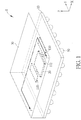
- FIG. 1 is a schematic, perspective diagram of an exemplary Antenna-in-Package (AiP) according to one embodiment of the invention.
- FIG. 2 is a schematic, cross-sectional view taken along line I-I' in FIG. 1 .
- an Antenna-in-Package (AiP) 1 comprises an interface layer 10, an integrated circuit die 20 (shown in phantom in FIG. 1 ) such as a radio-frequency (RF) die disposed on the interface layer 10, a molding compound 30 that is disposed on the interface layer 10 and encapsulates the integrated circuit die 20, and a plurality of solder balls 50 disposed on a bottom surface of the interface layer 10.
- the interface layer 10 electrically connects the integrated circuit die 20 with an external circuit board (not shown) such as a printed circuit board (PCB).
- the interface layer 10 may comprise a substrate, an interconnection structure, a redistribution layer (RDL) structure, an interposer substrate or the like.
- the interface layer 10 may comprise at least an antenna layer 110, a ground reflector layer 120 under the antenna layer 110, and an insulating layer 130 between the antenna layer 110 and the ground reflector layer 120.
- the interface layer 10 may further comprise a plurality of ball pads 122 for attaching the solder balls 50.
- the ball pads 122 and the ground reflector layer 120 are coplanar and are formed in the same metal layer of the interface layer 10.
- the aforesaid ground reflector layer may be disposed within a printed circuit board.
- the ground reflector layer 712 is disposed in a printed circuit board 70.
- the ground reflector layer 712 is disposed directly under the antenna layer 110 and may completely overlap with the antenna layer 110.
- the antenna layer 110 and the ground reflector layer 120 are formed in two different metal layers (e.g., copper layers).
- the two metal layers are in different horizontal planes.
- the interface layer 10 may have an upper surface that is adjacent to the integrated circuit die 20 and a lower surface opposite to the upper surface.
- the antenna layer 110 may be formed at the upper surface and may be electrically connected to the integrated circuit die 20 through an interconnect line or a trace 112.
- the metal layers in the interface layer 10 may be interconnected through conductive vias if necessary.
- the ground reflector layer 120 which may be electrically connected to a ground plane of a printed circuit board (PCB), may be formed at the lower surface of the interface layer 10.
- the ground reflector layer 120 may limit the antenna radiation to the upper hemisphere above the antenna layer 110.
- the ground reflector layer 120 may be a solid metal layer such as a solid copper layer, which completely overlaps with the antenna layer 110 when viewed from the above.
- the integrated circuit die 20 may be an integrated circuit silicon die or a semiconductor chip that comprises relative functional circuits for transmitting and/or receiving mmW or RF signals.
- the integrated circuit die 20 may have an active surface 20a and a passive surface 20b that is opposite to the active surface 20a.
- a plurality of input/output (I/O) pads 210 may be disposed on the active surface 10a.
- the active surface 10a of the integrated circuit die 20 may be integrally joined with the upper surface of the interface layer 10.
- the antenna layer 110 may be electrically connected to respective I/O pads 210 on the active surface 20a of the integrated circuit die 20 through the interconnect or the trace 122.
- the molding compound 30 may comprise organic resin typically used in the encapsulation of integrated circuit devices and selected for low moisture permeability and low thermal coefficient of expansion to avoid exposure of the encapsulated chip to moisture or mechanical stress, respectively.
- the molding compound 30 may comprise epoxy materials.
- the molding compound 30 may further comprise fillers, such as amorphous silicon oxide (silica glass) and crystalline silicon oxide (quartz) fillers. Suitable additives may be added to enhance the thermal conductivity of the molding compound 30.
- the molding compound 30 may have a dielectric constant k ranging between 3.3 and 3.4, for example.
- the molding compound 30 may have a thickness of about 0.4-1.3 mm, for example, 1.2mm.
- the semiconductor package 1 may be a fan-out wafer level package (FOWLP) and the interface layer 10 may be a re-distribution layer (RDL) structure.
- wafer level package involves packaging the die while it is still on the wafer.
- WLP is a substrate-less package. Instead of a substrate, WLP utilizes a thin-film of routing layers, or redistribution layers (RDLs), which provide electrical connections in the package.
- RDLs redistribution layers
- WLP makes use of solder balls 50 on the bottom of the package, which connects the RDLs to a board or a printed circuit board (PCB).
- FIG. 3 is a perspective top view showing an exemplary layout of the integrated circuit die and the antenna elements in the AiP according to one embodiment of the invention.
- the integrated circuit die 20 may have four edges E 1 ⁇ E 4 , which are encapsulated by the molding compound 30.
- a first antenna region 110a of the antenna layer 110 is disposed adjacent to and beyond the first edge E 1 of the integrated circuit die 20.
- a second antenna region 110b of the antenna layer 110 is disposed adjacent to and beyond the second edge E 2 of the integrated circuit die 20, which is opposite to the first edge E 1 .
- the first antenna region 110a is used for transmitting signals and the second antenna region 110b is used for receiving signals.
- the integrated circuit die 20 may comprise a transmitter circuit 201 and a receiver circuit 202, which are electrically coupled to the first antenna region 110a and the second antenna region 110b, respectively.
- the interference between the first antenna region 110a and the second antenna region 110b may be reduced, thereby providing better antenna performance and better isolation between the transmit (Tx) antenna and the receive (Rx) antenna.
- the first antenna region 110a may comprise antenna elements ANT-1 and ANT-2 horizontally extending along a reference X-axis.
- the antenna elements ANT-1 and ANT-2 are two folded dipole antenna elements arranged in parallel with each other.
- the antenna elements ANT-1 and ANT-2 are electrically coupled to the integrated circuit die 20 via a feeding network 140 of power combine.
- the feeding network 140 may comprise two parallel feed lines 141 and 142.
- the feeding network 140 and the antenna elements ANT-1 and ANT-2 are formed in the same antenna layer 110 and are therefore coplanar.
- the feeding network 140 is designed to have intrinsic impedance that can match the impedance of the antenna elements ANT-1 and ANT-2.
- the impedance of the feeding network 140 can be adjusted by, e.g., varying the width of the feed lines 141 and 142 and the size of a gap 143 between the feed lines 141 and 142.
- the gap 143 may have a width of about 20-50 ⁇ m.
- the feed lines 141 and 142 may have a width of about 20-50 ⁇ m.
- the feeding network 140 may be divided into two integral portions: a longitudinal portion 140a extending along the reference Y-axis and a lateral portion 140b extending along the reference X-axis.
- the two distal ends of the longitudinal portion 140a are electrically coupled to the antenna elements ANT-1 and ANT-2, respectively.
- the lateral portion 140b is integrally connected to the longitudinal portion 140a and is electrically coupled to the integrated circuit die 20.
- the folded dipole antenna element ANT-1 comprises a first half-wavelength dipole element 410 comprising first and second quarter-wavelength elements 412 and 414 and a second half-wavelength dipole element 420, which are disposed parallel to each other and separated by a gap 430.
- the gap 143 of the feeding network 140 separates the first half-wavelength dipole element 410 into the first and second quarter-wavelength elements 412 and 414.
- the end portions of elements 412 and 414 are connected (shorted) to end portions of the second half-wavelength dipole element 420 by elements 442 and 444.
- the folded dipole antenna element ANT-1 has a length, denoted as L D , and a width denoted as W D .
- the length L D may range between 900 and 1300 ⁇ m
- the width W D may range between 30 um and 200 ⁇ m.
- the length L D and W D will vary depending on the frequency of operation and the dielectric constant of the substrate.
- the folded dipole antenna element ANT-2 comprises a first half-wavelength dipole element 510 comprising first and second quarter-wavelength elements 512 and 514 and a second half-wavelength dipole element 520, which are disposed parallel to each other and separated by a gap 530.
- the gap 143 of the feeding network 140 separates the first half-wavelength dipole element 510 into the first and second quarter-wavelength elements 512 and 514.
- the end portions of elements 512 and 514 are connected (shorted) to end portions of the second half-wavelength dipole element 520 by elements 542 and 544.
- the dimension (i.e. length and width) of the folded dipole antenna element ANT-2 is the same as that of the folded dipole antenna element ANT-1.
- the folded dipole antenna element ANT-1 is disposed relatively farther away from the integrated circuit die 20 and the folded dipole antenna element ANT-2 is disposed relatively closer to the integrated circuit die 20.
- the distance L 1 between the folded dipole antenna element ANT-1 and the lateral portion 140b of the feeding network 140 is greater than the distance L 2 between the folded dipole antenna element ANT-2 and the lateral portion 140b of the feeding network 140.
- the folded dipole antenna elements ANT-1 and ANT-2 can radiate in phase.
- the second antenna region 110b has a layout that is mirror symmetric to the layout of the first antenna region 110a as described above, with respect to a central axis CA.
- the second antenna region 110b may comprise antenna elements ANT-3 (like ANT-1) and ANT-4 (like ANT-2) horizontally extending along a reference X-axis.
- the antenna elements ANT-3 and ANT-4 are two folded dipole antenna elements arranged in parallel with each other.
- the antenna elements ANT-3 and ANT-4 are electrically coupled to the integrated circuit die 20 via a feeding network 240 of power combine.
- the feeding network 240 may comprise two parallel feed lines 241 and 242.
- the feeding network 240 and the antenna elements ANT-3 and ANT-4 are formed in the same antenna layer 110 and are therefore coplanar.
- the second antenna region 110b may have a layout that is not mirror symmetric to the layout of the first antenna region 110a.
- a first annular guard ring 610a may be provided around the first antenna region 110a, and a second annular guard ring 610b may be provided around the second antenna region 110b.
- the first annular guard ring 610a continuously surrounds the first antenna region 110a and the second annular guard ring 610b continuously surrounds the second antenna region 110b.
- the first annular guard ring 610a and the second annular guard ring 610b are coplanar with the folded dipole antenna elements ANT-1-ANT-4.
- FIG. 4 is a perspective top view of the AiP mounted on a printed circuit board according to one embodiment of the invention.
- the AiP 1 is mounted on a printed circuit board 700 by using surface mount technique (SMT) within a chip mounting area comprising a plurality of ball pads 722.
- SMT surface mount technique
- the layout of the ball pads 722 for the ball grid array on a printed circuit board 700 corresponds to the ball pads 122 at the bottom surface of the AiP 1.
- the mesh type layout of the ground ball pads 722 around the first antennal region 110a and the second antenna region 110b may provide better Tx/Rx isolation and improved SMT quality.
Landscapes
- Engineering & Computer Science (AREA)
- Microelectronics & Electronic Packaging (AREA)
- Physics & Mathematics (AREA)
- Electromagnetism (AREA)
- Variable-Direction Aerials And Aerial Arrays (AREA)
- Details Of Aerials (AREA)
- Geometry (AREA)
- Aerials With Secondary Devices (AREA)
Abstract
Description
- This application claims priority from
U.S. provisional application No. 62/577,747 filed October 27, 2017 - This disclosure relates generally to the field of a semiconductor packaging and, more particularly, to an improved Antenna-in-Package (AiP) with better antenna performance and better isolation between the transmit (Tx) antenna and the receive (Rx) antenna.
- Millimeter-wave (mmW) automotive radar systems are a key technology for future adaptive cruise control systems. With an increased awareness and interest in safety issues on vehicular transportation, a variety of obstacle detectors has been researched and developed, among which a forward looking automotive radar has received special attention as it is considered to be an essential element to complete a vehicular safety system.
- In contrast to infrared or laser-based sensors, the major advantage of a mmW radar system is its excellent performance under adverse weather conditions. Thus, demand for low-cost W-band components has continued to increase, leading to a commercial success of automotive radar systems.
- As known in the art, integration of antenna into a chip package has been fulfilled by adopting the embedded wafer level ball grid array (eWLB) or Antenna-in-Package (AiP) technology. However, there is still a constant need in this industry to provide an AiP with better antenna performance and efficiency.
- The main object of the present invention is to provide an improved Antenna-in-Package (AiP) with better antenna performance and better isolation between the transmit (Tx) antenna and the receive (Rx) antenna.
- According to one aspect of the invention, an Antenna-in-Package (AiP) includes an interface layer, an integrated circuit die disposed on the interface layer, a molding compound disposed on the interface layer and encapsulating the integrated circuit die, and a plurality of solder balls disposed on a bottom surface of the interface layer. The interface layer includes an antenna layer, a ground reflector layer under the antenna layer, and an insulating layer between the antenna layer and the ground reflector layer. The antenna layer includes a first antenna region and a second antenna region spaced apart from the first antenna region. The integrated circuit die is interposed between the first antenna region and the second antenna region. The first antenna region is disposed adjacent to a first edge of the integrated circuit die, and the second antenna region is disposed adjacent to a second edge of the integrated circuit die, which is opposite to the first edge.
- According to some embodiments, the first antenna region is used for transmitting signals and the second antenna region is used for receiving signals.
- According to some embodiments, the interface layer comprises a substrate, an interconnection structure, a redistribution layer (RDL) structure, or an interposer substrate.
- According to some embodiments, the antenna layer and the ground reflector layer are formed in two different metal layers, respectively, which are in different horizontal planes.
- According to some embodiments, the integrated circuit die comprises an integrated circuit silicon die or a semiconductor chip that comprises relative functional circuits for transmitting and receiving millimeter-wave (mmW) or radio-frequency (RF) signals.
- According to some embodiments, the first antenna region comprises a first antenna element, a second antenna element extending along a first direction, a feeding network electrically connecting the first antenna element and the second antenna element to the integrated circuit die.
- According to some embodiments, the first antenna element is disposed relatively farther away from the integrated circuit die and the second antenna element is disposed relatively closer to the integrated circuit die.
- According to some embodiments, the first antenna element and the second antenna element are two folded dipole antenna elements arranged in parallel with each other.
- According to some embodiments, the feeding network, the first antenna element, and the second antenna element are coplanar.
- According to some embodiments, the feeding network comprises two parallel feed lines.
- According to some embodiments, the feeding network is divided into two integral portions: a longitudinal portion extending along a second direction and a lateral portion extending along the first direction.
- According to some embodiments, two distal ends of the longitudinal portion are electrically coupled to the first antenna element and the second antenna element, respectively.
- According to some embodiments, the lateral portion is integrally connected to the longitudinal portion and is electrically coupled to the integrated circuit die.
- According to some embodiments, a distance L1 between the first antenna element and the lateral portion of the feeding network is greater than a distance L2 between the second antenna element and the lateral portion of the feeding network.
- According to some embodiments, a difference between L1 and L2 (L1-L2) is approximately equal to a half wavelength λg, wherein λg is the guided wavelength of electromagnetic radiation transmitted via the antenna layer.
- According to some embodiments, the second antenna region has a layout that is mirror symmetric to a layout of the first antenna region.
- These and other objectives of the present invention will no doubt become obvious to those of ordinary skill in the art after reading the following detailed description of the preferred embodiment that is illustrated in the various figures and drawings.
- The accompanying drawings are included to provide a further understanding of the invention, and are incorporated in and constitute a part of this specification. The drawings illustrate embodiments of the invention and, together with the description, serve to explain the principles of the invention. In the drawings:
-
FIG. 1 is a schematic, perspective diagram of an exemplary Antenna-in-Package (AiP) according to one embodiment of the invention; -
FIG. 2 is a schematic, cross-sectional view taken along line I-I' inFIG. 1 ; -
FIG. 3 is a perspective top view showing an exemplary layout of the integrated circuit die and the antenna elements in the AiP according to one embodiment of the invention; -
FIG. 4 is a perspective top view of the AiP mounted on a printed circuit board according to one embodiment of the invention; and -
FIG. 5 is a schematic, cross-sectional diagram showing that a ground reflector layer is disposed in a printed circuit board according to another embodiment of the invention. - In the following detailed description of the invention, reference is made to the accompanying drawings which form a part hereof, and in which is shown, by way of illustration, specific embodiments in which the invention may be practiced. These embodiments are described in sufficient detail to enable those skilled in the art to practice the invention. Other embodiments may be utilized and structural, logical, and electrical changes may be made without departing from the scope of the present invention.
- The terms "die", "chip", "semiconductor chip", and "semiconductor die" are used interchangeable throughout the specification to mean integrated circuit chip or die. The term "horizontal" as used herein may be defined as a direction parallel to a plane or surface (e.g., surface of a substrate or a stage), regardless of its orientation. The term "vertical," as used herein, may refer to a direction orthogonal to the horizontal direction as just described. Terms, such as "on," "above," "below," "bottom," "top," "side" (as in "sidewall"), "higher," "lower," "upper," "over," and "under," may be referenced with respect to the horizontal plane.
- The present disclosure pertains to an improved Antenna-in-Package (AiP) with better isolation between the transmit (Tx) antenna and the receive (Rx) antenna, which is particularly suited for mmW radar applications such as 77GHz or 79GHz car radar systems for adaptive cruise control, or other automotive radar applications.
- For illustrative purposes, exemplary embodiments of the disclosure will be described with particular reference to folded dipole antenna elements and configuration of such elements in Antenna-in-Package (AiP). It is to be understood, however, that the present invention is not limited to any particular antenna type or operating frequency. Instead, the invention is more generally applicable to any antenna type that is suitable for a given application and/or frequency of operation to provide a high bandwidth and efficiency product antenna.
- Please refer to
FIG. 1 andFIG. 2 .FIG. 1 is a schematic, perspective diagram of an exemplary Antenna-in-Package (AiP) according to one embodiment of the invention.FIG. 2 is a schematic, cross-sectional view taken along line I-I' inFIG. 1 . - As shown in
FIG. 1 andFIG. 2 , according to one embodiment, an Antenna-in-Package (AiP) 1 comprises aninterface layer 10, an integrated circuit die 20 (shown in phantom inFIG. 1 ) such as a radio-frequency (RF) die disposed on theinterface layer 10, amolding compound 30 that is disposed on theinterface layer 10 and encapsulates theintegrated circuit die 20, and a plurality ofsolder balls 50 disposed on a bottom surface of theinterface layer 10. Through thesolder balls 50, theinterface layer 10 electrically connects theintegrated circuit die 20 with an external circuit board (not shown) such as a printed circuit board (PCB). It is understood that theinterface layer 10 may comprise a substrate, an interconnection structure, a redistribution layer (RDL) structure, an interposer substrate or the like. - According to one embodiment of the invention, the
interface layer 10 may comprise at least anantenna layer 110, aground reflector layer 120 under theantenna layer 110, and aninsulating layer 130 between theantenna layer 110 and theground reflector layer 120. Theinterface layer 10 may further comprise a plurality ofball pads 122 for attaching thesolder balls 50. According to one embodiment of the invention, theball pads 122 and theground reflector layer 120 are coplanar and are formed in the same metal layer of theinterface layer 10. - However, it is to be understood that in other embodiments the aforesaid ground reflector layer may be disposed within a printed circuit board. As shown in
FIG. 5 , theground reflector layer 712 is disposed in a printedcircuit board 70. Theground reflector layer 712 is disposed directly under theantenna layer 110 and may completely overlap with theantenna layer 110. - According to one embodiment of the invention, the
antenna layer 110 and theground reflector layer 120 are formed in two different metal layers (e.g., copper layers). The two metal layers are in different horizontal planes. For example, theinterface layer 10 may have an upper surface that is adjacent to the integrated circuit die 20 and a lower surface opposite to the upper surface. Theantenna layer 110 may be formed at the upper surface and may be electrically connected to the integrated circuit die 20 through an interconnect line or atrace 112. Although not shown in the figures, it is to be understood that the metal layers in theinterface layer 10 may be interconnected through conductive vias if necessary. - The
ground reflector layer 120, which may be electrically connected to a ground plane of a printed circuit board (PCB), may be formed at the lower surface of theinterface layer 10. Theground reflector layer 120 may limit the antenna radiation to the upper hemisphere above theantenna layer 110. According to one embodiment of the invention, theground reflector layer 120 may be a solid metal layer such as a solid copper layer, which completely overlaps with theantenna layer 110 when viewed from the above. - According to one embodiment of the invention, the integrated circuit die 20 may be an integrated circuit silicon die or a semiconductor chip that comprises relative functional circuits for transmitting and/or receiving mmW or RF signals. According to one embodiment of the invention, the integrated circuit die 20 may have an
active surface 20a and apassive surface 20b that is opposite to theactive surface 20a. A plurality of input/output (I/O)pads 210 may be disposed on the active surface 10a. According to one embodiment of the invention, the active surface 10a of the integrated circuit die 20 may be integrally joined with the upper surface of theinterface layer 10. Theantenna layer 110 may be electrically connected to respective I/O pads 210 on theactive surface 20a of the integrated circuit die 20 through the interconnect or thetrace 122. - According to one embodiment of the invention, the
molding compound 30 may comprise organic resin typically used in the encapsulation of integrated circuit devices and selected for low moisture permeability and low thermal coefficient of expansion to avoid exposure of the encapsulated chip to moisture or mechanical stress, respectively. For example, according to one embodiment of the invention, themolding compound 30 may comprise epoxy materials. Themolding compound 30 may further comprise fillers, such as amorphous silicon oxide (silica glass) and crystalline silicon oxide (quartz) fillers. Suitable additives may be added to enhance the thermal conductivity of themolding compound 30. According to one embodiment of the invention, themolding compound 30 may have a dielectric constant k ranging between 3.3 and 3.4, for example. According to one embodiment of the invention, themolding compound 30 may have a thickness of about 0.4-1.3 mm, for example, 1.2mm. - According to one embodiment of the invention, the
semiconductor package 1 may be a fan-out wafer level package (FOWLP) and theinterface layer 10 may be a re-distribution layer (RDL) structure. As known in the art, wafer level package (WLP) involves packaging the die while it is still on the wafer. Generally, WLP is a substrate-less package. Instead of a substrate, WLP utilizes a thin-film of routing layers, or redistribution layers (RDLs), which provide electrical connections in the package. WLP makes use ofsolder balls 50 on the bottom of the package, which connects the RDLs to a board or a printed circuit board (PCB). -
FIG. 3 is a perspective top view showing an exemplary layout of the integrated circuit die and the antenna elements in the AiP according to one embodiment of the invention. Referring toFIG. 3 , and briefly back toFIG. 2 , the integrated circuit die 20 may have four edges E1∼E4, which are encapsulated by themolding compound 30. Afirst antenna region 110a of theantenna layer 110 is disposed adjacent to and beyond the first edge E1 of the integrated circuit die 20. Asecond antenna region 110b of theantenna layer 110 is disposed adjacent to and beyond the second edge E2 of the integrated circuit die 20, which is opposite to the first edge E1. According to one embodiment of the invention, thefirst antenna region 110a is used for transmitting signals and thesecond antenna region 110b is used for receiving signals. According to one embodiment of the invention, the integrated circuit die 20 may comprise atransmitter circuit 201 and areceiver circuit 202, which are electrically coupled to thefirst antenna region 110a and thesecond antenna region 110b, respectively. - By separating the
first antenna region 110a from thesecond antenna region 110b with the integrated circuit die 20, the interference between thefirst antenna region 110a and thesecond antenna region 110b may be reduced, thereby providing better antenna performance and better isolation between the transmit (Tx) antenna and the receive (Rx) antenna. - As shown in the enlarged view of
FIG. 3 , thefirst antenna region 110a may comprise antenna elements ANT-1 and ANT-2 horizontally extending along a reference X-axis. According to one exemplary embodiment, the antenna elements ANT-1 and ANT-2 are two folded dipole antenna elements arranged in parallel with each other. The antenna elements ANT-1 and ANT-2 are electrically coupled to the integrated circuit die 20 via afeeding network 140 of power combine. According to one embodiment of the invention, thefeeding network 140 may comprise twoparallel feed lines feeding network 140 and the antenna elements ANT-1 and ANT-2 are formed in thesame antenna layer 110 and are therefore coplanar. - As is known to those skilled in the art, the
feeding network 140 is designed to have intrinsic impedance that can match the impedance of the antenna elements ANT-1 and ANT-2. The impedance of thefeeding network 140 can be adjusted by, e.g., varying the width of thefeed lines gap 143 between thefeed lines gap 143 may have a width of about 20-50µm. According to one embodiment of the invention, for example, thefeed lines - According to one embodiment of the invention, the
feeding network 140 may be divided into two integral portions: alongitudinal portion 140a extending along the reference Y-axis and alateral portion 140b extending along the reference X-axis. The two distal ends of thelongitudinal portion 140a are electrically coupled to the antenna elements ANT-1 and ANT-2, respectively. Thelateral portion 140b is integrally connected to thelongitudinal portion 140a and is electrically coupled to the integrated circuit die 20. - According to one embodiment of the invention, the folded dipole antenna element ANT-1 comprises a first half-
wavelength dipole element 410 comprising first and second quarter-wavelength elements wavelength dipole element 420, which are disposed parallel to each other and separated by agap 430. Thegap 143 of thefeeding network 140 separates the first half-wavelength dipole element 410 into the first and second quarter-wavelength elements elements wavelength dipole element 420 byelements - Likewise, the folded dipole antenna element ANT-2 comprises a first half-
wavelength dipole element 510 comprising first and second quarter-wavelength elements wavelength dipole element 520, which are disposed parallel to each other and separated by agap 530. Thegap 143 of thefeeding network 140 separates the first half-wavelength dipole element 510 into the first and second quarter-wavelength elements elements wavelength dipole element 520 byelements - According to one embodiment of the invention, as shown in
FIG. 3 , the folded dipole antenna element ANT-1 is disposed relatively farther away from the integrated circuit die 20 and the folded dipole antenna element ANT-2 is disposed relatively closer to the integrated circuit die 20. The distance L1 between the folded dipole antenna element ANT-1 and thelateral portion 140b of thefeeding network 140 is greater than the distance L2 between the folded dipole antenna element ANT-2 and thelateral portion 140b of thefeeding network 140. According to one embodiment of the invention, preferably, the difference between L1 and L2 (L1-L2) is approximately equal to a half wavelength λg, wherein λg is the guided wavelength of the electromagnetic radiation transmitted via theantenna layer 110, for example, a W-band radar, operating at 77 GHz, would have a λg=1∼1.5 mm, wherein the substrate dielectric constant (εr) is about 3.6. By providing such configuration, the folded dipole antenna elements ANT-1 and ANT-2 can radiate in phase. - According to one embodiment of the invention, the
second antenna region 110b has a layout that is mirror symmetric to the layout of thefirst antenna region 110a as described above, with respect to a central axis CA. Thesecond antenna region 110b may comprise antenna elements ANT-3 (like ANT-1) and ANT-4 (like ANT-2) horizontally extending along a reference X-axis. According to one exemplary embodiment, the antenna elements ANT-3 and ANT-4 are two folded dipole antenna elements arranged in parallel with each other. The antenna elements ANT-3 and ANT-4 are electrically coupled to the integrated circuit die 20 via afeeding network 240 of power combine. According to one embodiment of the invention, thefeeding network 240 may comprise twoparallel feed lines feeding network 240 and the antenna elements ANT-3 and ANT-4 are formed in thesame antenna layer 110 and are therefore coplanar. - It is to be understood that in other embodiments the
second antenna region 110b may have a layout that is not mirror symmetric to the layout of thefirst antenna region 110a. - According to one embodiment of the invention, as shown in
FIG. 3 , to provide better Tx/Rx isolation, a firstannular guard ring 610a may be provided around thefirst antenna region 110a, and a secondannular guard ring 610b may be provided around thesecond antenna region 110b. The firstannular guard ring 610a continuously surrounds thefirst antenna region 110a and the secondannular guard ring 610b continuously surrounds thesecond antenna region 110b. The firstannular guard ring 610a and the secondannular guard ring 610b are coplanar with the folded dipole antenna elements ANT-1-ANT-4. - Please now refer to
FIG. 4. FIG. 4 is a perspective top view of the AiP mounted on a printed circuit board according to one embodiment of the invention. As shown inFIG. 4 , theAiP 1 is mounted on a printedcircuit board 700 by using surface mount technique (SMT) within a chip mounting area comprising a plurality ofball pads 722. It is to be understood that the layout of theball pads 722 for the ball grid array on a printedcircuit board 700 corresponds to theball pads 122 at the bottom surface of theAiP 1. The mesh type layout of theground ball pads 722 around the firstantennal region 110a and thesecond antenna region 110b may provide better Tx/Rx isolation and improved SMT quality. - Those skilled in the art will readily observe that numerous modifications and alterations of the device and method may be made while retaining the teachings of the invention. Accordingly, the above disclosure should be construed as limited only by the metes and bounds of the appended claims.
Claims (15)
- An Antenna-in-Package, AiP, (1) comprising:an interface layer (10) comprising at least an antenna layer (110) and an insulating layer (130) disposed under the antenna layer (110), wherein the antenna layer (110) comprising a first antenna region and a second antenna region spaced apart from the first antenna region;an integrated circuit die (20) disposed on the interface layer (10), wherein the integrated circuit die (20) is interposed between the first antenna region and the second antenna region, wherein the first antenna region is disposed adjacent to a first edge of the integrated circuit die (20), and the second antenna region is disposed adjacent to a second edge of the integrated circuit die (20), which is opposite to the first edge; anda plurality of solder balls (50) disposed on a bottom surface of the interface layer (10).
- The AiP (1) according to claim 1, wherein the first antenna region is used for transmitting signals and the second antenna region is used for receiving signals; or
wherein the interface layer (10) comprises a substrate, an interconnection structure, a redistribution layer, RDL, structure, or an interposer substrate; or
wherein the AiP (1) further comprises a ground reflector layer, wherein the antenna layer (110) and the ground reflector layer are formed in two different metal layers, respectively, which are in different horizontal planes; or
wherein the integrated circuit die (20) comprises an integrated circuit silicon die or a semiconductor chip that comprises relative functional circuits for transmitting and receiving millimeter-wave, mmW, or radio-frequency, RF, signals. - The AiP (1) according to claim 1, wherein the first antenna region comprises a first antenna element, a second antenna element extending along a first direction, a feeding network electrically connecting the first antenna element and the second antenna element to the integrated circuit die (20).
- The AiP (1) according to claim 3, wherein the first antenna element is disposed relatively farther away from the integrated circuit die (20) and the second antenna element is disposed relatively closer to the integrated circuit die (20); or
the first antenna element and the second antenna element are two folded dipole antenna elements arranged in parallel with each other. - The AiP (1) according to claim 3, wherein the feeding network, the first antenna element, and the second antenna element are coplanar; or
the feeding network comprises two parallel feed lines. - The AiP (1) according to claim 3, wherein the feeding network is divided into two integral portions: a longitudinal portion extending along the second direction and a lateral portion extending along the first direction.
- The AiP (1) according to claim 6, wherein two distal ends of the longitudinal portion are electrically coupled to the first antenna element and the second antenna element, respectively.
- The AiP (1) according to claim 6, wherein the lateral portion is integrally connected to the longitudinal portion and is electrically coupled to the integrated circuit die (20).
- The AiP (1) according to claim 6, wherein a distance L1 between the first antenna element and the lateral portion of the feeding network is greater than a distance L2 between the second antenna element and the lateral portion of the feeding network.
- The AiP (1) according to claim 9, wherein a difference between L1 and L2 is approximately equal to a half wavelength λg, wherein λg is the guided wavelength of electromagnetic radiation transmitted via the antenna layer (110).
- The AiP (1) according to claim 1, wherein the second antenna region has a layout that is mirror symmetric to a layout of the first antenna region.
- The AiP (1) according to claim 3 further comprising:a first annular guard ring provided around the first antenna region; anda second annular guard ring provided around the second antenna region, wherein the first annular guard ring continuously surrounds the first antenna region and the second annular guard ring continuously surrounds the second antenna region.
- The AiP (1) according to claim 12, wherein first annular guard ring and the second annular guard ring are coplanar with the first and second antenna elements.
- The AiP (1) according to claim 1 further comprising:a mesh type layout of ground ball pads around the first antenna region and the second antenna region.
- An Antenna-in-Package, AiP, (1) comprising:an interface layer (10) comprising at least an antenna layer (110) and an insulating layer (130) disposed under the antenna layer (110), wherein the antenna layer (110) comprising a first antenna region and a second antenna region spaced apart from the first antenna region;an integrated circuit die (20) disposed on the interface layer (10), wherein the integrated circuit die (20) is interposed between the first antenna region and the second antenna region, wherein the first antenna region is disposed adjacent to a first edge of the integrated circuit die (20), and the second antenna region is disposed adjacent to a second edge of the integrated circuit die (20), which is opposite to the first edge;a plurality of solder balls (50) disposed on a bottom surface of the interface layer (10); anda printed circuit board, PCB, comprising a ground reflector layer, wherein the interface layer (10) disposed on the PCB via the plurality of solder balls (50).
Applications Claiming Priority (2)
| Application Number | Priority Date | Filing Date | Title |
|---|---|---|---|
| US201762577747P | 2017-10-27 | 2017-10-27 | |
| US16/145,108 US10700410B2 (en) | 2017-10-27 | 2018-09-27 | Antenna-in-package with better antenna performance |
Publications (2)
| Publication Number | Publication Date |
|---|---|
| EP3477767A1 true EP3477767A1 (en) | 2019-05-01 |
| EP3477767B1 EP3477767B1 (en) | 2021-03-10 |
Family
ID=63921510
Family Applications (1)
| Application Number | Title | Priority Date | Filing Date |
|---|---|---|---|
| EP18200638.7A Active EP3477767B1 (en) | 2017-10-27 | 2018-10-16 | Antenna-in-package with better antenna performance |
Country Status (4)
| Country | Link |
|---|---|
| US (2) | US10700410B2 (en) |
| EP (1) | EP3477767B1 (en) |
| CN (2) | CN109950682B (en) |
| TW (1) | TWI674656B (en) |
Families Citing this family (12)
| Publication number | Priority date | Publication date | Assignee | Title |
|---|---|---|---|---|
| US10483617B2 (en) * | 2017-09-29 | 2019-11-19 | Taiwan Semiconductor Manufacturing Co., Ltd. | Package structure |
| US11322823B2 (en) | 2017-10-17 | 2022-05-03 | Mediatek Inc. | Antenna-in-package with frequency-selective surface structure |
| DE102018129019A1 (en) * | 2018-05-21 | 2019-11-21 | Taiwan Semiconductor Manufacturing Co., Ltd. | SEMICONDUCTOR DEVICE AND METHOD OF MANUFACTURE |
| US11201119B2 (en) | 2018-06-06 | 2021-12-14 | At&S Austria Technologie & Systemtechnik Aktiengesellschaft | RF functionality and electromagnetic radiation shielding in a component carrier |
| CN109088180B (en) * | 2018-08-12 | 2020-11-20 | 瑞声科技(南京)有限公司 | AOG antenna system and mobile terminal |
| KR102499038B1 (en) * | 2018-12-06 | 2023-02-13 | 삼성전자주식회사 | Antenna module |
| US11244913B2 (en) * | 2019-06-18 | 2022-02-08 | Mediatek Inc. | Semiconductor package |
| KR102568702B1 (en) | 2019-10-15 | 2023-08-21 | 삼성전자주식회사 | Antenna sturcture and electronic device including the same |
| EP4044366B1 (en) * | 2021-02-12 | 2023-10-25 | Sivers Wireless AB | An integrated circuit package comprising a crossed dipole antenna |
| KR102933007B1 (en) | 2021-05-24 | 2026-03-04 | 삼성전자주식회사 | Antenna module and apparatus including thereof |
| US12438007B2 (en) | 2021-11-12 | 2025-10-07 | Taiwan Semiconductor Manufacturing Co., Ltd. | Staggered metal mesh on backside of device die and method forming same |
| CN115189135A (en) * | 2022-08-10 | 2022-10-14 | 航天恒星科技有限公司 | Common-caliber AiP integrated satellite-borne phased array antenna |
Citations (2)
| Publication number | Priority date | Publication date | Assignee | Title |
|---|---|---|---|---|
| US20130141284A1 (en) * | 2011-12-05 | 2013-06-06 | Samsung Electro-Mechanics Co., Ltd. | Rfic antenna package for millimeter band and rf module including the same |
| US20160020524A1 (en) * | 2010-12-20 | 2016-01-21 | Stmicroelectronics Sa | Integrated millimeter wave transceiver |
Family Cites Families (41)
| Publication number | Priority date | Publication date | Assignee | Title |
|---|---|---|---|---|
| CA2241128A1 (en) * | 1997-06-30 | 1998-12-30 | Sony International (Europe) Gmbh | Wide band printed phase array antenna for microwave and mm-wave applications |
| AU778969B2 (en) * | 1999-11-03 | 2004-12-23 | Andrew Corporation | Folded dipole antenna |
| EP1413004A4 (en) | 2001-05-17 | 2004-07-21 | Cypress Semiconductor Corp | BALL MATRIX GRID ANTENNA |
| US6770955B1 (en) * | 2001-12-15 | 2004-08-03 | Skyworks Solutions, Inc. | Shielded antenna in a semiconductor package |
| US7119745B2 (en) * | 2004-06-30 | 2006-10-10 | International Business Machines Corporation | Apparatus and method for constructing and packaging printed antenna devices |
| US20060276157A1 (en) | 2005-06-03 | 2006-12-07 | Chen Zhi N | Apparatus and methods for packaging antennas with integrated circuit chips for millimeter wave applications |
| CA2611620A1 (en) | 2005-06-09 | 2006-12-21 | Lester E. Burgess | Hybrid conductive coating method for electrical bridging connection of rfid die chip to composite antenna |
| TWM293545U (en) * | 2006-01-13 | 2006-07-01 | Cameo Communications Inc | Patch antenna, and wireless networking device with the same |
| CN2919568Y (en) * | 2006-01-26 | 2007-07-04 | 友劲科技股份有限公司 | Panel Antennas for Wireless Networking Devices |
| TW200816562A (en) * | 2006-09-29 | 2008-04-01 | Z Com Inc | Dipole antenna and dipole array antenna |
| US8164167B2 (en) | 2007-03-09 | 2012-04-24 | Nanyang Technological University | Integrated circuit structure and a method of forming the same |
| US7692590B2 (en) * | 2008-02-20 | 2010-04-06 | International Business Machines Corporation | Radio frequency (RF) integrated circuit (IC) packages with integrated aperture-coupled patch antenna(s) |
| US7696930B2 (en) * | 2008-04-14 | 2010-04-13 | International Business Machines Corporation | Radio frequency (RF) integrated circuit (IC) packages with integrated aperture-coupled patch antenna(s) in ring and/or offset cavities |
| TWI382595B (en) * | 2008-09-16 | 2013-01-11 | Polychem Uv Eb Internat Corp | Antenna construction of RFID transponder and its manufacturing method |
| CN201298593Y (en) * | 2008-10-20 | 2009-08-26 | 青岛市广播电视局 | Double trifurcate transmitting antenna |
| US8278749B2 (en) * | 2009-01-30 | 2012-10-02 | Infineon Technologies Ag | Integrated antennas in wafer level package |
| FR2952457B1 (en) * | 2009-11-10 | 2011-12-16 | St Microelectronics Sa | ELECTRONIC DEVICE COMPRISING A SEMICONDUCTOR COMPONENT INTEGRATING AN ANTENNA |
| CN201781071U (en) * | 2010-08-03 | 2011-03-30 | 惠州Tcl移动通信有限公司 | Broadband antenna and feed network |
| US8451618B2 (en) * | 2010-10-28 | 2013-05-28 | Infineon Technologies Ag | Integrated antennas in wafer level package |
| CN103460821B (en) * | 2011-04-01 | 2016-08-10 | 株式会社村田制作所 | Component built-in resin substrate and manufacturing method thereof |
| WO2012137548A1 (en) * | 2011-04-04 | 2012-10-11 | 株式会社村田製作所 | Multilayer substrate with integrated chip component and method for manufacturing same |
| CN102394350A (en) * | 2011-07-12 | 2012-03-28 | 瑞声声学科技(深圳)有限公司 | Foldable dipole antenna |
| CN102522628B (en) * | 2011-12-09 | 2014-05-14 | 清华大学 | High gain bidirectional end-fire antenna array applied to mine and tunnel |
| US9711465B2 (en) * | 2012-05-29 | 2017-07-18 | Taiwan Semiconductor Manufacturing Co., Ltd. | Antenna cavity structure for integrated patch antenna in integrated fan-out packaging |
| US9252491B2 (en) * | 2012-11-30 | 2016-02-02 | Taiwan Semiconductor Manufacturing Company, Ltd. | Embedding low-k materials in antennas |
| US9806422B2 (en) * | 2013-09-11 | 2017-10-31 | International Business Machines Corporation | Antenna-in-package structures with broadside and end-fire radiations |
| CN104518279A (en) * | 2013-09-30 | 2015-04-15 | 西门子(中国)有限公司 | Bidirectional antenna, wireless access point and train control system |
| EP3176734B1 (en) * | 2014-11-27 | 2020-07-15 | Murata Manufacturing Co., Ltd. | Rfic module and rfid tag equipped with same |
| TWI549365B (en) * | 2014-12-02 | 2016-09-11 | Hongbo Wireless Comm Technology Co Ltd | Antenna array of hybrid radiator elements |
| US10317512B2 (en) * | 2014-12-23 | 2019-06-11 | Infineon Technologies Ag | RF system with an RFIC and antenna system |
| US9768837B2 (en) * | 2015-12-17 | 2017-09-19 | Humatics Corporation | Radio-frequency localization techniques and associated systems, devices, and methods |
| CN209328060U (en) * | 2015-12-21 | 2019-08-30 | 株式会社村田制作所 | Component built-in device |
| US9881882B2 (en) | 2016-01-06 | 2018-01-30 | Mediatek Inc. | Semiconductor package with three-dimensional antenna |
| JP2017157961A (en) * | 2016-02-29 | 2017-09-07 | パナソニック株式会社 | Antenna board |
| CN105789872A (en) * | 2016-03-25 | 2016-07-20 | 广东工业大学 | Compact circular polarization array antenna of 5.8GHzISA frequency range |
| WO2018094660A1 (en) * | 2016-11-24 | 2018-05-31 | 深圳市大疆创新科技有限公司 | Antenna assembly and unmanned aerial vehicle |
| US10085342B2 (en) * | 2016-12-13 | 2018-09-25 | Intel Corporation | Microelectronic device having an air core inductor |
| JP6593552B2 (en) * | 2017-03-09 | 2019-10-23 | 株式会社村田製作所 | Wireless communication device |
| US10411328B2 (en) * | 2017-09-15 | 2019-09-10 | Taiwan Semiconductor Manufacturing Company, Ltd. | Patch antenna structures and methods |
| US11024979B2 (en) * | 2017-09-29 | 2021-06-01 | Taiwan Semiconductor Manufacturing Co., Ltd. | 3D IC antenna array with laminated high-k dielectric |
| US10872842B2 (en) * | 2019-02-25 | 2020-12-22 | Taiwan Semiconductor Manufacturing Company, Ltd. | Semiconductor device and manufacturing method thereof |
-
2018
- 2018-09-27 US US16/145,108 patent/US10700410B2/en active Active
- 2018-10-16 EP EP18200638.7A patent/EP3477767B1/en active Active
- 2018-10-26 CN CN201811258868.6A patent/CN109950682B/en active Active
- 2018-10-26 TW TW107137950A patent/TWI674656B/en active
- 2018-10-26 CN CN202110368721.8A patent/CN113328231B/en active Active
-
2020
- 2020-05-27 US US16/884,064 patent/US11050135B2/en active Active
Patent Citations (2)
| Publication number | Priority date | Publication date | Assignee | Title |
|---|---|---|---|---|
| US20160020524A1 (en) * | 2010-12-20 | 2016-01-21 | Stmicroelectronics Sa | Integrated millimeter wave transceiver |
| US20130141284A1 (en) * | 2011-12-05 | 2013-06-06 | Samsung Electro-Mechanics Co., Ltd. | Rfic antenna package for millimeter band and rf module including the same |
Non-Patent Citations (2)
| Title |
|---|
| STEFAN BEER ET AL: "A 122 GHz four element patch array fed by electromagnetic coupling", MICROWAVE WORKSHOP SERIES ON MILLIMETER WAVE WIRELESS TECHNOLOGY AND APPLICATIONS (IMWS), 2012 IEEE MTT-S INTERNATIONAL, IEEE, 18 September 2012 (2012-09-18), pages 1 - 4, XP032264451, ISBN: 978-1-4673-0901-1, DOI: 10.1109/IMWS2.2012.6338169 * |
| ZWICK T ET AL: "Broadband Planar Superstrate Antenna for Integrated Millimeterwave Transceivers", IEEE TRANSACTIONS ON ANTENNAS AND PROPAGATION, IEEE SERVICE CENTER, PISCATAWAY, NJ, US, vol. 54, no. 10, 1 October 2006 (2006-10-01), pages 2790 - 2796, XP001545348, ISSN: 0018-926X, DOI: 10.1109/TAP.2006.882167 * |
Also Published As
| Publication number | Publication date |
|---|---|
| US20190131690A1 (en) | 2019-05-02 |
| CN113328231B (en) | 2024-06-28 |
| US20200287271A1 (en) | 2020-09-10 |
| CN109950682A (en) | 2019-06-28 |
| EP3477767B1 (en) | 2021-03-10 |
| US10700410B2 (en) | 2020-06-30 |
| TW201917836A (en) | 2019-05-01 |
| CN109950682B (en) | 2021-04-30 |
| US11050135B2 (en) | 2021-06-29 |
| TWI674656B (en) | 2019-10-11 |
| CN113328231A (en) | 2021-08-31 |
Similar Documents
| Publication | Publication Date | Title |
|---|---|---|
| US11050135B2 (en) | Antenna-in-package with better antenna performance | |
| US10916854B2 (en) | Antenna structure with integrated coupling element and semiconductor package using the same | |
| US11848481B2 (en) | Antenna-in-package with frequency-selective surface structure | |
| CN108231750B (en) | RF device package and method of forming the same | |
| US8648454B2 (en) | Wafer-scale package structures with integrated antennas | |
| US11821975B2 (en) | Radar module incorporated with a pattern-shaping device | |
| US9172131B2 (en) | Semiconductor structure having aperture antenna | |
| EP3413347A1 (en) | Semiconductor package having discrete antenna device | |
| US9349696B2 (en) | Integrated antennas in wafer level package | |
| US8866292B2 (en) | Semiconductor packages with integrated antenna and methods of forming thereof | |
| CN113646890A (en) | On-Package Antenna IC Device | |
| US11715886B2 (en) | Low-cost, IPD and laminate based antenna array module | |
| US20190173176A1 (en) | Antenna apparatus and antenna module | |
| WO2017111766A1 (en) | Microelectronic devices designed with high frequency communication devices including compound semiconductor devices integrated on a die fabric on package | |
| CN113678250A (en) | On-Package Antenna IC Device | |
| US20230290700A1 (en) | Antenna package | |
| CN116742316A (en) | An antenna package | |
| US11416730B2 (en) | Radio-frequency device with radio-frequency signal carrying element and associated production method |
Legal Events
| Date | Code | Title | Description |
|---|---|---|---|
| PUAI | Public reference made under article 153(3) epc to a published international application that has entered the european phase |
Free format text: ORIGINAL CODE: 0009012 |
|
| STAA | Information on the status of an ep patent application or granted ep patent |
Free format text: STATUS: THE APPLICATION HAS BEEN PUBLISHED |
|
| AK | Designated contracting states |
Kind code of ref document: A1 Designated state(s): AL AT BE BG CH CY CZ DE DK EE ES FI FR GB GR HR HU IE IS IT LI LT LU LV MC MK MT NL NO PL PT RO RS SE SI SK SM TR |
|
| AX | Request for extension of the european patent |
Extension state: BA ME |
|
| STAA | Information on the status of an ep patent application or granted ep patent |
Free format text: STATUS: REQUEST FOR EXAMINATION WAS MADE |
|
| 17P | Request for examination filed |
Effective date: 20191017 |
|
| RBV | Designated contracting states (corrected) |
Designated state(s): AL AT BE BG CH CY CZ DE DK EE ES FI FR GB GR HR HU IE IS IT LI LT LU LV MC MK MT NL NO PL PT RO RS SE SI SK SM TR |
|
| STAA | Information on the status of an ep patent application or granted ep patent |
Free format text: STATUS: EXAMINATION IS IN PROGRESS |
|
| 17Q | First examination report despatched |
Effective date: 20200306 |
|
| GRAP | Despatch of communication of intention to grant a patent |
Free format text: ORIGINAL CODE: EPIDOSNIGR1 |
|
| STAA | Information on the status of an ep patent application or granted ep patent |
Free format text: STATUS: GRANT OF PATENT IS INTENDED |
|
| INTG | Intention to grant announced |
Effective date: 20201001 |
|
| GRAS | Grant fee paid |
Free format text: ORIGINAL CODE: EPIDOSNIGR3 |
|
| GRAA | (expected) grant |
Free format text: ORIGINAL CODE: 0009210 |
|
| STAA | Information on the status of an ep patent application or granted ep patent |
Free format text: STATUS: THE PATENT HAS BEEN GRANTED |
|
| AK | Designated contracting states |
Kind code of ref document: B1 Designated state(s): AL AT BE BG CH CY CZ DE DK EE ES FI FR GB GR HR HU IE IS IT LI LT LU LV MC MK MT NL NO PL PT RO RS SE SI SK SM TR |
|
| REG | Reference to a national code |
Ref country code: GB Ref legal event code: FG4D |
|
| REG | Reference to a national code |
Ref country code: AT Ref legal event code: REF Ref document number: 1370820 Country of ref document: AT Kind code of ref document: T Effective date: 20210315 Ref country code: CH Ref legal event code: EP |
|
| REG | Reference to a national code |
Ref country code: IE Ref legal event code: FG4D |
|
| REG | Reference to a national code |
Ref country code: DE Ref legal event code: R096 Ref document number: 602018013658 Country of ref document: DE |
|
| REG | Reference to a national code |
Ref country code: LT Ref legal event code: MG9D |
|
| PG25 | Lapsed in a contracting state [announced via postgrant information from national office to epo] |
Ref country code: NO Free format text: LAPSE BECAUSE OF FAILURE TO SUBMIT A TRANSLATION OF THE DESCRIPTION OR TO PAY THE FEE WITHIN THE PRESCRIBED TIME-LIMIT Effective date: 20210610 Ref country code: LT Free format text: LAPSE BECAUSE OF FAILURE TO SUBMIT A TRANSLATION OF THE DESCRIPTION OR TO PAY THE FEE WITHIN THE PRESCRIBED TIME-LIMIT Effective date: 20210310 Ref country code: BG Free format text: LAPSE BECAUSE OF FAILURE TO SUBMIT A TRANSLATION OF THE DESCRIPTION OR TO PAY THE FEE WITHIN THE PRESCRIBED TIME-LIMIT Effective date: 20210610 Ref country code: HR Free format text: LAPSE BECAUSE OF FAILURE TO SUBMIT A TRANSLATION OF THE DESCRIPTION OR TO PAY THE FEE WITHIN THE PRESCRIBED TIME-LIMIT Effective date: 20210310 Ref country code: FI Free format text: LAPSE BECAUSE OF FAILURE TO SUBMIT A TRANSLATION OF THE DESCRIPTION OR TO PAY THE FEE WITHIN THE PRESCRIBED TIME-LIMIT Effective date: 20210310 Ref country code: GR Free format text: LAPSE BECAUSE OF FAILURE TO SUBMIT A TRANSLATION OF THE DESCRIPTION OR TO PAY THE FEE WITHIN THE PRESCRIBED TIME-LIMIT Effective date: 20210611 |
|
| REG | Reference to a national code |
Ref country code: AT Ref legal event code: MK05 Ref document number: 1370820 Country of ref document: AT Kind code of ref document: T Effective date: 20210310 |
|
| REG | Reference to a national code |
Ref country code: NL Ref legal event code: MP Effective date: 20210310 |
|
| PG25 | Lapsed in a contracting state [announced via postgrant information from national office to epo] |
Ref country code: RS Free format text: LAPSE BECAUSE OF FAILURE TO SUBMIT A TRANSLATION OF THE DESCRIPTION OR TO PAY THE FEE WITHIN THE PRESCRIBED TIME-LIMIT Effective date: 20210310 Ref country code: LV Free format text: LAPSE BECAUSE OF FAILURE TO SUBMIT A TRANSLATION OF THE DESCRIPTION OR TO PAY THE FEE WITHIN THE PRESCRIBED TIME-LIMIT Effective date: 20210310 Ref country code: SE Free format text: LAPSE BECAUSE OF FAILURE TO SUBMIT A TRANSLATION OF THE DESCRIPTION OR TO PAY THE FEE WITHIN THE PRESCRIBED TIME-LIMIT Effective date: 20210310 |
|
| PG25 | Lapsed in a contracting state [announced via postgrant information from national office to epo] |
Ref country code: NL Free format text: LAPSE BECAUSE OF FAILURE TO SUBMIT A TRANSLATION OF THE DESCRIPTION OR TO PAY THE FEE WITHIN THE PRESCRIBED TIME-LIMIT Effective date: 20210310 |
|
| PG25 | Lapsed in a contracting state [announced via postgrant information from national office to epo] |
Ref country code: AT Free format text: LAPSE BECAUSE OF FAILURE TO SUBMIT A TRANSLATION OF THE DESCRIPTION OR TO PAY THE FEE WITHIN THE PRESCRIBED TIME-LIMIT Effective date: 20210310 Ref country code: SM Free format text: LAPSE BECAUSE OF FAILURE TO SUBMIT A TRANSLATION OF THE DESCRIPTION OR TO PAY THE FEE WITHIN THE PRESCRIBED TIME-LIMIT Effective date: 20210310 Ref country code: CZ Free format text: LAPSE BECAUSE OF FAILURE TO SUBMIT A TRANSLATION OF THE DESCRIPTION OR TO PAY THE FEE WITHIN THE PRESCRIBED TIME-LIMIT Effective date: 20210310 Ref country code: EE Free format text: LAPSE BECAUSE OF FAILURE TO SUBMIT A TRANSLATION OF THE DESCRIPTION OR TO PAY THE FEE WITHIN THE PRESCRIBED TIME-LIMIT Effective date: 20210310 |
|
| PG25 | Lapsed in a contracting state [announced via postgrant information from national office to epo] |
Ref country code: IS Free format text: LAPSE BECAUSE OF FAILURE TO SUBMIT A TRANSLATION OF THE DESCRIPTION OR TO PAY THE FEE WITHIN THE PRESCRIBED TIME-LIMIT Effective date: 20210710 Ref country code: RO Free format text: LAPSE BECAUSE OF FAILURE TO SUBMIT A TRANSLATION OF THE DESCRIPTION OR TO PAY THE FEE WITHIN THE PRESCRIBED TIME-LIMIT Effective date: 20210310 Ref country code: SK Free format text: LAPSE BECAUSE OF FAILURE TO SUBMIT A TRANSLATION OF THE DESCRIPTION OR TO PAY THE FEE WITHIN THE PRESCRIBED TIME-LIMIT Effective date: 20210310 Ref country code: PL Free format text: LAPSE BECAUSE OF FAILURE TO SUBMIT A TRANSLATION OF THE DESCRIPTION OR TO PAY THE FEE WITHIN THE PRESCRIBED TIME-LIMIT Effective date: 20210310 Ref country code: PT Free format text: LAPSE BECAUSE OF FAILURE TO SUBMIT A TRANSLATION OF THE DESCRIPTION OR TO PAY THE FEE WITHIN THE PRESCRIBED TIME-LIMIT Effective date: 20210712 |
|
| REG | Reference to a national code |
Ref country code: DE Ref legal event code: R097 Ref document number: 602018013658 Country of ref document: DE |
|
| PLBE | No opposition filed within time limit |
Free format text: ORIGINAL CODE: 0009261 |
|
| STAA | Information on the status of an ep patent application or granted ep patent |
Free format text: STATUS: NO OPPOSITION FILED WITHIN TIME LIMIT |
|
| PG25 | Lapsed in a contracting state [announced via postgrant information from national office to epo] |
Ref country code: ES Free format text: LAPSE BECAUSE OF FAILURE TO SUBMIT A TRANSLATION OF THE DESCRIPTION OR TO PAY THE FEE WITHIN THE PRESCRIBED TIME-LIMIT Effective date: 20210310 Ref country code: DK Free format text: LAPSE BECAUSE OF FAILURE TO SUBMIT A TRANSLATION OF THE DESCRIPTION OR TO PAY THE FEE WITHIN THE PRESCRIBED TIME-LIMIT Effective date: 20210310 Ref country code: AL Free format text: LAPSE BECAUSE OF FAILURE TO SUBMIT A TRANSLATION OF THE DESCRIPTION OR TO PAY THE FEE WITHIN THE PRESCRIBED TIME-LIMIT Effective date: 20210310 |
|
| 26N | No opposition filed |
Effective date: 20211213 |
|
| PG25 | Lapsed in a contracting state [announced via postgrant information from national office to epo] |
Ref country code: SI Free format text: LAPSE BECAUSE OF FAILURE TO SUBMIT A TRANSLATION OF THE DESCRIPTION OR TO PAY THE FEE WITHIN THE PRESCRIBED TIME-LIMIT Effective date: 20210310 |
|
| PG25 | Lapsed in a contracting state [announced via postgrant information from national office to epo] |
Ref country code: IT Free format text: LAPSE BECAUSE OF FAILURE TO SUBMIT A TRANSLATION OF THE DESCRIPTION OR TO PAY THE FEE WITHIN THE PRESCRIBED TIME-LIMIT Effective date: 20210310 |
|
| REG | Reference to a national code |
Ref country code: CH Ref legal event code: PL |
|
| PG25 | Lapsed in a contracting state [announced via postgrant information from national office to epo] |
Ref country code: IS Free format text: LAPSE BECAUSE OF FAILURE TO SUBMIT A TRANSLATION OF THE DESCRIPTION OR TO PAY THE FEE WITHIN THE PRESCRIBED TIME-LIMIT Effective date: 20210710 |
|
| REG | Reference to a national code |
Ref country code: BE Ref legal event code: MM Effective date: 20211031 |
|
| PG25 | Lapsed in a contracting state [announced via postgrant information from national office to epo] |
Ref country code: MC Free format text: LAPSE BECAUSE OF FAILURE TO SUBMIT A TRANSLATION OF THE DESCRIPTION OR TO PAY THE FEE WITHIN THE PRESCRIBED TIME-LIMIT Effective date: 20210310 |
|
| PG25 | Lapsed in a contracting state [announced via postgrant information from national office to epo] |
Ref country code: LU Free format text: LAPSE BECAUSE OF NON-PAYMENT OF DUE FEES Effective date: 20211016 Ref country code: BE Free format text: LAPSE BECAUSE OF NON-PAYMENT OF DUE FEES Effective date: 20211031 |
|
| PG25 | Lapsed in a contracting state [announced via postgrant information from national office to epo] |
Ref country code: LI Free format text: LAPSE BECAUSE OF NON-PAYMENT OF DUE FEES Effective date: 20211031 Ref country code: CH Free format text: LAPSE BECAUSE OF NON-PAYMENT OF DUE FEES Effective date: 20211031 |
|
| PG25 | Lapsed in a contracting state [announced via postgrant information from national office to epo] |
Ref country code: IE Free format text: LAPSE BECAUSE OF NON-PAYMENT OF DUE FEES Effective date: 20211016 |
|
| PG25 | Lapsed in a contracting state [announced via postgrant information from national office to epo] |
Ref country code: CY Free format text: LAPSE BECAUSE OF FAILURE TO SUBMIT A TRANSLATION OF THE DESCRIPTION OR TO PAY THE FEE WITHIN THE PRESCRIBED TIME-LIMIT Effective date: 20210310 |
|
| P01 | Opt-out of the competence of the unified patent court (upc) registered |
Effective date: 20230607 |
|
| PG25 | Lapsed in a contracting state [announced via postgrant information from national office to epo] |
Ref country code: HU Free format text: LAPSE BECAUSE OF FAILURE TO SUBMIT A TRANSLATION OF THE DESCRIPTION OR TO PAY THE FEE WITHIN THE PRESCRIBED TIME-LIMIT; INVALID AB INITIO Effective date: 20181016 |
|
| PG25 | Lapsed in a contracting state [announced via postgrant information from national office to epo] |
Ref country code: MK Free format text: LAPSE BECAUSE OF FAILURE TO SUBMIT A TRANSLATION OF THE DESCRIPTION OR TO PAY THE FEE WITHIN THE PRESCRIBED TIME-LIMIT Effective date: 20210310 |
|
| PG25 | Lapsed in a contracting state [announced via postgrant information from national office to epo] |
Ref country code: MT Free format text: LAPSE BECAUSE OF FAILURE TO SUBMIT A TRANSLATION OF THE DESCRIPTION OR TO PAY THE FEE WITHIN THE PRESCRIBED TIME-LIMIT Effective date: 20210310 |
|
| PGFP | Annual fee paid to national office [announced via postgrant information from national office to epo] |
Ref country code: GB Payment date: 20250828 Year of fee payment: 8 |
|
| PGFP | Annual fee paid to national office [announced via postgrant information from national office to epo] |
Ref country code: FR Payment date: 20250808 Year of fee payment: 8 |
|
| PG25 | Lapsed in a contracting state [announced via postgrant information from national office to epo] |
Ref country code: TR Free format text: LAPSE BECAUSE OF FAILURE TO SUBMIT A TRANSLATION OF THE DESCRIPTION OR TO PAY THE FEE WITHIN THE PRESCRIBED TIME-LIMIT Effective date: 20210310 |
|
| PGFP | Annual fee paid to national office [announced via postgrant information from national office to epo] |
Ref country code: DE Payment date: 20250819 Year of fee payment: 8 |