EP3477715A1 - Piezoelectric mems device having a suspended diaphragm and manufacturing process thereof - Google Patents
Piezoelectric mems device having a suspended diaphragm and manufacturing process thereof Download PDFInfo
- Publication number
- EP3477715A1 EP3477715A1 EP18203888.5A EP18203888A EP3477715A1 EP 3477715 A1 EP3477715 A1 EP 3477715A1 EP 18203888 A EP18203888 A EP 18203888A EP 3477715 A1 EP3477715 A1 EP 3477715A1
- Authority
- EP
- European Patent Office
- Prior art keywords
- cavity
- recess
- forming
- extending
- deformable portion
- Prior art date
- Legal status (The legal status is an assumption and is not a legal conclusion. Google has not performed a legal analysis and makes no representation as to the accuracy of the status listed.)
- Granted
Links
Images





Classifications
-
- B—PERFORMING OPERATIONS; TRANSPORTING
- B81—MICROSTRUCTURAL TECHNOLOGY
- B81B—MICROSTRUCTURAL DEVICES OR SYSTEMS, e.g. MICROMECHANICAL DEVICES
- B81B3/00—Devices comprising flexible or deformable elements, e.g. comprising elastic tongues or membranes
- B81B3/0018—Structures acting upon the moving or flexible element for transforming energy into mechanical movement or vice versa, i.e. actuators, sensors, generators
- B81B3/0021—Transducers for transforming electrical into mechanical energy or vice versa
-
- B—PERFORMING OPERATIONS; TRANSPORTING
- B81—MICROSTRUCTURAL TECHNOLOGY
- B81B—MICROSTRUCTURAL DEVICES OR SYSTEMS, e.g. MICROMECHANICAL DEVICES
- B81B3/00—Devices comprising flexible or deformable elements, e.g. comprising elastic tongues or membranes
- B81B3/0035—Constitution or structural means for controlling the movement of the flexible or deformable elements
- B81B3/0051—For defining the movement, i.e. structures that guide or limit the movement of an element
-
- B—PERFORMING OPERATIONS; TRANSPORTING
- B81—MICROSTRUCTURAL TECHNOLOGY
- B81C—PROCESSES OR APPARATUS SPECIALLY ADAPTED FOR THE MANUFACTURE OR TREATMENT OF MICROSTRUCTURAL DEVICES OR SYSTEMS
- B81C1/00—Manufacture or treatment of devices or systems in or on a substrate
- B81C1/00015—Manufacture or treatment of devices or systems in or on a substrate for manufacturing microsystems
- B81C1/00134—Manufacture or treatment of devices or systems in or on a substrate for manufacturing microsystems comprising flexible or deformable structures
- B81C1/00158—Diaphragms, membranes
-
- G—PHYSICS
- G02—OPTICS
- G02B—OPTICAL ELEMENTS, SYSTEMS OR APPARATUS
- G02B26/00—Optical devices or arrangements for the control of light using movable or deformable optical elements
- G02B26/08—Optical devices or arrangements for the control of light using movable or deformable optical elements for controlling the direction of light
- G02B26/0875—Optical devices or arrangements for the control of light using movable or deformable optical elements for controlling the direction of light by means of one or more refracting elements
-
- G—PHYSICS
- G02—OPTICS
- G02B—OPTICAL ELEMENTS, SYSTEMS OR APPARATUS
- G02B3/00—Simple or compound lenses
- G02B3/12—Fluid-filled or evacuated lenses
- G02B3/14—Fluid-filled or evacuated lenses of variable focal length
-
- H—ELECTRICITY
- H10—SEMICONDUCTOR DEVICES; ELECTRIC SOLID-STATE DEVICES NOT OTHERWISE PROVIDED FOR
- H10N—ELECTRIC SOLID-STATE DEVICES NOT OTHERWISE PROVIDED FOR
- H10N30/00—Piezoelectric or electrostrictive devices
- H10N30/01—Manufacture or treatment
-
- H—ELECTRICITY
- H10—SEMICONDUCTOR DEVICES; ELECTRIC SOLID-STATE DEVICES NOT OTHERWISE PROVIDED FOR
- H10N—ELECTRIC SOLID-STATE DEVICES NOT OTHERWISE PROVIDED FOR
- H10N30/00—Piezoelectric or electrostrictive devices
- H10N30/01—Manufacture or treatment
- H10N30/07—Forming of piezoelectric or electrostrictive parts or bodies on an electrical element or another base
-
- H—ELECTRICITY
- H10—SEMICONDUCTOR DEVICES; ELECTRIC SOLID-STATE DEVICES NOT OTHERWISE PROVIDED FOR
- H10N—ELECTRIC SOLID-STATE DEVICES NOT OTHERWISE PROVIDED FOR
- H10N30/00—Piezoelectric or electrostrictive devices
- H10N30/20—Piezoelectric or electrostrictive devices with electrical input and mechanical output, e.g. functioning as actuators or vibrators
- H10N30/204—Piezoelectric or electrostrictive devices with electrical input and mechanical output, e.g. functioning as actuators or vibrators using bending displacement, e.g. unimorph, bimorph or multimorph cantilever or membrane benders
- H10N30/2047—Membrane type
-
- H—ELECTRICITY
- H10—SEMICONDUCTOR DEVICES; ELECTRIC SOLID-STATE DEVICES NOT OTHERWISE PROVIDED FOR
- H10W—GENERIC PACKAGES, INTERCONNECTIONS, CONNECTORS OR OTHER CONSTRUCTIONAL DETAILS OF DEVICES COVERED BY CLASS H10
- H10W90/00—Package configurations
-
- B—PERFORMING OPERATIONS; TRANSPORTING
- B81—MICROSTRUCTURAL TECHNOLOGY
- B81B—MICROSTRUCTURAL DEVICES OR SYSTEMS, e.g. MICROMECHANICAL DEVICES
- B81B2201/00—Specific applications of microelectromechanical systems
- B81B2201/02—Sensors
- B81B2201/0257—Microphones or microspeakers
-
- B—PERFORMING OPERATIONS; TRANSPORTING
- B81—MICROSTRUCTURAL TECHNOLOGY
- B81B—MICROSTRUCTURAL DEVICES OR SYSTEMS, e.g. MICROMECHANICAL DEVICES
- B81B2201/00—Specific applications of microelectromechanical systems
- B81B2201/03—Microengines and actuators
- B81B2201/032—Bimorph and unimorph actuators, e.g. piezo and thermo
-
- B—PERFORMING OPERATIONS; TRANSPORTING
- B81—MICROSTRUCTURAL TECHNOLOGY
- B81B—MICROSTRUCTURAL DEVICES OR SYSTEMS, e.g. MICROMECHANICAL DEVICES
- B81B2201/00—Specific applications of microelectromechanical systems
- B81B2201/04—Optical MEMS
- B81B2201/047—Optical MEMS not provided for in B81B2201/042 - B81B2201/045
-
- B—PERFORMING OPERATIONS; TRANSPORTING
- B81—MICROSTRUCTURAL TECHNOLOGY
- B81B—MICROSTRUCTURAL DEVICES OR SYSTEMS, e.g. MICROMECHANICAL DEVICES
- B81B2203/00—Basic microelectromechanical structures
- B81B2203/01—Suspended structures, i.e. structures allowing a movement
- B81B2203/0127—Diaphragms, i.e. structures separating two media that can control the passage from one medium to another; Membranes, i.e. diaphragms with filtering function
-
- B—PERFORMING OPERATIONS; TRANSPORTING
- B81—MICROSTRUCTURAL TECHNOLOGY
- B81B—MICROSTRUCTURAL DEVICES OR SYSTEMS, e.g. MICROMECHANICAL DEVICES
- B81B2203/00—Basic microelectromechanical structures
- B81B2203/03—Static structures
- B81B2203/0315—Cavities
-
- B—PERFORMING OPERATIONS; TRANSPORTING
- B81—MICROSTRUCTURAL TECHNOLOGY
- B81B—MICROSTRUCTURAL DEVICES OR SYSTEMS, e.g. MICROMECHANICAL DEVICES
- B81B2207/00—Microstructural systems or auxiliary parts thereof
- B81B2207/01—Microstructural systems or auxiliary parts thereof comprising a micromechanical device connected to control or processing electronics, i.e. Smart-MEMS
- B81B2207/012—Microstructural systems or auxiliary parts thereof comprising a micromechanical device connected to control or processing electronics, i.e. Smart-MEMS the micromechanical device and the control or processing electronics being separate parts in the same package
-
- B—PERFORMING OPERATIONS; TRANSPORTING
- B81—MICROSTRUCTURAL TECHNOLOGY
- B81C—PROCESSES OR APPARATUS SPECIALLY ADAPTED FOR THE MANUFACTURE OR TREATMENT OF MICROSTRUCTURAL DEVICES OR SYSTEMS
- B81C2201/00—Manufacture or treatment of microstructural devices or systems
- B81C2201/01—Manufacture or treatment of microstructural devices or systems in or on a substrate
- B81C2201/0101—Shaping material; Structuring the bulk substrate or layers on the substrate; Film patterning
- B81C2201/0111—Bulk micromachining
- B81C2201/0116—Thermal treatment for structural rearrangement of substrate atoms, e.g. for making buried cavities
-
- H—ELECTRICITY
- H10—SEMICONDUCTOR DEVICES; ELECTRIC SOLID-STATE DEVICES NOT OTHERWISE PROVIDED FOR
- H10N—ELECTRIC SOLID-STATE DEVICES NOT OTHERWISE PROVIDED FOR
- H10N30/00—Piezoelectric or electrostrictive devices
- H10N30/80—Constructional details
- H10N30/85—Piezoelectric or electrostrictive active materials
- H10N30/853—Ceramic compositions
- H10N30/8548—Lead-based oxides
- H10N30/8554—Lead-zirconium titanate [PZT] based
Definitions
- the present invention relates to a piezoelectric MEMS device having a suspended diaphragm and to the manufacturing process thereof.
- actuators are devices that convert a physical quantity of one type into another one of a different type, and the quantity deriving from the conversion usually involves some form of movement or mechanical action.
- actuators have been proposed that have micrometric and nanometric dimensions, also referred to, respectively, as microactuators and nanoactuators, which may be obtained with semiconductor technology, and thus at very contained costs, and are of the so-called MEMS (Micro-Electro-Mechanical Systems) type. They may be used in a wide range of devices, in particular in mobile and portable devices.
- MEMS Micro-Electro-Mechanical Systems
- microactuators are valves, switches, pumps, linear and rotary micromotors, linear positioning devices, speakers, optical devices and PMUTs (Piezoelectric Micromachined Ultrasonic Transducers).
- microactuators basically work according to four physical principles:
- Each technology has advantages and limits as regards power consumption, rapidity of movement, exerted force, amplitude of movement, movement profile, simplicity of manufacture, amplitude of the applied electrical signals, robustness, and sensitivity, which render advantageous the use thereof in certain applications, but not in others, and thus determine the field of use.
- an actuator device obtained with MEMS technology which operates according to a piezoelectric principle and in particular is able to exploit TFP (Thin-Film Piezo) MEMS technology.
- TFP MEMS technology currently uses a monomorphic mode of actuation, wherein a structure (e.g., a diaphragm, a beam, or a cantilever), generally formed by at least two layers arranged on top of one another, is bent as a result of variations in the applied stress.
- a structure e.g., a diaphragm, a beam, or a cantilever
- active layer a structure
- passive strain in the other layer or layers also referred to as inactive or passive layer or layers
- This technique is advantageously used for bending the diaphragm, beam, or cantilever in applications wherein a vertical movement, i.e., in a direction perpendicular to the plane of lie of the structure, is desired, such as in liquid-jet printheads, self-focusing systems, micro-pumps, microswitches, speakers, and PMUTs.
- Figures 1A and 1B show a cantilever beam 1 constrained at a first end 2 and free to bend at a second end 3.
- the beam 1 is here formed by a stack of layers that include a supporting layer 4for example, of a semiconductor material (e.g., silicon); an insulating layer 5, for example, of silicon oxide (SiO 2 ); a first electrode layer 6, of metal (e.g., platinum); a piezoelectric material layer 7, for example, of PZT (Pb, Zr, TiO 2 ); a second electrode layer 8, of metal (e.g., platinum, ruthenium, iridium oxide, or an alloy of titanium and tungsten); and a passivation layer 9, for example, of silicon oxide.
- a semiconductor material e.g., silicon
- an insulating layer 5 for example, of silicon oxide (SiO 2 )
- a first electrode layer 6, of metal e.g., platinum
- a piezoelectric material layer 7 for example, of PZT
- the optical device designated by 10
- the optical device comprises a deformable part or diaphragm 15, for example of glass, resting, through a lens element 11 (made, for example, of polymeric material), on a support 12, which is, for example, also of glass; the diaphragm 15 further carries two piezoelectric regions 13, arranged a at a distance from each other.
- the diaphragm 15 and the lens element 11 have a planar surface and do not modify the path of a light beam 16 that traverses them.
- the piezoelectric regions 13 When the piezoelectric regions 13 are biased, they cause a deformation of the diaphragm 15. The deformation of the central area of the diaphragm 15 is transmitted to the lens element 11, the top surface whereof curves, modifying the focus of the lens element 11 and thus the path of the light beam 16 ( Figure 2B ). It is thus possible to modify the characteristics of optical transmission of the optical device 10.
- the piezoelectric actuators illustrated in Figures 1A, 1B , 2A, and 2B has the advantage of being fast and compact devices; in fact, unlike other types of actuators, such as capacitive and/or magnetic actuators, they do not require further structures, such as electrodes connected to a reference potential (as in the case of capacitive actuators) or magnets and/or coils (as in the case of magnetic actuators).
- FIG. 3 Another embodiment of piezoelectric-actuation MEMS device is illustrated in Figure 3 and designated hereinafter by 30.
- the MEMS device 30 of Figure 3 has a quadrangular shape (e.g., square) in top plan view, with a side having a length D and its centre O lying on a central axis C parallel to a first axis Z of a Cartesian reference system XYZ.
- the MEMS device 30 comprises a substrate 32, of semiconductor material (e.g., silicon), having a first surface 32A and a second surface 32B.
- the substrate 32 has a cavity 34 extending from the second surface 32B.
- the cavity 34 is laterally delimited by a wall and at the top by a bottom surface 32C.
- the substrate portion 32 delimited between the bottom surface 32C of the cavity 34 and the first surface 32A of the substrate 32 forms a diaphragm 37, and is thus monolithic with the substrate 32.
- the cavity 34 generally has, in top plan view, a quadrangular shape (e.g., square) and has an extension, along a second axis X of the Cartesian reference system XYZ, of a length L.
- the length L is further smaller than the diameter D of the device.
- An insulating layer 39 for example, of silicon oxide (SiO 2 ), extends over the first surface 32A of the substrate 32, and a structural layer 41, for example, of polysilicon, oxide, or some other material, extends over the insulating layer 39.
- a piezoelectric actuator 50 which is annulus-shaped and is formed by a stack of layers.
- the stack of layers comprises a first electrode 60; a layer of piezoelectric material 61, for example of PZT (Pb, Zr, TiO 2 ), which extends over the first electrode 61; a second electrode 62, which extends over the layer of piezoelectric material 61; and a passivation layer 63, which extends over the second electrode 62 and over the exposed surface of the structural layer 41.
- a contact electrode 64 of metal material (such as gold, aluminium, or copper) and, for example, annulus-shaped, extends on the passivation layer 63 and is vertically aligned to the piezoelectric actuator 50; further, the contact electrode 64 is electrically connected to the second electrode 62 by a contact trench 64A, which extends at least in part through the passivation layer 63.
- metal material such as gold, aluminium, or copper
- the MEMS device 30 may not have the contact electrode 64 and have, on top and/or within the structural layer 41, electrical interconnections for biasing the piezoelectric actuator 50.
- a potential difference is applied between the first and second electrodes 60, 62 of the piezoelectric actuator 50 to generate a deflection of the diaphragm 37 in an upward direction (i.e., along the first axis Z, towards the outside of the cavity 34) in a unidirectional way.
- piezoelectrically actuated devices illustrated in Figures 1A, 1B , 2A, 2B and 3 do not effectively block deformation of the mobile structures, here the diaphragm 37, in the presence of impact and mechanical stresses.
- the diaphragm 37 is defined using an etching process for formation of the cavity 34, which determines the shape thereof.
- the optimal shape of the diaphragm 37 is dictated by its function, i.e., by the structures moved by the diaphragm 37 during actuation (e.g., mechanical transmission elements in pumps or speakers). It follows that it is difficult to reach a compromise between the functional requirements and the manufacturing processes currently used.
- the aim of the present invention is to provide a MEMS device and a manufacturing process that overcome the drawbacks of the prior art.
- FIGS 4 and 16A show an embodiment of a piezoelectrically actuated MEMS device 70; in particular, without this implying any loss of generality, the MEMS device 70 is an actuator for mechanical applications, such as valves and pistons, or for optical applications.
- the MEMS device 70 of Figures 4 and 16A has a parallelepipedal shape, with a length D, in a direction parallel to a first axis X of a Cartesian reference system XYZ, and comprises a piezoelectric actuator 90, having the shape, for example, of an annulus with centre O lying on a central axis C parallel to a second axis Z of the Cartesian reference system XYZ.
- the MEMS device 70 comprises a body 72, having a first surface 72A and a second surface 72B.
- the body 72 comprises a substrate 73, of semiconductor material, such as silicon; an insulating layer 79, for example, of silicon oxide (SiO 2 ), extending over the substrate 73; and a structural layer 81, for example, of polysilicon, oxide, or other material compatible with semiconductor technology.
- the substrate 73 has a diaphragm cavity 74 extending from the second surface 72B and through the substrate 73 in the direction of the thickness of the substrate 73; the diaphragm cavity 74 is closed at the top by the insulating layer 79, which forms a bottom surface 74A of the diaphragm cavity 74.
- the diaphragm cavity 74 is laterally delimited by a wall 74B and has a quadrangular shape in bottom plane view.
- the diaphragm cavity 74 has a base with a square shape with side of length L (see also Figure 16A ).
- a recess 78 of an annular shape laterally extends in the body 72 from the diaphragm cavity 74, at a short distance from the insulating layer 79.
- the recess 78 here is ring-shaped with maximum diameter D', greater than the length L, and is concentric to the diaphragm cavity 74.
- the structural layer 81 is delimited at the top by the first surface 72A of the body 72 and forms, at the bottom surface 72A of the diaphragm cavity 74, a deformable portion 77.
- the substrate 73 further includes a flexible stopper portion 72C extending between the deformable portion 77 and the recess 78.
- the piezoelectric actuator 90 extends on the first surface 72A of the body 72 and comprises a first electrode 100; a piezoelectric region 101, for example, of PZT (Pb, Zr, TiO 2 ), which extends over the first electrode 101; and a second electrode 102, which extends over the piezoelectric region 101.
- a passivation layer 103 for example, of silicon oxide or silicon nitride (Si 3 N 4 ), extends over the second electrode 102 and on the first surface 72A, where the latter is exposed, entirely coating the piezoelectric actuator 90 and the structural layer 81.
- a contact region 104 for example of metal (such as gold or aluminium), extends on the passivation layer 103 and is electrically coupled to a bias and control electronics (not illustrated). In particular, the contact region 104 is arranged to be vertically aligned to the piezoelectric actuator 90. Further, the contact region 104 is electrically coupled to the second electrode 102 by a contact trench 104A dug in the passivation layer 103.
- the MEMS device 70 may not have a contact region 104 but, on and/or within the structural layer 81, electrical interconnections (not illustrated) for biasing the piezoelectric actuator 90.
- a potential difference is applied between the first and second electrodes 100, 102 of the piezoelectric actuator 90 to generate a deflection of the deformable portion 77 in a direction parallel to the first axis Z, in a per se known manner.
- This deflection enables the MEMS device 70 to operate according to the desired technical effect.
- the flexible stopper portion 72C is able to bend when the deformable portion 77 undergoes an high deformation (e.g., due to a fall).
- the deformable portion 77 moves away from the diaphragm cavity 74 (i.e., in a direction parallel to the second axis Z).
- Such force is also applied to the flexible stopper portion 72C, which bends in the same direction as the deformable portion 77; in this way, the flexible stopper portion 72C is able to absorb part of the force applied to the bottom surface 74A and, thus, to the deformable portion 77, reducing the impact of the force on the MEMS device 70.
- This deflection enables, for example, opening or closing (in the case of its application as a valve) or executing a vertical movement (in applications such as pistons or speakers).
- FIGS 5-11 illustrate successive manufacturing steps of the MEMS device 70 of Figure 4 , according to a first embodiment.
- Figure 5 in a wafer 73' of monocrystalline semiconductor material such as silicon, a buried cavity, intended to form the recess 78, is formed.
- a buried cavity intended to form the recess 78.
- the manufacturing process described in the European patent EP 1577656 (corresponding to the patent US 8173513 ) and summarised below may be used.
- FIG. 5 using a resist mask (not illustrated) having honeycomb-lattice openings, an anisotropic chemical etch is carried out on a first top surface 73A' of the wafer 73' so as to form a plurality of trenches 120, which communicate with one another and delimit a plurality of columns 121 of silicon.
- the plurality of trenches 120 is formed in an area of the substrate 73 where the recess 78 is to be formed.
- an epitaxial growth is carried out in a reducing environment. Consequently, an epitaxial layer grows on the first top surface 73A' of the wafer 73', closing the trenches 120 at the top.
- a thermal annealing step is then carried out, for example for 30 minutes at 1190°C, preferably in a hydrogen, or, alternatively, nitrogen atmosphere.
- the annealing step causes a migration of the silicon atoms, which tend to move into a position of lower energy. Consequently ( Figure 6 ), and also by virtue of the short distance between the columns 121, the silicon atoms of the latter migrate completely, and a buried cavity 76 is formed.
- a thin silicon layer for example having a thickness comprised between 5 ⁇ m and 10 ⁇ m (e.g., 6 ⁇ m), remains on top of the buried cavity 76 and is formed in part by epitaxially grown silicon atoms and in part by migrated silicon atoms.
- a wafer 73" is thus obtained, having a second top surface 73A" and a bottom surface, the latter corresponding to the second surface 72B of the body 72 and thus being designated by the same reference number.
- the insulating layer 79 is deposited on the second top surface 73A" of the wafer 73", according to known techniques.
- the insulating layer 79 has a thickness comprised between 0.5 ⁇ m and 1.5 ⁇ m.
- the structural layer 81 of polycrystalline silicon or of an optically transparent material, is deposited on the insulating layer 79.
- the structural layer 81 has a thickness, for example, comprised between 3 ⁇ m and 25 ⁇ m and has a top surface, which corresponds to the first surface 72A of the body 72 and is thus designated by the same reference number in Figure 8 .
- the first electrode 100 is formed on the first surface 72A of the body 72 using known deposition and masking techniques. Then, a piezoelectric layer and an electrode layer are deposited in succession and defined using known masking and definition techniques so as to form the piezoelectric region 101 and the second electrode 102.
- the passivation layer 103 is deposited on the second electrode 102 and on the first surface 72A, coating the structural layer 81 and the piezoelectric actuator 90 completely. Then, the contact region 104 is formed on the passivation layer 103, which has previously been etched to form the via 104A.
- a mask layer 125 is deposited and patterned on the second surface 72B of the wafer 73", which is etched from the back using known photolithographic and etching techniques (e.g., anisotropic chemical etching such as DRIE - Deep Reactive Ion Etching), so as to form the diaphragm cavity 74.
- the etching step is carried out until the buried cavity 76 is reached, as far as the insulating layer 79, and so that the diaphragm cavity 74 is concentric to the buried cavity 76.
- the diaphragm cavity 74 passes right through the wafer 73" and incorporates most of the buried cavity 76 to release the deformable portion 77; at the end, of the buried cavity 76 only the recess 78 remains to be separately visible.
- the mask layer 125 is removed, the wafer 73" is diced, and the MEMS device 70 of Figure 4 is thus obtained.
- the buried cavity 76 of the wafer 73" may also be formed in a different way.
- Figures 12-13 show a solution wherein the buried cavity 76 is obtained by removing a sacrificial layer.
- elements in common with Figures 5-11 are designated by the same reference numbers increased by 200.
- a sacrificial layer for example, of silicon oxide, is deposited on the top surface 273A' of the wafer 273' and is then patterned so as to form a sacrificial region 230 having a shape complementary to the buried cavity 76 of Figure 6 .
- the sacrificial region 230 has a cylindrical shape of diameter D' and a thickness T (defined in a direction parallel to the second axis Z).
- a covering layer here designated by the reference number 231, for example, of polysilicon, is grown on the sacrificial layer 230 according to growth techniques per se known, to obtain the wafer 273".
- the further manufacturing steps are similar to the ones described in Figures 7-11 .
- two etches are carried out, initially comprising etching the wafer 273" to form a first portion of the diaphragm cavity 74 of Figure 4 and then etching the sacrificial layer 230, which is removed so as to obtain the inner cavity 76 of Figure 6 .
- an etch is carried out on the covering layer 231 so as to release completely the deformable portion 77 and thus obtain the MEMS device 70 of Figure 4 .
- Figures 14-15 show a further solution for forming the buried cavity 76 of Figure 6 , here designated by the reference number 378.
- elements that are in common with the ones described with reference to Figures 5-11 are designated in Figures 14-15 by the same reference numbers increased by 300.
- a first wafer 373' is selectively etched, by masking and etching techniques per se known, from its top surface 373A' so as to obtain a groove 335 having a circular shape in top plan view and dimensions substantially equal to those of the buried cavity 76 of Figure 6 .
- a covering wafer 345 is bonded to the first wafer 373' by a bonding layer 340 (for example, of oxide, polymer, or metal).
- the covering wafer 345 thus closes the groove 335 at the top to form a buried cavity 376 corresponding to the buried cavity 76 of Figure 6 .
- Figures 16A-16F show different shapes of the recess 78 and/or of the actuator 90 of the MEMS device 70 of Figure 4 , irrespective of whether the recess 78 is obtained according to Figures 5-6 or Figures 12-16 .
- the passivation layer 103 and the contact electrodes 104 of Figure 4 have been removed.
- the piezoelectric actuator 90 is annulus-shaped, the recess 78 is ring-shaped, and the diaphragm cavity 74 is square-shaped.
- the recess 78 and the diaphragm cavity 74 are concentric to each other.
- the recess 78 has a diameter D' smaller than the outer diameter, here designated by D m , of the piezoelectric actuator 90 and approximately equal to the diagonal of the diaphragm cavity 74.
- the piezoelectric actuator 90 has a full circular shape, the recess 78 also has a circular shape, and the diaphragm cavity 74 has a square shape. As may be noted in the top plan view of Figure 16B , the piezoelectric actuator 90 has an area larger than the diaphragm cavity 74 and completely surrounds it.
- This embodiment may be advantageously used in devices that, in use, perform vertical movements (i.e., along the first axis Z), such as pistons, switches, or speakers.
- the piezoelectric actuator 90 is annulus-shaped in top plan view; further, the recess 78 here is annulus shaped (obtained from a ring-shaped buried cavity 76), and the diaphragm cavity 74 is square-shaped.
- the recess 78 has an outer diameter D' smaller than the outer diameter D m of the piezoelectric actuator 90 and an inner diameter approximately equal to the side L of the diaphragm cavity 74.
- the piezoelectric actuator 90 exposes the central area of the underlying body 72 so that, in use, the device may be used for applications such as a piston.
- the recess 78 has the shape of an annulus in top plan view (obtained from a buried cavity 76 of an annular shape), the diaphragm cavity 74 has a square shape, and the piezoelectric actuator 90 is formed by a plurality of actuator elements 90A (eight in Figure 16D ), having the same layered structure as the piezoelectric actuator 90 of Figure 4 respectively.
- each actuator element 90A has a quadrangular shape (e.g., rectangular) in top plan view; the actuator elements 90A are arranged radially and at a uniform angular distance from the centre O.
- each actuator element 90A is arranged at 45° from the adjacent actuator elements 90A.
- This embodiment may, for example, be advantageously used for applications in which the device 70 is required to perform movements both horizontally and vertically, for example, for compensating possible contact problems (e.g., in pistons) or of closing (e.g., in valves).
- the recess 78 has the shape of an annulus (obtained from a buried cavity 76 of an annular shape), and the piezoelectric actuator 90 has a full circular shape; the diaphragm cavity 74 has a square shape.
- the recess 78 has an outer diameter D' smaller than the outer diameter D m of the piezoelectric actuator 90 and an inner diameter approximately equal to the side L of the diaphragm cavity 74. In this way, the piezoelectric actuator 90 extends completely over the diaphragm cavity 74.
- the embodiment of Figure 16E is used in the case where the MEMS device 70 is required, for example, to perform vertical movements (i.e., along the first axis Z) in applications such as valves or pistons.
- the piezoelectric actuator 90 has the shape of an annulus in top plan view.
- the diaphragm cavity 74 is formed by a plurality of cavity parts 78A (eight in Figure 16F ) arranged at a same distance from the centre O.
- each cavity part 78A has a quadrangular shape (e.g., rectangular) in top plan view and is arranged radially and at a uniform angular distance from the adjacent cavity parts 78A.
- each cavity part 78A is arranged at 45° from the adjacent cavity parts 78A. This embodiment thus has lateral recesses, which may be used, for example, as stoppers.
- Figure 17 shows an electronic device 700 that uses, for example, the MEMS device 70 of Figure 4 .
- the electronic device 700 comprises, in addition to the MEMS device 70, a microprocessor (CPU) 701, a memory block 702, connected to the microprocessor 701, and an input/output interface 703, for example a keypad and/or a display, which is also connected to the microprocessor 701.
- An ASIC 704 may be integrated in the MEMS device 70 or, as illustrated in Figure 17 , be arranged outside the MEMS device 70 and operatively coupled thereto.
- the MEMS device 70 communicates with the microprocessor 701 via the ASIC 704.
- the electronic device 700 is, for example, a mobile communication device, such as a mobile phone or a smartphone, a PDA, or a computer, but may also be a voice recorder, an audio-file player with voice-recording capacity, a console for video games, and the like.
- the recess 78 and the flexible stopper portion 72C form a stopping structure or a lateral mechanical stopper structure that limits deformation of the deformable portion 77 and thus its deflection in the direction of the diaphragm cavity 74 in the presence of possible mechanical shocks, e.g. falls.
- the various embodiments described may be combined to provide further solutions.
- the piezoelectric actuator and/or the diaphragm cavity may have a different shape, for example a regular polygonal shape.
- the structural layer 81 of the MEMS device 70 of Figure 4 may be of BPSG (BoroPhosphoSilicate Glass) or other transparent materials (such as oxides); further, the passivation layer 103 may be defined simultaneously with the contact electrode 104 so as to expose the central portion of the structural layer 81.
- BPSG BoPhosphoSilicate Glass
- the passivation layer 103 may be defined simultaneously with the contact electrode 104 so as to expose the central portion of the structural layer 81.
Landscapes
- Engineering & Computer Science (AREA)
- Physics & Mathematics (AREA)
- Manufacturing & Machinery (AREA)
- Microelectronics & Electronic Packaging (AREA)
- General Physics & Mathematics (AREA)
- Optics & Photonics (AREA)
- Computer Hardware Design (AREA)
- Chemical & Material Sciences (AREA)
- Analytical Chemistry (AREA)
- Micromachines (AREA)
Abstract
Description
- This application claims priority from Italian Patent Application No.
102017000124348 filed on 31/10/2017 - The present invention relates to a piezoelectric MEMS device having a suspended diaphragm and to the manufacturing process thereof.
- As is known, actuators are devices that convert a physical quantity of one type into another one of a different type, and the quantity deriving from the conversion usually involves some form of movement or mechanical action.
- Recently, actuators have been proposed that have micrometric and nanometric dimensions, also referred to, respectively, as microactuators and nanoactuators, which may be obtained with semiconductor technology, and thus at very contained costs, and are of the so-called MEMS (Micro-Electro-Mechanical Systems) type. They may be used in a wide range of devices, in particular in mobile and portable devices.
- Examples of microactuators are valves, switches, pumps, linear and rotary micromotors, linear positioning devices, speakers, optical devices and PMUTs (Piezoelectric Micromachined Ultrasonic Transducers).
- Known microactuators basically work according to four physical principles:
- electrostatic principle, whereby the attraction between conductors charged in an opposite way is exploited;
- thermal principle, whereby the displacement caused by thermal expansion or contraction is exploited;
- piezoelectric principle, whereby the displacement caused by the strain and stress induced by electrical fields is exploited; and
- magnetic principle, whereby the displacement caused by the interaction between different elements presenting magnetic characteristics, such as permanent magnets, external magnetic fields, magnetizable materials, and conductors of electric current, is exploited.
- Each technology has advantages and limits as regards power consumption, rapidity of movement, exerted force, amplitude of movement, movement profile, simplicity of manufacture, amplitude of the applied electrical signals, robustness, and sensitivity, which render advantageous the use thereof in certain applications, but not in others, and thus determine the field of use.
- Hereinafter, an actuator device obtained with MEMS technology is considered, which operates according to a piezoelectric principle and in particular is able to exploit TFP (Thin-Film Piezo) MEMS technology.
- TFP MEMS technology currently uses a monomorphic mode of actuation, wherein a structure (e.g., a diaphragm, a beam, or a cantilever), generally formed by at least two layers arranged on top of one another, is bent as a result of variations in the applied stress. In this case, there is a controlled alteration of the strain in one of the layers, referred to as active layer, which causes a passive strain in the other layer or layers, also referred to as inactive or passive layer or layers, with a consequent deflection of the structure.
- This technique is advantageously used for bending the diaphragm, beam, or cantilever in applications wherein a vertical movement, i.e., in a direction perpendicular to the plane of lie of the structure, is desired, such as in liquid-jet printheads, self-focusing systems, micro-pumps, microswitches, speakers, and PMUTs.
- For instance,
Figures 1A and 1B show acantilever beam 1 constrained at afirst end 2 and free to bend at asecond end 3. Thebeam 1 is here formed by a stack of layers that include a supporting layer 4for example, of a semiconductor material (e.g., silicon); aninsulating layer 5, for example, of silicon oxide (SiO2); afirst electrode layer 6, of metal (e.g., platinum); apiezoelectric material layer 7, for example, of PZT (Pb, Zr, TiO2); asecond electrode layer 8, of metal (e.g., platinum, ruthenium, iridium oxide, or an alloy of titanium and tungsten); and apassivation layer 9, for example, of silicon oxide. - In the presence of a reverse bias, as illustrated in
Figure 1B , the applied electrical field causes strains in thebeam 1 that give rise to a deflection of thefree end 3 upwards. - An embodiment of a MEMS piezoelectric actuator applied to a generic optical device is illustrated in
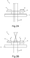
Figures 2A and 2B . In these figures, the optical device, designated by 10, comprises a deformable part ordiaphragm 15, for example of glass, resting, through a lens element 11 (made, for example, of polymeric material), on asupport 12, which is, for example, also of glass; thediaphragm 15 further carries twopiezoelectric regions 13, arranged a at a distance from each other. In the absence of a bias (Figure 2A ), thediaphragm 15 and thelens element 11 have a planar surface and do not modify the path of alight beam 16 that traverses them. When thepiezoelectric regions 13 are biased, they cause a deformation of thediaphragm 15. The deformation of the central area of thediaphragm 15 is transmitted to thelens element 11, the top surface whereof curves, modifying the focus of thelens element 11 and thus the path of the light beam 16 (Figure 2B ). It is thus possible to modify the characteristics of optical transmission of theoptical device 10. - The piezoelectric actuators illustrated in
Figures 1A, 1B ,2A, and 2B has the advantage of being fast and compact devices; in fact, unlike other types of actuators, such as capacitive and/or magnetic actuators, they do not require further structures, such as electrodes connected to a reference potential (as in the case of capacitive actuators) or magnets and/or coils (as in the case of magnetic actuators). - Another embodiment of piezoelectric-actuation MEMS device is illustrated in
Figure 3 and designated hereinafter by 30. In particular, theMEMS device 30 ofFigure 3 has a quadrangular shape (e.g., square) in top plan view, with a side having a length D and its centre O lying on a central axis C parallel to a first axis Z of a Cartesian reference system XYZ. - The
MEMS device 30 comprises asubstrate 32, of semiconductor material (e.g., silicon), having afirst surface 32A and asecond surface 32B. Thesubstrate 32 has acavity 34 extending from thesecond surface 32B. - In detail, the
cavity 34 is laterally delimited by a wall and at the top by abottom surface 32C. Thesubstrate portion 32 delimited between thebottom surface 32C of thecavity 34 and thefirst surface 32A of thesubstrate 32 forms adiaphragm 37, and is thus monolithic with thesubstrate 32. Thecavity 34 generally has, in top plan view, a quadrangular shape (e.g., square) and has an extension, along a second axis X of the Cartesian reference system XYZ, of a length L. The length L is further smaller than the diameter D of the device. - An
insulating layer 39, for example, of silicon oxide (SiO2), extends over thefirst surface 32A of thesubstrate 32, and astructural layer 41, for example, of polysilicon, oxide, or some other material, extends over theinsulating layer 39. - Extending on the
structural layer 41, all along the periphery of theMEMS device 30, is apiezoelectric actuator 50, which is annulus-shaped and is formed by a stack of layers. In particular, the stack of layers comprises afirst electrode 60; a layer ofpiezoelectric material 61, for example of PZT (Pb, Zr, TiO2), which extends over thefirst electrode 61; asecond electrode 62, which extends over the layer ofpiezoelectric material 61; and apassivation layer 63, which extends over thesecond electrode 62 and over the exposed surface of thestructural layer 41. Acontact electrode 64, of metal material (such as gold, aluminium, or copper) and, for example, annulus-shaped, extends on thepassivation layer 63 and is vertically aligned to thepiezoelectric actuator 50; further, thecontact electrode 64 is electrically connected to thesecond electrode 62 by acontact trench 64A, which extends at least in part through thepassivation layer 63. - Alternatively, the
MEMS device 30 may not have thecontact electrode 64 and have, on top and/or within thestructural layer 41, electrical interconnections for biasing thepiezoelectric actuator 50. - In use, a potential difference is applied between the first and
second electrodes piezoelectric actuator 50 to generate a deflection of thediaphragm 37 in an upward direction (i.e., along the first axis Z, towards the outside of the cavity 34) in a unidirectional way. - The piezoelectrically actuated devices illustrated in
Figures 1A, 1B ,2A, 2B and3 do not effectively block deformation of the mobile structures, here thediaphragm 37, in the presence of impact and mechanical stresses. - Further, for MEMS actuators, as the
MEMS device 30 illustrated inFigure 3 , optimization of the shapes may be limited. In fact, with the current processes, thediaphragm 37 is defined using an etching process for formation of thecavity 34, which determines the shape thereof. On the other hand, the optimal shape of thediaphragm 37 is dictated by its function, i.e., by the structures moved by thediaphragm 37 during actuation (e.g., mechanical transmission elements in pumps or speakers). It follows that it is difficult to reach a compromise between the functional requirements and the manufacturing processes currently used. - The aim of the present invention is to provide a MEMS device and a manufacturing process that overcome the drawbacks of the prior art.
- According to the present invention, a MEMS device and the manufacturing process thereof are provided, as defined in the attached claims.
- For a better understanding of the present invention, preferred embodiments thereof are now described, purely by way of non-limiting example, with reference to the attached drawings, wherein:
-
Figures 1A and 1B show simplified lateral views of a known piezoelectrically actuated MEMS actuator in a rest condition and a deformed condition, respectively; -
Figures 2A and 2B show simplified lateral views of another known piezoelectrically actuated MEMS actuator, used in an optical device in a rest condition and a deformed condition, respectively; -
Figure 3 is a simplified cross-sectional view of a known piezoelectrically actuated MEMS actuator; -
Figure 4 is a cross-sectional view of the present MEMS device according to an embodiment; -
Figures 5-11 are cross-sections of the MEMS device ofFigure 4 in successive manufacturing steps; -
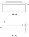
Figures 12 and 13 are cross-sections of the MEMS device ofFigure 4 in successive manufacturing steps of the buried cavity according to a variant of the manufacturing process; -
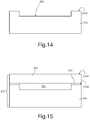
Figures 14 and 15 are cross-sections of the MEMS device ofFigure 4 in successive manufacturing steps of the buried cavity, according to another variant of the manufacturing process; -
Figures 16A-16F are top plan views, with parts in ghost view and portions removed, of different embodiments of the present MEMS device; and -
Figure 17 is a block diagram of an electronic apparatus including the MEMS device ofFigure 16 . -
Figures 4 and16A show an embodiment of a piezoelectrically actuatedMEMS device 70; in particular, without this implying any loss of generality, theMEMS device 70 is an actuator for mechanical applications, such as valves and pistons, or for optical applications. - The
MEMS device 70 ofFigures 4 and16A has a parallelepipedal shape, with a length D, in a direction parallel to a first axis X of a Cartesian reference system XYZ, and comprises apiezoelectric actuator 90, having the shape, for example, of an annulus with centre O lying on a central axis C parallel to a second axis Z of the Cartesian reference system XYZ. - The
MEMS device 70 comprises abody 72, having afirst surface 72A and asecond surface 72B. Thebody 72 comprises asubstrate 73, of semiconductor material, such as silicon; an insulatinglayer 79, for example, of silicon oxide (SiO2), extending over thesubstrate 73; and astructural layer 81, for example, of polysilicon, oxide, or other material compatible with semiconductor technology. - The
substrate 73 has adiaphragm cavity 74 extending from thesecond surface 72B and through thesubstrate 73 in the direction of the thickness of thesubstrate 73; thediaphragm cavity 74 is closed at the top by the insulatinglayer 79, which forms abottom surface 74A of thediaphragm cavity 74. - The
diaphragm cavity 74 is laterally delimited by awall 74B and has a quadrangular shape in bottom plane view. In particular, inFigure 4 , thediaphragm cavity 74 has a base with a square shape with side of length L (see alsoFigure 16A ). - A
recess 78 of an annular shape laterally extends in thebody 72 from thediaphragm cavity 74, at a short distance from the insulatinglayer 79. In a bottom plane view, therecess 78 here is ring-shaped with maximum diameter D', greater than the length L, and is concentric to thediaphragm cavity 74. - The
structural layer 81 is delimited at the top by thefirst surface 72A of thebody 72 and forms, at thebottom surface 72A of thediaphragm cavity 74, adeformable portion 77. - The
substrate 73 further includes aflexible stopper portion 72C extending between thedeformable portion 77 and therecess 78. - The
piezoelectric actuator 90 extends on thefirst surface 72A of thebody 72 and comprises afirst electrode 100; apiezoelectric region 101, for example, of PZT (Pb, Zr, TiO2), which extends over thefirst electrode 101; and asecond electrode 102, which extends over thepiezoelectric region 101. - A
passivation layer 103, for example, of silicon oxide or silicon nitride (Si3N4), extends over thesecond electrode 102 and on thefirst surface 72A, where the latter is exposed, entirely coating thepiezoelectric actuator 90 and thestructural layer 81. Acontact region 104, for example of metal (such as gold or aluminium), extends on thepassivation layer 103 and is electrically coupled to a bias and control electronics (not illustrated). In particular, thecontact region 104 is arranged to be vertically aligned to thepiezoelectric actuator 90. Further, thecontact region 104 is electrically coupled to thesecond electrode 102 by acontact trench 104A dug in thepassivation layer 103. - Alternatively, the
MEMS device 70 may not have acontact region 104 but, on and/or within thestructural layer 81, electrical interconnections (not illustrated) for biasing thepiezoelectric actuator 90. - In use, a potential difference is applied between the first and
second electrodes piezoelectric actuator 90 to generate a deflection of thedeformable portion 77 in a direction parallel to the first axis Z, in a per se known manner. This deflection enables theMEMS device 70 to operate according to the desired technical effect. - In greater detail, the
flexible stopper portion 72C is able to bend when thedeformable portion 77 undergoes an high deformation (e.g., due to a fall). - For instance, if a high force is applied on the
bottom surface 74A of thediaphragm cavity 74, thedeformable portion 77 moves away from the diaphragm cavity 74 (i.e., in a direction parallel to the second axis Z). Such force is also applied to theflexible stopper portion 72C, which bends in the same direction as thedeformable portion 77; in this way, theflexible stopper portion 72C is able to absorb part of the force applied to thebottom surface 74A and, thus, to thedeformable portion 77, reducing the impact of the force on theMEMS device 70. - This deflection enables, for example, opening or closing (in the case of its application as a valve) or executing a vertical movement (in applications such as pistons or speakers).
-
Figures 5-11 illustrate successive manufacturing steps of theMEMS device 70 ofFigure 4 , according to a first embodiment. - Initially,
Figure 5 , in a wafer 73' of monocrystalline semiconductor material such as silicon, a buried cavity, intended to form therecess 78, is formed. For instance, for this purpose, the manufacturing process described in the European patentEP 1577656 (corresponding to the patentUS 8173513 ) and summarised below may be used. - In detail,
Figure 5 , using a resist mask (not illustrated) having honeycomb-lattice openings, an anisotropic chemical etch is carried out on a firsttop surface 73A' of the wafer 73' so as to form a plurality oftrenches 120, which communicate with one another and delimit a plurality ofcolumns 121 of silicon. In particular, the plurality oftrenches 120 is formed in an area of thesubstrate 73 where therecess 78 is to be formed. - Next, after removing the mask (not illustrated), an epitaxial growth is carried out in a reducing environment. Consequently, an epitaxial layer grows on the first
top surface 73A' of the wafer 73', closing thetrenches 120 at the top. - A thermal annealing step is then carried out, for example for 30 minutes at 1190°C, preferably in a hydrogen, or, alternatively, nitrogen atmosphere. As discussed in the patents referred to above, the annealing step causes a migration of the silicon atoms, which tend to move into a position of lower energy. Consequently (
Figure 6 ), and also by virtue of the short distance between thecolumns 121, the silicon atoms of the latter migrate completely, and a buriedcavity 76 is formed. A thin silicon layer, for example having a thickness comprised between 5 µm and 10 µm (e.g., 6 µm), remains on top of the buriedcavity 76 and is formed in part by epitaxially grown silicon atoms and in part by migrated silicon atoms. Awafer 73" is thus obtained, having a secondtop surface 73A" and a bottom surface, the latter corresponding to thesecond surface 72B of thebody 72 and thus being designated by the same reference number. - Next (
Figure 7 ), the insulatinglayer 79 is deposited on the secondtop surface 73A" of thewafer 73", according to known techniques. For instance, the insulatinglayer 79 has a thickness comprised between 0.5 µm and 1.5 µm. - With reference to
Figure 8 , thestructural layer 81, of polycrystalline silicon or of an optically transparent material, is deposited on the insulatinglayer 79. In particular, thestructural layer 81 has a thickness, for example, comprised between 3 µm and 25 µm and has a top surface, which corresponds to thefirst surface 72A of thebody 72 and is thus designated by the same reference number inFigure 8 . - Next (
Figure 9 ), thefirst electrode 100 is formed on thefirst surface 72A of thebody 72 using known deposition and masking techniques. Then, a piezoelectric layer and an electrode layer are deposited in succession and defined using known masking and definition techniques so as to form thepiezoelectric region 101 and thesecond electrode 102. - Next (
Figure 10 ), thepassivation layer 103 is deposited on thesecond electrode 102 and on thefirst surface 72A, coating thestructural layer 81 and thepiezoelectric actuator 90 completely. Then, thecontact region 104 is formed on thepassivation layer 103, which has previously been etched to form the via 104A. - In
Figure 11 , amask layer 125 is deposited and patterned on thesecond surface 72B of thewafer 73", which is etched from the back using known photolithographic and etching techniques (e.g., anisotropic chemical etching such as DRIE - Deep Reactive Ion Etching), so as to form thediaphragm cavity 74. In particular, the etching step is carried out until the buriedcavity 76 is reached, as far as the insulatinglayer 79, and so that thediaphragm cavity 74 is concentric to the buriedcavity 76. In practice, thediaphragm cavity 74 passes right through thewafer 73" and incorporates most of the buriedcavity 76 to release thedeformable portion 77; at the end, of the buriedcavity 76 only therecess 78 remains to be separately visible. - At the end of the process, the
mask layer 125 is removed, thewafer 73" is diced, and theMEMS device 70 ofFigure 4 is thus obtained. - The buried
cavity 76 of thewafer 73" may also be formed in a different way. For instance,Figures 12-13 show a solution wherein the buriedcavity 76 is obtained by removing a sacrificial layer. In these figures, elements in common withFigures 5-11 are designated by the same reference numbers increased by 200. - In
Figure 12 , a sacrificial layer, for example, of silicon oxide, is deposited on thetop surface 273A' of the wafer 273' and is then patterned so as to form asacrificial region 230 having a shape complementary to the buriedcavity 76 ofFigure 6 . In particular, thesacrificial region 230 has a cylindrical shape of diameter D' and a thickness T (defined in a direction parallel to the second axis Z). - Next (
Figure 13 ), a covering layer, here designated by thereference number 231, for example, of polysilicon, is grown on thesacrificial layer 230 according to growth techniques per se known, to obtain thewafer 273". - The further manufacturing steps are similar to the ones described in
Figures 7-11 . In particular, here two etches are carried out, initially comprising etching thewafer 273" to form a first portion of thediaphragm cavity 74 ofFigure 4 and then etching thesacrificial layer 230, which is removed so as to obtain theinner cavity 76 ofFigure 6 . Then, an etch is carried out on thecovering layer 231 so as to release completely thedeformable portion 77 and thus obtain theMEMS device 70 ofFigure 4 . -
Figures 14-15 show a further solution for forming the buriedcavity 76 ofFigure 6 , here designated by the reference number 378. In particular, elements that are in common with the ones described with reference toFigures 5-11 are designated inFigures 14-15 by the same reference numbers increased by 300. - In detail,
Figure 14 , a first wafer 373' is selectively etched, by masking and etching techniques per se known, from itstop surface 373A' so as to obtain agroove 335 having a circular shape in top plan view and dimensions substantially equal to those of the buriedcavity 76 ofFigure 6 . - Then,
Figure 15 , a coveringwafer 345 is bonded to the first wafer 373' by a bonding layer 340 (for example, of oxide, polymer, or metal). The coveringwafer 345 thus closes thegroove 335 at the top to form a buriedcavity 376 corresponding to the buriedcavity 76 ofFigure 6 . - Manufacturing steps similar to the ones described with reference to
Figures 6-11 then follow. -
Figures 16A-16F show different shapes of therecess 78 and/or of theactuator 90 of theMEMS device 70 ofFigure 4 , irrespective of whether therecess 78 is obtained according toFigures 5-6 orFigures 12-16 . In particular, inFigures 16A-16F , for a clearer understanding, thepassivation layer 103 and thecontact electrodes 104 ofFigure 4 have been removed. - In the top plan view of
Figure 16A (as already mentioned), thepiezoelectric actuator 90 is annulus-shaped, therecess 78 is ring-shaped, and thediaphragm cavity 74 is square-shaped. Therecess 78 and thediaphragm cavity 74 are concentric to each other. Further, therecess 78 has a diameter D' smaller than the outer diameter, here designated by Dm, of thepiezoelectric actuator 90 and approximately equal to the diagonal of thediaphragm cavity 74. - In
Figure 16B , thepiezoelectric actuator 90 has a full circular shape, therecess 78 also has a circular shape, and thediaphragm cavity 74 has a square shape. As may be noted in the top plan view ofFigure 16B , thepiezoelectric actuator 90 has an area larger than thediaphragm cavity 74 and completely surrounds it. This embodiment may be advantageously used in devices that, in use, perform vertical movements (i.e., along the first axis Z), such as pistons, switches, or speakers. - In
Figure 16C , thepiezoelectric actuator 90 is annulus-shaped in top plan view; further, therecess 78 here is annulus shaped (obtained from a ring-shaped buried cavity 76), and thediaphragm cavity 74 is square-shaped. In particular, therecess 78 has an outer diameter D' smaller than the outer diameter Dm of thepiezoelectric actuator 90 and an inner diameter approximately equal to the side L of thediaphragm cavity 74. As inFigure 16A , thepiezoelectric actuator 90 exposes the central area of theunderlying body 72 so that, in use, the device may be used for applications such as a piston. - In
Figure 16D , therecess 78 has the shape of an annulus in top plan view (obtained from a buriedcavity 76 of an annular shape), thediaphragm cavity 74 has a square shape, and thepiezoelectric actuator 90 is formed by a plurality ofactuator elements 90A (eight inFigure 16D ), having the same layered structure as thepiezoelectric actuator 90 ofFigure 4 respectively. In detail, eachactuator element 90A has a quadrangular shape (e.g., rectangular) in top plan view; theactuator elements 90A are arranged radially and at a uniform angular distance from the centre O. For instance, in the embodiment considered, eachactuator element 90A is arranged at 45° from theadjacent actuator elements 90A. This embodiment may, for example, be advantageously used for applications in which thedevice 70 is required to perform movements both horizontally and vertically, for example, for compensating possible contact problems (e.g., in pistons) or of closing (e.g., in valves). - In
Figure 16E , in top plan view, therecess 78 has the shape of an annulus (obtained from a buriedcavity 76 of an annular shape), and thepiezoelectric actuator 90 has a full circular shape; thediaphragm cavity 74 has a square shape. In particular, therecess 78 has an outer diameter D' smaller than the outer diameter Dm of thepiezoelectric actuator 90 and an inner diameter approximately equal to the side L of thediaphragm cavity 74. In this way, thepiezoelectric actuator 90 extends completely over thediaphragm cavity 74. The embodiment ofFigure 16E is used in the case where theMEMS device 70 is required, for example, to perform vertical movements (i.e., along the first axis Z) in applications such as valves or pistons. - In
Figure 16F , thepiezoelectric actuator 90 has the shape of an annulus in top plan view. Thediaphragm cavity 74 is formed by a plurality ofcavity parts 78A (eight inFigure 16F ) arranged at a same distance from the centre O. In detail, eachcavity part 78A has a quadrangular shape (e.g., rectangular) in top plan view and is arranged radially and at a uniform angular distance from theadjacent cavity parts 78A. For instance, in the embodiment ofFigure 16F , eachcavity part 78A is arranged at 45° from theadjacent cavity parts 78A. This embodiment thus has lateral recesses, which may be used, for example, as stoppers. -
Figure 17 shows anelectronic device 700 that uses, for example, theMEMS device 70 ofFigure 4 . - The
electronic device 700 comprises, in addition to theMEMS device 70, a microprocessor (CPU) 701, amemory block 702, connected to themicroprocessor 701, and an input/output interface 703, for example a keypad and/or a display, which is also connected to themicroprocessor 701. AnASIC 704 may be integrated in theMEMS device 70 or, as illustrated inFigure 17 , be arranged outside theMEMS device 70 and operatively coupled thereto. - The
MEMS device 70 communicates with themicroprocessor 701 via theASIC 704. - The
electronic device 700 is, for example, a mobile communication device, such as a mobile phone or a smartphone, a PDA, or a computer, but may also be a voice recorder, an audio-file player with voice-recording capacity, a console for video games, and the like. - The advantages of the MEMS device described emerge clearly from the foregoing description.
- In particular, the
recess 78 and theflexible stopper portion 72C form a stopping structure or a lateral mechanical stopper structure that limits deformation of thedeformable portion 77 and thus its deflection in the direction of thediaphragm cavity 74 in the presence of possible mechanical shocks, e.g. falls. - Finally, it is clear that modifications and variations may be made to the device and to the method described and illustrated herein, without thereby departing from the scope of the present invention, as defined in the attached claims.
- For instance, the various embodiments described may be combined to provide further solutions. In particular, the piezoelectric actuator and/or the diaphragm cavity may have a different shape, for example a regular polygonal shape.
- Further, the
structural layer 81 of theMEMS device 70 ofFigure 4 may be of BPSG (BoroPhosphoSilicate Glass) or other transparent materials (such as oxides); further, thepassivation layer 103 may be defined simultaneously with thecontact electrode 104 so as to expose the central portion of thestructural layer 81. Such modifications enable use of theMEMS device 70 for instance for optical applications, such as auto-focus, retaining all the advantages listed previously.
Claims (14)
- A MEMS device (70) comprising:a body (72), having a thickness in a thickness direction, a first surface (72A) and a second surface (72B);a diaphragm cavity (74) in the body, extending in the direction of thickness of the body from the second surface;a deformable portion (77) in the body between the first surface and the diaphragm cavity;a piezoelectric actuator (90), extending over the first surface of the body, on the deformable portion; anda recess structure (78) extending in the body from the diaphragm cavity in a transverse direction to the thickness direction of the body and delimiting, in the body, a flexible stopper portion (72C) for the deformable portion, the flexible stopper portion being disposed between the deformable portion and the recess structure.
- The device according to claim 1, wherein the body comprises a substrate (73) of semiconductor material having a thickness, and a structural layer (81), the structural layer extending over the substrate and defining the first surface (72A), the deformable portion (77) being formed in the structural layer, and the diaphragm cavity (74) extending throughout the thickness of the substrate.
- The device according to any of the preceding claims, wherein, in a transverse plane to the direction of thickness of the body (72), the diaphragm cavity (74) has a quadrangular shape, and the recess structure (78) is formed selectively by a ring-shaped recess (78), a polygonally-shaped recess (78), a plurality of radially extending parts.
- The device according to claim 3, wherein the radially extending parts extend at an angular distance of 45° from each other.
- The device according to any of the preceding claims, wherein the piezoelectric actuator (90) is formed selectively by a region of a cylindrical shape, a region of a hollow cylindrical shape, a region of a parallelepipedal shape, a plurality of adjacent actuator elements, extending radially and angularly spaced.
- The device according to claim 5, wherein the piezoelectric actuators (90A) extend angularly spaced by 45° from each other.
- The device according to any of the previous claims, wherein the diaphragm cavity (74) and the recess structure (78) are concentric.
- The device according to any of the previous claims, wherein the flexible stopper portion (72C) is configured to bend when a force higher than a threshold is applied to the deformable portion (77).
- An electronic apparatus (700) comprising:- the MEMS device (70) according to any of claims 1-8;- an ASIC (704) communicating with the MEMS device;- a memory block (702);- an input/output interface (703); and- a microprocessor (701), communicating with the ASIC, the memory block, and the input/output interface.
- A method for manufacturing a MEMS device (70), comprising:forming a recess-delimitation structure (76; 230; 376) within a body (72) having a thickness in a thickness direction;forming a piezoelectric actuator (90), on a first surface of the body (72A);removing selective portions in the body from a second surface (72B) of the body to form a diaphragm cavity (74) extending in the thickness of the body up to the recess-delimitation structure, the diaphragm cavity delimiting a deformable portion (77) of the body arranged between the first surface and the diaphragm cavity,wherein the recess-delimitation structure is patterned to form, after removing selective portions in the body, a recess structure (78) extending in the body underneath the first surface from the cavity in a transverse direction to the thickness direction of the body and forming, in the body, a flexible stopper portion (72C) for the deformable portion, the flexible stopper portion being disposed between the deformable portion and the recess structure.
- The method according to claim 10, wherein forming the recess-delimitation structure comprises forming a buried cavity (76; 230; 376).
- The method according to claim 11, wherein forming the buried cavity (76) comprises:forming, within a first wafer (73') of monocrystalline semiconductor material, trenches (120) extending from a face of the first wafer and delimiting between each other columns (121) of semiconductor material;epitaxially growing, from the columns (121), a closing layer of semiconductor material, enclosing the buried cavity (76), the closing layer closing the trenches at the top; andcarrying out a thermal annealing and causing migration of the semiconductor material of the columns towards the closing layer.
- The method according to claim 11, wherein forming the buried cavity comprises:forming a groove (335) within a first wafer (373'); andbonding the first wafer to a covering wafer (345).
- The method according to claim 11, wherein forming the recess-delimitation structure comprises: forming a sacrificial region (230) on a first wafer (273'); and forming a covering layer (231) extending on and adjacent to the sacrificial region,
and wherein removing selective portions in the body comprises removing the sacrificial layer.
Applications Claiming Priority (1)
| Application Number | Priority Date | Filing Date | Title |
|---|---|---|---|
| IT102017000124348A IT201700124348A1 (en) | 2017-10-31 | 2017-10-31 | MEMIE DEVICE OF PIEZOELECTRIC TYPE WITH SUSPENDED MEMBRANE AND ITS MANUFACTURING PROCESS |
Publications (2)
| Publication Number | Publication Date |
|---|---|
| EP3477715A1 true EP3477715A1 (en) | 2019-05-01 |
| EP3477715B1 EP3477715B1 (en) | 2024-07-24 |
Family
ID=61187748
Family Applications (1)
| Application Number | Title | Priority Date | Filing Date |
|---|---|---|---|
| EP18203888.5A Active EP3477715B1 (en) | 2017-10-31 | 2018-10-31 | Piezoelectric mems device having a suspended diaphragm and manufacturing process thereof |
Country Status (4)
| Country | Link |
|---|---|
| US (1) | US11427463B2 (en) |
| EP (1) | EP3477715B1 (en) |
| CN (2) | CN109721022B (en) |
| IT (1) | IT201700124348A1 (en) |
Families Citing this family (9)
| Publication number | Priority date | Publication date | Assignee | Title |
|---|---|---|---|---|
| IT201700124348A1 (en) * | 2017-10-31 | 2019-05-01 | St Microelectronics Srl | MEMIE DEVICE OF PIEZOELECTRIC TYPE WITH SUSPENDED MEMBRANE AND ITS MANUFACTURING PROCESS |
| US11970391B2 (en) | 2019-12-13 | 2024-04-30 | Shenzhen Institutes Of Advanced Technology | Flexible electrode and preparation method thereof |
| CN111017870B (en) * | 2019-12-13 | 2023-08-08 | 深圳市中科先见医疗科技有限公司 | Flexible electrode and preparation method thereof |
| IT202000010264A1 (en) * | 2020-05-07 | 2021-11-07 | St Microelectronics Srl | PIEZOELECTRIC ACTUATOR HAVING A DEFORMATION SENSOR AND RELATED MANUFACTURING PROCEDURE |
| US12438516B2 (en) | 2021-03-22 | 2025-10-07 | Agency For Science, Technology And Research | Resonator and method of forming the same |
| DE102021205485A1 (en) * | 2021-05-28 | 2022-12-01 | Robert Bosch Gesellschaft mit beschränkter Haftung | Process for the production of a micro-electronic-mechanical vibration system and piezoelectric micro-manufactured ultrasonic transducer |
| US12515942B2 (en) | 2021-06-25 | 2026-01-06 | Stmicroelectronics S.R.L. | MEMS device comprising an insulated suspended diaphragm, in particular pressure sensor, and manufacturing process thereof |
| US12238478B2 (en) | 2022-01-18 | 2025-02-25 | Taiwan Semiconductor Manufacturing Company, Ltd. | Top notch slit profile for MEMS device |
| WO2023146962A2 (en) | 2022-01-26 | 2023-08-03 | Cornell University | Artificial cilium and arrays thereof |
Citations (9)
| Publication number | Priority date | Publication date | Assignee | Title |
|---|---|---|---|---|
| EP1577656A1 (en) | 2004-03-19 | 2005-09-21 | STMicroelectronics S.r.l. | Method for manufacturing a semiconductor pressure sensor |
| WO2006134580A2 (en) * | 2005-06-17 | 2006-12-21 | Kolo Technologies, Inc. | Micro-electro-mechanical transducer having an insulation extension |
| US20090109262A1 (en) * | 2007-10-30 | 2009-04-30 | Cruz-Uribe Tony S | Fluid ejection device |
| EP2270892A1 (en) * | 2008-04-18 | 2011-01-05 | NGK Insulators, Ltd. | Method for testing piezoelectric/electrostrictive device, testing apparatus, and method for adjusting piezoelectric/electrostrictive device |
| US20130130502A1 (en) * | 2010-05-21 | 2013-05-23 | Sand 9, Inc. | Micromechanical membranes and related structures and methods |
| US20150021734A1 (en) * | 2013-07-18 | 2015-01-22 | Infineon Technologies Dresden Gmbh | Semiconductor device, a micro-electro-mechanical resonator and a method for manufacturing a semiconductor device |
| US20150145374A1 (en) * | 2013-11-26 | 2015-05-28 | Agency For Science, Technology And Research | Transducer and method for forming the same |
| WO2016007250A1 (en) * | 2014-07-08 | 2016-01-14 | Qualcomm Incorporated | Piezoelectric ultrasonic transducer and process |
| US20160027988A1 (en) * | 2014-07-28 | 2016-01-28 | Rohm Co., Ltd. | Piezoelectric membrane, piezoelectric device, and inkjet head |
Family Cites Families (9)
| Publication number | Priority date | Publication date | Assignee | Title |
|---|---|---|---|---|
| JP3875240B2 (en) * | 2004-03-31 | 2007-01-31 | 株式会社東芝 | Manufacturing method of electronic parts |
| JP4144640B2 (en) * | 2006-10-13 | 2008-09-03 | オムロン株式会社 | Method for manufacturing vibration sensor |
| JP2010199133A (en) * | 2009-02-23 | 2010-09-09 | Yamaha Corp | Method of manufacturing mems, and mems |
| US8633553B2 (en) * | 2010-07-26 | 2014-01-21 | Stmicroelectronics S.R.L. | Process for manufacturing a micromechanical structure having a buried area provided with a filter |
| JP6028479B2 (en) * | 2012-09-14 | 2016-11-16 | オムロン株式会社 | Capacitive sensor, acoustic sensor and microphone |
| US9102519B2 (en) * | 2013-03-14 | 2015-08-11 | Infineon Technologies Ag | Semiconductor devices and methods of forming thereof |
| IT201700124348A1 (en) * | 2017-10-31 | 2019-05-01 | St Microelectronics Srl | MEMIE DEVICE OF PIEZOELECTRIC TYPE WITH SUSPENDED MEMBRANE AND ITS MANUFACTURING PROCESS |
| DE102020108433B4 (en) * | 2020-03-26 | 2023-05-04 | Tdk Corporation | Device with a membrane and method of manufacture |
| US11498097B2 (en) * | 2020-05-21 | 2022-11-15 | Vanguard International Semiconductor Corporation | Piezoelectric micromachined ultrasonic transducer and method of fabricating the same |
-
2017
- 2017-10-31 IT IT102017000124348A patent/IT201700124348A1/en unknown
-
2018
- 2018-10-19 US US16/165,828 patent/US11427463B2/en active Active
- 2018-10-30 CN CN201811280031.1A patent/CN109721022B/en active Active
- 2018-10-30 CN CN201821772595.2U patent/CN209367796U/en active Active
- 2018-10-31 EP EP18203888.5A patent/EP3477715B1/en active Active
Patent Citations (10)
| Publication number | Priority date | Publication date | Assignee | Title |
|---|---|---|---|---|
| EP1577656A1 (en) | 2004-03-19 | 2005-09-21 | STMicroelectronics S.r.l. | Method for manufacturing a semiconductor pressure sensor |
| US8173513B2 (en) | 2004-03-19 | 2012-05-08 | Stmicroelectronics S.R.L. | Method for manufacturing a semiconductor pressure sensor |
| WO2006134580A2 (en) * | 2005-06-17 | 2006-12-21 | Kolo Technologies, Inc. | Micro-electro-mechanical transducer having an insulation extension |
| US20090109262A1 (en) * | 2007-10-30 | 2009-04-30 | Cruz-Uribe Tony S | Fluid ejection device |
| EP2270892A1 (en) * | 2008-04-18 | 2011-01-05 | NGK Insulators, Ltd. | Method for testing piezoelectric/electrostrictive device, testing apparatus, and method for adjusting piezoelectric/electrostrictive device |
| US20130130502A1 (en) * | 2010-05-21 | 2013-05-23 | Sand 9, Inc. | Micromechanical membranes and related structures and methods |
| US20150021734A1 (en) * | 2013-07-18 | 2015-01-22 | Infineon Technologies Dresden Gmbh | Semiconductor device, a micro-electro-mechanical resonator and a method for manufacturing a semiconductor device |
| US20150145374A1 (en) * | 2013-11-26 | 2015-05-28 | Agency For Science, Technology And Research | Transducer and method for forming the same |
| WO2016007250A1 (en) * | 2014-07-08 | 2016-01-14 | Qualcomm Incorporated | Piezoelectric ultrasonic transducer and process |
| US20160027988A1 (en) * | 2014-07-28 | 2016-01-28 | Rohm Co., Ltd. | Piezoelectric membrane, piezoelectric device, and inkjet head |
Also Published As
| Publication number | Publication date |
|---|---|
| CN109721022A (en) | 2019-05-07 |
| CN209367796U (en) | 2019-09-10 |
| CN109721022B (en) | 2024-03-19 |
| IT201700124348A1 (en) | 2019-05-01 |
| US20190127214A1 (en) | 2019-05-02 |
| US11427463B2 (en) | 2022-08-30 |
| EP3477715B1 (en) | 2024-07-24 |
Similar Documents
| Publication | Publication Date | Title |
|---|---|---|
| EP3477715B1 (en) | Piezoelectric mems device having a suspended diaphragm and manufacturing process thereof | |
| CN110392331B (en) | Piezoelectric MEMS transducer and method of manufacturing the same | |
| US12185633B2 (en) | Piezoelectric mems device with a suspended membrane having high mechanical shock resistance and manufacturing process thereof | |
| US20230204974A1 (en) | Piezoelectric mems actuator for compensating unwanted movements and manufacturing process thereof | |
| KR101910867B1 (en) | System and method for a differential comb drive mems | |
| KR101710334B1 (en) | Device comprising a deflectable structure | |
| EP3809476A1 (en) | Transducer with improved piezoelectric arrangement, mems device comprising the transducer, and methods for manufacturing the transducer | |
| US8174083B1 (en) | Dual-suspension system for MEMS-based devices | |
| CN108249388B (en) | Piezoelectric microelectromechanical actuator device movable in a plane | |
| EP3705451B1 (en) | Mems structure including a cap with a via | |
| CN113620232A (en) | Piezoelectric actuator with deformable structure having improved mechanical properties and method for manufacturing same | |
| US20020126455A1 (en) | Tiled microelectromechanical device modules and fabrication methods | |
| US11818957B2 (en) | Piezoelectrically actuated MEMS optical device having a protected chamber and manufacturing process thereof | |
| CN218841706U (en) | Self-aligned polycrystalline silicon and monocrystalline silicon hybrid MEMS vertical comb electrode | |
| CN115784143B (en) | Self-aligned polycrystalline silicon single crystal silicon hybrid MEMS vertical electrode and manufacturing method thereof | |
| JP3871118B2 (en) | Microdevice manufacturing method | |
| KR100400742B1 (en) | piezoelectric type micro mirror and method for fabricating the same | |
| US20250175098A1 (en) | Piezoelectric mems device, in particular micro-actuator, and manufacturing process thereof | |
| CN110366083B (en) | MEMS device and preparation method thereof | |
| GB2375185A (en) | Thick wafer for MEMS fabrication | |
| JP2010145268A (en) | Method for manufacturing mems sensor, and mems | |
| JPH05259477A (en) | Minute mobile machine and manufacture thereof | |
| HK1161362A (en) | Mems device |
Legal Events
| Date | Code | Title | Description |
|---|---|---|---|
| PUAI | Public reference made under article 153(3) epc to a published international application that has entered the european phase |
Free format text: ORIGINAL CODE: 0009012 |
|
| STAA | Information on the status of an ep patent application or granted ep patent |
Free format text: STATUS: THE APPLICATION HAS BEEN PUBLISHED |
|
| AK | Designated contracting states |
Kind code of ref document: A1 Designated state(s): AL AT BE BG CH CY CZ DE DK EE ES FI FR GB GR HR HU IE IS IT LI LT LU LV MC MK MT NL NO PL PT RO RS SE SI SK SM TR |
|
| AX | Request for extension of the european patent |
Extension state: BA ME |
|
| STAA | Information on the status of an ep patent application or granted ep patent |
Free format text: STATUS: REQUEST FOR EXAMINATION WAS MADE |
|
| 17P | Request for examination filed |
Effective date: 20191029 |
|
| RBV | Designated contracting states (corrected) |
Designated state(s): AL AT BE BG CH CY CZ DE DK EE ES FI FR GB GR HR HU IE IS IT LI LT LU LV MC MK MT NL NO PL PT RO RS SE SI SK SM TR |
|
| STAA | Information on the status of an ep patent application or granted ep patent |
Free format text: STATUS: EXAMINATION IS IN PROGRESS |
|
| 17Q | First examination report despatched |
Effective date: 20210419 |
|
| REG | Reference to a national code |
Ref legal event code: R079 Ipc: H10N0030010000 Ref country code: DE Ref legal event code: R079 Ref document number: 602018072109 Country of ref document: DE Free format text: PREVIOUS MAIN CLASS: H01L0041090000 Ipc: H10N0030010000 |
|
| RIC1 | Information provided on ipc code assigned before grant |
Ipc: H03H 3/007 20060101ALN20231019BHEP Ipc: G02B 26/08 20060101ALI20231019BHEP Ipc: G02B 3/14 20060101ALI20231019BHEP Ipc: B81B 3/00 20060101ALI20231019BHEP Ipc: H10N 30/20 20230101ALI20231019BHEP Ipc: H10N 30/01 20230101AFI20231019BHEP |
|
| GRAP | Despatch of communication of intention to grant a patent |
Free format text: ORIGINAL CODE: EPIDOSNIGR1 |
|
| STAA | Information on the status of an ep patent application or granted ep patent |
Free format text: STATUS: GRANT OF PATENT IS INTENDED |
|
| INTG | Intention to grant announced |
Effective date: 20231201 |
|
| RIC1 | Information provided on ipc code assigned before grant |
Ipc: H03H 3/007 20060101ALN20231120BHEP Ipc: G02B 26/08 20060101ALI20231120BHEP Ipc: G02B 3/14 20060101ALI20231120BHEP Ipc: B81B 3/00 20060101ALI20231120BHEP Ipc: H10N 30/20 20230101ALI20231120BHEP Ipc: H10N 30/01 20230101AFI20231120BHEP |
|
| RIN1 | Information on inventor provided before grant (corrected) |
Inventor name: PICCO, ANDREA Inventor name: FERRERA, MARCO Inventor name: PACI, DARIO |
|
| GRAJ | Information related to disapproval of communication of intention to grant by the applicant or resumption of examination proceedings by the epo deleted |
Free format text: ORIGINAL CODE: EPIDOSDIGR1 |
|
| STAA | Information on the status of an ep patent application or granted ep patent |
Free format text: STATUS: EXAMINATION IS IN PROGRESS |
|
| INTC | Intention to grant announced (deleted) | ||
| GRAP | Despatch of communication of intention to grant a patent |
Free format text: ORIGINAL CODE: EPIDOSNIGR1 |
|
| STAA | Information on the status of an ep patent application or granted ep patent |
Free format text: STATUS: GRANT OF PATENT IS INTENDED |
|
| RIC1 | Information provided on ipc code assigned before grant |
Ipc: H03H 3/007 20060101ALN20240315BHEP Ipc: G02B 26/08 20060101ALI20240315BHEP Ipc: G02B 3/14 20060101ALI20240315BHEP Ipc: B81B 3/00 20060101ALI20240315BHEP Ipc: H10N 30/20 20230101ALI20240315BHEP Ipc: H10N 30/01 20230101AFI20240315BHEP |
|
| INTG | Intention to grant announced |
Effective date: 20240419 |
|
| GRAS | Grant fee paid |
Free format text: ORIGINAL CODE: EPIDOSNIGR3 |
|
| GRAA | (expected) grant |
Free format text: ORIGINAL CODE: 0009210 |
|
| STAA | Information on the status of an ep patent application or granted ep patent |
Free format text: STATUS: THE PATENT HAS BEEN GRANTED |
|
| AK | Designated contracting states |
Kind code of ref document: B1 Designated state(s): AL AT BE BG CH CY CZ DE DK EE ES FI FR GB GR HR HU IE IS IT LI LT LU LV MC MK MT NL NO PL PT RO RS SE SI SK SM TR |
|
| REG | Reference to a national code |
Ref country code: GB Ref legal event code: FG4D |
|
| REG | Reference to a national code |
Ref country code: CH Ref legal event code: EP |
|
| REG | Reference to a national code |
Ref country code: DE Ref legal event code: R096 Ref document number: 602018072109 Country of ref document: DE |
|
| REG | Reference to a national code |
Ref country code: IE Ref legal event code: FG4D |
|
| REG | Reference to a national code |
Ref country code: LT Ref legal event code: MG9D |
|
| REG | Reference to a national code |
Ref country code: NL Ref legal event code: MP Effective date: 20240724 |
|
| PG25 | Lapsed in a contracting state [announced via postgrant information from national office to epo] |
Ref country code: PT Free format text: LAPSE BECAUSE OF FAILURE TO SUBMIT A TRANSLATION OF THE DESCRIPTION OR TO PAY THE FEE WITHIN THE PRESCRIBED TIME-LIMIT Effective date: 20241125 |
|
| REG | Reference to a national code |
Ref country code: AT Ref legal event code: MK05 Ref document number: 1707515 Country of ref document: AT Kind code of ref document: T Effective date: 20240724 |
|
| PG25 | Lapsed in a contracting state [announced via postgrant information from national office to epo] |
Ref country code: NL Free format text: LAPSE BECAUSE OF FAILURE TO SUBMIT A TRANSLATION OF THE DESCRIPTION OR TO PAY THE FEE WITHIN THE PRESCRIBED TIME-LIMIT Effective date: 20240724 |
|
| PG25 | Lapsed in a contracting state [announced via postgrant information from national office to epo] |
Ref country code: PT Free format text: LAPSE BECAUSE OF FAILURE TO SUBMIT A TRANSLATION OF THE DESCRIPTION OR TO PAY THE FEE WITHIN THE PRESCRIBED TIME-LIMIT Effective date: 20241125 Ref country code: NL Free format text: LAPSE BECAUSE OF FAILURE TO SUBMIT A TRANSLATION OF THE DESCRIPTION OR TO PAY THE FEE WITHIN THE PRESCRIBED TIME-LIMIT Effective date: 20240724 |
|
| PG25 | Lapsed in a contracting state [announced via postgrant information from national office to epo] |
Ref country code: NO Free format text: LAPSE BECAUSE OF FAILURE TO SUBMIT A TRANSLATION OF THE DESCRIPTION OR TO PAY THE FEE WITHIN THE PRESCRIBED TIME-LIMIT Effective date: 20241024 |
|
| PG25 | Lapsed in a contracting state [announced via postgrant information from national office to epo] |
Ref country code: FI Free format text: LAPSE BECAUSE OF FAILURE TO SUBMIT A TRANSLATION OF THE DESCRIPTION OR TO PAY THE FEE WITHIN THE PRESCRIBED TIME-LIMIT Effective date: 20240724 Ref country code: GR Free format text: LAPSE BECAUSE OF FAILURE TO SUBMIT A TRANSLATION OF THE DESCRIPTION OR TO PAY THE FEE WITHIN THE PRESCRIBED TIME-LIMIT Effective date: 20241025 Ref country code: PL Free format text: LAPSE BECAUSE OF FAILURE TO SUBMIT A TRANSLATION OF THE DESCRIPTION OR TO PAY THE FEE WITHIN THE PRESCRIBED TIME-LIMIT Effective date: 20240724 |
|
| PG25 | Lapsed in a contracting state [announced via postgrant information from national office to epo] |
Ref country code: BG Free format text: LAPSE BECAUSE OF FAILURE TO SUBMIT A TRANSLATION OF THE DESCRIPTION OR TO PAY THE FEE WITHIN THE PRESCRIBED TIME-LIMIT Effective date: 20240724 |
|
| PG25 | Lapsed in a contracting state [announced via postgrant information from national office to epo] |
Ref country code: LV Free format text: LAPSE BECAUSE OF FAILURE TO SUBMIT A TRANSLATION OF THE DESCRIPTION OR TO PAY THE FEE WITHIN THE PRESCRIBED TIME-LIMIT Effective date: 20240724 |
|
| PG25 | Lapsed in a contracting state [announced via postgrant information from national office to epo] |
Ref country code: AT Free format text: LAPSE BECAUSE OF FAILURE TO SUBMIT A TRANSLATION OF THE DESCRIPTION OR TO PAY THE FEE WITHIN THE PRESCRIBED TIME-LIMIT Effective date: 20240724 Ref country code: IS Free format text: LAPSE BECAUSE OF FAILURE TO SUBMIT A TRANSLATION OF THE DESCRIPTION OR TO PAY THE FEE WITHIN THE PRESCRIBED TIME-LIMIT Effective date: 20241124 |
|
| PG25 | Lapsed in a contracting state [announced via postgrant information from national office to epo] |
Ref country code: HR Free format text: LAPSE BECAUSE OF FAILURE TO SUBMIT A TRANSLATION OF THE DESCRIPTION OR TO PAY THE FEE WITHIN THE PRESCRIBED TIME-LIMIT Effective date: 20240724 |
|
| PG25 | Lapsed in a contracting state [announced via postgrant information from national office to epo] |
Ref country code: RS Free format text: LAPSE BECAUSE OF FAILURE TO SUBMIT A TRANSLATION OF THE DESCRIPTION OR TO PAY THE FEE WITHIN THE PRESCRIBED TIME-LIMIT Effective date: 20241024 Ref country code: ES Free format text: LAPSE BECAUSE OF FAILURE TO SUBMIT A TRANSLATION OF THE DESCRIPTION OR TO PAY THE FEE WITHIN THE PRESCRIBED TIME-LIMIT Effective date: 20240724 |
|
| PG25 | Lapsed in a contracting state [announced via postgrant information from national office to epo] |
Ref country code: RS Free format text: LAPSE BECAUSE OF FAILURE TO SUBMIT A TRANSLATION OF THE DESCRIPTION OR TO PAY THE FEE WITHIN THE PRESCRIBED TIME-LIMIT Effective date: 20241024 Ref country code: PL Free format text: LAPSE BECAUSE OF FAILURE TO SUBMIT A TRANSLATION OF THE DESCRIPTION OR TO PAY THE FEE WITHIN THE PRESCRIBED TIME-LIMIT Effective date: 20240724 Ref country code: NO Free format text: LAPSE BECAUSE OF FAILURE TO SUBMIT A TRANSLATION OF THE DESCRIPTION OR TO PAY THE FEE WITHIN THE PRESCRIBED TIME-LIMIT Effective date: 20241024 Ref country code: LV Free format text: LAPSE BECAUSE OF FAILURE TO SUBMIT A TRANSLATION OF THE DESCRIPTION OR TO PAY THE FEE WITHIN THE PRESCRIBED TIME-LIMIT Effective date: 20240724 Ref country code: IS Free format text: LAPSE BECAUSE OF FAILURE TO SUBMIT A TRANSLATION OF THE DESCRIPTION OR TO PAY THE FEE WITHIN THE PRESCRIBED TIME-LIMIT Effective date: 20241124 Ref country code: HR Free format text: LAPSE BECAUSE OF FAILURE TO SUBMIT A TRANSLATION OF THE DESCRIPTION OR TO PAY THE FEE WITHIN THE PRESCRIBED TIME-LIMIT Effective date: 20240724 Ref country code: GR Free format text: LAPSE BECAUSE OF FAILURE TO SUBMIT A TRANSLATION OF THE DESCRIPTION OR TO PAY THE FEE WITHIN THE PRESCRIBED TIME-LIMIT Effective date: 20241025 Ref country code: FI Free format text: LAPSE BECAUSE OF FAILURE TO SUBMIT A TRANSLATION OF THE DESCRIPTION OR TO PAY THE FEE WITHIN THE PRESCRIBED TIME-LIMIT Effective date: 20240724 Ref country code: ES Free format text: LAPSE BECAUSE OF FAILURE TO SUBMIT A TRANSLATION OF THE DESCRIPTION OR TO PAY THE FEE WITHIN THE PRESCRIBED TIME-LIMIT Effective date: 20240724 Ref country code: BG Free format text: LAPSE BECAUSE OF FAILURE TO SUBMIT A TRANSLATION OF THE DESCRIPTION OR TO PAY THE FEE WITHIN THE PRESCRIBED TIME-LIMIT Effective date: 20240724 Ref country code: AT Free format text: LAPSE BECAUSE OF FAILURE TO SUBMIT A TRANSLATION OF THE DESCRIPTION OR TO PAY THE FEE WITHIN THE PRESCRIBED TIME-LIMIT Effective date: 20240724 |
|
| PG25 | Lapsed in a contracting state [announced via postgrant information from national office to epo] |
Ref country code: RO Free format text: LAPSE BECAUSE OF FAILURE TO SUBMIT A TRANSLATION OF THE DESCRIPTION OR TO PAY THE FEE WITHIN THE PRESCRIBED TIME-LIMIT Effective date: 20240724 Ref country code: DK Free format text: LAPSE BECAUSE OF FAILURE TO SUBMIT A TRANSLATION OF THE DESCRIPTION OR TO PAY THE FEE WITHIN THE PRESCRIBED TIME-LIMIT Effective date: 20240724 Ref country code: SM Free format text: LAPSE BECAUSE OF FAILURE TO SUBMIT A TRANSLATION OF THE DESCRIPTION OR TO PAY THE FEE WITHIN THE PRESCRIBED TIME-LIMIT Effective date: 20240724 |
|
| PG25 | Lapsed in a contracting state [announced via postgrant information from national office to epo] |
Ref country code: EE Free format text: LAPSE BECAUSE OF FAILURE TO SUBMIT A TRANSLATION OF THE DESCRIPTION OR TO PAY THE FEE WITHIN THE PRESCRIBED TIME-LIMIT Effective date: 20240724 |
|
| PG25 | Lapsed in a contracting state [announced via postgrant information from national office to epo] |
Ref country code: CZ Free format text: LAPSE BECAUSE OF FAILURE TO SUBMIT A TRANSLATION OF THE DESCRIPTION OR TO PAY THE FEE WITHIN THE PRESCRIBED TIME-LIMIT Effective date: 20240724 |
|
| REG | Reference to a national code |
Ref country code: DE Ref legal event code: R097 Ref document number: 602018072109 Country of ref document: DE |
|
| PG25 | Lapsed in a contracting state [announced via postgrant information from national office to epo] |
Ref country code: IT Free format text: LAPSE BECAUSE OF FAILURE TO SUBMIT A TRANSLATION OF THE DESCRIPTION OR TO PAY THE FEE WITHIN THE PRESCRIBED TIME-LIMIT Effective date: 20240724 Ref country code: SK Free format text: LAPSE BECAUSE OF FAILURE TO SUBMIT A TRANSLATION OF THE DESCRIPTION OR TO PAY THE FEE WITHIN THE PRESCRIBED TIME-LIMIT Effective date: 20240724 |
|
| PLBE | No opposition filed within time limit |
Free format text: ORIGINAL CODE: 0009261 |
|
| STAA | Information on the status of an ep patent application or granted ep patent |
Free format text: STATUS: NO OPPOSITION FILED WITHIN TIME LIMIT |
|
| REG | Reference to a national code |
Ref country code: CH Ref legal event code: PL |
|
| GBPC | Gb: european patent ceased through non-payment of renewal fee |
Effective date: 20241031 |
|
| 26N | No opposition filed |
Effective date: 20250425 |
|
| PG25 | Lapsed in a contracting state [announced via postgrant information from national office to epo] |
Ref country code: MC Free format text: LAPSE BECAUSE OF FAILURE TO SUBMIT A TRANSLATION OF THE DESCRIPTION OR TO PAY THE FEE WITHIN THE PRESCRIBED TIME-LIMIT Effective date: 20240724 |
|
| PG25 | Lapsed in a contracting state [announced via postgrant information from national office to epo] |
Ref country code: GB Free format text: LAPSE BECAUSE OF NON-PAYMENT OF DUE FEES Effective date: 20241031 |
|
| PG25 | Lapsed in a contracting state [announced via postgrant information from national office to epo] |
Ref country code: BE Free format text: LAPSE BECAUSE OF NON-PAYMENT OF DUE FEES Effective date: 20241031 Ref country code: LU Free format text: LAPSE BECAUSE OF NON-PAYMENT OF DUE FEES Effective date: 20241031 |
|
| PG25 | Lapsed in a contracting state [announced via postgrant information from national office to epo] |
Ref country code: FR Free format text: LAPSE BECAUSE OF NON-PAYMENT OF DUE FEES Effective date: 20241031 |
|
| PG25 | Lapsed in a contracting state [announced via postgrant information from national office to epo] |
Ref country code: CH Free format text: LAPSE BECAUSE OF NON-PAYMENT OF DUE FEES Effective date: 20241031 |
|
| REG | Reference to a national code |
Ref country code: BE Ref legal event code: MM Effective date: 20241031 |
|
| PG25 | Lapsed in a contracting state [announced via postgrant information from national office to epo] |
Ref country code: SE Free format text: LAPSE BECAUSE OF FAILURE TO SUBMIT A TRANSLATION OF THE DESCRIPTION OR TO PAY THE FEE WITHIN THE PRESCRIBED TIME-LIMIT Effective date: 20240724 |
|
| PG25 | Lapsed in a contracting state [announced via postgrant information from national office to epo] |
Ref country code: IE Free format text: LAPSE BECAUSE OF NON-PAYMENT OF DUE FEES Effective date: 20241031 |
|
| PGFP | Annual fee paid to national office [announced via postgrant information from national office to epo] |
Ref country code: DE Payment date: 20250923 Year of fee payment: 8 |
|
| PG25 | Lapsed in a contracting state [announced via postgrant information from national office to epo] |
Ref country code: HU Free format text: LAPSE BECAUSE OF FAILURE TO SUBMIT A TRANSLATION OF THE DESCRIPTION OR TO PAY THE FEE WITHIN THE PRESCRIBED TIME-LIMIT; INVALID AB INITIO Effective date: 20181031 |
|
| PG25 | Lapsed in a contracting state [announced via postgrant information from national office to epo] |
Ref country code: CY Free format text: LAPSE BECAUSE OF FAILURE TO SUBMIT A TRANSLATION OF THE DESCRIPTION OR TO PAY THE FEE WITHIN THE PRESCRIBED TIME-LIMIT; INVALID AB INITIO Effective date: 20181031 |