EP3477712A1 - Light emitting diode and electroluminescent display device - Google Patents
Light emitting diode and electroluminescent display device Download PDFInfo
- Publication number
- EP3477712A1 EP3477712A1 EP18202300.2A EP18202300A EP3477712A1 EP 3477712 A1 EP3477712 A1 EP 3477712A1 EP 18202300 A EP18202300 A EP 18202300A EP 3477712 A1 EP3477712 A1 EP 3477712A1
- Authority
- EP
- European Patent Office
- Prior art keywords
- oxide semiconductor
- amorphous oxide
- semiconductor material
- atom
- emitting diode
- Prior art date
- Legal status (The legal status is an assumption and is not a legal conclusion. Google has not performed a legal analysis and makes no representation as to the accuracy of the status listed.)
- Granted
Links
Images







Classifications
-
- H—ELECTRICITY
- H10—SEMICONDUCTOR DEVICES; ELECTRIC SOLID-STATE DEVICES NOT OTHERWISE PROVIDED FOR
- H10K—ORGANIC ELECTRIC SOLID-STATE DEVICES
- H10K50/00—Organic light-emitting devices
- H10K50/10—OLEDs or polymer light-emitting diodes [PLED]
- H10K50/11—OLEDs or polymer light-emitting diodes [PLED] characterised by the electroluminescent [EL] layers
- H10K50/115—OLEDs or polymer light-emitting diodes [PLED] characterised by the electroluminescent [EL] layers comprising active inorganic nanostructures, e.g. luminescent quantum dots
-
- H—ELECTRICITY
- H10—SEMICONDUCTOR DEVICES; ELECTRIC SOLID-STATE DEVICES NOT OTHERWISE PROVIDED FOR
- H10H—INORGANIC LIGHT-EMITTING SEMICONDUCTOR DEVICES HAVING POTENTIAL BARRIERS
- H10H20/00—Individual inorganic light-emitting semiconductor devices having potential barriers, e.g. light-emitting diodes [LED]
- H10H20/80—Constructional details
- H10H20/81—Bodies
- H10H20/822—Materials of the light-emitting regions
-
- H—ELECTRICITY
- H10—SEMICONDUCTOR DEVICES; ELECTRIC SOLID-STATE DEVICES NOT OTHERWISE PROVIDED FOR
- H10H—INORGANIC LIGHT-EMITTING SEMICONDUCTOR DEVICES HAVING POTENTIAL BARRIERS
- H10H20/00—Individual inorganic light-emitting semiconductor devices having potential barriers, e.g. light-emitting diodes [LED]
- H10H20/80—Constructional details
- H10H20/81—Bodies
- H10H20/811—Bodies having quantum effect structures or superlattices, e.g. tunnel junctions
- H10H20/812—Bodies having quantum effect structures or superlattices, e.g. tunnel junctions within the light-emitting regions, e.g. having quantum confinement structures
-
- H—ELECTRICITY
- H10—SEMICONDUCTOR DEVICES; ELECTRIC SOLID-STATE DEVICES NOT OTHERWISE PROVIDED FOR
- H10H—INORGANIC LIGHT-EMITTING SEMICONDUCTOR DEVICES HAVING POTENTIAL BARRIERS
- H10H20/00—Individual inorganic light-emitting semiconductor devices having potential barriers, e.g. light-emitting diodes [LED]
- H10H20/80—Constructional details
- H10H20/81—Bodies
- H10H20/817—Bodies characterised by the crystal structures or orientations, e.g. polycrystalline, amorphous or porous
- H10H20/818—Bodies characterised by the crystal structures or orientations, e.g. polycrystalline, amorphous or porous within the light-emitting regions
-
- H—ELECTRICITY
- H10—SEMICONDUCTOR DEVICES; ELECTRIC SOLID-STATE DEVICES NOT OTHERWISE PROVIDED FOR
- H10H—INORGANIC LIGHT-EMITTING SEMICONDUCTOR DEVICES HAVING POTENTIAL BARRIERS
- H10H20/00—Individual inorganic light-emitting semiconductor devices having potential barriers, e.g. light-emitting diodes [LED]
- H10H20/80—Constructional details
- H10H20/85—Packages
- H10H20/851—Wavelength conversion means
- H10H20/8511—Wavelength conversion means characterised by their material, e.g. binder
- H10H20/8512—Wavelength conversion materials
-
- H—ELECTRICITY
- H10—SEMICONDUCTOR DEVICES; ELECTRIC SOLID-STATE DEVICES NOT OTHERWISE PROVIDED FOR
- H10H—INORGANIC LIGHT-EMITTING SEMICONDUCTOR DEVICES HAVING POTENTIAL BARRIERS
- H10H29/00—Integrated devices, or assemblies of multiple devices, comprising at least one light-emitting semiconductor element covered by group H10H20/00
- H10H29/10—Integrated devices comprising at least one light-emitting semiconductor component covered by group H10H20/00
- H10H29/14—Integrated devices comprising at least one light-emitting semiconductor component covered by group H10H20/00 comprising multiple light-emitting semiconductor components
- H10H29/142—Two-dimensional arrangements, e.g. asymmetric LED layout
-
- H—ELECTRICITY
- H10—SEMICONDUCTOR DEVICES; ELECTRIC SOLID-STATE DEVICES NOT OTHERWISE PROVIDED FOR
- H10K—ORGANIC ELECTRIC SOLID-STATE DEVICES
- H10K50/00—Organic light-emitting devices
- H10K50/10—OLEDs or polymer light-emitting diodes [PLED]
- H10K50/11—OLEDs or polymer light-emitting diodes [PLED] characterised by the electroluminescent [EL] layers
- H10K50/125—OLEDs or polymer light-emitting diodes [PLED] characterised by the electroluminescent [EL] layers specially adapted for multicolour light emission, e.g. for emitting white light
-
- H—ELECTRICITY
- H10—SEMICONDUCTOR DEVICES; ELECTRIC SOLID-STATE DEVICES NOT OTHERWISE PROVIDED FOR
- H10K—ORGANIC ELECTRIC SOLID-STATE DEVICES
- H10K50/00—Organic light-emitting devices
- H10K50/80—Constructional details
- H10K50/805—Electrodes
-
- H—ELECTRICITY
- H10—SEMICONDUCTOR DEVICES; ELECTRIC SOLID-STATE DEVICES NOT OTHERWISE PROVIDED FOR
- H10K—ORGANIC ELECTRIC SOLID-STATE DEVICES
- H10K59/00—Integrated devices, or assemblies of multiple devices, comprising at least one organic light-emitting element covered by group H10K50/00
- H10K59/10—OLED displays
- H10K59/12—Active-matrix OLED [AMOLED] displays
- H10K59/121—Active-matrix OLED [AMOLED] displays characterised by the geometry or disposition of pixel elements
- H10K59/1213—Active-matrix OLED [AMOLED] displays characterised by the geometry or disposition of pixel elements the pixel elements being TFTs
-
- H—ELECTRICITY
- H10—SEMICONDUCTOR DEVICES; ELECTRIC SOLID-STATE DEVICES NOT OTHERWISE PROVIDED FOR
- H10K—ORGANIC ELECTRIC SOLID-STATE DEVICES
- H10K59/00—Integrated devices, or assemblies of multiple devices, comprising at least one organic light-emitting element covered by group H10K50/00
- H10K59/30—Devices specially adapted for multicolour light emission
- H10K59/35—Devices specially adapted for multicolour light emission comprising red-green-blue [RGB] subpixels
-
- H—ELECTRICITY
- H10—SEMICONDUCTOR DEVICES; ELECTRIC SOLID-STATE DEVICES NOT OTHERWISE PROVIDED FOR
- H10K—ORGANIC ELECTRIC SOLID-STATE DEVICES
- H10K59/00—Integrated devices, or assemblies of multiple devices, comprising at least one organic light-emitting element covered by group H10K50/00
- H10K59/30—Devices specially adapted for multicolour light emission
- H10K59/38—Devices specially adapted for multicolour light emission comprising colour filters or colour changing media [CCM]
-
- H—ELECTRICITY
- H10—SEMICONDUCTOR DEVICES; ELECTRIC SOLID-STATE DEVICES NOT OTHERWISE PROVIDED FOR
- H10D—INORGANIC ELECTRIC SEMICONDUCTOR DEVICES
- H10D86/00—Integrated devices formed in or on insulating or conducting substrates, e.g. formed in silicon-on-insulator [SOI] substrates or on stainless steel or glass substrates
- H10D86/40—Integrated devices formed in or on insulating or conducting substrates, e.g. formed in silicon-on-insulator [SOI] substrates or on stainless steel or glass substrates characterised by multiple TFTs
-
- H—ELECTRICITY
- H10—SEMICONDUCTOR DEVICES; ELECTRIC SOLID-STATE DEVICES NOT OTHERWISE PROVIDED FOR
- H10D—INORGANIC ELECTRIC SEMICONDUCTOR DEVICES
- H10D86/00—Integrated devices formed in or on insulating or conducting substrates, e.g. formed in silicon-on-insulator [SOI] substrates or on stainless steel or glass substrates
- H10D86/40—Integrated devices formed in or on insulating or conducting substrates, e.g. formed in silicon-on-insulator [SOI] substrates or on stainless steel or glass substrates characterised by multiple TFTs
- H10D86/60—Integrated devices formed in or on insulating or conducting substrates, e.g. formed in silicon-on-insulator [SOI] substrates or on stainless steel or glass substrates characterised by multiple TFTs wherein the TFTs are in active matrices
-
- H—ELECTRICITY
- H10—SEMICONDUCTOR DEVICES; ELECTRIC SOLID-STATE DEVICES NOT OTHERWISE PROVIDED FOR
- H10H—INORGANIC LIGHT-EMITTING SEMICONDUCTOR DEVICES HAVING POTENTIAL BARRIERS
- H10H20/00—Individual inorganic light-emitting semiconductor devices having potential barriers, e.g. light-emitting diodes [LED]
- H10H20/80—Constructional details
- H10H20/83—Electrodes
- H10H20/832—Electrodes characterised by their material
- H10H20/833—Transparent materials
-
- H—ELECTRICITY
- H10—SEMICONDUCTOR DEVICES; ELECTRIC SOLID-STATE DEVICES NOT OTHERWISE PROVIDED FOR
- H10H—INORGANIC LIGHT-EMITTING SEMICONDUCTOR DEVICES HAVING POTENTIAL BARRIERS
- H10H20/00—Individual inorganic light-emitting semiconductor devices having potential barriers, e.g. light-emitting diodes [LED]
- H10H20/80—Constructional details
- H10H20/83—Electrodes
- H10H20/832—Electrodes characterised by their material
- H10H20/835—Reflective materials
Definitions
- the present disclosure relates to a display device, and more particularly, to an emitting diode and an electroluminescent display device each having improved lifespan and emitting property.
- LCD liquid crystal display
- PDP plasma display panel
- electroluminescent display device As information technology and mobile communication technology have been developed, a display device being capable of displaying a visual image has also been developed.
- Flat panel display devices such as a liquid crystal display (LCD) device a plasma display panel (PDP) device and an electroluminescent display device, are developed and used because of advantages in weight, power consumption, and so on.
- the electroluminescent display device includes an emitting diode, and the emitting diode includes an electron injection electrode (i.e., cathode), a hole injection electrode (i.e., anode) and an emitting layer therebetween.
- the electron from the cathode and the hole from the anode are injected into the emitting layer to form an exciton, and the exciton is transited from the excited state to the ground state such that the light is emitted from the emitting diode.
- the electroluminescent display device may include a red pixel, a green pixel and a blue pixel, and red light, green light and blue light are respectively emitted from the emitting diode in the red, green and blue pixels such that a color image is provided.
- QD quantum dot
- the QD In the QD, an electron in an unstable state transitions from a conduction band to a valence band such that light is emitted. Since the QD has a high extinction coefficient and excellent quantum yield (QY), strong fluorescent light is emitted from the QD. In addition, since the wavelength of the light from the QD is controlled by a size of the QD, entire visible light can be emitted by controlling the size of the QD.
- FIG. 1 is a schematic cross-sectional view of the related art emitting diode using a QD.
- the emitting diode D includes a first electrode 10 as an anode, a second electrode 20 as a cathode and facing the first electrode 10 and an emitting layer 30 positioned between the first and second electrodes 10 and 20 and including a hole injection layer (HIL) 31, a hole transporting layer (HTL) 33, an emitting material layer (EML) 35, which includes the QDs 40, an electron transporting layer (ETL) 37 and an electron injection layer (EIL) 39.
- HIL hole injection layer
- HTL hole transporting layer
- EML emitting material layer
- ETL electron transporting layer
- EIL electron injection layer
- the hole is transferred from the first electrode 10 into the EML 35 through the HIL 31 and the HTL 33, and the electron is transferred from the second electrode 20 into the EML 35 through the EIL 39 and the ETL 37.
- the light is emitted from the QD 40 in the EML 35.
- the present invention is directed to an emitting diode and an electroluminescent display device that substantially obviate one or more of the problems due to limitations and disadvantages of the related art.
- An object of the present invention is to provide an emitting diode and an electroluminescent display device having improved lifespan and emitting efficiency.
- an emitting diode comprises a first electrode in a first (e.g. green) pixel; a first emitting layer positioned on the first electrode and in the first pixel and including a first amorphous oxide semiconductor material and a first quantum dot, wherein the first amorphous oxide semiconductor material includes an indium atom, a gallium atom and a zinc atom; and a second electrode covering the first emitting layer.
- the emitting diode may further comprise a second emitting layer in a second (e.g. red) pixel and including a second amorphous oxide semiconductor material and a second quantum dot, wherein the second amorphous oxide semiconductor material includes an indium atom, a gallium atom and a zinc atom.
- a second emitting layer in a second (e.g. red) pixel and including a second amorphous oxide semiconductor material and a second quantum dot, wherein the second amorphous oxide semiconductor material includes an indium atom, a gallium atom and a zinc atom.
- a mole fraction of the indium atom, the gallium atom or the zinc atom in the first amorphous oxide semiconductor material may differ from a corresponding mole fraction in the second amorphous oxide semiconductor material.
- the gallium atom may have a first mole fraction with respect to the indium atom, and in the second amorphous oxide semiconductor material, the gallium atom may have a second mole fraction with respect to the indium atom, wherein the second mole fraction is greater than the first mole fraction.
- the zinc atom may have a third mole fraction with respect to the indium atom, and in the second amorphous oxide semiconductor material, the zinc atom may have a fourth mole fraction with respect to the indium atom, wherein the fourth mole fraction is greater than the third mole fraction.
- the first quantum dot may have a valence band maximum level greater than that of the second quantum dot, and the first amorphous oxide semiconductor material may have a valence band maximum level greater than that of the second amorphous oxide semiconductor material.
- the emitting diode may further comprise a third emitting layer in a third (e.g. blue) pixel and include a third amorphous oxide semiconductor material and a third quantum dot, wherein the third amorphous oxide semiconductor material includes an indium atom, a gallium atom and a zinc atom.
- a third emitting layer in a third (e.g. blue) pixel and include a third amorphous oxide semiconductor material and a third quantum dot, wherein the third amorphous oxide semiconductor material includes an indium atom, a gallium atom and a zinc atom.
- a mole fraction of the indium atom, the gallium atom or the zinc atom in the first amorphous oxide semiconductor material may differ from a corresponding mole fraction in the third amorphous oxide semiconductor material.
- the indium atom may have a fifth mole fraction with respect to the gallium atom, and in the third amorphous oxide semiconductor material, the indium atom may have a sixth mole fraction with respect to the gallium atom, wherein the sixth mole fraction is greater than the fifth mole fraction.
- the first quantum dot may have a valence band maximum level smaller than that of the third quantum dot, and the first amorphous oxide semiconductor material may have a valence band maximum level smaller than that of the third amorphous oxide semiconductor material.
- an electroluminescent display device comprises any one of the aforementioned emitting diodes on a substrate, and a thin film transistor is positioned between the substrate and the emitting diode and is connected to the first electrode.
- an electroluminescent display device comprises a lower substrate including a first (e.g. green) pixel; an emitting diode on the lower substrate; a thin film transistor positioned between the lower substrate and the emitting diode and connected to the emitting diode; and a first color conversion layer in the first pixel, wherein the first color conversion layer includes a first amorphous oxide semiconductor material and a first quantum dot, and the first amorphous oxide semiconductor material includes an indium atom, a gallium atom and a zinc atom.
- the first color conversion layer includes a first amorphous oxide semiconductor material and a first quantum dot
- the first amorphous oxide semiconductor material includes an indium atom, a gallium atom and a zinc atom.
- the first color conversion layer may be positioned between the lower substrate and the emitting diode or between the emitting diode and an upper substrate.
- the electroluminescent display device may further comprise a second color conversion layer disposed in a second (e.g. red) pixel and may include a second amorphous oxide semiconductor material and a second quantum dot, wherein the second amorphous oxide semiconductor material may include an indium atom, a gallium atom and a zinc atom.
- a second color conversion layer disposed in a second (e.g. red) pixel and may include a second amorphous oxide semiconductor material and a second quantum dot, wherein the second amorphous oxide semiconductor material may include an indium atom, a gallium atom and a zinc atom.
- a mole fraction of the indium atom, the gallium atom or the zinc atom in the first amorphous oxide semiconductor material may differ from a corresponding mole fraction in the second amorphous oxide semiconductor material.
- the gallium atom may have a first mole fraction with respect to the indium atom, and in the second amorphous oxide semiconductor material, the gallium atom may have a second mole fraction with respect to the indium atom, wherein the second mole fraction is greater than the first mole fraction.
- the zinc atom has a third mole fraction with respect to the indium atom, and in the second amorphous oxide semiconductor material, the zinc atom has a fourth mole fraction with respect to the indium atom, wherein the fourth mole fraction is greater than the third mole fraction.
- the first quantum dot may have a valence band maximum level greater than that of the second quantum dot
- the first amorphous oxide semiconductor material may have a valence band maximum level greater than that of the second amorphous oxide semiconductor material
- the electroluminescent display device may further comprise a third emitting layer in a third (e.g. blue) pixel and may include a third amorphous oxide semiconductor material and a third quantum dot, wherein the third amorphous oxide semiconductor material may include an indium atom, a gallium atom and a zinc atom.
- a third emitting layer in a third (e.g. blue) pixel and may include a third amorphous oxide semiconductor material and a third quantum dot, wherein the third amorphous oxide semiconductor material may include an indium atom, a gallium atom and a zinc atom.
- a mole fraction of the indium atom, the gallium atom or the zinc atom in the first amorphous oxide semiconductor material may differ from a corresponding mole fraction of the indium atom, the gallium atom and the zinc atom in the third amorphous oxide semiconductor material.
- the indium atom may have a fifth mole fraction with respect to the gallium atom, and in the third amorphous oxide semiconductor material, the indium atom may have a sixth mole fraction with respect to the gallium atom, wherein the sixth mole fraction is greater than the fifth mole fraction.
- the first quantum dot may have a valence band maximum level smaller than that of the third quantum dot
- the first amorphous oxide semiconductor material may have a valence band maximum level smaller than that of the third amorphous oxide semiconductor material
- FIG. 2 is a schematic cross-sectional view of an electroluminescent display device according to a first embodiment of the present invention.
- the electroluminescent display device 100 includes a substrate 110, a thin film transistor (TFT) Tr on or over the substrate 110 and an emitting diode D connected to the TFT Tr.
- TFT thin film transistor
- the substrate 110 may be a glass substrate or a plastic substrate.
- the substrate 110 may be formed of polyimide.
- a buffer layer 120 is formed on the substrate 110, and the TFT Tr is formed on the buffer layer 110.
- the buffer layer 120 may be omitted.
- a semiconductor layer 122 is formed on the buffer layer 120.
- the semiconductor layer 122 may include an oxide semiconductor material or polycrystalline silicon.
- a light-shielding pattern (not shown) may be formed under the semiconductor layer 122.
- the light to the semiconductor layer 122 is shielded or blocked by the light-shielding pattern such that thermal degradation of the semiconductor layer 122 can be prevented.
- impurities may be doped into both sides of the semiconductor layer 122.
- a gate insulating layer 124 is formed on the semiconductor layer 122.
- the gate insulating layer 124 may be formed of an inorganic insulating material such as silicon oxide or silicon nitride.
- a gate electrode 130 which is formed of a conductive material, e.g., metal, is formed on the gate insulating layer 124 to correspond to a center of the semiconductor layer 122.
- the gate insulating layer 124 is formed on an entire surface of the substrate 110.
- the gate insulating layer 124 may be patterned to have the same shape as the gate electrode 130.
- An interlayer insulating layer 132 which is formed of an insulating material, is formed on the gate electrode 130.
- the interlayer insulating layer 132 may be formed of an inorganic insulating material, e.g., silicon oxide or silicon nitride, or an organic insulating material, e.g., benzocyclobutene or photo-acryl.
- the interlayer insulating layer 132 includes first and second contact holes 134 and 136 exposing both sides of the semiconductor layer 122.
- the first and second contact holes 134 and 136 are positioned at both sides of the gate electrode 130 to be spaced apart from the gate electrode 130.
- the first and second contact holes 134 and 136 are formed through the gate insulating layer 124.
- the gate insulating layer 124 is patterned to have the same shape as the gate electrode 130, the first and second contact holes 134 and 136 is formed only through the interlayer insulating layer 132.
- a source electrode 140 and a drain electrode 142 which are formed of a conductive material, e.g., metal, are formed on the interlayer insulating layer 132.
- the source electrode 140 and the drain electrode 142 are spaced apart from each other with respect to the gate electrode 130 and respectively contact both sides of the semiconductor layer 122 through the first and second contact holes 134 and 136.
- the semiconductor layer 122, the gate electrode 130, the source electrode 140 and the drain electrode 142 constitute the TFT as a driving element.
- the gate electrode 130, the source electrode 140, and the drain electrode 142 are positioned over the semiconductor layer 122. Namely, the TFT Tr has a coplanar structure.
- the gate electrode may be positioned under the semiconductor layer, and the source and drain electrodes may be positioned over the semiconductor layer such that the TFT Tr may have an inverted staggered structure.
- the semiconductor layer may include amorphous silicon.
- a gate line and a data line are disposed on or over the substrate 110 and cross each other to define a pixel region.
- a switching element which is electrically connected to the gate line and the data line, may be disposed on the substrate 110. The switching element is electrically connected to the TFT Tr as the driving element.
- a power line which is parallel to and spaced apart from the gate line or the data line, may be formed on or over the substrate 110.
- a storage capacitor for maintaining a voltage of the gate electrode 130 of the TFT Tr during one frame may be further formed on the substrate 110.
- a passivation layer 150 which includes a drain contact hole 152 exposing the drain electrode 142 of the TFT Tr, is formed to cover the TFT Tr.
- a first electrode 160 which is connected to the drain electrode 142 of the TFT Tr through the drain contact hole 152, is separately formed in each pixel region.
- the first electrode 160 may be an anode and may be formed of a conductive material having a relatively high work function.
- the first electrode 160 may be formed of a transparent conductive material such as indium-tin-oxide (ITO) or indium-zinc-oxide (IZO).
- a reflection electrode or a reflection layer may be formed under the first electrode 160.
- the reflection electrode or the reflection layer may be formed of aluminum-palladium-copper (APC) alloy.
- a bank 166 is formed on the passivation layer 150 to cover an edge of the first electrode 160.
- the bank 166 exposes a center of the first electrode 160 in correspondence to the pixel region.
- the emitting layer 170 is formed on the first electrode 160.
- the emitting layer 170 includes a QD and an amorphous oxide semiconductor material.
- the QD may include a core and a shell surrounding (covering) the core.
- Each of the core and the shell may be formed of a semiconductor compound.
- Each of the core and the shell may be formed of a II-VI group compound or a III-V group compound in the periodic table.
- the core may be formed of one of CdSe, CdS, CdTe, ZnO, ZnSe, ZnS, ZnTe, HgSe, HgTe, CdZnSe, InP, InN, GaN, InSb, InAsP, InGaAs, GaAs, GaP, GaSb, AlP, AlN, AlAs, AlSb, CdSeTe and ZnCdSe
- the shell may be formed of the other one of CdSe, CdS, CdTe, ZnO, ZnSe, ZnS, ZnTe, HgSe, HgTe, CdZnSe, InP, InN, GaN, InSb, InAsP, InGaAs, GaAs, GaP, GaSb, AlP, AlN, AlAs, AlSb, CdSeTe and ZnCdSe.
- the amorphous oxide semiconductor material may be amorphous indium-gallium-zinc oxide (a-IGZO).
- the emitting layer 170 may have a single-layered structure of the EML including the QD and the amorphous oxide semiconductor material. To improve an emitting efficiency of the emitting diode D, the emitting layer 170 may have a multi-layered structure of the HIL, the HTL, the EML, the ETL and the EIL.
- a second electrode 180 is formed over the substrate 110 including the emitting layer 170.
- the second electrode 180 covers an entire surface of a display region and may be formed of a conductive material having a relatively low work function to serve as a cathode.
- the second electrode 180 may be formed of aluminum (Al), magnesium (Mg) or Al-Mg alloy.
- the first electrode 160, the emitting layer 170 and the second electrode 180 constitute the emitting diode D.
- An encapsulation film 190 is formed on the second electrode 180 to block or prevent the penetration of external moisture into the emitting diode D.
- the encapsulation film 190 may include a first inorganic insulating layer 192, an organic insulating layer 194 and a second inorganic insulating layer 196 sequentially stacked, but it is not limited thereto.
- a polarization plate (not shown) may be attached on an outer side of the encapsulation film 190 to reduce an ambient light reflection.
- the polarization plate may be a circular polarization plate.
- FIGs. 3A to 3C are schematic cross-sectional views of an emitting diode in each pixel of the electroluminescent display device according to the first embodiment of the present invention.
- the emitting diode D in each of a green pixel GP, a red pixel RP and a blue pixel BP includes the first electrode 160, the second electrode 180 facing the first electrode 160 and the emitting layer 170 positioned between the first and second electrodes 160 and 180 and including the EML 230.
- a first EML 232 in the green pixel GP includes a first QD 262 and a first amorphous oxide semiconductor material 272.
- a second EML 234 in the red pixel RP includes a second QD 264 and a second amorphous oxide semiconductor material 274.
- a third EML 236 in the blue pixel BP includes a third QD 266 and a third amorphous oxide semiconductor material 276.
- the emitting layer 170 may further include the HTL 220 between the first electrode 160 and the EML 230 and the HIL 210 between the first electrode 160 and the HTL 220. Further, the emitting layer 170 may further include the ETL 240 between the EML 230 and the second electrode 180 and the EIL 250 between the ETL 240 and the second electrode 180. At least one of the HTL 220, the HIL 210, the ETL 240 and the EIL 250 may be omitted.
- the first to third QD 262, 264 and 266 respectively emit green light, red light and blue light.
- the first to third amorphous oxide semiconductor materials 272, 274 and 276 may be a-IGZO.
- the first third amorphous oxide semiconductor materials may be same. Namely, in the first to third amorphous oxide semiconductor materials 272 to 276, the indium atom, the gallium atom and the zinc atom may have the same mole fraction.
- the first to third amorphous oxide semiconductor materials 272 to 276 serve as a protection layer (or a base layer) blocking or preventing the penetration of external moisture to the QDs 262 to 266.
- the penetration of oxygen to the QDs 262 to 266 is also blocked or prevented by the first to third amorphous oxide semiconductor materials 272 to 276.
- the charge transfer property is improved such that the emitting property of the emitting diode D is improved.
- first to third QDs 262 to 266 are dispersed in the first to third amorphous oxide semiconductor materials 272 to 276 such that the aggregation of the QDs 262 to 266 is prevented. As a result, the emitting efficiency decrease by QD quenching is prevented.
- the QDs 262 to 266 may be damaged. Namely, since a high temperature curing process of about 300 to 350 °C is required to cure the crystalline oxide semiconductor material, the damage on the QDs 262 to 266 may be generated by the high temperature curing process. However, since the amorphous oxide semiconductor material can be cured by a low temperature curing process of about 100 to 150 °C, the above damage on the QDs 262 to 266 can be prevented.
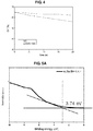
- the quantum yield (QY) of the QD in a layer including only the QDs and a layer including the QDs and the amorphous oxide semiconductor material (a-IGZO) is measured under a temperature condition of 80 °C and is shown in FIG. 4 .
- Indium chloride (0.1M), gallium nitrate hydrate (0.1M), zinc chloride (0.1M) and ethanolamine were dissolved in 2-methoxyethanol and were stirred under a temperature of 50 °C for 1 hr. After the mixture was additionally stirred for 24 hrs, the QDs (10 vol%) in hexane were added. Under N 2 condition, the mixture was coated on the wafer, and the layer was thermally treated under a temperature of 80 °C for 1 hr.
- the proportion of the quantum yield decrease of the QD in the layer including the QDs and the amorphous oxide semiconductor material is decreased. Namely, the oxygen is absorbed by the amorphous oxide semiconductor material such that the damage of the QD is prevented.
- the indium atom, the gallium atom and the zinc atom may have a difference in their mole fractions.
- the gallium atom and the zinc atom respectively have a first mole fraction and a second mole fraction with respect to the indium atom.
- the gallium atom has a third mole fraction, which is greater than the first mole fraction, with respect to the indium atom.
- the zinc atom has a fourth mole fraction, which is greater than the second mole fraction, with respect to the indium atom.
- the mole fraction of each of the gallium atom and the zinc atom with respect to the indium atom may be greater than the first and second mole fraction, respectively.
- the gallium atom and the zinc atom respectively have a fifth mole fraction and a sixth mole fraction.
- the fifth and sixth mole fractions are respectively smaller than the first and second mole fractions.
- the mole ratio of the indium atom, the gallium atom and the zinc atom may be 1:1:1.
- the mole ratio of the indium atom, the gallium atom and the zinc atom may be 1:1.1 ⁇ 3:1.1 ⁇ 3.
- the mole ratio of the indium atom, the gallium atom and the zinc atom may be 1.1 ⁇ 3:1:1.
- the first to third amorphous oxide semiconductor materials 272 to 276 have a difference in a valence band maximum level (or a highest occupied molecular orbital (HOMO) maximum level).
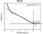
- FIGs. 5A to 5E are graphs showing UPS (ultraviolet photoelectron spectroscopy) measuring results of the amorphous oxide semiconductor materials having different mole fractions of the indium atom, the gallium atom and the zinc atom, and the valence band maximum level (VBM) of the amorphous oxide semiconductor material according to the mole fraction of the indium atom, the gallium atom and the zinc atom is listed in Table 1.
- UPS ultraviolet photoelectron spectroscopy
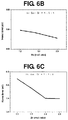
- FIGs. 6A to 6C are graphs showing changes of a valence band maximum level of an amorphous oxide semiconductor material according to a mole fraction of indium, gallium and zinc.
- Table 1 Mole fraction VBM In Ga Zn IGZO (Ex1) 1 1 1 8.24 eV IGZO (Ex2) 2 1 1 8.48 eV IGZO 1.7 1 1 8.33 eV IGZO 2.4 1 1 8.50 eV IGZO (Ex3) 3 1 1 8.57 eV IGZO (Ex4) 1 1 2 7.51 eV IGZO 1 1 1.5 7.89 eV IGZO 1 1 2.5 7.47 eV IGZO (Ex5) 1 2 1 8.14 eV IGZO 1 2 2 8.02 eV
- FIGs. 5A to 5E and FIGs. 6A to 6C with respect to the amorphous oxide semiconductor material having the indium/gallium/zinc mole ratio of 1:1:1, the valence band maximum level of the amorphous oxide semiconductor material is increased when the indium mole fraction is increased, and the valence band maximum level of the amorphous oxide semiconductor material is decreased when the gallium mole fraction and/or the zinc mole fraction is increased.
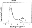
- FIGs. 7A and 7B The UPS results of the green QD having InP/ZnSe/ZnS structure are shown in FIGs. 7A and 7B
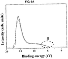
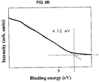
- the UPS results of the red QD having InP/ZnSe/ZnS structure are shown in FIGs. 8A and 8B
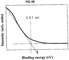
- the UPS results of the blue QD having ZnSe/ZnS structure are shown in FIGs. 9A and 9B .
- FIGs. 7B , 8B and 8B are enlarged view of the "A", “B" and "C" portions in FIGs. 7A , 8A and 9A , respectively.
- the valence band maximum level of the above QDs is listed in Table 2.
- Table 2 QD VBM Green 8.42 eV Red 8.25 eV Blue 8.59 eV
- the valence band maximum level of the green QD is greater than that of the red QD and smaller than that of the blue QD.
- the valence band maximum level of the first QD 262 in the green pixel GP is greater than that of the second QD 264 in the red pixel RP and smaller than that of the third QD 266 in the blue pixel BP.
- the first amorphous oxide semiconductor material 272 in the green pixel GP has the valence band maximum level being greater than the second amorphous oxide semiconductor material 274 in the red pixel RP and being smaller than the third amorphous oxide semiconductor material 276 in the blue pixel BP.
- the first QD 262 in the first pixel P1 and the second QD 264 in the second pixel P2 have a difference in the valence band maximum level
- the first amorphous oxide semiconductor material 272 in the first pixel P1 and the second amorphous oxide semiconductor material 274 in the second pixel P2 also have a difference in the valence band maximum level.
- the mole fractions of the indium atom, the gallium atom and the zinc atom are different.
- the indium atom, the gallium atom and the zinc atom have different mole fractions.
- the mole fraction of the gallium atom with respect to the indium atom in the second amorphous oxide semiconductor material 274 is greater than that in the first amorphous oxide semiconductor material 272.
- the mole fraction of the zinc atom with respect to the indium atom in the second amorphous oxide semiconductor material 274 is greater than that in the first amorphous oxide semiconductor material 272.
- the third QD 266 in the third pixel P3 has a different valence band maximum level from the first and second QDs 262 and 264 respectively in the first and second pixels P1 and P2, and the third amorphous oxide semiconductor material 276 in the third pixel P3 has a different valence band maximum level from the first and second amorphous oxide semiconductor materials 272 and 274 respectively in the first and second pixels P1 and P2.
- the mole fraction of the indium atom, the gallium atom and the zinc atom is different.
- the indium atom and the third amorphous oxide semiconductor material 276 in the third pixel P3, the indium atom, the gallium atom and the zinc atom have different mole fractions.
- the mole fraction of the indium atom with respect to the gallium atom and/or the zinc atom in the third amorphous oxide semiconductor material 276 is greater than that in the first and second amorphous oxide semiconductor materials 272 and 274.
- the charge injection transfer property into the QDs 262 to 266 is improved.
- the emitting property of the emitting diode D and the electroluminescent display device 100 is improved.
- the emitting diode is fabricated by sequentially stacking the anode, the HIL, the ETL, the EML, the ETL and the cathode.
- the property of the emitting diode with changing the mole fraction of the indium atom, the gallium atom and the zinc atom in the amorphous oxide semiconductor material of the EML in the green, red and blue pixels is measured and listed in Table 3.
- the emitting property of the emitting diode D is further improved.
- the QDs 262 to 266 and the amorphous oxide semiconductor materials 272 to 276 are included in the EML 230 of the emitting layer 170, the damages on the QDs 262 to 266 by the external moisture and/or oxygen are prevented.
- the QDs 262 to 266 are dispersed in the amorphous oxide semiconductor materials 272 to 276, the aggregation of the QDs 262 to 266 is prevented such that the emitting efficiency decrease by QD quenching is prevented.
- the charge transfer property is improved such that the emitting property of the emitting diode D and the electroluminescent display device 100 is further improved.
- the valence band maximum level of the amorphous oxide semiconductor material is matched to that of the QD, the emitting property of the emitting diode D and the electroluminescent display device 100 is further improved.
- FIG. 10 is a schematic cross-sectional view of an electroluminescent display device according to a second embodiment of the present invention.
- the electroluminescent display device 300 includes a first or lower substrate 310, a TFT Tr on or over the first substrate 310, an emitting diode D connected to the TFT Tr and a color conversion layer 350 on or over the emitting diode D.
- the first substrate 310 may be a glass substrate or a plastic substrate.
- the first substrate 310 may be formed of polyimide.
- the TFT Tr may include a semiconductor layer, a gate electrode, a source electrode and a drain electrode.
- a passivation layer 320 which includes a contact hole 322, is formed to cover the TFT Tr.
- the drain electrode of the TFT Tr may be exposed by the contact hole 322.
- the emitting diode D is formed on the passivation layer 320 and connected to the TFT Tr through the contact hole 322.
- the emitting diode D may be a white emitting diode.
- the emitting diode D includes a first electrode 330, a second electrode 334 facing the first electrode 330 and an emitting layer 332 between the first and second electrodes 330 and 334, and the white light is emitted from the emitting layer 332.
- the emitting layer 332 may be formed by one-body to cover all of a red pixel RP, a green pixel GP and a blue pixel BP.
- the first electrode 330 may be an anode and may be formed of a conductive material having a relatively high work function.
- the first electrode 330 may be formed of a transparent conductive material such as indium-tin-oxide (ITO) or indium-zinc-oxide (IZO).
- a reflection electrode or a reflection layer may be formed under the first electrode 330.
- the reflection electrode or the reflection layer may be formed of aluminum-palladium-copper (APC) alloy.
- the second electrode 334 may be formed of a conductive material having a relatively low work function to serve as a cathode.
- the second electrode 34 may be formed of aluminum (Al), magnesium (Mg) or Al-Mg alloy.
- the second electrode 334 When the electroluminescent display device 300 is operated in a top-emission type, the second electrode 334 has a thin thickness to transmit the light.
- the emitting layer 332 which is positioned between the first and second electrodes 330 and 334, may include a first emitting part ST1, which includes a first EML 476, a second emitting part ST2, which includes a second EML 484, and a charge generation layer 490 between the first and second emitting parts ST1 and ST2.
- the first emitting part ST1, the charge generation layer 490 and the second emitting part ST2 are sequentially stacked on the first electrode 330. Namely, the first emitting part ST1 is positioned between the first electrode 330 and the charge generation layer 490, and the second emitting part ST2 is positioned between the second electrode 334 and the charge generation layer 490.
- the first emitting part ST1 may further include an HIL 472 between the first electrode 330 and the first EML 476, a first HTL 474 between the HIL 472 and the first EML 476 and a first ETL 478 between the first EML 476 and the charge generation layer 490. At least one of the HIL 472, the first HTL 474 and the first ETL 478 may be omitted.
- the second emitting part ST2 may further include a second HTL 482 between the charge generation layer 490 and the second EML 484, a second ETL 486 between the second EML 484 and the second electrode 334 and an EIL 488 between the second ETL 486 and the second electrode 334. At least one of the second HTL 482, the second ETL 486 and the EIL 488 may be omitted.
- the charge generation layer 490 is positioned between the first and second parts ST1 and ST2. Namely, the first and second emitting parts ST1 and ST2 are connected by the charge generation layer 490.
- the charge generation layer 490 may be a PN junction layer of an N-type charge generation layer 490N and a P-type charge generation layer 490P.
- the N-type charge generation layer 490N is positioned between the first ETL 478 and the second HTL 482, and the P-type charge generation layer 490P is positioned between the N-type charge generation layer 490N and the second HTL 482.
- the charge generation layer 490 generates charges or separates the charge into the hole and the electron such that the hole and the electron are respectively provided into the second emitting part ST2 and the first emitting part ST1.
- the N-type charge generation layer 490N provides the electron into the first ETL 478 of the first emitting part ST1, and the first ETL 478 provides the electron into the first EML 476 adjacent to the first electrode 330.
- the P-type charge generation layer 490P provides the hole into the second HTL 482 of the second emitting part ST2, and the second HTL 482 provides the hole into the second EML 484 adjacent to the second electrode 334. Accordingly, the emitting efficiency of the emitting diode D including the first and second EMLs 476 and 484 is improved, and the driving voltage of the emitting diode D is lowered.
- one of the first and second EMLs 476 and 484 may include a blue emitting material, and the other one of the first and second EMLs 476 and 484 may include a yellow emitting material.
- the lights emitted from the first and second EMLs 476 and 484 are mixed such that the white light is emitted from the emitting diode D.
- each of the blue emitting material and the yellow emitting material may be an organic emitting material having a phosphorescent property or a fluorescent property or an inorganic emitting material such as the QD.
- a second or upper substrate 340 is disposed over the emitting diode D, and the color conversion layer 350 is formed on an inner side of the second substrate 340.
- the color conversion layer 350 includes first to third color conversion layers 352, 354 and 356 respectively corresponding to the green, red and blue pixels GP, RP and BP.
- the first color conversion layer 352 includes a first QD 362 and a first amorphous oxide semiconductor material 372, and a second color conversion layer 354 includes a second QD 364 and a second amorphous oxide semiconductor material 374.
- a third color conversion layer 356 includes a third QD 366 and a third amorphous oxide semiconductor material 376.
- the first to third QDs 362 to 366 are green, red and blue QDs, respectively, such that the electroluminescent display device 300 can provide a color image.
- the first to third amorphous oxide semiconductor materials 372 to 376 may be a-IGZO.
- the first to third amorphous oxide semiconductor materials 372 to 376 serve as a protection layer (or a base layer) blocking or preventing the penetration of external moisture to the QDs 362 to 366.
- the penetration of oxygen to the QDs 362 to 366 is also blocked or prevented by the first to third amorphous oxide semiconductor materials 372 to 376.
- first to third QDs 362 to 366 are dispersed in the first to third amorphous oxide semiconductor materials 372 to 376 such that the aggregation of the QDs 362 to 366 is prevented. As a result, the emitting efficiency decrease by QD quenching is prevented.
- the amorphous oxide semiconductor materials 372 to 376 can be cured by a relatively low curing process of about 100 to 150 °C, the damage on the QDs 362 to 366 by a high curing process is prevented.
- the energy level of the amorphous oxide semiconductor materials 372 to 376 is matched to that of the QDs 362 to 366, the extinction efficiency of the QDs 362 to 366 to the light energy from the emitting diode D, i.e., the light energy absorbing efficiency, and the emitting property of the QDs 362 to 366 are improved.
- the indium atom, the gallium atom and the zinc atom may have the same mole fraction.
- the indium atom, the gallium atom and the zinc atom may have a difference in their mole fractions.
- the first to third amorphous oxide semiconductor materials 372 to 376 may also have a difference in the valence band maximum level.
- the valence band maximum level of the first QD 362 in the green pixel GP is greater than that of the second QD 364 in the red pixel RP and smaller than that of the third QD 366 in the blue pixel BP.
- the first QD 362 of the first color conversion layer 352 in the first pixel P1 and the second QD 364 of the second color conversion layer 354 in the second pixel P2 have a difference in the valence band maximum level
- the first amorphous oxide semiconductor material 372 of the first color conversion layer 352 in the first pixel P1 and the second amorphous oxide semiconductor material 374 of the second color conversion layer 354 in the second pixel P2 also have a difference in the valence band maximum level.
- the mole fractions of the indium atom, the gallium atom and the zinc atom are different.
- the indium atom, the gallium atom and the zinc atom have different mole fractions.
- the mole fraction of the gallium atom with respect to the indium atom in the second amorphous oxide semiconductor material 374 is greater than that in the first amorphous oxide semiconductor material 372.
- the mole fraction of the zinc atom with respect to the indium atom in the second amorphous oxide semiconductor material 374 is greater than that in the first amorphous oxide semiconductor material 372.
- the third QD 366 of the third color conversion layer 356 in the third pixel P3 has a different valence band maximum level from the first and second QDs 362 and 364 of the first and second color conversion layers 352 and 354 in the first and second pixels P1 and P2, respectively, and the third amorphous oxide semiconductor material 376 of the third color conversion layer 356 in the third pixel P3 has a different valence band maximum level from the first and second amorphous oxide semiconductor materials 372 and 374 of the first and second color conversion layers 352 and 354 in the first and second pixels P1 and P2, respectively.
- the mole fraction of the indium atom, the gallium atom and the zinc atom is different.
- the second amorphous oxide semiconductor material 374 in the second color conversion layer 354 the indium atom and the third amorphous oxide semiconductor material 376 in the third color conversion layer 356, the indium atom, the gallium atom and the zinc atom have different mole fractions.
- the mole fraction of the indium atom with respect to the gallium atom and/or the zinc atom in the third amorphous oxide semiconductor material 376 is greater than that in the first and second amorphous oxide semiconductor materials 372 and 374.
- the color conversion layer 350 is spaced apart from the second electrode 334, but it is not limited thereto.
- the color conversion layer 350 may contact the second electrode 334 or may be adhered onto the second electrode 334 by an adhesive layer.
- the color conversion layer 350 may be positioned between the emitting diode D and the first substrate 310 in a bottom-emission type electroluminescent display device.
- a green color filter, a red color filter and a blue color filter may be positioned between each of the first to third color conversion layers 352, 354 and 356 and the second substrate 340.
Landscapes
- Physics & Mathematics (AREA)
- Optics & Photonics (AREA)
- Engineering & Computer Science (AREA)
- Chemical & Material Sciences (AREA)
- Crystallography & Structural Chemistry (AREA)
- Inorganic Chemistry (AREA)
- Nanotechnology (AREA)
- Geometry (AREA)
- Microelectronics & Electronic Packaging (AREA)
- Electroluminescent Light Sources (AREA)
- Devices For Indicating Variable Information By Combining Individual Elements (AREA)
Abstract
Description
- The present application claims the benefit of Korean Patent Application No.
10-2017-0140214 - The present disclosure relates to a display device, and more particularly, to an emitting diode and an electroluminescent display device each having improved lifespan and emitting property.
- As information technology and mobile communication technology have been developed, a display device being capable of displaying a visual image has also been developed. Flat panel display devices, such as a liquid crystal display (LCD) device a plasma display panel (PDP) device and an electroluminescent display device, are developed and used because of advantages in weight, power consumption, and so on.
- The electroluminescent display device includes an emitting diode, and the emitting diode includes an electron injection electrode (i.e., cathode), a hole injection electrode (i.e., anode) and an emitting layer therebetween. The electron from the cathode and the hole from the anode are injected into the emitting layer to form an exciton, and the exciton is transited from the excited state to the ground state such that the light is emitted from the emitting diode.
- The electroluminescent display device may include a red pixel, a green pixel and a blue pixel, and red light, green light and blue light are respectively emitted from the emitting diode in the red, green and blue pixels such that a color image is provided.
- Recently, use of a quantum dot (QD) to display devices has been researched or studied.
- In the QD, an electron in an unstable state transitions from a conduction band to a valence band such that light is emitted. Since the QD has a high extinction coefficient and excellent quantum yield (QY), strong fluorescent light is emitted from the QD. In addition, since the wavelength of the light from the QD is controlled by a size of the QD, entire visible light can be emitted by controlling the size of the QD.
-
FIG. 1 is a schematic cross-sectional view of the related art emitting diode using a QD. - As shown in
FIG. 1 , the emitting diode D includes afirst electrode 10 as an anode, asecond electrode 20 as a cathode and facing thefirst electrode 10 and anemitting layer 30 positioned between the first andsecond electrodes QDs 40, an electron transporting layer (ETL) 37 and an electron injection layer (EIL) 39. - In the emitting diode D, the hole is transferred from the
first electrode 10 into theEML 35 through theHIL 31 and theHTL 33, and the electron is transferred from thesecond electrode 20 into theEML 35 through the EIL 39 and theETL 37. As a result, the light is emitted from theQD 40 in the EML 35. - However, there are problem of short lifespan and low emitting efficiency in the related art emitting diode D. Namely, the emitting diode is exposed to moisture such that the lifespan and the emitting efficiency of the emitting diode D are lowered.
- Accordingly, the present invention is directed to an emitting diode and an electroluminescent display device that substantially obviate one or more of the problems due to limitations and disadvantages of the related art.
- An object of the present invention is to provide an emitting diode and an electroluminescent display device having improved lifespan and emitting efficiency.
- Additional features and advantages of the invention will be set forth in the description which follows, and in part will be apparent from the description, or may be learned by practice of the invention. The objectives and other advantages of the invention will be realized and attained by the structure particularly pointed out in the written description and claims hereof as well as the appended drawings.
- To achieve these and other advantages and in accordance with the purpose of the present invention, as embodied and broadly described herein, an emitting diode comprises a first electrode in a first (e.g. green) pixel; a first emitting layer positioned on the first electrode and in the first pixel and including a first amorphous oxide semiconductor material and a first quantum dot, wherein the first amorphous oxide semiconductor material includes an indium atom, a gallium atom and a zinc atom; and a second electrode covering the first emitting layer.
- The emitting diode may further comprise a second emitting layer in a second (e.g. red) pixel and including a second amorphous oxide semiconductor material and a second quantum dot, wherein the second amorphous oxide semiconductor material includes an indium atom, a gallium atom and a zinc atom.
- In the emitting diode, a mole fraction of the indium atom, the gallium atom or the zinc atom in the first amorphous oxide semiconductor material may differ from a corresponding mole fraction in the second amorphous oxide semiconductor material.
- In the first amorphous oxide semiconductor material the gallium atom may have a first mole fraction with respect to the indium atom, and in the second amorphous oxide semiconductor material, the gallium atom may have a second mole fraction with respect to the indium atom, wherein the second mole fraction is greater than the first mole fraction.
- In the first amorphous oxide semiconductor material, the zinc atom may have a third mole fraction with respect to the indium atom, and in the second amorphous oxide semiconductor material, the zinc atom may have a fourth mole fraction with respect to the indium atom, wherein the fourth mole fraction is greater than the third mole fraction.
- The first quantum dot may have a valence band maximum level greater than that of the second quantum dot, and the first amorphous oxide semiconductor material may have a valence band maximum level greater than that of the second amorphous oxide semiconductor material.
- The emitting diode may further comprise a third emitting layer in a third (e.g. blue) pixel and include a third amorphous oxide semiconductor material and a third quantum dot, wherein the third amorphous oxide semiconductor material includes an indium atom, a gallium atom and a zinc atom.
- In the emitting diode, a mole fraction of the indium atom, the gallium atom or the zinc atom in the first amorphous oxide semiconductor material may differ from a corresponding mole fraction in the third amorphous oxide semiconductor material.
- In the first amorphous oxide semiconductor material, the indium atom may have a fifth mole fraction with respect to the gallium atom, and in the third amorphous oxide semiconductor material, the indium atom may have a sixth mole fraction with respect to the gallium atom, wherein the sixth mole fraction is greater than the fifth mole fraction.
- The first quantum dot may have a valence band maximum level smaller than that of the third quantum dot, and the first amorphous oxide semiconductor material may have a valence band maximum level smaller than that of the third amorphous oxide semiconductor material.
- In another aspect, an electroluminescent display device comprises any one of the aforementioned emitting diodes on a substrate, and a thin film transistor is positioned between the substrate and the emitting diode and is connected to the first electrode.
- In another aspect, an electroluminescent display device comprises a lower substrate including a first (e.g. green) pixel; an emitting diode on the lower substrate; a thin film transistor positioned between the lower substrate and the emitting diode and connected to the emitting diode; and a first color conversion layer in the first pixel, wherein the first color conversion layer includes a first amorphous oxide semiconductor material and a first quantum dot, and the first amorphous oxide semiconductor material includes an indium atom, a gallium atom and a zinc atom.
- In the electroluminescent display device, the first color conversion layer may be positioned between the lower substrate and the emitting diode or between the emitting diode and an upper substrate.
- The electroluminescent display device may further comprise a second color conversion layer disposed in a second (e.g. red) pixel and may include a second amorphous oxide semiconductor material and a second quantum dot, wherein the second amorphous oxide semiconductor material may include an indium atom, a gallium atom and a zinc atom.
- A mole fraction of the indium atom, the gallium atom or the zinc atom in the first amorphous oxide semiconductor material may differ from a corresponding mole fraction in the second amorphous oxide semiconductor material.
- In the first amorphous oxide semiconductor material, the gallium atom may have a first mole fraction with respect to the indium atom, and in the second amorphous oxide semiconductor material, the gallium atom may have a second mole fraction with respect to the indium atom, wherein the second mole fraction is greater than the first mole fraction.
- In the first amorphous oxide semiconductor material, the zinc atom has a third mole fraction with respect to the indium atom, and in the second amorphous oxide semiconductor material, the zinc atom has a fourth mole fraction with respect to the indium atom, wherein the fourth mole fraction is greater than the third mole fraction.
- In the electroluminescent display device, the first quantum dot may have a valence band maximum level greater than that of the second quantum dot, and the first amorphous oxide semiconductor material may have a valence band maximum level greater than that of the second amorphous oxide semiconductor material.
- The electroluminescent display device may further comprise a third emitting layer in a third (e.g. blue) pixel and may include a third amorphous oxide semiconductor material and a third quantum dot, wherein the third amorphous oxide semiconductor material may include an indium atom, a gallium atom and a zinc atom.
- A mole fraction of the indium atom, the gallium atom or the zinc atom in the first amorphous oxide semiconductor material may differ from a corresponding mole fraction of the indium atom, the gallium atom and the zinc atom in the third amorphous oxide semiconductor material.
- In the first amorphous oxide semiconductor material, the indium atom may have a fifth mole fraction with respect to the gallium atom, and in the third amorphous oxide semiconductor material, the indium atom may have a sixth mole fraction with respect to the gallium atom, wherein the sixth mole fraction is greater than the fifth mole fraction.
- In the electroluminescent display device, the first quantum dot may have a valence band maximum level smaller than that of the third quantum dot, and the first amorphous oxide semiconductor material may have a valence band maximum level smaller than that of the third amorphous oxide semiconductor material.
- It is to be understood that both the foregoing general description and the following detailed description are exemplary and explanatory and are intended to provide further explanation of the invention as claimed.
- The accompanying drawings, which are included to provide a further understanding of the invention and are incorporated in and constitute a part of this specification, illustrate embodiments of the invention and together with the description serve to explain the principles of the invention.
-
FIG. 1 is a schematic cross-sectional view of the related art emitting diode using a QD. -
FIG. 2 is a schematic cross-sectional view of an electroluminescent display device according to a first embodiment of the present invention. -
FIGs. 3A to 3C are schematic cross-sectional views of an emitting diode in each pixel of the electroluminescent display device according to the first embodiment of the present invention. -
FIG. 4 is a graph illustrating an emitting efficiency of a QD layer with an amorphous oxide semiconductor material. -
FIGs. 5A to 5E are graphs showing UPS (ultraviolet photoelectron spectroscopy) measuring results of amorphous oxide semiconductor materials. -
FIGs. 6A to 6C are graphs showing changes of a valence band maximum level of an amorphous oxide semiconductor material according to a mole fraction of indium, gallium and zinc, respectively. -
FIGs. 7A and7B are graphs showing UPS measuring results of a green QD. -
FIGs. 8A and8B are graphs showing UPS measuring results of a red QD. -
FIGs. 9A and9B are graphs showing UPS measuring results of a blue QD. -
FIG. 10 is a schematic cross-sectional view of an electroluminescent display device according to a second embodiment of the present invention. -
FIG. 11 is a schematic cross-sectional view of an emitting diode of the electroluminescent display device according toFigure 10 . - Reference will now be made in detail to the preferred embodiments, examples of which are illustrated in the accompanying drawings.
-
FIG. 2 is a schematic cross-sectional view of an electroluminescent display device according to a first embodiment of the present invention. - As shown in
FIG. 2 , theelectroluminescent display device 100 according to the first embodiment of the present invention includes asubstrate 110, a thin film transistor (TFT) Tr on or over thesubstrate 110 and an emitting diode D connected to the TFT Tr. - The
substrate 110 may be a glass substrate or a plastic substrate. For example, thesubstrate 110 may be formed of polyimide. - A
buffer layer 120 is formed on thesubstrate 110, and the TFT Tr is formed on thebuffer layer 110. Thebuffer layer 120 may be omitted. - A semiconductor layer 122 is formed on the
buffer layer 120. The semiconductor layer 122 may include an oxide semiconductor material or polycrystalline silicon. - When the semiconductor layer 122 includes the oxide semiconductor material, a light-shielding pattern (not shown) may be formed under the semiconductor layer 122. The light to the semiconductor layer 122 is shielded or blocked by the light-shielding pattern such that thermal degradation of the semiconductor layer 122 can be prevented. On the other hand, when the semiconductor layer 122 includes polycrystalline silicon, impurities may be doped into both sides of the semiconductor layer 122.
- A
gate insulating layer 124 is formed on the semiconductor layer 122. Thegate insulating layer 124 may be formed of an inorganic insulating material such as silicon oxide or silicon nitride. - A
gate electrode 130, which is formed of a conductive material, e.g., metal, is formed on thegate insulating layer 124 to correspond to a center of the semiconductor layer 122. - In
FIG. 2 , thegate insulating layer 124 is formed on an entire surface of thesubstrate 110. Alternatively, thegate insulating layer 124 may be patterned to have the same shape as thegate electrode 130. - An interlayer insulating
layer 132, which is formed of an insulating material, is formed on thegate electrode 130. The interlayer insulatinglayer 132 may be formed of an inorganic insulating material, e.g., silicon oxide or silicon nitride, or an organic insulating material, e.g., benzocyclobutene or photo-acryl. - The interlayer insulating
layer 132 includes first and second contact holes 134 and 136 exposing both sides of the semiconductor layer 122. The first and second contact holes 134 and 136 are positioned at both sides of thegate electrode 130 to be spaced apart from thegate electrode 130. - The first and second contact holes 134 and 136 are formed through the
gate insulating layer 124. Alternatively, when thegate insulating layer 124 is patterned to have the same shape as thegate electrode 130, the first and second contact holes 134 and 136 is formed only through the interlayer insulatinglayer 132. - A
source electrode 140 and adrain electrode 142, which are formed of a conductive material, e.g., metal, are formed on theinterlayer insulating layer 132. - The
source electrode 140 and thedrain electrode 142 are spaced apart from each other with respect to thegate electrode 130 and respectively contact both sides of the semiconductor layer 122 through the first and second contact holes 134 and 136. - The semiconductor layer 122, the
gate electrode 130, thesource electrode 140 and thedrain electrode 142 constitute the TFT as a driving element. - The
gate electrode 130, thesource electrode 140, and thedrain electrode 142 are positioned over the semiconductor layer 122. Namely, the TFT Tr has a coplanar structure. - Alternatively, in the TFT Tr, the gate electrode may be positioned under the semiconductor layer, and the source and drain electrodes may be positioned over the semiconductor layer such that the TFT Tr may have an inverted staggered structure. In this instance, the semiconductor layer may include amorphous silicon.
- Although not shown, a gate line and a data line are disposed on or over the
substrate 110 and cross each other to define a pixel region. In addition, a switching element, which is electrically connected to the gate line and the data line, may be disposed on thesubstrate 110. The switching element is electrically connected to the TFT Tr as the driving element. - In addition, a power line, which is parallel to and spaced apart from the gate line or the data line, may be formed on or over the
substrate 110. Moreover, a storage capacitor for maintaining a voltage of thegate electrode 130 of the TFT Tr during one frame, may be further formed on thesubstrate 110. - A
passivation layer 150, which includes adrain contact hole 152 exposing thedrain electrode 142 of the TFT Tr, is formed to cover the TFT Tr. - A
first electrode 160, which is connected to thedrain electrode 142 of the TFT Tr through thedrain contact hole 152, is separately formed in each pixel region. Thefirst electrode 160 may be an anode and may be formed of a conductive material having a relatively high work function. For example, thefirst electrode 160 may be formed of a transparent conductive material such as indium-tin-oxide (ITO) or indium-zinc-oxide (IZO). - When the
electroluminescent display device 100 is operated in a top-emission type, a reflection electrode or a reflection layer may be formed under thefirst electrode 160. For example, the reflection electrode or the reflection layer may be formed of aluminum-palladium-copper (APC) alloy. - A
bank 166 is formed on thepassivation layer 150 to cover an edge of thefirst electrode 160. Thebank 166 exposes a center of thefirst electrode 160 in correspondence to the pixel region. - An emitting
layer 170 is formed on thefirst electrode 160. The emittinglayer 170 includes a QD and an amorphous oxide semiconductor material. - The QD may include a core and a shell surrounding (covering) the core. Each of the core and the shell may be formed of a semiconductor compound. Each of the core and the shell may be formed of a II-VI group compound or a III-V group compound in the periodic table.
- For example, the core may be formed of one of CdSe, CdS, CdTe, ZnO, ZnSe, ZnS, ZnTe, HgSe, HgTe, CdZnSe, InP, InN, GaN, InSb, InAsP, InGaAs, GaAs, GaP, GaSb, AlP, AlN, AlAs, AlSb, CdSeTe and ZnCdSe, and the shell may be formed of the other one of CdSe, CdS, CdTe, ZnO, ZnSe, ZnS, ZnTe, HgSe, HgTe, CdZnSe, InP, InN, GaN, InSb, InAsP, InGaAs, GaAs, GaP, GaSb, AlP, AlN, AlAs, AlSb, CdSeTe and ZnCdSe.
- The amorphous oxide semiconductor material may be amorphous indium-gallium-zinc oxide (a-IGZO).
- The emitting
layer 170 may have a single-layered structure of the EML including the QD and the amorphous oxide semiconductor material. To improve an emitting efficiency of the emitting diode D, the emittinglayer 170 may have a multi-layered structure of the HIL, the HTL, the EML, the ETL and the EIL. - A
second electrode 180 is formed over thesubstrate 110 including the emittinglayer 170. Thesecond electrode 180 covers an entire surface of a display region and may be formed of a conductive material having a relatively low work function to serve as a cathode. For example, thesecond electrode 180 may be formed of aluminum (Al), magnesium (Mg) or Al-Mg alloy. - The
first electrode 160, the emittinglayer 170 and thesecond electrode 180 constitute the emitting diode D. - An
encapsulation film 190 is formed on thesecond electrode 180 to block or prevent the penetration of external moisture into the emitting diode D. For example, theencapsulation film 190 may include a first inorganic insulating layer 192, an organic insulatinglayer 194 and a second inorganic insulatinglayer 196 sequentially stacked, but it is not limited thereto. - In addition, a polarization plate (not shown) may be attached on an outer side of the
encapsulation film 190 to reduce an ambient light reflection. For example, the polarization plate may be a circular polarization plate. -
FIGs. 3A to 3C are schematic cross-sectional views of an emitting diode in each pixel of the electroluminescent display device according to the first embodiment of the present invention. - As shown in
FIGs. 3A to 3C , the emitting diode D in each of a green pixel GP, a red pixel RP and a blue pixel BP includes thefirst electrode 160, thesecond electrode 180 facing thefirst electrode 160 and the emittinglayer 170 positioned between the first andsecond electrodes EML 230. Afirst EML 232 in the green pixel GP includes afirst QD 262 and a first amorphousoxide semiconductor material 272. Asecond EML 234 in the red pixel RP includes asecond QD 264 and a second amorphousoxide semiconductor material 274. Athird EML 236 in the blue pixel BP includes athird QD 266 and a third amorphousoxide semiconductor material 276. - In addition, the emitting
layer 170 may further include theHTL 220 between thefirst electrode 160 and theEML 230 and theHIL 210 between thefirst electrode 160 and theHTL 220. Further, the emittinglayer 170 may further include theETL 240 between theEML 230 and thesecond electrode 180 and theEIL 250 between theETL 240 and thesecond electrode 180. At least one of theHTL 220, theHIL 210, theETL 240 and theEIL 250 may be omitted. - The first to
third QD - The first to third amorphous
oxide semiconductor materials oxide semiconductor materials 272 to 276, the indium atom, the gallium atom and the zinc atom may have the same mole fraction. - The first to third amorphous
oxide semiconductor materials 272 to 276 serve as a protection layer (or a base layer) blocking or preventing the penetration of external moisture to theQDs 262 to 266. In addition, due to the gallium atom having strong combination strength with oxygen, the penetration of oxygen to theQDs 262 to 266 is also blocked or prevented by the first to third amorphousoxide semiconductor materials 272 to 276. - Moreover, since an energy level of the first to third amorphous
oxide semiconductor materials 272 to 276 is matched with the energy level of the first tothird QDs 262 to 266, the charge transfer property is improved such that the emitting property of the emitting diode D is improved. - Furthermore, the first to
third QDs 262 to 266 are dispersed in the first to third amorphousoxide semiconductor materials 272 to 276 such that the aggregation of theQDs 262 to 266 is prevented. As a result, the emitting efficiency decrease by QD quenching is prevented. - On the other hand, when a crystalline oxide semiconductor material is used instead of the amorphous oxide semiconductor material, the
QDs 262 to 266 may be damaged. Namely, since a high temperature curing process of about 300 to 350 °C is required to cure the crystalline oxide semiconductor material, the damage on theQDs 262 to 266 may be generated by the high temperature curing process. However, since the amorphous oxide semiconductor material can be cured by a low temperature curing process of about 100 to 150 °C, the above damage on theQDs 262 to 266 can be prevented. - The quantum yield (QY) of the QD in a layer including only the QDs and a layer including the QDs and the amorphous oxide semiconductor material (a-IGZO) is measured under a temperature condition of 80 °C and is shown in
FIG. 4 . - (1) Formation of the layer including the QDs and the amorphous oxide semiconductor material (a-IGZO)
- Indium chloride (0.1M), gallium nitrate hydrate (0.1M), zinc chloride (0.1M) and ethanolamine were dissolved in 2-methoxyethanol and were stirred under a temperature of 50 °C for 1 hr. After the mixture was additionally stirred for 24 hrs, the QDs (10 vol%) in hexane were added. Under N2 condition, the mixture was coated on the wafer, and the layer was thermally treated under a temperature of 80 °C for 1 hr.
- As shown in
FIG. 4 , the proportion of the quantum yield decrease of the QD in the layer including the QDs and the amorphous oxide semiconductor material (a-IGZO) is decreased. Namely, the oxygen is absorbed by the amorphous oxide semiconductor material such that the damage of the QD is prevented. - Alternatively, in the first to third amorphous
oxide semiconductor materials 272 to 276, the indium atom, the gallium atom and the zinc atom may have a difference in their mole fractions. - Namely, in the first amorphous
oxide semiconductor material 272, the gallium atom and the zinc atom respectively have a first mole fraction and a second mole fraction with respect to the indium atom. In the second amorphousoxide semiconductor material 274, the gallium atom has a third mole fraction, which is greater than the first mole fraction, with respect to the indium atom. In the second amorphousoxide semiconductor material 274, the zinc atom has a fourth mole fraction, which is greater than the second mole fraction, with respect to the indium atom. In addition, in the second amorphousoxide semiconductor material 274, the mole fraction of each of the gallium atom and the zinc atom with respect to the indium atom may be greater than the first and second mole fraction, respectively. - In the third amorphous
oxide semiconductor material 276, the gallium atom and the zinc atom respectively have a fifth mole fraction and a sixth mole fraction. The fifth and sixth mole fractions are respectively smaller than the first and second mole fractions. - For example, in the first amorphous
oxide semiconductor material 272, the mole ratio of the indium atom, the gallium atom and the zinc atom may be 1:1:1. In the second amorphousoxide semiconductor material 274, the mole ratio of the indium atom, the gallium atom and the zinc atom may be 1:1.1∼3:1.1∼3. In the third amorphousoxide semiconductor material 276, the mole ratio of the indium atom, the gallium atom and the zinc atom may be 1.1∼3:1:1. - Since the indium atom, the gallium atom and the zinc atom have different mole fractions in the first to third amorphous
oxide semiconductor materials 272 to 276, the first to third amorphousoxide semiconductor materials 272 to 276 have a difference in a valence band maximum level (or a highest occupied molecular orbital (HOMO) maximum level). -
FIGs. 5A to 5E are graphs showing UPS (ultraviolet photoelectron spectroscopy) measuring results of the amorphous oxide semiconductor materials having different mole fractions of the indium atom, the gallium atom and the zinc atom, and the valence band maximum level (VBM) of the amorphous oxide semiconductor material according to the mole fraction of the indium atom, the gallium atom and the zinc atom is listed in Table 1. - In addition,
FIGs. 6A to 6C are graphs showing changes of a valence band maximum level of an amorphous oxide semiconductor material according to a mole fraction of indium, gallium and zinc.Table 1 Mole fraction VBM In Ga Zn IGZO (Ex1) 1 1 1 8.24 eV IGZO (Ex2) 2 1 1 8.48 eV IGZO 1.7 1 1 8.33 eV IGZO 2.4 1 1 8.50 eV IGZO (Ex3) 3 1 1 8.57 eV IGZO (Ex4) 1 1 2 7.51 eV IGZO 1 1 1.5 7.89 eV IGZO 1 1 2.5 7.47 eV IGZO (Ex5) 1 2 1 8.14 eV IGZO 1 2 2 8.02 eV - As shown in Table 1,
FIGs. 5A to 5E andFIGs. 6A to 6C , with respect to the amorphous oxide semiconductor material having the indium/gallium/zinc mole ratio of 1:1:1, the valence band maximum level of the amorphous oxide semiconductor material is increased when the indium mole fraction is increased, and the valence band maximum level of the amorphous oxide semiconductor material is decreased when the gallium mole fraction and/or the zinc mole fraction is increased. - The UPS results of the green QD having InP/ZnSe/ZnS structure are shown in
FIGs. 7A and7B , the UPS results of the red QD having InP/ZnSe/ZnS structure are shown inFIGs. 8A and8B , and the UPS results of the blue QD having ZnSe/ZnS structure are shown inFIGs. 9A and9B .FIGs. 7B ,8B and 8B are enlarged view of the "A", "B" and "C" portions inFIGs. 7A ,8A and9A , respectively. The valence band maximum level of the above QDs is listed in Table 2.Table 2 QD VBM Green 8.42 eV Red 8.25 eV Blue 8.59 eV - As shown in Table 2, the valence band maximum level of the green QD is greater than that of the red QD and smaller than that of the blue QD.
- Accordingly, in the emitting diode D of the present invention, the valence band maximum level of the
first QD 262 in the green pixel GP is greater than that of thesecond QD 264 in the red pixel RP and smaller than that of thethird QD 266 in the blue pixel BP. To match the energy level of the first to third amorphousoxide semiconductor materials 272 to 276 with the first tothird QDs 262 to 266, the first amorphousoxide semiconductor material 272 in the green pixel GP has the valence band maximum level being greater than the second amorphousoxide semiconductor material 274 in the red pixel RP and being smaller than the third amorphousoxide semiconductor material 276 in the blue pixel BP. - Namely, the
first QD 262 in the first pixel P1 and thesecond QD 264 in the second pixel P2 have a difference in the valence band maximum level, and the first amorphousoxide semiconductor material 272 in the first pixel P1 and the second amorphousoxide semiconductor material 274 in the second pixel P2 also have a difference in the valence band maximum level. In other words, in the first amorphousoxide semiconductor material 272 in the first pixel P1 and the second amorphousoxide semiconductor material 274 in the second pixel P2, the mole fractions of the indium atom, the gallium atom and the zinc atom are different. In the first amorphousoxide semiconductor material 272 in the first pixel P1 and the second amorphousoxide semiconductor material 274 in the second pixel P2, the indium atom, the gallium atom and the zinc atom have different mole fractions. - The mole fraction of the gallium atom with respect to the indium atom in the second amorphous
oxide semiconductor material 274 is greater than that in the first amorphousoxide semiconductor material 272. The mole fraction of the zinc atom with respect to the indium atom in the second amorphousoxide semiconductor material 274 is greater than that in the first amorphousoxide semiconductor material 272. - The
third QD 266 in the third pixel P3 has a different valence band maximum level from the first andsecond QDs oxide semiconductor material 276 in the third pixel P3 has a different valence band maximum level from the first and second amorphousoxide semiconductor materials - In other words, in the first amorphous
oxide semiconductor material 272 in the first pixel P1, the second amorphousoxide semiconductor material 274 in the second pixel P2 and the third amorphousoxide semiconductor material 276 in the third pixel P3, the mole fraction of the indium atom, the gallium atom and the zinc atom is different. In the first amorphousoxide semiconductor material 272 in the first pixel P1, the second amorphousoxide semiconductor material 274 in the second pixel P2, the indium atom and the third amorphousoxide semiconductor material 276 in the third pixel P3, the indium atom, the gallium atom and the zinc atom have different mole fractions. - The mole fraction of the indium atom with respect to the gallium atom and/or the zinc atom in the third amorphous
oxide semiconductor material 276 is greater than that in the first and second amorphousoxide semiconductor materials - In the emitting diode D, since an energy level of the
QDs 262 to 266 and the first to third amorphousoxide semiconductor materials 272 to 276 in the pixels P1, P2 and P3 is sufficiently matched, the charge injection transfer property into theQDs 262 to 266 is improved. - Accordingly, the emitting property of the emitting diode D and the
electroluminescent display device 100 is improved. - The emitting diode is fabricated by sequentially stacking the anode, the HIL, the ETL, the EML, the ETL and the cathode. The property of the emitting diode with changing the mole fraction of the indium atom, the gallium atom and the zinc atom in the amorphous oxide semiconductor material of the EML in the green, red and blue pixels is measured and listed in Table 3.
Table 3 EML Volt (V) QY Cd/m2 CIEx CIEy GP QD 4.3 0.92 280 0.376 0.571 a-IGZO (1:1:1)+QD 3.9 1.18 373 0-377 0-578 a-IGZO (1:2:1)+QD 4.0 1.01 369 0.375 0.5 77 RP QD 5.6 2.76 166 0.681 0.313 a-IGZO (1:2:1)+QD 4.8 3.61 253 0-683 0.31 5 a-IGZO (1:1:2)+QD 5.2 3.05 222 0.681 0.0312 BP QD 4.5 0.018 1.43 ' 0.192 0.106 a-IGZO (2:1:1)+QD 3.9 0.136 10.12 0.197 0.088 - As shown in Table 3, in comparison to the emitting diode with the EML including only QD except the amorphous oxide semiconductor material, the emitting property of the emitting diode with the QD and the amorphous oxide semiconductor material is improved.
- In addition, when the valence band maximum level of the amorphous oxide semiconductor material and the QD in the red, green and blue pixels is matched, the emitting property of the emitting diode D is further improved.
- As mentioned above, in the emitting diode D and the
electroluminescent display device 100 according to the first embodiment of the present invention, theQDs 262 to 266 and the amorphousoxide semiconductor materials 272 to 276 are included in theEML 230 of the emittinglayer 170, the damages on theQDs 262 to 266 by the external moisture and/or oxygen are prevented. In addition, since theQDs 262 to 266 are dispersed in the amorphousoxide semiconductor materials 272 to 276, the aggregation of theQDs 262 to 266 is prevented such that the emitting efficiency decrease by QD quenching is prevented. - Moreover, since the energy level of the amorphous oxide semiconductor materials is matched to that of the, the charge transfer property is improved such that the emitting property of the emitting diode D and the
electroluminescent display device 100 is further improved. - Furthermore, the valence band maximum level of the amorphous oxide semiconductor material is matched to that of the QD, the emitting property of the emitting diode D and the
electroluminescent display device 100 is further improved. -
FIG. 10 is a schematic cross-sectional view of an electroluminescent display device according to a second embodiment of the present invention. - As shown in
FIG. 10 , theelectroluminescent display device 300 according to the second embodiment of the present invention includes a first orlower substrate 310, a TFT Tr on or over thefirst substrate 310, an emitting diode D connected to the TFT Tr and acolor conversion layer 350 on or over the emitting diode D. - The
first substrate 310 may be a glass substrate or a plastic substrate. For example, thefirst substrate 310 may be formed of polyimide. - Although not shown, the TFT Tr may include a semiconductor layer, a gate electrode, a source electrode and a drain electrode.
- A
passivation layer 320, which includes acontact hole 322, is formed to cover the TFT Tr. For example, the drain electrode of the TFT Tr may be exposed by thecontact hole 322. - The emitting diode D is formed on the
passivation layer 320 and connected to the TFT Tr through thecontact hole 322. The emitting diode D may be a white emitting diode. - Namely, the emitting diode D includes a
first electrode 330, asecond electrode 334 facing thefirst electrode 330 and an emittinglayer 332 between the first andsecond electrodes layer 332. The emittinglayer 332 may be formed by one-body to cover all of a red pixel RP, a green pixel GP and a blue pixel BP. - The
first electrode 330 may be an anode and may be formed of a conductive material having a relatively high work function. For example, thefirst electrode 330 may be formed of a transparent conductive material such as indium-tin-oxide (ITO) or indium-zinc-oxide (IZO). - When the
electroluminescent display device 300 is operated in a top-emission type, a reflection electrode or a reflection layer may be formed under thefirst electrode 330. For example, the reflection electrode or the reflection layer may be formed of aluminum-palladium-copper (APC) alloy. - The
second electrode 334 may be formed of a conductive material having a relatively low work function to serve as a cathode. For example, the second electrode 34 may be formed of aluminum (Al), magnesium (Mg) or Al-Mg alloy. - When the
electroluminescent display device 300 is operated in a top-emission type, thesecond electrode 334 has a thin thickness to transmit the light. - Referring to
FIG. 11 , which is a schematic cross-sectional view of an emitting diode of the electroluminescent display device according to the second embodiment of the present invention, the emittinglayer 332, which is positioned between the first andsecond electrodes first EML 476, a second emitting part ST2, which includes asecond EML 484, and acharge generation layer 490 between the first and second emitting parts ST1 and ST2. - The first emitting part ST1, the
charge generation layer 490 and the second emitting part ST2 are sequentially stacked on thefirst electrode 330. Namely, the first emitting part ST1 is positioned between thefirst electrode 330 and thecharge generation layer 490, and the second emitting part ST2 is positioned between thesecond electrode 334 and thecharge generation layer 490. - The first emitting part ST1 may further include an
HIL 472 between thefirst electrode 330 and thefirst EML 476, afirst HTL 474 between theHIL 472 and thefirst EML 476 and afirst ETL 478 between thefirst EML 476 and thecharge generation layer 490. At least one of theHIL 472, thefirst HTL 474 and thefirst ETL 478 may be omitted. - The second emitting part ST2 may further include a
second HTL 482 between thecharge generation layer 490 and thesecond EML 484, asecond ETL 486 between thesecond EML 484 and thesecond electrode 334 and anEIL 488 between thesecond ETL 486 and thesecond electrode 334. At least one of thesecond HTL 482, thesecond ETL 486 and theEIL 488 may be omitted. - The
charge generation layer 490 is positioned between the first and second parts ST1 and ST2. Namely, the first and second emitting parts ST1 and ST2 are connected by thecharge generation layer 490. For example, thecharge generation layer 490 may be a PN junction layer of an N-typecharge generation layer 490N and a P-typecharge generation layer 490P. - The N-type
charge generation layer 490N is positioned between thefirst ETL 478 and thesecond HTL 482, and the P-typecharge generation layer 490P is positioned between the N-typecharge generation layer 490N and thesecond HTL 482. - The
charge generation layer 490 generates charges or separates the charge into the hole and the electron such that the hole and the electron are respectively provided into the second emitting part ST2 and the first emitting part ST1. - The N-type
charge generation layer 490N provides the electron into thefirst ETL 478 of the first emitting part ST1, and thefirst ETL 478 provides the electron into thefirst EML 476 adjacent to thefirst electrode 330. The P-typecharge generation layer 490P provides the hole into thesecond HTL 482 of the second emitting part ST2, and thesecond HTL 482 provides the hole into thesecond EML 484 adjacent to thesecond electrode 334. Accordingly, the emitting efficiency of the emitting diode D including the first and second EMLs 476 and 484 is improved, and the driving voltage of the emitting diode D is lowered. - For example, one of the first and second EMLs 476 and 484 may include a blue emitting material, and the other one of the first and second EMLs 476 and 484 may include a yellow emitting material. The lights emitted from the first and second EMLs 476 and 484 are mixed such that the white light is emitted from the emitting diode D.
- For example, each of the blue emitting material and the yellow emitting material may be an organic emitting material having a phosphorescent property or a fluorescent property or an inorganic emitting material such as the QD.
- A second or
upper substrate 340 is disposed over the emitting diode D, and thecolor conversion layer 350 is formed on an inner side of thesecond substrate 340. - The
color conversion layer 350 includes first to third color conversion layers 352, 354 and 356 respectively corresponding to the green, red and blue pixels GP, RP and BP. - The first
color conversion layer 352 includes afirst QD 362 and a first amorphousoxide semiconductor material 372, and a secondcolor conversion layer 354 includes asecond QD 364 and a second amorphousoxide semiconductor material 374. A thirdcolor conversion layer 356 includes athird QD 366 and a third amorphousoxide semiconductor material 376. - The first to
third QDs 362 to 366 are green, red and blue QDs, respectively, such that theelectroluminescent display device 300 can provide a color image. - The first to third amorphous
oxide semiconductor materials 372 to 376 may be a-IGZO. - The first to third amorphous
oxide semiconductor materials 372 to 376 serve as a protection layer (or a base layer) blocking or preventing the penetration of external moisture to theQDs 362 to 366. In addition, due to the gallium atom having strong combination strength with oxygen, the penetration of oxygen to theQDs 362 to 366 is also blocked or prevented by the first to third amorphousoxide semiconductor materials 372 to 376. - Moreover, the first to
third QDs 362 to 366 are dispersed in the first to third amorphousoxide semiconductor materials 372 to 376 such that the aggregation of theQDs 362 to 366 is prevented. As a result, the emitting efficiency decrease by QD quenching is prevented. - Furthermore, since the amorphous
oxide semiconductor materials 372 to 376 can be cured by a relatively low curing process of about 100 to 150 °C, the damage on theQDs 362 to 366 by a high curing process is prevented. - Since the energy level of the amorphous
oxide semiconductor materials 372 to 376 is matched to that of theQDs 362 to 366, the extinction efficiency of theQDs 362 to 366 to the light energy from the emitting diode D, i.e., the light energy absorbing efficiency, and the emitting property of theQDs 362 to 366 are improved. - In the first to third amorphous
oxide semiconductor materials 372 to 376, the indium atom, the gallium atom and the zinc atom may have the same mole fraction. Alternatively, in the first to third amorphousoxide semiconductor materials 372 to 376, the indium atom, the gallium atom and the zinc atom may have a difference in their mole fractions. - As mentioned above, since the
QDs 362 to 366 have a difference in the valence band maximum level, the first to third amorphousoxide semiconductor materials 372 to 376 may also have a difference in the valence band maximum level. - For example, the valence band maximum level of the
first QD 362 in the green pixel GP is greater than that of thesecond QD 364 in the red pixel RP and smaller than that of thethird QD 366 in the blue pixel BP. - Namely, the
first QD 362 of the firstcolor conversion layer 352 in the first pixel P1 and thesecond QD 364 of the secondcolor conversion layer 354 in the second pixel P2 have a difference in the valence band maximum level, and the first amorphousoxide semiconductor material 372 of the firstcolor conversion layer 352 in the first pixel P1 and the second amorphousoxide semiconductor material 374 of the secondcolor conversion layer 354 in the second pixel P2 also have a difference in the valence band maximum level. In other words, in the first amorphousoxide semiconductor material 372 of the firstcolor conversion layer 352 and in the second amorphousoxide semiconductor material 374 of the secondcolor conversion layer 354, the mole fractions of the indium atom, the gallium atom and the zinc atom are different. In the first amorphousoxide semiconductor material 372 of the firstcolor conversion layer 352 and the second amorphousoxide semiconductor material 374 of the secondcolor conversion layer 354, the indium atom, the gallium atom and the zinc atom have different mole fractions. - The mole fraction of the gallium atom with respect to the indium atom in the second amorphous
oxide semiconductor material 374 is greater than that in the first amorphousoxide semiconductor material 372. The mole fraction of the zinc atom with respect to the indium atom in the second amorphousoxide semiconductor material 374 is greater than that in the first amorphousoxide semiconductor material 372. - The
third QD 366 of the thirdcolor conversion layer 356 in the third pixel P3 has a different valence band maximum level from the first andsecond QDs oxide semiconductor material 376 of the thirdcolor conversion layer 356 in the third pixel P3 has a different valence band maximum level from the first and second amorphousoxide semiconductor materials - In other words, in the first amorphous
oxide semiconductor material 372 in the firstcolor conversion layer 352, the second amorphousoxide semiconductor material 374 in the secondcolor conversion layer 354 and the third amorphousoxide semiconductor material 376 in the thirdcolor conversion layer 356, the mole fraction of the indium atom, the gallium atom and the zinc atom is different. In the first amorphousoxide semiconductor material 372 in the firstcolor conversion layer 352, the second amorphousoxide semiconductor material 374 in the secondcolor conversion layer 354, the indium atom and the third amorphousoxide semiconductor material 376 in the thirdcolor conversion layer 356, the indium atom, the gallium atom and the zinc atom have different mole fractions. - The mole fraction of the indium atom with respect to the gallium atom and/or the zinc atom in the third amorphous
oxide semiconductor material 376 is greater than that in the first and second amorphousoxide semiconductor materials - In
FIG. 10 , thecolor conversion layer 350 is spaced apart from thesecond electrode 334, but it is not limited thereto. For example, thecolor conversion layer 350 may contact thesecond electrode 334 or may be adhered onto thesecond electrode 334 by an adhesive layer. In another example, thecolor conversion layer 350 may be positioned between the emitting diode D and thefirst substrate 310 in a bottom-emission type electroluminescent display device. - Although not shown, a green color filter, a red color filter and a blue color filter may be positioned between each of the first to third color conversion layers 352, 354 and 356 and the
second substrate 340. - It will be apparent to those skilled in the art that various modifications and variations can be made in the present invention within the scope of the appended claims.
Claims (15)
- An emitting diode (D), comprising:a first electrode (160) in a first pixel (GP);a first emitting layer (170) positioned on the first electrode (160) and in the first pixel (GP) and including a first amorphous oxide semiconductor material (272) and a first quantum dot (262), wherein the first amorphous oxide semiconductor material (272) includes an indium atom, a gallium atom and a zinc atom; anda second electrode (180) covering the first emitting layer (170).
- The emitting diode (D) according to claim 1, further comprising: a second emitting layer (170) in a second pixel (RP) and including a second amorphous oxide semiconductor material (274) and a second quantum dot (264), wherein the second amorphous oxide semiconductor material (274) includes an indium atom, a gallium atom and a zinc atom.
- The emitting diode (D) according to claim 2, wherein a mole fraction of the indium atom, the gallium atom or the zinc atom in the first amorphous oxide semiconductor material (272) differs from a corresponding mole fraction in the second amorphous oxide semiconductor material (274).
- The emitting diode (D) according to claim 3, wherein, in the first amorphous oxide semiconductor material (272), the gallium atom has a first mole fraction with respect to the indium atom, and in the second amorphous oxide semiconductor material (274), the gallium atom has a second mole fraction with respect to the indium atom,
wherein the second mole fraction is greater than the first mole fraction. - The emitting diode (D) according to claim 3 or 4, wherein, in the first amorphous oxide semiconductor material (272), the zinc atom has a third mole fraction with respect to the indium atom, and in the second amorphous oxide semiconductor material (274), the zinc atom has a fourth mole fraction with respect to the indium atom,
wherein the fourth mole fraction is greater than the third mole fraction. - The emitting diode (D) according to any one of claims 1 to 5, wherein the first quantum dot (262) has a valence band maximum level greater than that of the second quantum dot (264), and the first amorphous oxide semiconductor material (272) has a valence band maximum level greater than that of the second amorphous oxide semiconductor material (274).
- The emitting diode (D) according to any one of claims 1 to 6, further comprising: a third emitting layer (170) in a third pixel (BP) and including a third amorphous oxide semiconductor material (276) and a third quantum dot (266), wherein the third amorphous oxide semiconductor material (276) includes an indium atom, a gallium atom and a zinc atom.
- The emitting diode (D) according to claim 7, wherein a mole fraction of the indium atom, the gallium atom or the zinc atom in the first amorphous oxide semiconductor material (272) differs from a corresponding mole fraction in the third amorphous oxide semiconductor material (276).
- The emitting diode (D) according to claim 7 or 8, wherein, in the first amorphous oxide semiconductor material (272), the indium atom has a fifth mole fraction with respect to the gallium atom, and in the third amorphous oxide semiconductor material (276), the indium atom has a sixth mole fraction with respect to the gallium atom,
wherein the sixth mole fraction is greater than the fifth mole fraction. - The emitting diode (D) according to any one of claims 7 to 9, wherein the first quantum dot (262) has a valence band maximum level smaller than that of the third quantum dot (266), and the first amorphous oxide semiconductor material (272) has a valence band maximum level smaller than that of the third amorphous oxide semiconductor material (276).
- An electroluminescent display device, comprising an emitting diode (D) according to any one of claims 1 to 10, wherein:the emitting diode (D) is disposed on a substrate (110); anda thin film transistor (Tr) is positioned between the substrate (110) and the emitting diode (D) and is connected (136) to the first electrode (160).
- An electroluminescent display device, comprising:a lower substrate (310) including a first pixel (GP);an emitting diode (D, 330, 332, 334) on the lower substrate (310);a thin film transistor (Tr) positioned between the lower substrate (310) and the emitting diode (D) and connected (322) to the emitting diode (D); anda first color conversion layer (352) in the first pixel (GP),wherein the first color conversion layer (352) includes a first amorphous oxide semiconductor material (372) and a first quantum dot (362), and the first amorphous oxide semiconductor material (372) includes an indium atom, a gallium atom and a zinc atom.
- The electroluminescent display device according to claim 12, wherein the first color conversion layer (352) is positioned between the lower substrate (310) and the emitting diode (D) or between the emitting diode (D) and an upper substrate (340).
- The electroluminescent display device according to claim 12 or 13, further comprising: a second color conversion layer (354) disposed in a second pixel (RP) and including a second amorphous oxide semiconductor material (374) and a second quantum dot (364), wherein the second amorphous oxide semiconductor material includes an indium atom, a gallium atom and a zinc atom.
- The electroluminescent display device according to claim 14, wherein a mole fraction of the indium atom, the gallium atom or the zinc atom in the first amorphous oxide semiconductor material (372) differs from a corresponding mole fraction in the second amorphous oxide semiconductor material (374).
Applications Claiming Priority (1)
| Application Number | Priority Date | Filing Date | Title |
|---|---|---|---|
| KR1020170140214A KR102355917B1 (en) | 2017-10-26 | 2017-10-26 | Light emitting diode and Electroluminescent display device |
Publications (2)
| Publication Number | Publication Date |
|---|---|
| EP3477712A1 true EP3477712A1 (en) | 2019-05-01 |
| EP3477712B1 EP3477712B1 (en) | 2019-11-13 |
Family
ID=64017302
Family Applications (1)
| Application Number | Title | Priority Date | Filing Date |
|---|---|---|---|
| EP18202300.2A Active EP3477712B1 (en) | 2017-10-26 | 2018-10-24 | Light emitting diode and electroluminescent display device |
Country Status (4)
| Country | Link |
|---|---|
| US (1) | US10770623B2 (en) |
| EP (1) | EP3477712B1 (en) |
| KR (1) | KR102355917B1 (en) |
| CN (1) | CN109713144B (en) |
Families Citing this family (4)
| Publication number | Priority date | Publication date | Assignee | Title |
|---|---|---|---|---|
| US12040429B2 (en) * | 2018-12-10 | 2024-07-16 | Sharp Kabushiki Kaisha | Light-emitting element and light-emitting device |
| KR20210142031A (en) * | 2020-05-14 | 2021-11-24 | 삼성디스플레이 주식회사 | Display apparatus |
| KR102798046B1 (en) * | 2020-11-11 | 2025-04-22 | 삼성디스플레이 주식회사 | Display apparatus |
| JP7768717B2 (en) * | 2021-10-05 | 2025-11-12 | シャープ福山レーザー株式会社 | Micro light emitting element and image display element |
Citations (3)
| Publication number | Priority date | Publication date | Assignee | Title |
|---|---|---|---|---|
| US20120138894A1 (en) * | 2009-07-07 | 2012-06-07 | University Of Florida Research Foundation Inc. | Stable and all solution processable quantum dot light-emitting diodes |
| US20150194467A1 (en) * | 2013-06-26 | 2015-07-09 | Boe Technology Group Co., Ltd | Double-sided display apparatus and method of manufacturing the same |
| US20150228850A1 (en) * | 2012-09-26 | 2015-08-13 | Univerity Of Florida Research Foundaton, Inc. | Transparent quantum dot light-emitting diodes with dielectric/metal/dielectric electrode |
Family Cites Families (6)
| Publication number | Priority date | Publication date | Assignee | Title |
|---|---|---|---|---|
| DE102011112000B4 (en) * | 2011-08-31 | 2023-11-30 | OSRAM Opto Semiconductors Gesellschaft mit beschränkter Haftung | LED chip |
| CN103579380A (en) | 2012-08-09 | 2014-02-12 | 索尼公司 | Light-receiving or light-emitting component, solar cell, optical sensor and LED |
| KR102332836B1 (en) | 2013-03-26 | 2021-12-01 | 가부시키가이샤 한도오따이 에네루기 켄큐쇼 | Light-emitting element, compound, organic compound, display module, lighting module, light-emitting device, display device, lighting device, and electronic device |
| KR102335452B1 (en) * | 2015-06-16 | 2021-12-07 | 서울바이오시스 주식회사 | Light emitting device |
| KR102609932B1 (en) * | 2015-09-09 | 2023-12-04 | 이노럭스 코포레이션 | Display device |
| CN105810848B (en) | 2016-03-16 | 2017-12-19 | 京东方科技集团股份有限公司 | A kind of preparation method of quantum dot layer and QLED display devices, preparation method containing quantum dot layer |
-
2017
- 2017-10-26 KR KR1020170140214A patent/KR102355917B1/en active Active
-
2018
- 2018-10-24 EP EP18202300.2A patent/EP3477712B1/en active Active
- 2018-10-24 US US16/169,191 patent/US10770623B2/en active Active
- 2018-10-25 CN CN201811252297.5A patent/CN109713144B/en active Active
Patent Citations (3)
| Publication number | Priority date | Publication date | Assignee | Title |
|---|---|---|---|---|
| US20120138894A1 (en) * | 2009-07-07 | 2012-06-07 | University Of Florida Research Foundation Inc. | Stable and all solution processable quantum dot light-emitting diodes |
| US20150228850A1 (en) * | 2012-09-26 | 2015-08-13 | Univerity Of Florida Research Foundaton, Inc. | Transparent quantum dot light-emitting diodes with dielectric/metal/dielectric electrode |
| US20150194467A1 (en) * | 2013-06-26 | 2015-07-09 | Boe Technology Group Co., Ltd | Double-sided display apparatus and method of manufacturing the same |
Also Published As
| Publication number | Publication date |
|---|---|
| US10770623B2 (en) | 2020-09-08 |
| KR20190046423A (en) | 2019-05-07 |
| KR102355917B1 (en) | 2022-01-25 |
| CN109713144A (en) | 2019-05-03 |
| CN109713144B (en) | 2020-12-15 |
| EP3477712B1 (en) | 2019-11-13 |
| US20190131492A1 (en) | 2019-05-02 |
Similar Documents
| Publication | Publication Date | Title |
|---|---|---|
| US11489092B2 (en) | Quantum-dot film, LED package, quantum-dot light emitting diode and display device | |
| US11849594B2 (en) | Quantum dot emitting diode and quantum dot display device including the same | |
| US9768404B1 (en) | Quantum dot spacing for high efficiency quantum dot LED displays | |
| US11251389B2 (en) | Quantum dot, quantum dot light emitting diode and quantum dot display device | |
| US10700236B2 (en) | Quantum dot spacing for high efficiency quantum dot LED displays | |
| US11744094B2 (en) | Quantum-dot light emitting diode, method of fabricating the quantum-dot light emitting diode and quantum-dot light emitting display device | |
| EP3477712B1 (en) | Light emitting diode and electroluminescent display device | |
| EP3316325B1 (en) | Quantum dot light emitting diode and quantum dot display device including the same | |
| US10790411B2 (en) | Quantum dot LED with spacer particles | |
| US20140117335A1 (en) | Organic light emitting diode display | |
| KR20210080923A (en) | Quantum dot solution composition, Quantum dot film and Quantum dot display device | |
| KR20180031845A (en) | Inorganic emitting particle, Inorganic emitting particle film, and LED package and Display device including the same | |
| US11127913B2 (en) | Quantum-dot light emitting diode and quantum-dot light emitting display device | |
| KR102595367B1 (en) | White organic light emitting device | |
| US11832466B2 (en) | Electroluminescent element and display device | |
| US11489130B2 (en) | Quantum-dot light emitting diode and quantum-dot light emitting display device including the same | |
| US20220165973A1 (en) | Light emitting element and display device using same |
Legal Events
| Date | Code | Title | Description |
|---|---|---|---|
| PUAI | Public reference made under article 153(3) epc to a published international application that has entered the european phase |
Free format text: ORIGINAL CODE: 0009012 |
|
| STAA | Information on the status of an ep patent application or granted ep patent |
Free format text: STATUS: REQUEST FOR EXAMINATION WAS MADE |
|
| 17P | Request for examination filed |
Effective date: 20181024 |
|
| AK | Designated contracting states |
Kind code of ref document: A1 Designated state(s): AL AT BE BG CH CY CZ DE DK EE ES FI FR GB GR HR HU IE IS IT LI LT LU LV MC MK MT NL NO PL PT RO RS SE SI SK SM TR |
|
| AX | Request for extension of the european patent |
Extension state: BA ME |
|
| GRAP | Despatch of communication of intention to grant a patent |
Free format text: ORIGINAL CODE: EPIDOSNIGR1 |
|
| STAA | Information on the status of an ep patent application or granted ep patent |
Free format text: STATUS: GRANT OF PATENT IS INTENDED |
|
| INTG | Intention to grant announced |
Effective date: 20190527 |
|
| GRAS | Grant fee paid |
Free format text: ORIGINAL CODE: EPIDOSNIGR3 |
|
| GRAA | (expected) grant |
Free format text: ORIGINAL CODE: 0009210 |
|
| STAA | Information on the status of an ep patent application or granted ep patent |
Free format text: STATUS: THE PATENT HAS BEEN GRANTED |
|
| AK | Designated contracting states |
Kind code of ref document: B1 Designated state(s): AL AT BE BG CH CY CZ DE DK EE ES FI FR GB GR HR HU IE IS IT LI LT LU LV MC MK MT NL NO PL PT RO RS SE SI SK SM TR |
|
| REG | Reference to a national code |
Ref country code: AT Ref legal event code: REF Ref document number: 1202580 Country of ref document: AT Kind code of ref document: T Effective date: 20191115 Ref country code: CH Ref legal event code: EP |
|
| REG | Reference to a national code |
Ref country code: DE Ref legal event code: R096 Ref document number: 602018001183 Country of ref document: DE |
|
| REG | Reference to a national code |
Ref country code: IE Ref legal event code: FG4D |
|
| REG | Reference to a national code |
Ref country code: NL Ref legal event code: FP |
|
| REG | Reference to a national code |
Ref country code: LT Ref legal event code: MG4D |
|
| PG25 | Lapsed in a contracting state [announced via postgrant information from national office to epo] |
Ref country code: FI Free format text: LAPSE BECAUSE OF FAILURE TO SUBMIT A TRANSLATION OF THE DESCRIPTION OR TO PAY THE FEE WITHIN THE PRESCRIBED TIME-LIMIT Effective date: 20191113 Ref country code: BG Free format text: LAPSE BECAUSE OF FAILURE TO SUBMIT A TRANSLATION OF THE DESCRIPTION OR TO PAY THE FEE WITHIN THE PRESCRIBED TIME-LIMIT Effective date: 20200213 Ref country code: LT Free format text: LAPSE BECAUSE OF FAILURE TO SUBMIT A TRANSLATION OF THE DESCRIPTION OR TO PAY THE FEE WITHIN THE PRESCRIBED TIME-LIMIT Effective date: 20191113 Ref country code: LV Free format text: LAPSE BECAUSE OF FAILURE TO SUBMIT A TRANSLATION OF THE DESCRIPTION OR TO PAY THE FEE WITHIN THE PRESCRIBED TIME-LIMIT Effective date: 20191113 Ref country code: SE Free format text: LAPSE BECAUSE OF FAILURE TO SUBMIT A TRANSLATION OF THE DESCRIPTION OR TO PAY THE FEE WITHIN THE PRESCRIBED TIME-LIMIT Effective date: 20191113 Ref country code: PL Free format text: LAPSE BECAUSE OF FAILURE TO SUBMIT A TRANSLATION OF THE DESCRIPTION OR TO PAY THE FEE WITHIN THE PRESCRIBED TIME-LIMIT Effective date: 20191113 Ref country code: GR Free format text: LAPSE BECAUSE OF FAILURE TO SUBMIT A TRANSLATION OF THE DESCRIPTION OR TO PAY THE FEE WITHIN THE PRESCRIBED TIME-LIMIT Effective date: 20200214 Ref country code: NO Free format text: LAPSE BECAUSE OF FAILURE TO SUBMIT A TRANSLATION OF THE DESCRIPTION OR TO PAY THE FEE WITHIN THE PRESCRIBED TIME-LIMIT Effective date: 20200213 Ref country code: PT Free format text: LAPSE BECAUSE OF FAILURE TO SUBMIT A TRANSLATION OF THE DESCRIPTION OR TO PAY THE FEE WITHIN THE PRESCRIBED TIME-LIMIT Effective date: 20200313 |
|
| PG25 | Lapsed in a contracting state [announced via postgrant information from national office to epo] |
Ref country code: IS Free format text: LAPSE BECAUSE OF FAILURE TO SUBMIT A TRANSLATION OF THE DESCRIPTION OR TO PAY THE FEE WITHIN THE PRESCRIBED TIME-LIMIT Effective date: 20200313 Ref country code: RS Free format text: LAPSE BECAUSE OF FAILURE TO SUBMIT A TRANSLATION OF THE DESCRIPTION OR TO PAY THE FEE WITHIN THE PRESCRIBED TIME-LIMIT Effective date: 20191113 Ref country code: HR Free format text: LAPSE BECAUSE OF FAILURE TO SUBMIT A TRANSLATION OF THE DESCRIPTION OR TO PAY THE FEE WITHIN THE PRESCRIBED TIME-LIMIT Effective date: 20191113 |
|
| PG25 | Lapsed in a contracting state [announced via postgrant information from national office to epo] |
Ref country code: AL Free format text: LAPSE BECAUSE OF FAILURE TO SUBMIT A TRANSLATION OF THE DESCRIPTION OR TO PAY THE FEE WITHIN THE PRESCRIBED TIME-LIMIT Effective date: 20191113 |
|
| PG25 | Lapsed in a contracting state [announced via postgrant information from national office to epo] |
Ref country code: ES Free format text: LAPSE BECAUSE OF FAILURE TO SUBMIT A TRANSLATION OF THE DESCRIPTION OR TO PAY THE FEE WITHIN THE PRESCRIBED TIME-LIMIT Effective date: 20191113 Ref country code: RO Free format text: LAPSE BECAUSE OF FAILURE TO SUBMIT A TRANSLATION OF THE DESCRIPTION OR TO PAY THE FEE WITHIN THE PRESCRIBED TIME-LIMIT Effective date: 20191113 Ref country code: CZ Free format text: LAPSE BECAUSE OF FAILURE TO SUBMIT A TRANSLATION OF THE DESCRIPTION OR TO PAY THE FEE WITHIN THE PRESCRIBED TIME-LIMIT Effective date: 20191113 Ref country code: DK Free format text: LAPSE BECAUSE OF FAILURE TO SUBMIT A TRANSLATION OF THE DESCRIPTION OR TO PAY THE FEE WITHIN THE PRESCRIBED TIME-LIMIT Effective date: 20191113 Ref country code: EE Free format text: LAPSE BECAUSE OF FAILURE TO SUBMIT A TRANSLATION OF THE DESCRIPTION OR TO PAY THE FEE WITHIN THE PRESCRIBED TIME-LIMIT Effective date: 20191113 |
|
| REG | Reference to a national code |
Ref country code: DE Ref legal event code: R097 Ref document number: 602018001183 Country of ref document: DE |
|
| REG | Reference to a national code |
Ref country code: AT Ref legal event code: MK05 Ref document number: 1202580 Country of ref document: AT Kind code of ref document: T Effective date: 20191113 |
|
| PG25 | Lapsed in a contracting state [announced via postgrant information from national office to epo] |
Ref country code: SK Free format text: LAPSE BECAUSE OF FAILURE TO SUBMIT A TRANSLATION OF THE DESCRIPTION OR TO PAY THE FEE WITHIN THE PRESCRIBED TIME-LIMIT Effective date: 20191113 Ref country code: SM Free format text: LAPSE BECAUSE OF FAILURE TO SUBMIT A TRANSLATION OF THE DESCRIPTION OR TO PAY THE FEE WITHIN THE PRESCRIBED TIME-LIMIT Effective date: 20191113 |
|
| PLBE | No opposition filed within time limit |
Free format text: ORIGINAL CODE: 0009261 |
|
| STAA | Information on the status of an ep patent application or granted ep patent |
Free format text: STATUS: NO OPPOSITION FILED WITHIN TIME LIMIT |
|
| 26N | No opposition filed |
Effective date: 20200814 |
|
| PG25 | Lapsed in a contracting state [announced via postgrant information from national office to epo] |
Ref country code: AT Free format text: LAPSE BECAUSE OF FAILURE TO SUBMIT A TRANSLATION OF THE DESCRIPTION OR TO PAY THE FEE WITHIN THE PRESCRIBED TIME-LIMIT Effective date: 20191113 |
|
| PG25 | Lapsed in a contracting state [announced via postgrant information from national office to epo] |
Ref country code: IT Free format text: LAPSE BECAUSE OF FAILURE TO SUBMIT A TRANSLATION OF THE DESCRIPTION OR TO PAY THE FEE WITHIN THE PRESCRIBED TIME-LIMIT Effective date: 20191113 |
|
| PG25 | Lapsed in a contracting state [announced via postgrant information from national office to epo] |
Ref country code: SI Free format text: LAPSE BECAUSE OF FAILURE TO SUBMIT A TRANSLATION OF THE DESCRIPTION OR TO PAY THE FEE WITHIN THE PRESCRIBED TIME-LIMIT Effective date: 20191113 |
|
| PG25 | Lapsed in a contracting state [announced via postgrant information from national office to epo] |
Ref country code: LU Free format text: LAPSE BECAUSE OF NON-PAYMENT OF DUE FEES Effective date: 20201024 Ref country code: MC Free format text: LAPSE BECAUSE OF FAILURE TO SUBMIT A TRANSLATION OF THE DESCRIPTION OR TO PAY THE FEE WITHIN THE PRESCRIBED TIME-LIMIT Effective date: 20191113 |
|
| REG | Reference to a national code |
Ref country code: BE Ref legal event code: MM Effective date: 20201031 |
|
| PG25 | Lapsed in a contracting state [announced via postgrant information from national office to epo] |
Ref country code: BE Free format text: LAPSE BECAUSE OF NON-PAYMENT OF DUE FEES Effective date: 20201031 |
|
| PG25 | Lapsed in a contracting state [announced via postgrant information from national office to epo] |
Ref country code: IE Free format text: LAPSE BECAUSE OF NON-PAYMENT OF DUE FEES Effective date: 20201024 |
|
| REG | Reference to a national code |
Ref country code: CH Ref legal event code: PL |
|
| PG25 | Lapsed in a contracting state [announced via postgrant information from national office to epo] |
Ref country code: TR Free format text: LAPSE BECAUSE OF FAILURE TO SUBMIT A TRANSLATION OF THE DESCRIPTION OR TO PAY THE FEE WITHIN THE PRESCRIBED TIME-LIMIT Effective date: 20191113 Ref country code: MT Free format text: LAPSE BECAUSE OF FAILURE TO SUBMIT A TRANSLATION OF THE DESCRIPTION OR TO PAY THE FEE WITHIN THE PRESCRIBED TIME-LIMIT Effective date: 20191113 Ref country code: CY Free format text: LAPSE BECAUSE OF FAILURE TO SUBMIT A TRANSLATION OF THE DESCRIPTION OR TO PAY THE FEE WITHIN THE PRESCRIBED TIME-LIMIT Effective date: 20191113 |
|
| PG25 | Lapsed in a contracting state [announced via postgrant information from national office to epo] |
Ref country code: MK Free format text: LAPSE BECAUSE OF FAILURE TO SUBMIT A TRANSLATION OF THE DESCRIPTION OR TO PAY THE FEE WITHIN THE PRESCRIBED TIME-LIMIT Effective date: 20191113 |
|
| PG25 | Lapsed in a contracting state [announced via postgrant information from national office to epo] |
Ref country code: LI Free format text: LAPSE BECAUSE OF NON-PAYMENT OF DUE FEES Effective date: 20211031 Ref country code: CH Free format text: LAPSE BECAUSE OF NON-PAYMENT OF DUE FEES Effective date: 20211031 |
|
| REG | Reference to a national code |
Ref country code: DE Ref legal event code: R079 Ref document number: 602018001183 Country of ref document: DE Free format text: PREVIOUS MAIN CLASS: H01L0033060000 Ipc: H10H0020812000 |
|
| PGFP | Annual fee paid to national office [announced via postgrant information from national office to epo] |
Ref country code: NL Payment date: 20250821 Year of fee payment: 8 |
|
| PGFP | Annual fee paid to national office [announced via postgrant information from national office to epo] |
Ref country code: GB Payment date: 20250820 Year of fee payment: 8 |
|
| PGFP | Annual fee paid to national office [announced via postgrant information from national office to epo] |
Ref country code: FR Payment date: 20250821 Year of fee payment: 8 |
|
| PGFP | Annual fee paid to national office [announced via postgrant information from national office to epo] |
Ref country code: DE Payment date: 20250820 Year of fee payment: 8 |