EP3477694A1 - Power semiconductor module with partially coated power terminals - Google Patents
Power semiconductor module with partially coated power terminals Download PDFInfo
- Publication number
- EP3477694A1 EP3477694A1 EP18202737.5A EP18202737A EP3477694A1 EP 3477694 A1 EP3477694 A1 EP 3477694A1 EP 18202737 A EP18202737 A EP 18202737A EP 3477694 A1 EP3477694 A1 EP 3477694A1
- Authority
- EP
- European Patent Office
- Prior art keywords
- power
- plastic housing
- power terminals
- contact
- substrate
- Prior art date
- Legal status (The legal status is an assumption and is not a legal conclusion. Google has not performed a legal analysis and makes no representation as to the accuracy of the status listed.)
- Granted
Links
Images



Classifications
-
- H—ELECTRICITY
- H10—SEMICONDUCTOR DEVICES; ELECTRIC SOLID-STATE DEVICES NOT OTHERWISE PROVIDED FOR
- H10W—GENERIC PACKAGES, INTERCONNECTIONS, CONNECTORS OR OTHER CONSTRUCTIONAL DETAILS OF DEVICES COVERED BY CLASS H10
- H10W72/00—Interconnections or connectors in packages
-
- H—ELECTRICITY
- H10—SEMICONDUCTOR DEVICES; ELECTRIC SOLID-STATE DEVICES NOT OTHERWISE PROVIDED FOR
- H10W—GENERIC PACKAGES, INTERCONNECTIONS, CONNECTORS OR OTHER CONSTRUCTIONAL DETAILS OF DEVICES COVERED BY CLASS H10
- H10W76/00—Containers; Fillings or auxiliary members therefor; Seals
- H10W76/01—Manufacture or treatment
-
- H—ELECTRICITY
- H10—SEMICONDUCTOR DEVICES; ELECTRIC SOLID-STATE DEVICES NOT OTHERWISE PROVIDED FOR
- H10W—GENERIC PACKAGES, INTERCONNECTIONS, CONNECTORS OR OTHER CONSTRUCTIONAL DETAILS OF DEVICES COVERED BY CLASS H10
- H10W76/00—Containers; Fillings or auxiliary members therefor; Seals
- H10W76/10—Containers or parts thereof
- H10W76/12—Containers or parts thereof characterised by their shape
- H10W76/15—Containers comprising an insulating or insulated base
-
- H—ELECTRICITY
- H10—SEMICONDUCTOR DEVICES; ELECTRIC SOLID-STATE DEVICES NOT OTHERWISE PROVIDED FOR
- H10W—GENERIC PACKAGES, INTERCONNECTIONS, CONNECTORS OR OTHER CONSTRUCTIONAL DETAILS OF DEVICES COVERED BY CLASS H10
- H10W76/00—Containers; Fillings or auxiliary members therefor; Seals
- H10W76/10—Containers or parts thereof
- H10W76/12—Containers or parts thereof characterised by their shape
- H10W76/15—Containers comprising an insulating or insulated base
- H10W76/153—Containers comprising an insulating or insulated base having interconnections in passages through the insulating or insulated base
-
- H—ELECTRICITY
- H10—SEMICONDUCTOR DEVICES; ELECTRIC SOLID-STATE DEVICES NOT OTHERWISE PROVIDED FOR
- H10W—GENERIC PACKAGES, INTERCONNECTIONS, CONNECTORS OR OTHER CONSTRUCTIONAL DETAILS OF DEVICES COVERED BY CLASS H10
- H10W76/00—Containers; Fillings or auxiliary members therefor; Seals
- H10W76/40—Fillings or auxiliary members in containers, e.g. centering rings
- H10W76/42—Fillings
- H10W76/47—Solid or gel fillings
-
- H—ELECTRICITY
- H10—SEMICONDUCTOR DEVICES; ELECTRIC SOLID-STATE DEVICES NOT OTHERWISE PROVIDED FOR
- H10W—GENERIC PACKAGES, INTERCONNECTIONS, CONNECTORS OR OTHER CONSTRUCTIONAL DETAILS OF DEVICES COVERED BY CLASS H10
- H10W90/00—Package configurations
-
- H—ELECTRICITY
- H10—SEMICONDUCTOR DEVICES; ELECTRIC SOLID-STATE DEVICES NOT OTHERWISE PROVIDED FOR
- H10W—GENERIC PACKAGES, INTERCONNECTIONS, CONNECTORS OR OTHER CONSTRUCTIONAL DETAILS OF DEVICES COVERED BY CLASS H10
- H10W74/00—Encapsulations, e.g. protective coatings
-
- H—ELECTRICITY
- H10—SEMICONDUCTOR DEVICES; ELECTRIC SOLID-STATE DEVICES NOT OTHERWISE PROVIDED FOR
- H10W—GENERIC PACKAGES, INTERCONNECTIONS, CONNECTORS OR OTHER CONSTRUCTIONAL DETAILS OF DEVICES COVERED BY CLASS H10
- H10W74/00—Encapsulations, e.g. protective coatings
- H10W74/40—Encapsulations, e.g. protective coatings characterised by their materials
Definitions
- the present application relates to power semiconductor modules, and particularly to power semiconductor modules with partially coated power terminals.
- a power semiconductor module provides the physical containment for several power semiconductor devices such as one or more power MOSFETs (metal-oxide-semiconductor field-effect transistors), IGBTs (insulated gate bipolar transistors), BJTs (bipolar junction transistors), thyristors, JFETs (junction field-effect transistors), diodes, etc.
- the power semiconductor devices are typically fabricated in one or more semiconductor dies which are attached to a power electronic substrate.
- a soft potting isolation compound is often used to electrically insulate all exposed areas requiring electrical insulation.
- the filling height of the potting compound inside a power semiconductor module directly depends on the inner construction of the module.
- the need for fulfilling all other requirements as manufacturability of the plastic housing, processability and compatibility to existing production processes during manufacturing of a power semiconductor module generally results in higher filling heights of the potting compound, which adversely affects lifetime performance of the module.
- Thermal expansion of the potting material for example, can cause substantial mechanical interactions between components with different thermal expansion coefficients, and even significant thermomechanical stress in the potting material itself. Under application conditions for an IGBT-based power semiconductor module, propagation of cracks in the potting material is a real concern which can lead to insulation failure of the module.
- the power semiconductor module comprises: one or more power semiconductor dies attached to a first main face of a substrate; a plastic housing attached to the substrate, the plastic housing and the substrate together enclosing the one or more power semiconductor dies; a plurality of power terminals attached to the first main face of the substrate at a first end, and extending through the plastic housing at a second end to provide a point of external electrical connection for the one or more power semiconductor dies; a potting compound embedding the one or more power semiconductor dies, the first main face of the substrate and at least part of the first end of the plurality of power terminals; and an insulative coating applied only to parts of the plurality of power terminals disposed inside the plastic housing and in contact with just air.
- the method comprises: attaching one or more power semiconductor dies to a first main face of a substrate; attaching a plastic housing to the substrate, the plastic housing and the substrate together enclosing the one or more power semiconductor dies; attaching a plurality of power terminals to the first main face of the substrate at a first end, each power terminal extending through the plastic housing at a second end to provide a point of external electrical connection for the one or more power semiconductor dies; embedding the one or more power semiconductor dies, the first main face of the substrate and at least part of the first end of the plurality of power terminals in a potting compound; and prior to attaching the plurality of power terminals to the first main face of the substrate, applying an insulative coating only to parts of the plurality of power terminals to be disposed inside the plastic housing and in contact with just air.
- Embodiments described herein provide a power semiconductor module having power terminals that are partially coated with an insulative material, and a corresponding method of manufacture.
- the insulative coating is omitted from those areas of the power terminals for realizing electrical contacts within the module and to an external busbar.
- areas of the power terminals that have either direct contact to a potting compound included in the module or that are electrically isolated by plastic components of the module housing are also not coated with the insulative material. This way, application of the insulative material to the power terminals can be selectively optimized with respect to the physical conditions and layer thicknesses of the module.
- the height of the potting compound inside the module can be reduced, decreasing the likelihood of thermomechanical damage to the potting compound within the module.
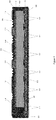
- Figure 1 illustrates a perspective view of an embodiment of a power semiconductor module having power terminals that are partially coated with an insulative material.
- Figure 2 illustrates a cross-sectional view of the power semiconductor module along the line labeled A-A' in Figure 1 .
- Figure 3 illustrates a perspective view of the power semiconductor module with the housing, internal potting compound and some internal electrical connections not shown for ease of illustration.
- the power semiconductor module includes a base plate 100 and a plurality of substrates 102 each having a bottom metallized side (out of view) attached to the base plate 100, e.g., via solder, brazing material, etc.
- the base plate 100 is thermally conductive, and can be electrically conductive or insulative.
- the base plate 100 can be a metal block or a ceramic such as Al 2 O 3 or AlN.
- Each substrate 102 has an opposing top metallized side 104, which can comprise the same or different material as the metallized bottom side.
- each substrate 102 can be a standard DCB (direct copper bonded), DAB (direct aluminum bonded), AMB (active metal brazed) or IMS (insulated metal substrate) substrate.
- a standard DCB substrate includes copper surfaces applied to the top and bottom areas of an isolation material such as Al 2 O 3 or AlN ceramic material.
- a standard DAB substrate includes aluminum surfaces applied to the top and bottom areas of a ceramic material.
- a standard AMB substrate includes metal foils brazed to opposing sides of an isolation material such as an AlN ceramic material.
- a standard IMS substrate includes an isolation material such as a polymer directly connected to the base plate 100.
- each substrate 102 can be patterned so that more than one power semiconductor die 106 can be attached to the metallized top side 104.
- all power semiconductor dies 106 can be attached to the top metallized side 104 of a single substrate.
- the power semiconductor dies 106 include one or more power semiconductor devices such as power MOSFETs, IGBTs, BJTs, thyristors, JFETs, diodes, etc. Other ones of the power semiconductor dies 106 can be passive devices such as capacitor dies and/or inductor dies.
- the power semiconductor dies 106 can be fabricated from any type of semiconductor material such as single element semiconductors (e.g. Si, Ge, etc.), silicon-on-insulator semiconductors, binary semiconductors (e.g. SiC, GaN, GaAs, etc.), ternary semiconductors, etc. with or without epitaxial layer(s).
- the power semiconductor devices are electrically connected within the module to form a power circuit such as a buck converter, boost converter, half-bridge, full-bridge, three-phase bridge, switched-mode power supply, bi-directional power converter, synchronous rectifier, etc.
- the internal electrical connections to form the desired power circuit can be provided by electrical connections 107 internal to the module such as wire bonds, metal clips, metal ribbons, etc. Most of the internal electrical connections are not shown in the figures for ease of illustration.
- the power semiconductor module also includes a plastic housing 108 attached to each substrate 102 and/or to the base plate 100.
- the plastic housing 108 can be formed by injection molding or other suitable process, and glued to the periphery of each substrate 102 and/or base plate 100.
- the plastic housing 108 is a polymer lid. The plastic housing 108 and the substrates 102 together enclose the power semiconductor dies 106.
- the power semiconductor module further includes a plurality of power terminals 110 attached to the top main face 104 of at least some of the substrates 102 at a first end 112.
- the power terminals 110 extend through the plastic housing 108 at a second end 114 to provide a point of external electrical connection for the power semiconductor dies 106 enclosed with the module.
- the power terminals 110 are illustrated as metal plates in the figures, but instead can be shaped like pins, posts, etc. In the case of metal plates, each metal plate 116 is disposed between the first and second ends 112, 114 of the respective power terminal 110, and extends in a direction generally perpendicular to the top main face 106 of the substrate(s) 102.
- the second ends 114 of the power terminals 110 are shown bent over in Figures 1 and 2 , and shown prior to bending in Figure 3 .
- the second ends 114 of the power terminals 110 need not be bent, e.g. in the case of metal pins and posts.
- the module can include additional terminals 118 such as input signal terminals, output signal terminals, etc.
- the power semiconductor module also includes a potting compound 120 in which the power semiconductor dies 106, the top main face 104 of each substrate 102 and at least part of the first end 112 of each power terminal 110 are embedded.
- a potting compound 120 in which the power semiconductor dies 106, the top main face 104 of each substrate 102 and at least part of the first end 112 of each power terminal 110 are embedded.
- Any standard potting compound suitable for high power semiconductor applications can be used, e.g., such as a thermosetting plastic, a silicone gel, etc.
- the height of the potting compound 120 is indicated by the dashed line labeled 'B' in Figures 2 and 3 . According to the embodiment illustrated in Figures 2 and 3 , the potting compound covers the lower part of each terminal metal plate 116 below the dashed line labeled 'B'. In general, the potting compound 120 may have any desired height.
- the potting compound 120 is not shown in Figure 3 , so that other aspects of the invention are more visible in this illustration.
- the power semiconductor module further includes an insulative coating 122 applied only to parts of the power terminals 110 disposed inside the plastic housing 108 and in contact with just air. As such, the insulative coating 122 is not applied to any part of the power terminals 110 disposed outside the plastic housing 108. The insulative coating 122 also is not applied to any part of the power terminals 110 disposed inside the plastic housing 108 and which are in contact with the potting compound 120 or the plastic housing 108.
- each terminal metal plate 116 is in contact with the plastic housing 108 and the lower part of each terminal metal plate 116 is embedded in the potting compound 120.
- the dashed line labeled 'C' in Figures 2 and 3 is a line of demarcation below which the plastic housing 108 does not contact the terminal metal plates 116.
- the dashed line labeled 'B' in Figures 2 and 3 is a line of demarcation above which the potting compound 120 does not contact the terminal metal plates 116.
- the region of the terminal metal plates 116 disposed between lines 'A' and 'B' is in contact with just air and thus coated with the insulative material 122.
- the insulative coating 122 is not applied to the upper part of each terminal metal plate 116 in contact with the plastic housing 108 (above line 'C' in Figures 2 and 3 ) or to the lower part of each terminal metal plate 116 embedded in the potting compound 120 (below line 'B' in Figures 2 and 3 ). Further according to this embodiment, the insulative coating 122 is not applied to the first and second ends 112, 114 of each power terminal 110.
- Figure 4 illustrates a cross-sectional view of another embodiment of a power semiconductor module having power terminals that are partially coated with an insulative material.
- the embodiment shown in Figure 4 is similar to the embodiment illustrated in Figure 2 .
- the potting compound 120 terminates before reaching the metal plate 116 of each power terminal 110.
- each terminal metal plate 116 of the power semiconductor module is completely uncovered by the potting compound 120.
- the insulative coating 122 is applied to the (lower) part of each terminal metal plate 116 nearest the potting compound 120 but not to the (upper) part of each terminal metal plate 116 in contact with the plastic housing 108.
- the dashed line labeled 'C' in Figure 4 is a line of demarcation below which the plastic housing 108 does not contact the terminal metal plates 116.
- the dashed line labeled 'B' in Figure 4 is a line of demarcation above which the potting compound 120 does not contact the terminal metal plates 116.
- the region of the terminal metal plates 116 disposed between lines 'A' and 'B' in Figure 4 is in contact with just air and thus coated with the insulative material 122. Still other potting compound fill levels (heights) are contemplated.
- FIG 5 illustrates an embodiment of a method of manufacturing the power semiconductor modules illustrated in Figures 1 through 4 .
- the method includes attaching one or more power semiconductor dies to a top main face of a substrate (Block 200).
- a plastic housing is attached to the substrate (Block 202).
- the plastic housing and the substrate together enclose the one or more power semiconductor dies.
- a plurality of power terminals is attached to the top main face of the substrate at a first end (Block 204).
- Each power terminal extends through the plastic housing at a second end to provide a point of external electrical connection for the one or more power semiconductor dies.
- Each power semiconductor die, the top main face of the substrate and at least part of the first end of each power terminal are embedded in a potting compound (Block 206).
- an insulative coating is applied only to parts of the power terminals to be disposed inside the plastic housing and in contact with just air (Block 208).
- the selectively applied insulative coating described herein can comprise one or more layers of electrically insulative material.
- the insulative coating comprises a polyimide applied only to the parts of the power terminals to be disposed inside the plastic housing and in contact with just air.
- the insulative coating comprises dried paint, a plastic material or a dried lacquer.
- the paint, plastic material or lacquer is applied only to the parts of each power terminal to be disposed inside the plastic housing and in contact with just air. The paint, plastic material or lacquer is then dried by solvent evaporation or a curing process.
- the insulative coating comprises an adhesive tape or film applied only to the parts of the power terminals to be disposed inside the plastic housing and in contact with just air.
- the insulative coating is applied by powder coating only to the parts of the power terminals to be disposed inside the plastic housing and in contact with just air.
- the parts of the power terminals not to be coated can be masked before the insulative material is applied.
- a blanket coverage of the insulative material is applied to the power terminals after the mask is applied, and the mask is then removed with the insulative material applied to the mask.
- the insulative material can be blanket deposited on the power terminals and then selectively removed from the parts of the power terminals to be disposed inside the plastic housing and in contact with the plastic housing or the potting compound.
- the insulative material can be selectively applied by a transfer printing process onto only the parts of the power terminals to be disposed inside the plastic housing and in contact with just air.
- a tape or adhesive film such as a polyimide tape can be glued only to the parts of the power terminals to be disposed inside the plastic housing and in contact with just air.
- An adhesion promoter can be used to increase the adhesive bond between the insulative coating and the power terminals.
- any standard powder coating process can be used.
- any material which can be transferred to the surface of the power terminals and has the insulating characteristic needed for the application can be used as the insulative coating described herein.
Landscapes
- Structures Or Materials For Encapsulating Or Coating Semiconductor Devices Or Solid State Devices (AREA)
- Engineering & Computer Science (AREA)
- Manufacturing & Machinery (AREA)
- Encapsulation Of And Coatings For Semiconductor Or Solid State Devices (AREA)
Abstract
Description
- The present application relates to power semiconductor modules, and particularly to power semiconductor modules with partially coated power terminals.
- A power semiconductor module provides the physical containment for several power semiconductor devices such as one or more power MOSFETs (metal-oxide-semiconductor field-effect transistors), IGBTs (insulated gate bipolar transistors), BJTs (bipolar junction transistors), thyristors, JFETs (junction field-effect transistors), diodes, etc. The power semiconductor devices are typically fabricated in one or more semiconductor dies which are attached to a power electronic substrate. A plastic housing, along with the substrate, enclose the power semiconductor devices.
- Within a power semiconductor module, sufficient isolation distances between the electric potentials must be realized to ensure proper performance, safety and reliability. Due to limited space in the inner volume of a power semiconductor module, free air does not provide sufficient isolation between components under electrical voltage.
- A soft potting isolation compound is often used to electrically insulate all exposed areas requiring electrical insulation. The filling height of the potting compound inside a power semiconductor module directly depends on the inner construction of the module. The need for fulfilling all other requirements as manufacturability of the plastic housing, processability and compatibility to existing production processes during manufacturing of a power semiconductor module generally results in higher filling heights of the potting compound, which adversely affects lifetime performance of the module. Thermal expansion of the potting material, for example, can cause substantial mechanical interactions between components with different thermal expansion coefficients, and even significant thermomechanical stress in the potting material itself. Under application conditions for an IGBT-based power semiconductor module, propagation of cracks in the potting material is a real concern which can lead to insulation failure of the module.
- Hence, there is a need for a power semiconductor module with more reliable electrical insulation.
- According to an embodiment of a power semiconductor module, the power semiconductor module comprises: one or more power semiconductor dies attached to a first main face of a substrate; a plastic housing attached to the substrate, the plastic housing and the substrate together enclosing the one or more power semiconductor dies; a plurality of power terminals attached to the first main face of the substrate at a first end, and extending through the plastic housing at a second end to provide a point of external electrical connection for the one or more power semiconductor dies; a potting compound embedding the one or more power semiconductor dies, the first main face of the substrate and at least part of the first end of the plurality of power terminals; and an insulative coating applied only to parts of the plurality of power terminals disposed inside the plastic housing and in contact with just air.
- According to an embodiment of a method of manufacturing a power semiconductor module, the method comprises: attaching one or more power semiconductor dies to a first main face of a substrate; attaching a plastic housing to the substrate, the plastic housing and the substrate together enclosing the one or more power semiconductor dies; attaching a plurality of power terminals to the first main face of the substrate at a first end, each power terminal extending through the plastic housing at a second end to provide a point of external electrical connection for the one or more power semiconductor dies; embedding the one or more power semiconductor dies, the first main face of the substrate and at least part of the first end of the plurality of power terminals in a potting compound; and prior to attaching the plurality of power terminals to the first main face of the substrate, applying an insulative coating only to parts of the plurality of power terminals to be disposed inside the plastic housing and in contact with just air.
- Those skilled in the art will recognize additional features and advantages upon reading the following detailed description, and upon viewing the accompanying drawings.
- The elements of the drawings are not necessarily to scale relative to each other. Like reference numerals designate corresponding similar parts. The features of the various illustrated embodiments can be combined unless they exclude each other. Embodiments are depicted in the drawings and are detailed in the description which follows.
-
Figure 1 illustrates a perspective view of an embodiment of a power semiconductor module having power terminals that are partially coated with an insulative material. -
Figure 2 illustrates a cross-sectional view of the power semiconductor module along the line labeled A-A' inFigure 1 . -
Figure 3 illustrates a perspective view of the power semiconductor module inFigure 1 with the housing, internal potting compound and some internal electrical connections not shown for ease of illustration. -
Figure 4 illustrates a cross-sectional view of another embodiment of a power semiconductor module having power terminals that are partially coated with an insulative material. -
Figure 5 illustrates an embodiment of a method of manufacturing the power semiconductor module. - Embodiments described herein provide a power semiconductor module having power terminals that are partially coated with an insulative material, and a corresponding method of manufacture. The insulative coating is omitted from those areas of the power terminals for realizing electrical contacts within the module and to an external busbar. Additionally, areas of the power terminals that have either direct contact to a potting compound included in the module or that are electrically isolated by plastic components of the module housing, are also not coated with the insulative material. This way, application of the insulative material to the power terminals can be selectively optimized with respect to the physical conditions and layer thicknesses of the module. Furthermore, the height of the potting compound inside the module can be reduced, decreasing the likelihood of thermomechanical damage to the potting compound within the module.
-
Figure 1 illustrates a perspective view of an embodiment of a power semiconductor module having power terminals that are partially coated with an insulative material. -
Figure 2 illustrates a cross-sectional view of the power semiconductor module along the line labeled A-A' inFigure 1 . -
Figure 3 illustrates a perspective view of the power semiconductor module with the housing, internal potting compound and some internal electrical connections not shown for ease of illustration. - The power semiconductor module includes a
base plate 100 and a plurality ofsubstrates 102 each having a bottom metallized side (out of view) attached to thebase plate 100, e.g., via solder, brazing material, etc. Thebase plate 100 is thermally conductive, and can be electrically conductive or insulative. For example, thebase plate 100 can be a metal block or a ceramic such as Al2O3 or AlN. - Each
substrate 102 has an opposing topmetallized side 104, which can comprise the same or different material as the metallized bottom side. For example, eachsubstrate 102 can be a standard DCB (direct copper bonded), DAB (direct aluminum bonded), AMB (active metal brazed) or IMS (insulated metal substrate) substrate. A standard DCB substrate includes copper surfaces applied to the top and bottom areas of an isolation material such as Al2O3 or AlN ceramic material. A standard DAB substrate includes aluminum surfaces applied to the top and bottom areas of a ceramic material. A standard AMB substrate includes metal foils brazed to opposing sides of an isolation material such as an AlN ceramic material. A standard IMS substrate includes an isolation material such as a polymer directly connected to thebase plate 100. In each case, the metallizedtop side 104 of eachsubstrate 102 can be patterned so that more than onepower semiconductor die 106 can be attached to the metallizedtop side 104. Instead of multiple substrates, all power semiconductor dies 106 can be attached to the topmetallized side 104 of a single substrate. - At least some of the power semiconductor dies 106 include one or more power semiconductor devices such as power MOSFETs, IGBTs, BJTs, thyristors, JFETs, diodes, etc. Other ones of the power semiconductor dies 106 can be passive devices such as capacitor dies and/or inductor dies. The power semiconductor dies 106 can be fabricated from any type of semiconductor material such as single element semiconductors (e.g. Si, Ge, etc.), silicon-on-insulator semiconductors, binary semiconductors (e.g. SiC, GaN, GaAs, etc.), ternary semiconductors, etc. with or without epitaxial layer(s).
- The power semiconductor devices are electrically connected within the module to form a power circuit such as a buck converter, boost converter, half-bridge, full-bridge, three-phase bridge, switched-mode power supply, bi-directional power converter, synchronous rectifier, etc. The internal electrical connections to form the desired power circuit can be provided by
electrical connections 107 internal to the module such as wire bonds, metal clips, metal ribbons, etc. Most of the internal electrical connections are not shown in the figures for ease of illustration. - The power semiconductor module also includes a
plastic housing 108 attached to eachsubstrate 102 and/or to thebase plate 100. Theplastic housing 108 can be formed by injection molding or other suitable process, and glued to the periphery of eachsubstrate 102 and/orbase plate 100. In one embodiment, theplastic housing 108 is a polymer lid. Theplastic housing 108 and thesubstrates 102 together enclose the power semiconductor dies 106. - The power semiconductor module further includes a plurality of
power terminals 110 attached to the topmain face 104 of at least some of thesubstrates 102 at afirst end 112. Thepower terminals 110 extend through theplastic housing 108 at asecond end 114 to provide a point of external electrical connection for the power semiconductor dies 106 enclosed with the module. Thepower terminals 110 are illustrated as metal plates in the figures, but instead can be shaped like pins, posts, etc. In the case of metal plates, eachmetal plate 116 is disposed between the first andsecond ends respective power terminal 110, and extends in a direction generally perpendicular to the topmain face 106 of the substrate(s) 102. Thesecond ends 114 of thepower terminals 110 are shown bent over inFigures 1 and2 , and shown prior to bending inFigure 3 . Thesecond ends 114 of thepower terminals 110 need not be bent, e.g. in the case of metal pins and posts. The module can includeadditional terminals 118 such as input signal terminals, output signal terminals, etc. - The power semiconductor module also includes a
potting compound 120 in which the power semiconductor dies 106, the topmain face 104 of eachsubstrate 102 and at least part of thefirst end 112 of eachpower terminal 110 are embedded. Any standard potting compound suitable for high power semiconductor applications can be used, e.g., such as a thermosetting plastic, a silicone gel, etc. The height of thepotting compound 120 is indicated by the dashed line labeled 'B' inFigures 2 and3 . According to the embodiment illustrated inFigures 2 and3 , the potting compound covers the lower part of eachterminal metal plate 116 below the dashed line labeled 'B'. In general, thepotting compound 120 may have any desired height. Thepotting compound 120 is not shown inFigure 3 , so that other aspects of the invention are more visible in this illustration. - The power semiconductor module further includes an
insulative coating 122 applied only to parts of thepower terminals 110 disposed inside theplastic housing 108 and in contact with just air. As such, theinsulative coating 122 is not applied to any part of thepower terminals 110 disposed outside theplastic housing 108. Theinsulative coating 122 also is not applied to any part of thepower terminals 110 disposed inside theplastic housing 108 and which are in contact with thepotting compound 120 or theplastic housing 108. - In the embodiment illustrated in
Figures 2 and3 , the upper part of eachterminal metal plate 116 is in contact with theplastic housing 108 and the lower part of eachterminal metal plate 116 is embedded in thepotting compound 120. The dashed line labeled 'C' inFigures 2 and3 is a line of demarcation below which theplastic housing 108 does not contact theterminal metal plates 116. Likewise, the dashed line labeled 'B' inFigures 2 and3 is a line of demarcation above which thepotting compound 120 does not contact theterminal metal plates 116. The region of theterminal metal plates 116 disposed between lines 'A' and 'B' is in contact with just air and thus coated with theinsulative material 122. Theinsulative coating 122 is not applied to the upper part of eachterminal metal plate 116 in contact with the plastic housing 108 (above line 'C' inFigures 2 and3 ) or to the lower part of eachterminal metal plate 116 embedded in the potting compound 120 (below line 'B' inFigures 2 and3 ). Further according to this embodiment, theinsulative coating 122 is not applied to the first and second ends 112, 114 of eachpower terminal 110. -
Figure 4 illustrates a cross-sectional view of another embodiment of a power semiconductor module having power terminals that are partially coated with an insulative material. The embodiment shown inFigure 4 is similar to the embodiment illustrated inFigure 2 . Different, however, thepotting compound 120 terminates before reaching themetal plate 116 of eachpower terminal 110. As such, eachterminal metal plate 116 of the power semiconductor module is completely uncovered by thepotting compound 120. According to this embodiment, theinsulative coating 122 is applied to the (lower) part of eachterminal metal plate 116 nearest thepotting compound 120 but not to the (upper) part of eachterminal metal plate 116 in contact with theplastic housing 108. The dashed line labeled 'C' inFigure 4 is a line of demarcation below which theplastic housing 108 does not contact theterminal metal plates 116. Likewise, the dashed line labeled 'B' inFigure 4 is a line of demarcation above which thepotting compound 120 does not contact theterminal metal plates 116. The region of theterminal metal plates 116 disposed between lines 'A' and 'B' inFigure 4 is in contact with just air and thus coated with theinsulative material 122. Still other potting compound fill levels (heights) are contemplated. -
Figure 5 illustrates an embodiment of a method of manufacturing the power semiconductor modules illustrated inFigures 1 through 4 . The method includes attaching one or more power semiconductor dies to a top main face of a substrate (Block 200). A plastic housing is attached to the substrate (Block 202). The plastic housing and the substrate together enclose the one or more power semiconductor dies. A plurality of power terminals is attached to the top main face of the substrate at a first end (Block 204). Each power terminal extends through the plastic housing at a second end to provide a point of external electrical connection for the one or more power semiconductor dies. Each power semiconductor die, the top main face of the substrate and at least part of the first end of each power terminal are embedded in a potting compound (Block 206). Prior to attaching the power terminals to the first main face of the substrate, an insulative coating is applied only to parts of the power terminals to be disposed inside the plastic housing and in contact with just air (Block 208). - The selectively applied insulative coating described herein can comprise one or more layers of electrically insulative material. In one embodiment, the insulative coating comprises a polyimide applied only to the parts of the power terminals to be disposed inside the plastic housing and in contact with just air.
- In addition or alternatively, the insulative coating comprises dried paint, a plastic material or a dried lacquer. According to this embodiment, the paint, plastic material or lacquer is applied only to the parts of each power terminal to be disposed inside the plastic housing and in contact with just air. The paint, plastic material or lacquer is then dried by solvent evaporation or a curing process.
- In addition or alternatively, the insulative coating comprises an adhesive tape or film applied only to the parts of the power terminals to be disposed inside the plastic housing and in contact with just air.
- In addition or alternatively, the insulative coating is applied by powder coating only to the parts of the power terminals to be disposed inside the plastic housing and in contact with just air.
- Yet other coating methods can be used, depending on the type of insulative coating.
- In the case of the insulative material being applied as a solvent and then dried such as the case with paint, a plastic material, spray-on lacquer, etc., the parts of the power terminals not to be coated can be masked before the insulative material is applied. A blanket coverage of the insulative material is applied to the power terminals after the mask is applied, and the mask is then removed with the insulative material applied to the mask. In another embodiment, the insulative material can be blanket deposited on the power terminals and then selectively removed from the parts of the power terminals to be disposed inside the plastic housing and in contact with the plastic housing or the potting compound. In yet another embodiment, the insulative material can be selectively applied by a transfer printing process onto only the parts of the power terminals to be disposed inside the plastic housing and in contact with just air.
- In the case of the insulative material being applied as a glue or foil, a tape or adhesive film such as a polyimide tape can be glued only to the parts of the power terminals to be disposed inside the plastic housing and in contact with just air. An adhesion promoter can be used to increase the adhesive bond between the insulative coating and the power terminals.
- In the case of the insulative material being applied by powder coating, any standard powder coating process can be used.
- In general, any material which can be transferred to the surface of the power terminals and has the insulating characteristic needed for the application can be used as the insulative coating described herein.
- Spatially relative terms such as "under", "below", "lower", "over", "upper" and the like, are used for ease of description to explain the positioning of one element relative to a second element. These terms are intended to encompass different orientations of the device in addition to different orientations than those depicted in the figures. Further, terms such as "first", "second", and the like, are also used to describe various elements, regions, sections, etc. and are also not intended to be limiting. Like terms refer to like elements throughout the description.
- As used herein, the terms "having", "containing", "including", "comprising" and the like are open ended terms that indicate the presence of stated elements or features, but do not preclude additional elements or features. The articles "a", "an" and "the" are intended to include the plural as well as the singular, unless the context clearly indicates otherwise.
- With the above range of variations and applications in mind, it should be understood that the present invention is not limited by the foregoing description, nor is it limited by the accompanying drawings. Instead, the present invention is limited only by the following claims and their legal equivalents.
Claims (15)
- A power semiconductor module, comprising:one or more power semiconductor dies attached to a first main face of a substrate;a plastic housing attached to the substrate, the plastic housing and the substrate together enclosing the one or more power semiconductor dies;a plurality of power terminals attached to the first main face of the substrate at a first end, and extending through the plastic housing at a second end to provide a point of external electrical connection for the one or more power semiconductor dies;a potting compound embedding the one or more power semiconductor dies, the first main face of the substrate and at least part of the first end of the plurality of power terminals; andan insulative coating applied only to parts of the plurality of power terminals disposed inside the plastic housing and in contact with just air.
- The power semiconductor module of claim 1, wherein the potting compound comprises a thermosetting plastic or a silicone gel.
- The power semiconductor module of claim 1 or 2, wherein one of the following applies:the insulative coating comprises a polyimide;the insulative coating comprises dried paint, a plastic material or a dried lacquer;the insulative coating comprises an adhesive tape or film; andthe insulative coating comprises a powder coating.
- The power semiconductor module of any of claims 1 to 3, wherein each power terminal of the plurality of power terminals comprises a metal plate between the first and the second ends of the power terminal, the metal plate extending in a direction generally perpendicular to the first main face of the substrate.
- The power semiconductor module of claim 4, wherein the potting compound terminates before reaching the metal plate of each power terminal of the plurality of power terminals so that each metal plate is completely uncovered by the potting compound.
- The power semiconductor module of claim 4 or 5, wherein the insulative coating is applied to a first part of each metal plate nearest the potting compound but not to a second part of each metal plate above the first part and in contact with the plastic housing.
- A method of manufacturing a power semiconductor module, the method comprising:attaching one or more power semiconductor dies to a first main face of a substrate;attaching a plastic housing to the substrate, the plastic housing and the substrate together enclosing the one or more power semiconductor dies;attaching a plurality of power terminals to the first main face of the substrate at a first end, each power terminal extending through the plastic housing at a second end to provide a point of external electrical connection for the one or more power semiconductor dies;embedding the one or more power semiconductor dies, the first main face of the substrate and at least part of the first end of the plurality of power terminals in a potting compound; andprior to attaching the plurality of power terminals to the first main face of the substrate, applying an insulative coating only to parts of the plurality of power terminals to be disposed inside the plastic housing and in contact with just air.
- The method of claim 7, wherein applying the insulative coating only to parts of the plurality of power terminals to be disposed inside the plastic housing and in contact with just air comprises:applying polyimide only to the parts of the plurality of power terminals to be disposed inside the plastic housing and in contact with just air.
- The method of claim 7, wherein applying the insulative coating only to parts of the plurality of power terminals to be disposed inside the plastic housing and in contact with just air comprises:applying paint, a plastic material or a lacquer only to the parts of the plurality of power terminals to be disposed inside the plastic housing and in contact with just air; anddrying the paint, plastic material or lacquer by solvent evaporation or a curing process.
- The method of claim 7, wherein applying the insulative coating only to parts of the plurality of power terminals to be disposed inside the plastic housing and in contact with just air comprises one of the following:applying an adhesive tape or film only to the parts of the plurality of power terminals to be disposed inside the plastic housing and in contact with just air;powder coating only the parts of the plurality of power terminals to be disposed inside the plastic housing and in contact with just air; andtransfer printing an insulative material onto only the parts of the plurality of power terminals to be disposed inside the plastic housing and in contact with just air.
- The method of claim 7, wherein applying the insulative coating only to parts of the plurality of power terminals to be disposed inside the plastic housing and in contact with just air comprises:applying a blanket coverage of insulative material to the plurality of power terminals; andremoving the insulative material from parts of the plurality of power terminals to be disposed inside the plastic housing and in contact with the plastic housing or the potting compound.
- The method of claim 7, wherein applying the insulative coating only to parts of the plurality of power terminals to be disposed inside the plastic housing and in contact with just air comprises:applying a mask to the parts of the plurality of power terminals to be disposed inside the plastic housing and in contact with just air;applying a blanket coverage of insulative material to the plurality of power terminals after the mask is applied; andremoving the mask with the insulative material applied to the mask.
- The method of any of claims 7 to 12, wherein each power terminal of the plurality of power terminals comprises a metal plate between the first and the second ends of the power terminal, the metal plate extending in a direction generally perpendicular to the first main face of the substrate.
- The method of claim 13, further comprising:terminating the potting compound before the potting compound reaches the metal plate of each power terminal of the plurality of power terminals, so that each metal plate is completely uncovered by the potting compound.
- The method of claim 13 or 14, wherein applying the insulative coating only to parts of the plurality of power terminals to be disposed inside the plastic housing and in contact with just air comprises:applying the insulative coating to a first part of each metal plate to be disposed nearest the potting compound, but not to a second part of each metal plate above the first part and to be in contact with the plastic housing.
Applications Claiming Priority (1)
| Application Number | Priority Date | Filing Date | Title |
|---|---|---|---|
| US15/795,077 US10283447B1 (en) | 2017-10-26 | 2017-10-26 | Power semiconductor module with partially coated power terminals and method of manufacturing thereof |
Publications (2)
| Publication Number | Publication Date |
|---|---|
| EP3477694A1 true EP3477694A1 (en) | 2019-05-01 |
| EP3477694B1 EP3477694B1 (en) | 2020-12-09 |
Family
ID=64082875
Family Applications (1)
| Application Number | Title | Priority Date | Filing Date |
|---|---|---|---|
| EP18202737.5A Active EP3477694B1 (en) | 2017-10-26 | 2018-10-26 | Power semiconductor module with partially coated power terminals |
Country Status (3)
| Country | Link |
|---|---|
| US (1) | US10283447B1 (en) |
| EP (1) | EP3477694B1 (en) |
| CN (1) | CN109712944A (en) |
Families Citing this family (3)
| Publication number | Priority date | Publication date | Assignee | Title |
|---|---|---|---|---|
| EP3518278A1 (en) * | 2018-01-30 | 2019-07-31 | Infineon Technologies AG | Power semiconductor module and method for producing the same |
| DE102021206935B4 (en) * | 2021-07-01 | 2024-01-25 | Vitesco Technologies Germany Gmbh | Power half-bridge module, power inverter, method for producing a power half-bridge module |
| EP4560702A1 (en) | 2023-11-26 | 2025-05-28 | Bayerische Motoren Werke Aktiengesellschaft | Power module and the process of producing a power module |
Citations (4)
| Publication number | Priority date | Publication date | Assignee | Title |
|---|---|---|---|---|
| JP2000216332A (en) * | 1999-01-20 | 2000-08-04 | Hitachi Ltd | Semiconductor device |
| JP2002217362A (en) * | 2001-01-12 | 2002-08-02 | Yazaki Corp | Semiconductor device |
| US20150001700A1 (en) * | 2013-06-28 | 2015-01-01 | Infineon Technologies Ag | Power Modules with Parylene Coating |
| DE102014104856A1 (en) * | 2014-04-04 | 2015-10-08 | Infineon Technologies Ag | Explosion-proof power semiconductor module |
Family Cites Families (11)
| Publication number | Priority date | Publication date | Assignee | Title |
|---|---|---|---|---|
| CN1146988C (en) * | 1997-12-08 | 2004-04-21 | 东芝株式会社 | Package for semiconductor power device and method for assembling the same |
| DE102006027481C5 (en) | 2006-06-14 | 2012-11-08 | Semikron Elektronik Gmbh & Co. Kg | Power semiconductor module with mutually electrically insulated connection elements |
| US8674462B2 (en) * | 2007-07-25 | 2014-03-18 | Infineon Technologies Ag | Sensor package |
| US8018047B2 (en) * | 2007-08-06 | 2011-09-13 | Infineon Technologies Ag | Power semiconductor module including a multilayer substrate |
| DE102009046858B3 (en) * | 2009-11-19 | 2011-05-05 | Infineon Technologies Ag | Power semiconductor module and method for operating a power semiconductor module |
| US8446726B2 (en) * | 2010-10-28 | 2013-05-21 | Infineon Technologies Ag | Semiconductor module having an insert and method for producing a semiconductor module having an insert |
| DE102012222015B4 (en) * | 2012-11-30 | 2019-07-18 | Infineon Technologies Ag | Moisture-proof semiconductor module and a method for its production |
| DE102013219833B4 (en) * | 2013-09-30 | 2020-02-13 | Infineon Technologies Ag | SEMICONDUCTOR MODULE WITH CIRCUIT BOARD AND METHOD FOR PRODUCING A SEMICONDUCTOR MODULE WITH A CIRCUIT BOARD |
| JP6330436B2 (en) * | 2014-04-01 | 2018-05-30 | 富士電機株式会社 | Power semiconductor module |
| JP6233507B2 (en) * | 2014-05-15 | 2017-11-22 | 富士電機株式会社 | Power semiconductor modules and composite modules |
| US9443792B1 (en) * | 2015-10-31 | 2016-09-13 | Ixys Corporation | Bridging DMB structure for wire bonding in a power semiconductor device module |
-
2017
- 2017-10-26 US US15/795,077 patent/US10283447B1/en active Active
-
2018
- 2018-10-25 CN CN201811251193.2A patent/CN109712944A/en active Pending
- 2018-10-26 EP EP18202737.5A patent/EP3477694B1/en active Active
Patent Citations (4)
| Publication number | Priority date | Publication date | Assignee | Title |
|---|---|---|---|---|
| JP2000216332A (en) * | 1999-01-20 | 2000-08-04 | Hitachi Ltd | Semiconductor device |
| JP2002217362A (en) * | 2001-01-12 | 2002-08-02 | Yazaki Corp | Semiconductor device |
| US20150001700A1 (en) * | 2013-06-28 | 2015-01-01 | Infineon Technologies Ag | Power Modules with Parylene Coating |
| DE102014104856A1 (en) * | 2014-04-04 | 2015-10-08 | Infineon Technologies Ag | Explosion-proof power semiconductor module |
Also Published As
| Publication number | Publication date |
|---|---|
| US20190131234A1 (en) | 2019-05-02 |
| EP3477694B1 (en) | 2020-12-09 |
| CN109712944A (en) | 2019-05-03 |
| US10283447B1 (en) | 2019-05-07 |
Similar Documents
| Publication | Publication Date | Title |
|---|---|---|
| US11239132B2 (en) | Semiconductor power device with corresponding package and related manufacturing process | |
| US7759778B2 (en) | Leaded semiconductor power module with direct bonding and double sided cooling | |
| CN105874596B (en) | semiconductor module | |
| US11362008B2 (en) | Power semiconductor module embedded in a mold compounded with an opening | |
| CN104517913A (en) | Semiconductor device and method for manufacturing the same | |
| US20070257343A1 (en) | Die-on-leadframe (dol) with high voltage isolation | |
| JP4465906B2 (en) | Power semiconductor module | |
| US10854524B2 (en) | Power semiconductor module | |
| WO2015174158A1 (en) | Power semiconductor module and composite module | |
| JP4967701B2 (en) | Power semiconductor device | |
| EP3477694B1 (en) | Power semiconductor module with partially coated power terminals | |
| JP3440824B2 (en) | Semiconductor device | |
| US20150249067A1 (en) | Semiconductor Device Having Multiple Chips Mounted to a Carrier | |
| US9379050B2 (en) | Electronic device | |
| US8829692B2 (en) | Multilayer packaged semiconductor device and method of packaging | |
| EP3863045A1 (en) | Power semiconductor module arrangement and method for producing the same | |
| US11776940B2 (en) | Electronic power module | |
| JP2025074405A (en) | Semiconductor module and method for manufacturing the same | |
| CN116895628A (en) | Semiconductor package module with vertical terminals | |
| US20250054840A1 (en) | Power module having a lead frame that provides substrate support and forms terminals of the power module | |
| US12482725B2 (en) | Power semiconductor module arrangements and methods for producing power semiconductor module arrangements | |
| US20250218914A1 (en) | Package with component-carrying intermediate structure and additional carrier having reference potential structure | |
| US11404392B1 (en) | Molded semiconductor module for PCB embedding | |
| US20260047509A1 (en) | Electronic Device Having Pins with a Bent Profile | |
| US20250285937A1 (en) | Housing, semiconductor module comprising a housing, and method for assembling a semiconductor module |
Legal Events
| Date | Code | Title | Description |
|---|---|---|---|
| PUAI | Public reference made under article 153(3) epc to a published international application that has entered the european phase |
Free format text: ORIGINAL CODE: 0009012 |
|
| STAA | Information on the status of an ep patent application or granted ep patent |
Free format text: STATUS: THE APPLICATION HAS BEEN PUBLISHED |
|
| AK | Designated contracting states |
Kind code of ref document: A1 Designated state(s): AL AT BE BG CH CY CZ DE DK EE ES FI FR GB GR HR HU IE IS IT LI LT LU LV MC MK MT NL NO PL PT RO RS SE SI SK SM TR |
|
| AX | Request for extension of the european patent |
Extension state: BA ME |
|
| STAA | Information on the status of an ep patent application or granted ep patent |
Free format text: STATUS: REQUEST FOR EXAMINATION WAS MADE |
|
| 17P | Request for examination filed |
Effective date: 20191031 |
|
| RBV | Designated contracting states (corrected) |
Designated state(s): AL AT BE BG CH CY CZ DE DK EE ES FI FR GB GR HR HU IE IS IT LI LT LU LV MC MK MT NL NO PL PT RO RS SE SI SK SM TR |
|
| RIC1 | Information provided on ipc code assigned before grant |
Ipc: H01L 23/053 20060101ALI20200602BHEP Ipc: H01L 23/24 20060101AFI20200602BHEP Ipc: H01L 25/18 20060101ALI20200602BHEP Ipc: H01L 25/07 20060101ALI20200602BHEP |
|
| GRAP | Despatch of communication of intention to grant a patent |
Free format text: ORIGINAL CODE: EPIDOSNIGR1 |
|
| STAA | Information on the status of an ep patent application or granted ep patent |
Free format text: STATUS: GRANT OF PATENT IS INTENDED |
|
| INTG | Intention to grant announced |
Effective date: 20200714 |
|
| GRAS | Grant fee paid |
Free format text: ORIGINAL CODE: EPIDOSNIGR3 |
|
| GRAA | (expected) grant |
Free format text: ORIGINAL CODE: 0009210 |
|
| STAA | Information on the status of an ep patent application or granted ep patent |
Free format text: STATUS: THE PATENT HAS BEEN GRANTED |
|
| AK | Designated contracting states |
Kind code of ref document: B1 Designated state(s): AL AT BE BG CH CY CZ DE DK EE ES FI FR GB GR HR HU IE IS IT LI LT LU LV MC MK MT NL NO PL PT RO RS SE SI SK SM TR |
|
| REG | Reference to a national code |
Ref country code: GB Ref legal event code: FG4D |
|
| REG | Reference to a national code |
Ref country code: AT Ref legal event code: REF Ref document number: 1344264 Country of ref document: AT Kind code of ref document: T Effective date: 20201215 Ref country code: CH Ref legal event code: EP |
|
| REG | Reference to a national code |
Ref country code: DE Ref legal event code: R096 Ref document number: 602018010607 Country of ref document: DE |
|
| REG | Reference to a national code |
Ref country code: IE Ref legal event code: FG4D |
|
| PG25 | Lapsed in a contracting state [announced via postgrant information from national office to epo] |
Ref country code: GR Free format text: LAPSE BECAUSE OF FAILURE TO SUBMIT A TRANSLATION OF THE DESCRIPTION OR TO PAY THE FEE WITHIN THE PRESCRIBED TIME-LIMIT Effective date: 20210310 Ref country code: NO Free format text: LAPSE BECAUSE OF FAILURE TO SUBMIT A TRANSLATION OF THE DESCRIPTION OR TO PAY THE FEE WITHIN THE PRESCRIBED TIME-LIMIT Effective date: 20210309 Ref country code: FI Free format text: LAPSE BECAUSE OF FAILURE TO SUBMIT A TRANSLATION OF THE DESCRIPTION OR TO PAY THE FEE WITHIN THE PRESCRIBED TIME-LIMIT Effective date: 20201209 Ref country code: RS Free format text: LAPSE BECAUSE OF FAILURE TO SUBMIT A TRANSLATION OF THE DESCRIPTION OR TO PAY THE FEE WITHIN THE PRESCRIBED TIME-LIMIT Effective date: 20201209 |
|
| REG | Reference to a national code |
Ref country code: AT Ref legal event code: MK05 Ref document number: 1344264 Country of ref document: AT Kind code of ref document: T Effective date: 20201209 |
|
| PG25 | Lapsed in a contracting state [announced via postgrant information from national office to epo] |
Ref country code: BG Free format text: LAPSE BECAUSE OF FAILURE TO SUBMIT A TRANSLATION OF THE DESCRIPTION OR TO PAY THE FEE WITHIN THE PRESCRIBED TIME-LIMIT Effective date: 20210309 Ref country code: LV Free format text: LAPSE BECAUSE OF FAILURE TO SUBMIT A TRANSLATION OF THE DESCRIPTION OR TO PAY THE FEE WITHIN THE PRESCRIBED TIME-LIMIT Effective date: 20201209 Ref country code: SE Free format text: LAPSE BECAUSE OF FAILURE TO SUBMIT A TRANSLATION OF THE DESCRIPTION OR TO PAY THE FEE WITHIN THE PRESCRIBED TIME-LIMIT Effective date: 20201209 |
|
| REG | Reference to a national code |
Ref country code: NL Ref legal event code: MP Effective date: 20201209 |
|
| PG25 | Lapsed in a contracting state [announced via postgrant information from national office to epo] |
Ref country code: NL Free format text: LAPSE BECAUSE OF FAILURE TO SUBMIT A TRANSLATION OF THE DESCRIPTION OR TO PAY THE FEE WITHIN THE PRESCRIBED TIME-LIMIT Effective date: 20201209 Ref country code: HR Free format text: LAPSE BECAUSE OF FAILURE TO SUBMIT A TRANSLATION OF THE DESCRIPTION OR TO PAY THE FEE WITHIN THE PRESCRIBED TIME-LIMIT Effective date: 20201209 |
|
| REG | Reference to a national code |
Ref country code: LT Ref legal event code: MG9D |
|
| PG25 | Lapsed in a contracting state [announced via postgrant information from national office to epo] |
Ref country code: CZ Free format text: LAPSE BECAUSE OF FAILURE TO SUBMIT A TRANSLATION OF THE DESCRIPTION OR TO PAY THE FEE WITHIN THE PRESCRIBED TIME-LIMIT Effective date: 20201209 Ref country code: EE Free format text: LAPSE BECAUSE OF FAILURE TO SUBMIT A TRANSLATION OF THE DESCRIPTION OR TO PAY THE FEE WITHIN THE PRESCRIBED TIME-LIMIT Effective date: 20201209 Ref country code: SM Free format text: LAPSE BECAUSE OF FAILURE TO SUBMIT A TRANSLATION OF THE DESCRIPTION OR TO PAY THE FEE WITHIN THE PRESCRIBED TIME-LIMIT Effective date: 20201209 Ref country code: SK Free format text: LAPSE BECAUSE OF FAILURE TO SUBMIT A TRANSLATION OF THE DESCRIPTION OR TO PAY THE FEE WITHIN THE PRESCRIBED TIME-LIMIT Effective date: 20201209 Ref country code: RO Free format text: LAPSE BECAUSE OF FAILURE TO SUBMIT A TRANSLATION OF THE DESCRIPTION OR TO PAY THE FEE WITHIN THE PRESCRIBED TIME-LIMIT Effective date: 20201209 Ref country code: PT Free format text: LAPSE BECAUSE OF FAILURE TO SUBMIT A TRANSLATION OF THE DESCRIPTION OR TO PAY THE FEE WITHIN THE PRESCRIBED TIME-LIMIT Effective date: 20210409 Ref country code: LT Free format text: LAPSE BECAUSE OF FAILURE TO SUBMIT A TRANSLATION OF THE DESCRIPTION OR TO PAY THE FEE WITHIN THE PRESCRIBED TIME-LIMIT Effective date: 20201209 |
|
| PG25 | Lapsed in a contracting state [announced via postgrant information from national office to epo] |
Ref country code: PL Free format text: LAPSE BECAUSE OF FAILURE TO SUBMIT A TRANSLATION OF THE DESCRIPTION OR TO PAY THE FEE WITHIN THE PRESCRIBED TIME-LIMIT Effective date: 20201209 Ref country code: AT Free format text: LAPSE BECAUSE OF FAILURE TO SUBMIT A TRANSLATION OF THE DESCRIPTION OR TO PAY THE FEE WITHIN THE PRESCRIBED TIME-LIMIT Effective date: 20201209 |
|
| REG | Reference to a national code |
Ref country code: DE Ref legal event code: R097 Ref document number: 602018010607 Country of ref document: DE |
|
| PG25 | Lapsed in a contracting state [announced via postgrant information from national office to epo] |
Ref country code: IS Free format text: LAPSE BECAUSE OF FAILURE TO SUBMIT A TRANSLATION OF THE DESCRIPTION OR TO PAY THE FEE WITHIN THE PRESCRIBED TIME-LIMIT Effective date: 20210409 |
|
| PLBE | No opposition filed within time limit |
Free format text: ORIGINAL CODE: 0009261 |
|
| STAA | Information on the status of an ep patent application or granted ep patent |
Free format text: STATUS: NO OPPOSITION FILED WITHIN TIME LIMIT |
|
| PG25 | Lapsed in a contracting state [announced via postgrant information from national office to epo] |
Ref country code: AL Free format text: LAPSE BECAUSE OF FAILURE TO SUBMIT A TRANSLATION OF THE DESCRIPTION OR TO PAY THE FEE WITHIN THE PRESCRIBED TIME-LIMIT Effective date: 20201209 Ref country code: IT Free format text: LAPSE BECAUSE OF FAILURE TO SUBMIT A TRANSLATION OF THE DESCRIPTION OR TO PAY THE FEE WITHIN THE PRESCRIBED TIME-LIMIT Effective date: 20201209 |
|
| 26N | No opposition filed |
Effective date: 20210910 |
|
| PG25 | Lapsed in a contracting state [announced via postgrant information from national office to epo] |
Ref country code: DK Free format text: LAPSE BECAUSE OF FAILURE TO SUBMIT A TRANSLATION OF THE DESCRIPTION OR TO PAY THE FEE WITHIN THE PRESCRIBED TIME-LIMIT Effective date: 20201209 Ref country code: SI Free format text: LAPSE BECAUSE OF FAILURE TO SUBMIT A TRANSLATION OF THE DESCRIPTION OR TO PAY THE FEE WITHIN THE PRESCRIBED TIME-LIMIT Effective date: 20201209 |
|
| PG25 | Lapsed in a contracting state [announced via postgrant information from national office to epo] |
Ref country code: ES Free format text: LAPSE BECAUSE OF FAILURE TO SUBMIT A TRANSLATION OF THE DESCRIPTION OR TO PAY THE FEE WITHIN THE PRESCRIBED TIME-LIMIT Effective date: 20201209 |
|
| REG | Reference to a national code |
Ref country code: CH Ref legal event code: PL |
|
| PG25 | Lapsed in a contracting state [announced via postgrant information from national office to epo] |
Ref country code: IS Free format text: LAPSE BECAUSE OF FAILURE TO SUBMIT A TRANSLATION OF THE DESCRIPTION OR TO PAY THE FEE WITHIN THE PRESCRIBED TIME-LIMIT Effective date: 20210409 |
|
| REG | Reference to a national code |
Ref country code: BE Ref legal event code: MM Effective date: 20211031 |
|
| PG25 | Lapsed in a contracting state [announced via postgrant information from national office to epo] |
Ref country code: MC Free format text: LAPSE BECAUSE OF FAILURE TO SUBMIT A TRANSLATION OF THE DESCRIPTION OR TO PAY THE FEE WITHIN THE PRESCRIBED TIME-LIMIT Effective date: 20201209 |
|
| PG25 | Lapsed in a contracting state [announced via postgrant information from national office to epo] |
Ref country code: LU Free format text: LAPSE BECAUSE OF NON-PAYMENT OF DUE FEES Effective date: 20211026 Ref country code: BE Free format text: LAPSE BECAUSE OF NON-PAYMENT OF DUE FEES Effective date: 20211031 |
|
| PG25 | Lapsed in a contracting state [announced via postgrant information from national office to epo] |
Ref country code: LI Free format text: LAPSE BECAUSE OF NON-PAYMENT OF DUE FEES Effective date: 20211031 Ref country code: CH Free format text: LAPSE BECAUSE OF NON-PAYMENT OF DUE FEES Effective date: 20211031 |
|
| PG25 | Lapsed in a contracting state [announced via postgrant information from national office to epo] |
Ref country code: FR Free format text: LAPSE BECAUSE OF NON-PAYMENT OF DUE FEES Effective date: 20211031 |
|
| PG25 | Lapsed in a contracting state [announced via postgrant information from national office to epo] |
Ref country code: IE Free format text: LAPSE BECAUSE OF NON-PAYMENT OF DUE FEES Effective date: 20211026 |
|
| GBPC | Gb: european patent ceased through non-payment of renewal fee |
Effective date: 20221026 |
|
| PG25 | Lapsed in a contracting state [announced via postgrant information from national office to epo] |
Ref country code: CY Free format text: LAPSE BECAUSE OF FAILURE TO SUBMIT A TRANSLATION OF THE DESCRIPTION OR TO PAY THE FEE WITHIN THE PRESCRIBED TIME-LIMIT Effective date: 20201209 |
|
| P01 | Opt-out of the competence of the unified patent court (upc) registered |
Effective date: 20230528 |
|
| PG25 | Lapsed in a contracting state [announced via postgrant information from national office to epo] |
Ref country code: HU Free format text: LAPSE BECAUSE OF FAILURE TO SUBMIT A TRANSLATION OF THE DESCRIPTION OR TO PAY THE FEE WITHIN THE PRESCRIBED TIME-LIMIT; INVALID AB INITIO Effective date: 20181026 |
|
| PG25 | Lapsed in a contracting state [announced via postgrant information from national office to epo] |
Ref country code: GB Free format text: LAPSE BECAUSE OF NON-PAYMENT OF DUE FEES Effective date: 20221026 |
|
| PG25 | Lapsed in a contracting state [announced via postgrant information from national office to epo] |
Ref country code: MK Free format text: LAPSE BECAUSE OF FAILURE TO SUBMIT A TRANSLATION OF THE DESCRIPTION OR TO PAY THE FEE WITHIN THE PRESCRIBED TIME-LIMIT Effective date: 20201209 |
|
| PG25 | Lapsed in a contracting state [announced via postgrant information from national office to epo] |
Ref country code: TR Free format text: LAPSE BECAUSE OF FAILURE TO SUBMIT A TRANSLATION OF THE DESCRIPTION OR TO PAY THE FEE WITHIN THE PRESCRIBED TIME-LIMIT Effective date: 20201209 |
|
| PG25 | Lapsed in a contracting state [announced via postgrant information from national office to epo] |
Ref country code: MT Free format text: LAPSE BECAUSE OF FAILURE TO SUBMIT A TRANSLATION OF THE DESCRIPTION OR TO PAY THE FEE WITHIN THE PRESCRIBED TIME-LIMIT Effective date: 20201209 |
|
| REG | Reference to a national code |
Ref country code: DE Ref legal event code: R079 Ref document number: 602018010607 Country of ref document: DE Free format text: PREVIOUS MAIN CLASS: H01L0023240000 Ipc: H10W0076470000 |
|
| PGFP | Annual fee paid to national office [announced via postgrant information from national office to epo] |
Ref country code: DE Payment date: 20251217 Year of fee payment: 8 |