EP3477267A1 - Infrared detection element and infrared detection device - Google Patents
Infrared detection element and infrared detection device Download PDFInfo
- Publication number
- EP3477267A1 EP3477267A1 EP17815187.4A EP17815187A EP3477267A1 EP 3477267 A1 EP3477267 A1 EP 3477267A1 EP 17815187 A EP17815187 A EP 17815187A EP 3477267 A1 EP3477267 A1 EP 3477267A1
- Authority
- EP
- European Patent Office
- Prior art keywords
- light receiving
- infrared
- receiving electrode
- infrared detection
- region
- Prior art date
- Legal status (The legal status is an assumption and is not a legal conclusion. Google has not performed a legal analysis and makes no representation as to the accuracy of the status listed.)
- Granted
Links
Images



Classifications
-
- G—PHYSICS
- G01—MEASURING; TESTING
- G01J—MEASUREMENT OF INTENSITY, VELOCITY, SPECTRAL CONTENT, POLARISATION, PHASE OR PULSE CHARACTERISTICS OF INFRARED, VISIBLE OR ULTRAVIOLET LIGHT; COLORIMETRY; RADIATION PYROMETRY
- G01J5/00—Radiation pyrometry, e.g. infrared or optical thermometry
- G01J5/02—Constructional details
- G01J5/08—Optical arrangements
- G01J5/0853—Optical arrangements having infrared absorbers other than the usual absorber layers deposited on infrared detectors like bolometers, wherein the heat propagation between the absorber and the detecting element occurs within a solid
-
- G—PHYSICS
- G01—MEASURING; TESTING
- G01J—MEASUREMENT OF INTENSITY, VELOCITY, SPECTRAL CONTENT, POLARISATION, PHASE OR PULSE CHARACTERISTICS OF INFRARED, VISIBLE OR ULTRAVIOLET LIGHT; COLORIMETRY; RADIATION PYROMETRY
- G01J1/00—Photometry, e.g. photographic exposure meter
- G01J1/02—Details
-
- G—PHYSICS
- G01—MEASURING; TESTING
- G01J—MEASUREMENT OF INTENSITY, VELOCITY, SPECTRAL CONTENT, POLARISATION, PHASE OR PULSE CHARACTERISTICS OF INFRARED, VISIBLE OR ULTRAVIOLET LIGHT; COLORIMETRY; RADIATION PYROMETRY
- G01J5/00—Radiation pyrometry, e.g. infrared or optical thermometry
- G01J5/0022—Radiation pyrometry, e.g. infrared or optical thermometry for sensing the radiation of moving bodies
- G01J5/0025—Living bodies
-
- G—PHYSICS
- G01—MEASURING; TESTING
- G01J—MEASUREMENT OF INTENSITY, VELOCITY, SPECTRAL CONTENT, POLARISATION, PHASE OR PULSE CHARACTERISTICS OF INFRARED, VISIBLE OR ULTRAVIOLET LIGHT; COLORIMETRY; RADIATION PYROMETRY
- G01J5/00—Radiation pyrometry, e.g. infrared or optical thermometry
- G01J5/02—Constructional details
- G01J5/07—Arrangements for adjusting the solid angle of collected radiation, e.g. adjusting or orienting field of view, tracking position or encoding angular position
-
- G—PHYSICS
- G01—MEASURING; TESTING
- G01J—MEASUREMENT OF INTENSITY, VELOCITY, SPECTRAL CONTENT, POLARISATION, PHASE OR PULSE CHARACTERISTICS OF INFRARED, VISIBLE OR ULTRAVIOLET LIGHT; COLORIMETRY; RADIATION PYROMETRY
- G01J5/00—Radiation pyrometry, e.g. infrared or optical thermometry
- G01J5/02—Constructional details
- G01J5/08—Optical arrangements
- G01J5/0816—Optical arrangements using attenuators
-
- G—PHYSICS
- G01—MEASURING; TESTING
- G01J—MEASUREMENT OF INTENSITY, VELOCITY, SPECTRAL CONTENT, POLARISATION, PHASE OR PULSE CHARACTERISTICS OF INFRARED, VISIBLE OR ULTRAVIOLET LIGHT; COLORIMETRY; RADIATION PYROMETRY
- G01J5/00—Radiation pyrometry, e.g. infrared or optical thermometry
- G01J5/02—Constructional details
- G01J5/08—Optical arrangements
- G01J5/0881—Compact construction
-
- G—PHYSICS
- G01—MEASURING; TESTING
- G01J—MEASUREMENT OF INTENSITY, VELOCITY, SPECTRAL CONTENT, POLARISATION, PHASE OR PULSE CHARACTERISTICS OF INFRARED, VISIBLE OR ULTRAVIOLET LIGHT; COLORIMETRY; RADIATION PYROMETRY
- G01J5/00—Radiation pyrometry, e.g. infrared or optical thermometry
- G01J5/10—Radiation pyrometry, e.g. infrared or optical thermometry using electric radiation detectors
- G01J5/34—Radiation pyrometry, e.g. infrared or optical thermometry using electric radiation detectors using capacitors, e.g. pyroelectric capacitors
-
- G—PHYSICS
- G08—SIGNALLING
- G08B—SIGNALLING SYSTEMS, e.g. PERSONAL CALLING SYSTEMS; ORDER TELEGRAPHS; ALARM SYSTEMS
- G08B13/00—Burglar, theft or intruder alarms
- G08B13/18—Actuation by interference with heat, light, or radiation of shorter wavelength; Actuation by intruding sources of heat, light, or radiation of shorter wavelength
- G08B13/189—Actuation by interference with heat, light, or radiation of shorter wavelength; Actuation by intruding sources of heat, light, or radiation of shorter wavelength using passive radiation detection systems
- G08B13/19—Actuation by interference with heat, light, or radiation of shorter wavelength; Actuation by intruding sources of heat, light, or radiation of shorter wavelength using passive radiation detection systems using infrared-radiation detection systems
- G08B13/191—Actuation by interference with heat, light, or radiation of shorter wavelength; Actuation by intruding sources of heat, light, or radiation of shorter wavelength using passive radiation detection systems using infrared-radiation detection systems using pyroelectric sensor means
-
- H—ELECTRICITY
- H10—SEMICONDUCTOR DEVICES; ELECTRIC SOLID-STATE DEVICES NOT OTHERWISE PROVIDED FOR
- H10N—ELECTRIC SOLID-STATE DEVICES NOT OTHERWISE PROVIDED FOR
- H10N15/00—Thermoelectric devices without a junction of dissimilar materials; Thermomagnetic devices, e.g. using the Nernst-Ettingshausen effect
- H10N15/10—Thermoelectric devices using thermal change of the dielectric constant, e.g. working above and below the Curie point
Definitions
- Patent Document 1 discloses a pyroelectric infrared detection element of dual twin type.
- the pyroelectric infrared detection element disclosed in Patent Document 1 includes two H-shaped light receiving electrodes.
- the two light receiving electrodes are connected to separate detection circuits in one-to-one relation.
- the two light receiving electrodes have different infrared detection-target regions. More specifically, a detection-target region of a first light receiving electrode is a region where infrared light from a small animal, such as a dog, or a moving heat-source body (such as a self-propelled cleaner) is not detected, and where infrared light from a human being can be detected.
- a detection-target region of a second light receiving electrode is a region where the infrared light mainly from the small animal or the moving heat-source body can be detected.
- the difference between the infrared detection sensitivity for the first region and the infrared detection sensitivity for the second region is increased.
- the light receiving electrode 120 includes detection electrodes 121 and 122, and a wiring electrode 123.
- the detection electrodes 121 and 122 are each rectangular when viewed in plan.
- the detection electrodes 121 and 122 are arranged in spaced relation along the first direction.
- the wiring electrode 123 is a linear electrode extending along the first direction.
- the wiring electrode 123 interconnects the detection electrode 121 and the detection electrode 122.
- a length of the wiring electrode 123 along the second direction is shorter than that of the detection electrode 121 along the second direction and that of the detection electrode 122 along the second direction.
- the light receiving electrode 120 is an H-shaped electrode when viewed in plan.
- the detection electrode 121 and the detection electrode 122 preferably have the same shape. With the detection electrode 121 and the detection electrode 122 having the same shape, infrared detection accuracy is improved.
- the infrared detection device 30 includes an infrared detection element 10, an impedance conversion element 21, and a determination unit 31.
- the infrared detection element 10 and the impedance conversion element 21 constitute an infrared sensor 20.
- the infrared sensor 20 has a ground terminal PG, a drive-voltage input terminal PD, and an output terminal PO.
- the infrared detection element 10E includes the pyroelectric body 101E.
- the pyroelectric body 101E includes a first region 1011 and a second region 1013.
- the first region 1011 and the second region 1013 are arrayed side by side in the second direction.
- a thickness of the first region 1011 is smaller than that of the second region 1013.
- the light receiving electrode 110 is formed on a surface of the first region 1011.
- the light receiving electrode 120 is formed on a surface of the second region 1013. Because of having the above-described constitution, a capacitance formed in the first region 1011 between the light receiving electrode 110 and each of the connection electrodes 141 and 142 is greater than that formed in the second region 1013 between the light receiving electrode 120 and each of the connection electrodes 141 and 142.
- the first embodiment illustrates the constitution in which the first element E1 and the second element E2 are connected in parallel. However, the constitution may be modified as illustrated in Fig. 9.
- Fig. 9 is a circuit diagram of an infrared detection device in another form according to an embodiment of the present invention.
Landscapes
- Physics & Mathematics (AREA)
- General Physics & Mathematics (AREA)
- Spectroscopy & Molecular Physics (AREA)
- Engineering & Computer Science (AREA)
- Power Engineering (AREA)
- Photometry And Measurement Of Optical Pulse Characteristics (AREA)
- Geophysics And Detection Of Objects (AREA)
Abstract
Description
- The present invention relates to a pyroelectric infrared detection element in which a light receiving electrode is formed on a pyroelectric body.
- Patent Document 1 discloses a pyroelectric infrared detection element of dual twin type. The pyroelectric infrared detection element disclosed in Patent Document 1 includes two H-shaped light receiving electrodes. The two light receiving electrodes are connected to separate detection circuits in one-to-one relation. The two light receiving electrodes have different infrared detection-target regions. More specifically, a detection-target region of a first light receiving electrode is a region where infrared light from a small animal, such as a dog, or a moving heat-source body (such as a self-propelled cleaner) is not detected, and where infrared light from a human being can be detected. A detection-target region of a second light receiving electrode is a region where the infrared light mainly from the small animal or the moving heat-source body can be detected.
- In the pyroelectric infrared detection element disclosed in Patent Document 1, detection of the human being and detection of the small animal are discriminated by separately using outputs of two detection circuits.
- Patent Document 1: Japanese Unexamined Patent Application Publication No.
2000-292551 - However, the pyroelectric infrared detection element disclosed in Patent Document 1 is required to include the detection circuit for each of the light receiving electrodes. Thus, the pyroelectric infrared detection has a complicated structure and a larger-sized shape.
- Accordingly, an object of the present invention is to provide a pyroelectric infrared detection element having a small size and being able to reliably detect plural types of detection targets.
- An infrared detection element according to the present invention includes a pyroelectric body, a first light receiving electrode, a second light receiving electrode, and a light-sensitivity adjustment member. The first light receiving electrode is formed on a surface of the pyroelectric body and receives infrared light from a first region. The second light receiving electrode is formed on a surface of the pyroelectric body and receives infrared light from a second region. The light-sensitivity adjustment member makes infrared reception sensitivity different between the first light receiving electrode and the second light receiving electrode.
- With the above-described features, infrared detection sensitivity for the first region and infrared detection sensitivity for the second region are different from each other.
- In the infrared detection element according to the present invention, preferably, the light-sensitivity adjustment member is an infrared absorption film arranged only on a surface of the first light receiving electrode.
- With the above-described feature, the difference between the infrared detection sensitivity for the first region and the infrared detection sensitivity for the second region is increased.
- The infrared detection element according to the present invention may be constituted as follows. The light-sensitivity adjustment member is given by a first infrared absorption film arranged on a surface of the first light receiving electrode, and a second infrared absorption film arranged on a surface of the second light receiving electrode. The first infrared absorption film has a higher infrared absorbance than the second infrared absorption film.
- With the above-described features, the difference between the infrared detection sensitivity for the first region and the infrared detection sensitivity for the second region is adjusted depending on the difference in infrared absorbance.
- In the infrared detection element according to the present invention, a coverage of the first infrared absorption film with respect to the first light receiving electrode may be higher than a coverage of the second infrared absorption film with respect to the second light receiving electrode.
- With the above-described feature, the difference between the infrared detection sensitivity for the first region and the infrared detection sensitivity for the second region is adjusted depending on the coverage.
- In the infrared detection element according to the present invention, the first light receiving electrode has a higher infrared absorbance than the second light receiving electrode.
- With the above-described feature, the difference in infrared absorbance is obtained depending on electrode materials.
- The infrared detection element according to the present invention may be constituted as follows. A thickness of the pyroelectric body is different between a first region in which the first light receiving electrode is formed and a second region in which the second light receiving electrode is formed. The pyroelectric body in the first region has a smaller thickness than that of the pyroelectric body in the second region.
- With the above-described features, the difference in sensitivity for the infrared light between detection signals is obtained depending on the constitution of the pyroelectric body.
- An infrared detection device according to the present invention includes a first element, a second element, a connection portion, an impedance conversion element, and a determination unit. The first element includes a first light receiving electrode and a pyroelectric body. The second element includes a second light receiving electrode and a pyroelectric body. The connection portion interconnects the first element and the second element. The impedance conversion element generates detection signals from electric charges in the first element and the second element through the connection portion. The determination unit determines detection of infrared light on the basis of the detection signals.
- With the above-described features, detection of the infrared light from the first region and detection of the infrared light from the second region are realized with one impedance conversion element and one determination unit.
- According to the present invention, the pyroelectric infrared detection element capable of reliably detecting plural types of detection targets can be realized in a small size.
-
-
Fig. 1(A) is a plan view of an infrared detection element according to a first embodiment of the present invention, andFig. 1(B) is a sectional view taken along A-A inFig. 1(A) . -
Fig. 2 is a circuit diagram of an infrared detection device according to the first embodiment of the present invention. -
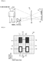
Fig. 3 illustrates an application example of the infrared detection device according to the present invention. -
Fig. 4 is a plan view illustrating a constitution of an infrared detection element according to a second embodiment of the present invention. -
Fig. 5 is a plan view illustrating a constitution of an infrared detection element according to a third embodiment of the present invention. -
Fig. 6 is a side sectional view illustrating a constitution of an infrared detection element according to a fourth embodiment of the present invention. -
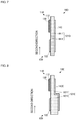
Fig. 7 is a side sectional view illustrating a constitution of an infrared detection element according to a fifth embodiment of the present invention. -
Fig. 8 is a side sectional view illustrating a constitution of an infrared detection element according to a sixth embodiment of the present invention. -
Fig. 9 is a circuit diagram of an infrared detection device in another form according to an embodiment of the present invention. - An infrared detection element and an infrared detection device according to a first embodiment of the present invention will be described below with reference to the drawings.
Fig. 1(A) is a plan view of the infrared detection element according to the first embodiment of the present invention.Fig. 1(B) is a sectional view taken along A-A inFig. 1(A) . - As illustrated in
Fig. 1 , theinfrared detection element 10 includes apyroelectric body 101, alight receiving electrode 110, a light receivingelectrode 120, a blackenedfilm 131, a blackenedfilm 132, andconnection electrodes light receiving electrode 110 corresponds to a "first light receiving electrode" in the present invention, and thelight receiving electrode 120 corresponds to a "second light receiving electrode" in the present invention. The blackenedfilm 131 corresponds to a "first blackened film" in the present invention, and the blackenedfilm 132 corresponds to a "second blackened film" in the present invention. - The
pyroelectric body 101 is made of a material generating the pyroelectric effect. Thepyroelectric body 101 is made of, for example, a ferroelectric material. Thepyroelectric body 101 is in the form of a flat plate. - The
light receiving electrode 110 and thelight receiving electrode 120 are formed on a front surface of thepyroelectric body 101. - The
light receiving electrode 110 includesdetection electrodes wiring electrode 113. Thedetection electrodes detection electrodes wiring electrode 113 is a linear electrode extending along the first direction. Thewiring electrode 113 interconnects thedetection electrode 111 and thedetection electrode 112. A length of thewiring electrode 113 along a second direction is shorter than that of thedetection electrode 111 along the second direction and that of thedetection electrode 112 along the second direction. Thus, thelight receiving electrode 110 is an H-shaped electrode when viewed in plan. Thedetection electrode 111 and thedetection electrode 112 preferably have the same shape. With thedetection electrode 111 and thedetection electrode 112 having the same shape, infrared detection accuracy is improved because both the detection electrodes are balanced to each other and stabilized with respect to variations of outside air temperature. - The
light receiving electrode 120 includesdetection electrodes wiring electrode 123. Thedetection electrodes detection electrodes wiring electrode 123 is a linear electrode extending along the first direction. Thewiring electrode 123 interconnects thedetection electrode 121 and thedetection electrode 122. A length of thewiring electrode 123 along the second direction is shorter than that of thedetection electrode 121 along the second direction and that of thedetection electrode 122 along the second direction. Thus, thelight receiving electrode 120 is an H-shaped electrode when viewed in plan. Thedetection electrode 121 and thedetection electrode 122 preferably have the same shape. With thedetection electrode 121 and thedetection electrode 122 having the same shape, infrared detection accuracy is improved. - The
light receiving electrode 110 and thelight receiving electrode 120 are arranged side by side in the second direction. Thelight receiving electrode 110 and thelight receiving electrode 120 are spaced from each other. - The blackened
film 131 is arranged over an entire surface of thedetection electrode 111 in thelight receiving electrode 110. The blackenedfilm 132 is arranged over an entire surface of thedetection electrode 112 in thelight receiving electrode 110. In other words, the blackenedfilms detection electrodes light receiving electrode 110. The blackenedfilms - With the above-described constitution, infrared reception sensitivity of the
light receiving electrode 110 becomes higher than that of thelight receiving electrode 120. Each of the blackenedfilms - Thus, detection sensitivity for infrared light detected by the
light receiving electrode 110 becomes higher than that for infrared light detected by thelight receiving electrode 120. Accordingly, infrared detection sensitivity in a first infrared-detection target region (corresponding to a "first region" in the present invention) assigned to thelight receiving electrode 110 is different from that in a second infrared-detection target region (corresponding to a "first region" in the present invention) assigned to thelight receiving electrode 120. Theinfrared detection element 10 constituted as described above enables detection of infrared light to be performed for plural regions providing different detection sensitivities with a simple constitution. As a result, a size of theinfrared detection element 10 can be reduced. - The
connection electrodes pyroelectric body 101. Theconnection electrode 141 is opposed to thedetection electrode 111 in thelight receiving electrode 110 and thedetection electrode 121 in thelight receiving electrode 120 with thepyroelectric body 101 interposed therebetween. Theconnection electrode 142 is opposed to thedetection electrode 112 in thelight receiving electrode 110 and thedetection electrode 122 in thelight receiving electrode 120 with thepyroelectric body 101 interposed therebetween. - The
infrared detection element 10 constituted as described above is used in an infrared detection device illustrated inFig. 2. Fig. 2 is a circuit diagram of the infrared detection device according to the first embodiment of the present invention. - As illustrated in
Fig. 2 , theinfrared detection device 30 includes aninfrared detection element 10, animpedance conversion element 21, and adetermination unit 31. Theinfrared detection element 10 and theimpedance conversion element 21 constitute aninfrared sensor 20. Theinfrared sensor 20 has a ground terminal PG, a drive-voltage input terminal PD, and an output terminal PO. - The
infrared detection element 10 has the above-described constitution illustrated inFig. 1 . Theinfrared detection element 10 includes a first element E1 including thelight receiving electrode 110 and thepyroelectric body 101, and a second element E2 including thelight receiving electrode 120 and thepyroelectric body 101. The first element E1 and the second element E2 are connected in parallel by theconnection electrode 141 and theconnection electrode 142. - The
infrared detection element 10 is connected to theimpedance conversion element 21 through theconnection electrode 141. Theconnection electrode 141 corresponds to a "connection portion" in the present invention. Theinfrared detection element 10 is connected to the ground terminal PG through theconnection electrode 142. The ground terminal PG is grounded. - The
impedance conversion element 21 is constituted by an n-type FET, for example. A gate G of the n-type FET is connected to theconnection electrode 141. A drain of the n-type FET is connected to the drive-voltage input terminal PD. A source of the n-type FET is connected to the output terminal PO. - The
determination unit 31 is constituted by a microcomputer, etc. Thedetermination unit 31 is connected to the output terminal PO of theinfrared sensor 20. - When the
infrared detection element 10 detects infrared light, a voltage depending on generated electric charges is applied to the gate of the n-type FET constituting theimpedance conversion element 21. A drive voltage VDD is applied to theimpedance conversion element 21 via the drive-voltage input terminal PD. Theimpedance conversion element 21 outputs a source voltage having a magnitude depending on the gate voltage. This source voltage signal corresponds to a "detection signal" in the present invention. - The
determination unit 31 executes detection of the infrared light on the basis of the magnitude of the source voltage signal. - In the
infrared detection element 10, infrared detection sensitivity is different between the first element E1 including thelight receiving electrode 110 and the second element E2 including thelight receiving electrode 120. Accordingly, electric charges generated in detecting the infrared light are different between the first infrared-detection target region, i.e., a detection target of the first element E1, and the second infrared-detection target region, i.e., a detection target of the second element E2. Hence the magnitude (amplitude) of the detection signal output from theimpedance conversion element 21 is also different therebetween. - By detecting the magnitude of the detection signal, the
determination unit 31 can easily determine in which one of the first infrared-detection target region and the second infrared-detection target region the infrared light has been detected. - Furthermore, the
determination unit 31 previously stores a threshold for the magnitude of the detection signal, and compares the detection signal with the threshold. Depending on a comparison result, if the magnitude of the detection signal is not smaller than the threshold, thedetermination unit 31 determines that the infrared light has been detected. Thus, theinfrared detection device 30 can realize the detection of the infrared light in a manner of restricting (or exclusively aiming at) the detection target. -
Fig. 3 illustrates an application example of the infrared detection device according to the present invention. In the example ofFig. 3 , theinfrared detection device 30 includes an optical element OE. In the infrared detection device, the first infrared-detection target region TGR1 is set as a region targeting a human being, but not targeting a small animal, such as a dog, or a moving low-height heat source body. The second infrared-detection target region TGR2 is set to mainly target the small animal, such as the dog, or the moving low-height heat source body, and to allow part of the human being to be included therein. - With the above-described setting, in the
infrared detection element 10 and theinfrared detection device 30, the detection sensitivity can be increased for the region targeting the human being, but not targeting the small animal, and can be reduced for the region targeting the small animal. Accordingly, theinfrared detection element 10 and theinfrared detection device 30, each reliably detecting the human being and reliably not detecting the small animal, can be realized. Moreover, theinfrared detection device 30 is not required to include the detection circuit for each element, i.e., for each detection-target region. As a result, theinfrared detection device 30 can be realized in a small size with a simple constitution. - An infrared detection element according to a second embodiment of the present invention will be described below with reference to the drawing.
Fig. 4 is a plan view illustrating a constitution of the infrared detection element according to the second embodiment of the present invention. - As illustrated in
Fig. 4 , theinfrared detection element 10A according to the second embodiment is different from theinfrared detection element 10 according to the first embodiment in adding blackenedfilms infrared detection element 10A are similar to those of theinfrared detection element 10, and description of the same constituent elements is omitted. - The
infrared detection element 10A includes the blackenedfilms films film 151 is formed on a surface of thedetection electrode 121 in thelight receiving electrode 120. The blackenedfilm 151 covers part of thedetection electrode 121. More specifically, the blackenedfilm 151 is formed along sides of thedetection electrode 121. The blackenedfilm 151 is not formed in a central region of thedetection electrode 121. The blackenedfilm 152 is formed on a surface of thedetection electrode 122 in thelight receiving electrode 120. The blackenedfilm 152 covers part of thedetection electrode 122. More specifically, the blackenedfilm 152 is formed along sides of thedetection electrode 122. The blackenedfilm 152 is not formed in a central region of thedetection electrode 122. - With the above-described constitution, a coverage of the blackened
films light receiving electrode 110 can be made different from that of the blackenedfilms light receiving electrode 120. Accordingly, the light sensitivity of thelight receiving electrode 110 can be made different from that of thelight receiving electrode 120. Furthermore, with the above-described constitution, the sensitivity difference between the light sensitivity of thelight receiving electrode 110 and the light sensitivity of thelight receiving electrode 120 can be adjusted by adjusting the coverage of the blackenedfilms light receiving electrode 120. - An infrared detection element according to a third embodiment of the present invention will be described below with reference to the drawing.
Fig. 5 is a plan view illustrating a constitution of the infrared detection element according to the third embodiment of the present invention. - As illustrated in
Fig. 5 , theinfrared detection element 10B according to the third embodiment is different from theinfrared detection element 10 according to the first embodiment in adding blackenedfilms infrared detection element 10B are similar to those of theinfrared detection element 10, and description of the same constituent elements is omitted. - The
infrared detection element 10B includes the blackenedfilms films film 151B is formed over the entire surface of thedetection electrode 121 in thelight receiving electrode 120. The blackenedfilm 152B is formed over the entire surface of thedetection electrode 122 in thelight receiving electrode 120. - An infrared absorbance of the blackened
films films - Also with the above-described constitution, the light sensitivity of the
light receiving electrode 110 can be made different from that of thelight receiving electrode 120. Furthermore, with the above-described constitution, the difference between the light sensitivity of thelight receiving electrode 110 and the light sensitivity of thelight receiving electrode 120 can be adjusted by adjusting the difference between the infrared absorbance of the blackenedfilms films - An infrared detection element according to a fourth embodiment of the present invention will be described below with reference to the drawing.
Fig. 6 is a side sectional view illustrating a constitution of the infrared detection element according to the fourth embodiment of the present invention. - As illustrated in
Fig. 6 , theinfrared detection element 10C according to the fourth embodiment is different from theinfrared detection element 10 according to the first embodiment in including alight receiving electrode 120C instead of thelight receiving electrode 120. Other constituent elements of theinfrared detection element 10C are similar to those of theinfrared detection element 10, and description of the same constituent elements is omitted. - The
infrared detection element 10C includes thelight receiving electrode 120C. Thelight receiving electrode 120C has the same shape as thelight receiving electrode 120 in the first embodiment. An infrared absorbance of thelight receiving electrode 120C (i.e., the electrode including thedetection electrode 122C inFig. 6 ) is lower than that of the light receiving electrode 110 (i.e., the electrode including thedetection electrode 112 inFig. 6 ). - Also with the above-described constitution, the light sensitivity of the
light receiving electrode 110 can be made different from that of thelight receiving electrode 120C. Furthermore, with the above-described constitution of theinfrared detection element 10C, the difference in infrared detection sensitivity between the first element E1 and the second element E2 can be further increased due to the synergetic effect of both the difference in light sensitivity between thelight receiving electrode 110 and thelight receiving electrode 120, which is caused by the presence of the blackenedfilms light receiving electrode 110 and thelight receiving electrode 120C, which is caused by materials of those electrodes. - Moreover, with the above-described constitution, the sensitivity difference between the light sensitivity of the
light receiving electrode 110 and the light sensitivity of thelight receiving electrode 120C can be adjusted by adjusting the difference between the infrared absorbance of thelight receiving electrode 110 and the infrared absorbance of thelight receiving electrode 120C. - An infrared detection element according to a fifth embodiment of the present invention will be described below with reference to the drawing.
Fig. 7 is a side sectional view illustrating a constitution of the infrared detection element according to the fifth embodiment of the present invention. - As illustrated in
Fig. 7 , theinfrared detection element 10D according to the fifth embodiment is different from theinfrared detection element 10 according to the first embodiment in constitution of apyroelectric body 101D. Other constituent elements of theinfrared detection element 10D are similar to those of theinfrared detection element 10 according to the first embodiment, and description of the same constituent elements is omitted. - The
infrared detection element 10D includes thepyroelectric body 101D. Thepyroelectric body 101D includes afirst region 1011 and asecond region 1012. Thefirst region 1011 and thesecond region 1012 are arrayed side by side in the second direction. A polarizability of thefirst region 1011 is higher than that of thesecond region 1012. Thelight receiving electrode 110 is formed on a surface of thefirst region 1011. Thelight receiving electrode 120 is formed on a surface of thesecond region 1012. - With the above-described constitution, the difference in infrared detection sensitivity between the first element E1 and the second element E2 can be increased. Moreover, with the constitution of the
infrared detection element 10D, the difference in infrared detection sensitivity between the first element E1 and the second element E2 can be further increased due to the synergetic effect of both the difference in light sensitivity between thelight receiving electrode 110 and thelight receiving electrode 120, which is caused by the presence of the blackenedfilms first region 1011 and thesecond region 1012 of thepyroelectric body 101D. - An infrared detection element according to a sixth embodiment of the present invention will be described below with reference to the drawing.
Fig. 8 is a side sectional view illustrating a constitution of the infrared detection element according to the sixth embodiment of the present invention. - As illustrated in
Fig. 8 , theinfrared detection element 10E according to the sixth embodiment is different from theinfrared detection element 10 according to the first embodiment in constitution of apyroelectric body 101E. Other constituent elements of theinfrared detection element 10E are similar to those of theinfrared detection element 10 according to the first embodiment, and description of the same constituent elements is omitted. - The
infrared detection element 10E includes thepyroelectric body 101E. Thepyroelectric body 101E includes afirst region 1011 and asecond region 1013. Thefirst region 1011 and thesecond region 1013 are arrayed side by side in the second direction. A thickness of thefirst region 1011 is smaller than that of thesecond region 1013. Thelight receiving electrode 110 is formed on a surface of thefirst region 1011. Thelight receiving electrode 120 is formed on a surface of thesecond region 1013. Because of having the above-described constitution, a capacitance formed in thefirst region 1011 between thelight receiving electrode 110 and each of theconnection electrodes second region 1013 between thelight receiving electrode 120 and each of theconnection electrodes - With the above-described constitution, the difference in infrared detection sensitivity between the first element E1 and the second element E2 can be increased. Moreover, with the constitution of the
infrared detection element 10E, the difference in infrared detection sensitivity between the first element E1 and the second element E2 can be further increased due to the synergetic effect of both the difference in light sensitivity between thelight receiving electrode 110 and thelight receiving electrode 120, which is caused by the presence of the blackenedfilms first region 1011 and thesecond region 1013 of thepyroelectric body 101D. - The constitutions of the above-described embodiments can be combined with each other as appropriate. Various advantageous effects can be obtained depending on the combinations of the constitutions.
- The first embodiment illustrates the constitution in which the first element E1 and the second element E2 are connected in parallel. However, the constitution may be modified as illustrated in
Fig. 9. Fig. 9 is a circuit diagram of an infrared detection device in another form according to an embodiment of the present invention. - As illustrated in
Fig. 9 , in aninfrared detection element 10F, the first element E1 and the second element E2 are connected in series. In aninfrared detection device 30F, the serial circuit is connected between theimpedance conversion element 21 and the ground terminal PG. - The above-described constitution can also provide similar advantageous to those obtained with the
infrared detection element 10 and theinfrared detection device 30, illustrated inFig. 2 , according to the first embodiment. - While the above description has been made in connection with the case in which the detection electrode has the rectangular shape, the detection electrode may have a polygonal or circular shape.
-
- 10, 10A, 10B, 10C, 10D, 10E, 10F: infrared detection element
- 20: infrared sensor
- 21: impedance conversion element
- 30, 30F: infrared detection device
- 31: determination unit
- 101, 101D, 101E: pyroelectric body
- 110: light receiving electrode
- 111, 112: detection electrode
- 113, 123: wiring electrode
- 120, 120C: light receiving electrode
- 121, 122, 122C: detection electrode
- 131, 132, 151, 151B, 152, 152B: blackened film
- 141, 142: connection electrode
- 1011: first region
- 1012, 1013: second region
- E1: first element
- E2: second element
- OE: Optical element
- PD: drive-voltage input terminal
- PG: ground terminal
- PO: output terminal
- TGR1: first infrared-detection target region
- TGR2: second infrared-detection target region
- VDD: drive voltage
Claims (8)
- An infrared detection element comprising:a pyroelectric body;a first light receiving electrode formed on a surface of the pyroelectric body and receiving infrared light from a first region;a second light receiving electrode formed on a surface of the pyroelectric body and receiving infrared light from a second region; anda light-sensitivity adjustment member making infrared reception sensitivity different between the first light receiving electrode and the second light receiving electrode.
- The infrared detection element according to Claim 1, wherein the light-sensitivity adjustment member is an infrared absorption film arranged only on a surface of the first light receiving electrode.
- The infrared detection element according to Claim 1, wherein the light-sensitivity adjustment member is given by a first infrared absorption film arranged on a surface of the first light receiving electrode, and a second infrared absorption film arranged on a surface of the second light receiving electrode, and
the first infrared absorption film has a higher infrared absorbance than the second infrared absorption film. - The infrared detection element according to Claim 3, wherein a coverage of the first infrared absorption film with respect to the surface of the first light receiving electrode is higher than a coverage of the second infrared absorption film with respect to the surface of the second light receiving electrode.
- The infrared detection element according to any one of Claims 1 to 4, wherein the first light receiving electrode has a higher infrared absorbance than the second light receiving electrode.
- The infrared detection element according to any one of Claims 1 to 5, wherein a polarizability of the pyroelectric body is different between a first region in which the first light receiving electrode is formed on the surface of the pyroelectric body and a second region in which the second light receiving electrode is formed on the surface of the pyroelectric body, and
the first region has a higher polarizability than the second region. - The infrared detection element according to any one of Claims 1 to 6, wherein a thickness of the pyroelectric body is different between a first region in which the first light receiving electrode is formed on the surface of the pyroelectric body and a second region in which the second light receiving electrode is formed on the surface of the pyroelectric body, and
the pyroelectric body in the first region has a smaller thickness than the pyroelectric body in the second region. - An infrared detection device including components of the infrared detection element according to any one of Claims 1 to 7, the infrared detection device comprising:a first element including the first light receiving electrode and the pyroelectric body;a second element including the second light receiving electrode and the pyroelectric body;a connection portion interconnecting the first element and the second element;an impedance conversion element generating detection signals from electric charges in the first element and the second element through the connection portion; anda determination unit determining detection of infrared light on basis of the detection signals.
Applications Claiming Priority (2)
| Application Number | Priority Date | Filing Date | Title |
|---|---|---|---|
| JP2016124260 | 2016-06-23 | ||
| PCT/JP2017/021251 WO2017221718A1 (en) | 2016-06-23 | 2017-06-08 | Infrared detection element and infrared detection device |
Publications (3)
| Publication Number | Publication Date |
|---|---|
| EP3477267A1 true EP3477267A1 (en) | 2019-05-01 |
| EP3477267A4 EP3477267A4 (en) | 2020-02-19 |
| EP3477267B1 EP3477267B1 (en) | 2024-11-06 |
Family
ID=60784216
Family Applications (1)
| Application Number | Title | Priority Date | Filing Date |
|---|---|---|---|
| EP17815187.4A Active EP3477267B1 (en) | 2016-06-23 | 2017-06-08 | Infrared detection element and infrared detection device |
Country Status (4)
| Country | Link |
|---|---|
| US (1) | US10823620B2 (en) |
| EP (1) | EP3477267B1 (en) |
| CN (1) | CN109328295B (en) |
| WO (1) | WO2017221718A1 (en) |
Families Citing this family (1)
| Publication number | Priority date | Publication date | Assignee | Title |
|---|---|---|---|---|
| CN112768598B (en) * | 2021-01-27 | 2022-11-15 | 山东大学 | A kind of infrared pyroelectric detector and preparation method thereof |
Family Cites Families (21)
| Publication number | Priority date | Publication date | Assignee | Title |
|---|---|---|---|---|
| EP0224595A4 (en) * | 1985-06-06 | 1989-10-24 | Nippon Ceramic Kk | Pyroelectric infrared sensor. |
| JPS62276422A (en) * | 1986-05-23 | 1987-12-01 | Nippon Ceramic Kk | Infrared sensor |
| CN1003103B (en) * | 1986-05-07 | 1989-01-18 | 日本陶瓷株式会社 | Pyroelectric Infrared Detector |
| US5528038A (en) | 1991-05-07 | 1996-06-18 | Matsushita Electric Industrial Co., Ltd. | Temperature distribution measurement apparatus and its application to a human body detecting system |
| JP3114235B2 (en) * | 1991-05-28 | 2000-12-04 | 松下電器産業株式会社 | Pyroelectric array sensor |
| JPH05164608A (en) * | 1991-12-17 | 1993-06-29 | Horiba Ltd | Pyroelectric infrared-ray detector |
| JPH08178748A (en) | 1994-12-26 | 1996-07-12 | Murata Mfg Co Ltd | Pyroelectric array sensor |
| JPH08184493A (en) * | 1994-12-27 | 1996-07-16 | Horiba Ltd | Pyroelectric multielement detector |
| JPH1062243A (en) * | 1996-08-19 | 1998-03-06 | Murata Mfg Co Ltd | Pyroelectric infrared sensor |
| JP2000292551A (en) | 1999-04-02 | 2000-10-20 | Nippon Ceramic Co Ltd | Pyroelectric infrared detector |
| CN102197290A (en) * | 2008-09-25 | 2011-09-21 | 松下电工株式会社 | Infrared sensor |
| DE102010013663A1 (en) * | 2010-04-01 | 2011-10-06 | Perkinelmer Technologies Gmbh & Co. Kg | radiation sensor |
| US8766187B2 (en) | 2010-10-25 | 2014-07-01 | Nec Tokin Corporation | Pyroelectric sensor array and pyroelectric infrared detection device |
| JP5226883B2 (en) * | 2011-02-01 | 2013-07-03 | Necトーキン株式会社 | Pyroelectric infrared sensor |
| JP5790001B2 (en) * | 2011-02-03 | 2015-10-07 | 日産自動車株式会社 | Infrared detector |
| JP5736906B2 (en) * | 2011-03-30 | 2015-06-17 | 三菱マテリアル株式会社 | Infrared sensor |
| WO2013084787A1 (en) * | 2011-12-05 | 2013-06-13 | 日本碍子株式会社 | Infrared detection element, infrared detection module, and method for manufacturing infrared detection module |
| JP2013195148A (en) * | 2012-03-16 | 2013-09-30 | Ricoh Co Ltd | Infrared sensor device |
| JP5966157B2 (en) * | 2012-06-18 | 2016-08-10 | パナソニックIpマネジメント株式会社 | Infrared detector |
| WO2014082097A1 (en) * | 2012-11-26 | 2014-05-30 | Flir Systems, Inc. | Hybrid infrared sensor array having heterogeneous infrared sensors |
| WO2014112392A1 (en) * | 2013-01-21 | 2014-07-24 | パナソニック株式会社 | Infrared detection element, infrared detector, and infrared type gas sensor |
-
2017
- 2017-06-08 WO PCT/JP2017/021251 patent/WO2017221718A1/en not_active Ceased
- 2017-06-08 EP EP17815187.4A patent/EP3477267B1/en active Active
- 2017-06-08 CN CN201780037247.2A patent/CN109328295B/en active Active
-
2018
- 2018-11-30 US US16/205,261 patent/US10823620B2/en active Active
Also Published As
| Publication number | Publication date |
|---|---|
| US20190101450A1 (en) | 2019-04-04 |
| CN109328295A (en) | 2019-02-12 |
| US10823620B2 (en) | 2020-11-03 |
| CN109328295B (en) | 2021-06-11 |
| EP3477267B1 (en) | 2024-11-06 |
| WO2017221718A1 (en) | 2017-12-28 |
| EP3477267A4 (en) | 2020-02-19 |
Similar Documents
| Publication | Publication Date | Title |
|---|---|---|
| EP3345014B1 (en) | Pixel receiver with capacitance cancellation for ultrasonic imaging apparatus | |
| CN109827907B (en) | Optical signal processing method and device | |
| US5567942A (en) | Infrared array sensor system | |
| US9222839B2 (en) | Detection circuit, sensor device and electronic apparatus | |
| US10436733B2 (en) | Method of measuring capacitance of row and column electrodes of capacitive imaging device | |
| KR0151302B1 (en) | Sensor and sensing method by using infrared rays for place judgement | |
| US20090309605A1 (en) | Electric potential sensor | |
| US8547170B1 (en) | Multimode integration circuit for sensor readout | |
| WO2008116699A3 (en) | Optical sensor chip and jamming protection device comprising such a chip | |
| WO2005022947A3 (en) | Parametric tranducer having an emitter film | |
| CN108572371B (en) | TOF camera, motor vehicle, method for manufacturing camera and method for determining distance | |
| EP3477267A1 (en) | Infrared detection element and infrared detection device | |
| US20040189149A1 (en) | Transconductance circuit for piezoelectric transducer | |
| US20200066715A1 (en) | Photon detector | |
| US8629726B1 (en) | High-performance amplifier for transducer array input unit cell | |
| CN102246417B (en) | Sensor device for detecting an object in a detection area | |
| US20050016283A1 (en) | Transconductance circuit for piezoelectric transducer | |
| US9151675B2 (en) | Dual-switching sensing device, and dual-function switching circuit thereof | |
| JP2013221906A (en) | Sensor device and electronic apparatus | |
| EP1452933A3 (en) | Sensor device and electronic watch | |
| PH12015000445B1 (en) | Radiation detection apparatus and radiation imaging system | |
| EP4288747A1 (en) | Distance measurement using field of view | |
| US20160178758A1 (en) | Radiation detection apparatus and radiation imaging system | |
| EP3268706B1 (en) | Differential circuit for pyroelectric infrared detector | |
| JP2011252869A (en) | Pyroelectric element and pyroelectric type infrared sensor |
Legal Events
| Date | Code | Title | Description |
|---|---|---|---|
| STAA | Information on the status of an ep patent application or granted ep patent |
Free format text: STATUS: THE INTERNATIONAL PUBLICATION HAS BEEN MADE |
|
| PUAI | Public reference made under article 153(3) epc to a published international application that has entered the european phase |
Free format text: ORIGINAL CODE: 0009012 |
|
| STAA | Information on the status of an ep patent application or granted ep patent |
Free format text: STATUS: REQUEST FOR EXAMINATION WAS MADE |
|
| 17P | Request for examination filed |
Effective date: 20181115 |
|
| AK | Designated contracting states |
Kind code of ref document: A1 Designated state(s): AL AT BE BG CH CY CZ DE DK EE ES FI FR GB GR HR HU IE IS IT LI LT LU LV MC MK MT NL NO PL PT RO RS SE SI SK SM TR |
|
| AX | Request for extension of the european patent |
Extension state: BA ME |
|
| DAV | Request for validation of the european patent (deleted) | ||
| DAX | Request for extension of the european patent (deleted) | ||
| A4 | Supplementary search report drawn up and despatched |
Effective date: 20200121 |
|
| RIC1 | Information provided on ipc code assigned before grant |
Ipc: G01J 5/34 20060101AFI20200115BHEP Ipc: H01L 37/02 20060101ALI20200115BHEP Ipc: G08B 13/191 20060101ALI20200115BHEP Ipc: G01J 5/02 20060101ALI20200115BHEP Ipc: G01J 5/00 20060101ALI20200115BHEP Ipc: G01J 5/08 20060101ALI20200115BHEP |
|
| STAA | Information on the status of an ep patent application or granted ep patent |
Free format text: STATUS: EXAMINATION IS IN PROGRESS |
|
| 17Q | First examination report despatched |
Effective date: 20221031 |
|
| REG | Reference to a national code |
Ref country code: DE Ref legal event code: R079 Free format text: PREVIOUS MAIN CLASS: G01J0001020000 Ipc: G01J0005340000 Ref country code: DE Ref legal event code: R079 Ref document number: 602017085967 Country of ref document: DE Free format text: PREVIOUS MAIN CLASS: G01J0001020000 Ipc: G01J0005340000 |
|
| GRAP | Despatch of communication of intention to grant a patent |
Free format text: ORIGINAL CODE: EPIDOSNIGR1 |
|
| STAA | Information on the status of an ep patent application or granted ep patent |
Free format text: STATUS: GRANT OF PATENT IS INTENDED |
|
| RIC1 | Information provided on ipc code assigned before grant |
Ipc: G01J 5/07 20220101ALI20240523BHEP Ipc: H10N 15/10 20230101ALI20240523BHEP Ipc: G01J 5/02 20060101ALI20240523BHEP Ipc: G01J 5/00 20060101ALI20240523BHEP Ipc: G01J 5/08 20060101ALI20240523BHEP Ipc: G08B 13/191 20060101ALI20240523BHEP Ipc: G01J 5/34 20060101AFI20240523BHEP |
|
| INTG | Intention to grant announced |
Effective date: 20240613 |
|
| RIN1 | Information on inventor provided before grant (corrected) |
Inventor name: OTAKE, TOMONORI |
|
| GRAS | Grant fee paid |
Free format text: ORIGINAL CODE: EPIDOSNIGR3 |
|
| GRAA | (expected) grant |
Free format text: ORIGINAL CODE: 0009210 |
|
| STAA | Information on the status of an ep patent application or granted ep patent |
Free format text: STATUS: THE PATENT HAS BEEN GRANTED |
|
| AK | Designated contracting states |
Kind code of ref document: B1 Designated state(s): AL AT BE BG CH CY CZ DE DK EE ES FI FR GB GR HR HU IE IS IT LI LT LU LV MC MK MT NL NO PL PT RO RS SE SI SK SM TR |
|
| REG | Reference to a national code |
Ref country code: GB Ref legal event code: FG4D |
|
| REG | Reference to a national code |
Ref country code: CH Ref legal event code: EP |
|
| REG | Reference to a national code |
Ref country code: DE Ref legal event code: R096 Ref document number: 602017085967 Country of ref document: DE |
|
| REG | Reference to a national code |
Ref country code: IE Ref legal event code: FG4D |
|
| REG | Reference to a national code |
Ref country code: LT Ref legal event code: MG9D |
|
| REG | Reference to a national code |
Ref country code: NL Ref legal event code: MP Effective date: 20241106 |
|
| PG25 | Lapsed in a contracting state [announced via postgrant information from national office to epo] |
Ref country code: IS Free format text: LAPSE BECAUSE OF FAILURE TO SUBMIT A TRANSLATION OF THE DESCRIPTION OR TO PAY THE FEE WITHIN THE PRESCRIBED TIME-LIMIT Effective date: 20250306 Ref country code: PT Free format text: LAPSE BECAUSE OF FAILURE TO SUBMIT A TRANSLATION OF THE DESCRIPTION OR TO PAY THE FEE WITHIN THE PRESCRIBED TIME-LIMIT Effective date: 20250306 Ref country code: HR Free format text: LAPSE BECAUSE OF FAILURE TO SUBMIT A TRANSLATION OF THE DESCRIPTION OR TO PAY THE FEE WITHIN THE PRESCRIBED TIME-LIMIT Effective date: 20241106 |
|
| PG25 | Lapsed in a contracting state [announced via postgrant information from national office to epo] |
Ref country code: FI Free format text: LAPSE BECAUSE OF FAILURE TO SUBMIT A TRANSLATION OF THE DESCRIPTION OR TO PAY THE FEE WITHIN THE PRESCRIBED TIME-LIMIT Effective date: 20241106 Ref country code: NL Free format text: LAPSE BECAUSE OF FAILURE TO SUBMIT A TRANSLATION OF THE DESCRIPTION OR TO PAY THE FEE WITHIN THE PRESCRIBED TIME-LIMIT Effective date: 20241106 |
|
| REG | Reference to a national code |
Ref country code: AT Ref legal event code: MK05 Ref document number: 1739811 Country of ref document: AT Kind code of ref document: T Effective date: 20241106 |
|
| PG25 | Lapsed in a contracting state [announced via postgrant information from national office to epo] |
Ref country code: BG Free format text: LAPSE BECAUSE OF FAILURE TO SUBMIT A TRANSLATION OF THE DESCRIPTION OR TO PAY THE FEE WITHIN THE PRESCRIBED TIME-LIMIT Effective date: 20241106 |
|
| PG25 | Lapsed in a contracting state [announced via postgrant information from national office to epo] |
Ref country code: ES Free format text: LAPSE BECAUSE OF FAILURE TO SUBMIT A TRANSLATION OF THE DESCRIPTION OR TO PAY THE FEE WITHIN THE PRESCRIBED TIME-LIMIT Effective date: 20241106 |
|
| PG25 | Lapsed in a contracting state [announced via postgrant information from national office to epo] |
Ref country code: NO Free format text: LAPSE BECAUSE OF FAILURE TO SUBMIT A TRANSLATION OF THE DESCRIPTION OR TO PAY THE FEE WITHIN THE PRESCRIBED TIME-LIMIT Effective date: 20250206 |
|
| PG25 | Lapsed in a contracting state [announced via postgrant information from national office to epo] |
Ref country code: AT Free format text: LAPSE BECAUSE OF FAILURE TO SUBMIT A TRANSLATION OF THE DESCRIPTION OR TO PAY THE FEE WITHIN THE PRESCRIBED TIME-LIMIT Effective date: 20241106 Ref country code: GR Free format text: LAPSE BECAUSE OF FAILURE TO SUBMIT A TRANSLATION OF THE DESCRIPTION OR TO PAY THE FEE WITHIN THE PRESCRIBED TIME-LIMIT Effective date: 20250207 Ref country code: LV Free format text: LAPSE BECAUSE OF FAILURE TO SUBMIT A TRANSLATION OF THE DESCRIPTION OR TO PAY THE FEE WITHIN THE PRESCRIBED TIME-LIMIT Effective date: 20241106 |
|
| PG25 | Lapsed in a contracting state [announced via postgrant information from national office to epo] |
Ref country code: PL Free format text: LAPSE BECAUSE OF FAILURE TO SUBMIT A TRANSLATION OF THE DESCRIPTION OR TO PAY THE FEE WITHIN THE PRESCRIBED TIME-LIMIT Effective date: 20241106 |
|
| PG25 | Lapsed in a contracting state [announced via postgrant information from national office to epo] |
Ref country code: RS Free format text: LAPSE BECAUSE OF FAILURE TO SUBMIT A TRANSLATION OF THE DESCRIPTION OR TO PAY THE FEE WITHIN THE PRESCRIBED TIME-LIMIT Effective date: 20250206 |
|
| PG25 | Lapsed in a contracting state [announced via postgrant information from national office to epo] |
Ref country code: SM Free format text: LAPSE BECAUSE OF FAILURE TO SUBMIT A TRANSLATION OF THE DESCRIPTION OR TO PAY THE FEE WITHIN THE PRESCRIBED TIME-LIMIT Effective date: 20241106 |
|
| PGFP | Annual fee paid to national office [announced via postgrant information from national office to epo] |
Ref country code: DE Payment date: 20250618 Year of fee payment: 9 |
|
| PG25 | Lapsed in a contracting state [announced via postgrant information from national office to epo] |
Ref country code: DK Free format text: LAPSE BECAUSE OF FAILURE TO SUBMIT A TRANSLATION OF THE DESCRIPTION OR TO PAY THE FEE WITHIN THE PRESCRIBED TIME-LIMIT Effective date: 20241106 |
|
| PG25 | Lapsed in a contracting state [announced via postgrant information from national office to epo] |
Ref country code: EE Free format text: LAPSE BECAUSE OF FAILURE TO SUBMIT A TRANSLATION OF THE DESCRIPTION OR TO PAY THE FEE WITHIN THE PRESCRIBED TIME-LIMIT Effective date: 20241106 |
|
| PG25 | Lapsed in a contracting state [announced via postgrant information from national office to epo] |
Ref country code: RO Free format text: LAPSE BECAUSE OF FAILURE TO SUBMIT A TRANSLATION OF THE DESCRIPTION OR TO PAY THE FEE WITHIN THE PRESCRIBED TIME-LIMIT Effective date: 20241106 |
|
| PG25 | Lapsed in a contracting state [announced via postgrant information from national office to epo] |
Ref country code: SK Free format text: LAPSE BECAUSE OF FAILURE TO SUBMIT A TRANSLATION OF THE DESCRIPTION OR TO PAY THE FEE WITHIN THE PRESCRIBED TIME-LIMIT Effective date: 20241106 |
|
| PG25 | Lapsed in a contracting state [announced via postgrant information from national office to epo] |
Ref country code: CZ Free format text: LAPSE BECAUSE OF FAILURE TO SUBMIT A TRANSLATION OF THE DESCRIPTION OR TO PAY THE FEE WITHIN THE PRESCRIBED TIME-LIMIT Effective date: 20241106 |
|
| PG25 | Lapsed in a contracting state [announced via postgrant information from national office to epo] |
Ref country code: IT Free format text: LAPSE BECAUSE OF FAILURE TO SUBMIT A TRANSLATION OF THE DESCRIPTION OR TO PAY THE FEE WITHIN THE PRESCRIBED TIME-LIMIT Effective date: 20241106 |
|
| REG | Reference to a national code |
Ref country code: DE Ref legal event code: R097 Ref document number: 602017085967 Country of ref document: DE |
|
| PG25 | Lapsed in a contracting state [announced via postgrant information from national office to epo] |
Ref country code: SE Free format text: LAPSE BECAUSE OF FAILURE TO SUBMIT A TRANSLATION OF THE DESCRIPTION OR TO PAY THE FEE WITHIN THE PRESCRIBED TIME-LIMIT Effective date: 20241106 |
|
| PLBE | No opposition filed within time limit |
Free format text: ORIGINAL CODE: 0009261 |
|
| STAA | Information on the status of an ep patent application or granted ep patent |
Free format text: STATUS: NO OPPOSITION FILED WITHIN TIME LIMIT |
|
| 26N | No opposition filed |
Effective date: 20250807 |
|
| REG | Reference to a national code |
Ref country code: CH Ref legal event code: H13 Free format text: ST27 STATUS EVENT CODE: U-0-0-H10-H13 (AS PROVIDED BY THE NATIONAL OFFICE) Effective date: 20260127 |
|
| PG25 | Lapsed in a contracting state [announced via postgrant information from national office to epo] |
Ref country code: MC Free format text: LAPSE BECAUSE OF FAILURE TO SUBMIT A TRANSLATION OF THE DESCRIPTION OR TO PAY THE FEE WITHIN THE PRESCRIBED TIME-LIMIT Effective date: 20241106 |
|
| PG25 | Lapsed in a contracting state [announced via postgrant information from national office to epo] |
Ref country code: LU Free format text: LAPSE BECAUSE OF NON-PAYMENT OF DUE FEES Effective date: 20250608 |
|
| GBPC | Gb: european patent ceased through non-payment of renewal fee |
Effective date: 20250608 |
|
| REG | Reference to a national code |
Ref country code: BE Ref legal event code: MM Effective date: 20250630 |
|
| PG25 | Lapsed in a contracting state [announced via postgrant information from national office to epo] |
Ref country code: GB Free format text: LAPSE BECAUSE OF NON-PAYMENT OF DUE FEES Effective date: 20250608 |
|
| PG25 | Lapsed in a contracting state [announced via postgrant information from national office to epo] |
Ref country code: IE Free format text: LAPSE BECAUSE OF NON-PAYMENT OF DUE FEES Effective date: 20250608 |
|
| PG25 | Lapsed in a contracting state [announced via postgrant information from national office to epo] |
Ref country code: BE Free format text: LAPSE BECAUSE OF NON-PAYMENT OF DUE FEES Effective date: 20250630 |
|
| PG25 | Lapsed in a contracting state [announced via postgrant information from national office to epo] |
Ref country code: FR Free format text: LAPSE BECAUSE OF NON-PAYMENT OF DUE FEES Effective date: 20250630 |
|
| PG25 | Lapsed in a contracting state [announced via postgrant information from national office to epo] |
Ref country code: CH Free format text: LAPSE BECAUSE OF NON-PAYMENT OF DUE FEES Effective date: 20250630 |