EP3475999B1 - A method of manufacturing a lithium battery - Google Patents
A method of manufacturing a lithium battery Download PDFInfo
- Publication number
- EP3475999B1 EP3475999B1 EP17737899.9A EP17737899A EP3475999B1 EP 3475999 B1 EP3475999 B1 EP 3475999B1 EP 17737899 A EP17737899 A EP 17737899A EP 3475999 B1 EP3475999 B1 EP 3475999B1
- Authority
- EP
- European Patent Office
- Prior art keywords
- layer
- electrode
- lithium
- current collector
- conductive
- Prior art date
- Legal status (The legal status is an assumption and is not a legal conclusion. Google has not performed a legal analysis and makes no representation as to the accuracy of the status listed.)
- Active
Links
Images


Classifications
-
- H—ELECTRICITY
- H01—ELECTRIC ELEMENTS
- H01M—PROCESSES OR MEANS, e.g. BATTERIES, FOR THE DIRECT CONVERSION OF CHEMICAL ENERGY INTO ELECTRICAL ENERGY
- H01M4/00—Electrodes
- H01M4/02—Electrodes composed of, or comprising, active material
- H01M4/04—Processes of manufacture in general
- H01M4/0438—Processes of manufacture in general by electrochemical processing
- H01M4/045—Electrochemical coating; Electrochemical impregnation
- H01M4/0452—Electrochemical coating; Electrochemical impregnation from solutions
-
- H—ELECTRICITY
- H01—ELECTRIC ELEMENTS
- H01M—PROCESSES OR MEANS, e.g. BATTERIES, FOR THE DIRECT CONVERSION OF CHEMICAL ENERGY INTO ELECTRICAL ENERGY
- H01M10/00—Secondary cells; Manufacture thereof
- H01M10/05—Accumulators with non-aqueous electrolyte
- H01M10/058—Construction or manufacture
-
- H—ELECTRICITY
- H01—ELECTRIC ELEMENTS
- H01M—PROCESSES OR MEANS, e.g. BATTERIES, FOR THE DIRECT CONVERSION OF CHEMICAL ENERGY INTO ELECTRICAL ENERGY
- H01M10/00—Secondary cells; Manufacture thereof
- H01M10/04—Construction or manufacture in general
- H01M10/0413—Large-sized flat cells or batteries for motive or stationary systems with plate-like electrodes
-
- H—ELECTRICITY
- H01—ELECTRIC ELEMENTS
- H01M—PROCESSES OR MEANS, e.g. BATTERIES, FOR THE DIRECT CONVERSION OF CHEMICAL ENERGY INTO ELECTRICAL ENERGY
- H01M10/00—Secondary cells; Manufacture thereof
- H01M10/04—Construction or manufacture in general
- H01M10/0436—Small-sized flat cells or batteries for portable equipment
-
- H—ELECTRICITY
- H01—ELECTRIC ELEMENTS
- H01M—PROCESSES OR MEANS, e.g. BATTERIES, FOR THE DIRECT CONVERSION OF CHEMICAL ENERGY INTO ELECTRICAL ENERGY
- H01M10/00—Secondary cells; Manufacture thereof
- H01M10/05—Accumulators with non-aqueous electrolyte
- H01M10/052—Li-accumulators
-
- H—ELECTRICITY
- H01—ELECTRIC ELEMENTS
- H01M—PROCESSES OR MEANS, e.g. BATTERIES, FOR THE DIRECT CONVERSION OF CHEMICAL ENERGY INTO ELECTRICAL ENERGY
- H01M10/00—Secondary cells; Manufacture thereof
- H01M10/05—Accumulators with non-aqueous electrolyte
- H01M10/052—Li-accumulators
- H01M10/0525—Rocking-chair batteries, i.e. batteries with lithium insertion or intercalation in both electrodes; Lithium-ion batteries
-
- H—ELECTRICITY
- H01—ELECTRIC ELEMENTS
- H01M—PROCESSES OR MEANS, e.g. BATTERIES, FOR THE DIRECT CONVERSION OF CHEMICAL ENERGY INTO ELECTRICAL ENERGY
- H01M10/00—Secondary cells; Manufacture thereof
- H01M10/05—Accumulators with non-aqueous electrolyte
- H01M10/056—Accumulators with non-aqueous electrolyte characterised by the materials used as electrolytes, e.g. mixed inorganic/organic electrolytes
- H01M10/0561—Accumulators with non-aqueous electrolyte characterised by the materials used as electrolytes, e.g. mixed inorganic/organic electrolytes the electrolyte being constituted of inorganic materials only
- H01M10/0562—Solid materials
-
- H—ELECTRICITY
- H01—ELECTRIC ELEMENTS
- H01M—PROCESSES OR MEANS, e.g. BATTERIES, FOR THE DIRECT CONVERSION OF CHEMICAL ENERGY INTO ELECTRICAL ENERGY
- H01M10/00—Secondary cells; Manufacture thereof
- H01M10/05—Accumulators with non-aqueous electrolyte
- H01M10/058—Construction or manufacture
- H01M10/0585—Construction or manufacture of accumulators having only flat construction elements, i.e. flat positive electrodes, flat negative electrodes and flat separators
-
- H—ELECTRICITY
- H01—ELECTRIC ELEMENTS
- H01M—PROCESSES OR MEANS, e.g. BATTERIES, FOR THE DIRECT CONVERSION OF CHEMICAL ENERGY INTO ELECTRICAL ENERGY
- H01M4/00—Electrodes
- H01M4/02—Electrodes composed of, or comprising, active material
- H01M4/04—Processes of manufacture in general
- H01M4/0438—Processes of manufacture in general by electrochemical processing
- H01M4/045—Electrochemical coating; Electrochemical impregnation
-
- H—ELECTRICITY
- H01—ELECTRIC ELEMENTS
- H01M—PROCESSES OR MEANS, e.g. BATTERIES, FOR THE DIRECT CONVERSION OF CHEMICAL ENERGY INTO ELECTRICAL ENERGY
- H01M4/00—Electrodes
- H01M4/02—Electrodes composed of, or comprising, active material
- H01M4/13—Electrodes for accumulators with non-aqueous electrolyte, e.g. for lithium-accumulators; Processes of manufacture thereof
- H01M4/134—Electrodes based on metals, Si or alloys
-
- H—ELECTRICITY
- H01—ELECTRIC ELEMENTS
- H01M—PROCESSES OR MEANS, e.g. BATTERIES, FOR THE DIRECT CONVERSION OF CHEMICAL ENERGY INTO ELECTRICAL ENERGY
- H01M4/00—Electrodes
- H01M4/02—Electrodes composed of, or comprising, active material
- H01M4/13—Electrodes for accumulators with non-aqueous electrolyte, e.g. for lithium-accumulators; Processes of manufacture thereof
- H01M4/139—Processes of manufacture
- H01M4/1395—Processes of manufacture of electrodes based on metals, Si or alloys
-
- H—ELECTRICITY
- H01—ELECTRIC ELEMENTS
- H01M—PROCESSES OR MEANS, e.g. BATTERIES, FOR THE DIRECT CONVERSION OF CHEMICAL ENERGY INTO ELECTRICAL ENERGY
- H01M4/00—Electrodes
- H01M4/02—Electrodes composed of, or comprising, active material
- H01M4/36—Selection of substances as active materials, active masses, active liquids
- H01M4/362—Composites
- H01M4/366—Composites as layered products
-
- H—ELECTRICITY
- H01—ELECTRIC ELEMENTS
- H01M—PROCESSES OR MEANS, e.g. BATTERIES, FOR THE DIRECT CONVERSION OF CHEMICAL ENERGY INTO ELECTRICAL ENERGY
- H01M4/00—Electrodes
- H01M4/02—Electrodes composed of, or comprising, active material
- H01M4/36—Selection of substances as active materials, active masses, active liquids
- H01M4/38—Selection of substances as active materials, active masses, active liquids of elements or alloys
- H01M4/381—Alkaline or alkaline earth metals elements
- H01M4/382—Lithium
-
- H—ELECTRICITY
- H01—ELECTRIC ELEMENTS
- H01M—PROCESSES OR MEANS, e.g. BATTERIES, FOR THE DIRECT CONVERSION OF CHEMICAL ENERGY INTO ELECTRICAL ENERGY
- H01M4/00—Electrodes
- H01M4/02—Electrodes composed of, or comprising, active material
- H01M4/64—Carriers or collectors
- H01M4/66—Selection of materials
- H01M4/661—Metal or alloys, e.g. alloy coatings
-
- H—ELECTRICITY
- H01—ELECTRIC ELEMENTS
- H01M—PROCESSES OR MEANS, e.g. BATTERIES, FOR THE DIRECT CONVERSION OF CHEMICAL ENERGY INTO ELECTRICAL ENERGY
- H01M4/00—Electrodes
- H01M4/02—Electrodes composed of, or comprising, active material
- H01M4/64—Carriers or collectors
- H01M4/70—Carriers or collectors characterised by shape or form
-
- H—ELECTRICITY
- H01—ELECTRIC ELEMENTS
- H01M—PROCESSES OR MEANS, e.g. BATTERIES, FOR THE DIRECT CONVERSION OF CHEMICAL ENERGY INTO ELECTRICAL ENERGY
- H01M4/00—Electrodes
- H01M4/02—Electrodes composed of, or comprising, active material
- H01M4/64—Carriers or collectors
- H01M4/70—Carriers or collectors characterised by shape or form
- H01M4/75—Wires, rods or strips
-
- H—ELECTRICITY
- H01—ELECTRIC ELEMENTS
- H01M—PROCESSES OR MEANS, e.g. BATTERIES, FOR THE DIRECT CONVERSION OF CHEMICAL ENERGY INTO ELECTRICAL ENERGY
- H01M2220/00—Batteries for particular applications
- H01M2220/20—Batteries in motive systems, e.g. vehicle, ship, plane
-
- Y—GENERAL TAGGING OF NEW TECHNOLOGICAL DEVELOPMENTS; GENERAL TAGGING OF CROSS-SECTIONAL TECHNOLOGIES SPANNING OVER SEVERAL SECTIONS OF THE IPC; TECHNICAL SUBJECTS COVERED BY FORMER USPC CROSS-REFERENCE ART COLLECTIONS [XRACs] AND DIGESTS
- Y02—TECHNOLOGIES OR APPLICATIONS FOR MITIGATION OR ADAPTATION AGAINST CLIMATE CHANGE
- Y02E—REDUCTION OF GREENHOUSE GAS [GHG] EMISSIONS, RELATED TO ENERGY GENERATION, TRANSMISSION OR DISTRIBUTION
- Y02E60/00—Enabling technologies; Technologies with a potential or indirect contribution to GHG emissions mitigation
- Y02E60/10—Energy storage using batteries
-
- Y—GENERAL TAGGING OF NEW TECHNOLOGICAL DEVELOPMENTS; GENERAL TAGGING OF CROSS-SECTIONAL TECHNOLOGIES SPANNING OVER SEVERAL SECTIONS OF THE IPC; TECHNICAL SUBJECTS COVERED BY FORMER USPC CROSS-REFERENCE ART COLLECTIONS [XRACs] AND DIGESTS
- Y02—TECHNOLOGIES OR APPLICATIONS FOR MITIGATION OR ADAPTATION AGAINST CLIMATE CHANGE
- Y02P—CLIMATE CHANGE MITIGATION TECHNOLOGIES IN THE PRODUCTION OR PROCESSING OF GOODS
- Y02P70/00—Climate change mitigation technologies in the production process for final industrial or consumer products
- Y02P70/50—Manufacturing or production processes characterised by the final manufactured product
-
- Y—GENERAL TAGGING OF NEW TECHNOLOGICAL DEVELOPMENTS; GENERAL TAGGING OF CROSS-SECTIONAL TECHNOLOGIES SPANNING OVER SEVERAL SECTIONS OF THE IPC; TECHNICAL SUBJECTS COVERED BY FORMER USPC CROSS-REFERENCE ART COLLECTIONS [XRACs] AND DIGESTS
- Y02—TECHNOLOGIES OR APPLICATIONS FOR MITIGATION OR ADAPTATION AGAINST CLIMATE CHANGE
- Y02T—CLIMATE CHANGE MITIGATION TECHNOLOGIES RELATED TO TRANSPORTATION
- Y02T10/00—Road transport of goods or passengers
- Y02T10/60—Other road transportation technologies with climate change mitigation effect
- Y02T10/70—Energy storage systems for electromobility, e.g. batteries
Definitions
- the present invention relates to a method of manufacturing a Lithium battery for electrochemical or electro-optical devices.
- lithium metal based batteries i.e. with lithium metal as anode
- US6168884 discloses a planar design of a lithium metal anode that is formed in-situ during initial charge by plating lithium on an anode current collector, which does not form inter-metallic compounds with lithium.
- the anode current collector is sandwiched between a solid state electrolyte and an overlying layer.
- DE102011121681 discloses a pillar geometry for a liquid electrolyte, wherein dendrites are prevented from forming on the pillar tops by isolating these.
- the pillars are extending in an electrolyte fluid or gel and distanced from a cathode sheet.
- WO2015126248 discloses a method of manufacturing a battery with a substrate current collector, wherein the method comprises: forming elongate and aligned electrically conductive structures on the substrate face with upstanding walls; wherein the walls are formed with a first electrode layer covering said walls, and a solid state electrolyte layer provided on the first electrode layer; and wherein a second electrode is formed by covering the electrolyte layer; and forming a top current collector layer in electrical contact with the second electrode.
- the anode In discharging battery mode, the anode is the "negative electrode” to which the positive current flows, from the cathode, being the “positive electrode”. During charge these functions are reversed.
- the electrochemical relationship may be characterized by charge exchange between a negative electrode material and a positive electrode material, the negative electrode material having a workfunction or redox potential that is lower than the workfunction or redox potential of the positive electrode material.
- known negative electrode (anode) materials are Li4Ti5O12 (LTO); LiC6 (Graphite); Li4.4 Si (Silicon) and Li4.4Ge (Germanium) known positive electrode (cathode) materials are LiCOO2 (LCO), LiCoPO4, (doped) LiMn2O4 (LMO), LiMnPO4, LiFePO4 (LFP), LiFePO4F(LFPF), LiCO1/3Ni1/3Mn1/3O2 (LCNMO), Sulphur or Sulphur based compounds like Li x S.
- Solid state electrolytes might include Garnets such as Li7La3Zr2O12 (LLZO), Perovskites such as La0.57Li0.33TiO3 (LLTO), lithium iodide (LiI), lithium phosphate (Li3PO4) and lithium phosphorus oxynitride (LiPON).
- LiPF6, LiBF4 or LiClO4 in an organic solvent such as ethylene carbonate, dimethyl carbonate, diethyl carbonate, propylene carbonate are known to have a typical conductivity of about 10 mS/cm at RT.
- the electrolyte decomposes on initial charging and forms a solid layer called the solid electrolyte interphase (SEI).
- SEI solid electrolyte interphase
- Solid polymer separators like polyethylene oxide (PEO) may also be included, such polymers having transport capacity often due to having a lithium salt disposed therein as known in the state of the art.
- Work has also been performed with lithium and halide materials, particularly, in some examples, a lithium aluminum tetrahalide such as lithium aluminum tetrafluoride (LiAlF4).
- LiAlF4 lithium aluminum tetrafluoride
- Such structures are made on a bendable metal foil, they can be manufactured in large-scale processes, e.g. a roll-to-roll process where the following can be done: 1) Coiling, winding or stacking it to increase the energy or power density per unit volume. 2) Integrating it on flexible devices like flexible displays, signage etc.
- high-aspect ratio structures can be made in nanometer scale the height or depth of these high-aspect ratio structures need to be in the microns range for delivering enough charge capacity for the battery.
- the reason why these structures are preferred is due to the easy accessibility of their entire surface.
- many methods to produce these are non-economical (e.g. involving silicon microfabrication and long-time electrodeposition).
- the design of the stack is in need for optimization because otherwise while winding or flexing, the pillar structure could be damaged inhibiting proper electrochemical action of the device.
- existing solid state (e.g.) Li-based intercalation electrolytes induce stress in the high-aspect ratio structures that may limit lifetime and reduce the number of cycle periods.
- a method is provided of manufacturing a battery according to claim 1.
- the pillars function as current collectors for the battery structure in a laminate, which current collectors are electrically connected through a base substrate.
- an aspect ratio of a height dimension and the pillar interdistance i.e. a length dimension normal to the walls coplanar along the base, is relatively high, that is, higher than 50, or even higher than 80 or even more than 100.
- the pillars may have height dimensions, i.e. a height separating a base plane from a planar surface of about 25-200 micrometer, preferably 50-100 micrometer wherein the length dimensions, i.e. the length separating opposing pillars, can be in the order of 1-10 micrometer, preferably 2-4 micrometer.
- the substrate as presently disclosed is electrically conductive with a surface area of the current collector that is significantly increased, which enhances the charge collecting capacity of the current collector.
- a conformal multilayer coating without compromising the functionality of the multilayer coating. Examples of such functionality may be multilayers such as a battery multilayer or photovoltaic multilayer or single layer coatings.
- optimal current collecting performance may be provided in the form of a coated pillar wherein the high-aspect ratio structure comprises metal or metalized pillars having a radius of curvature larger than 50 nanometer.
- An aspect of improved performance is a trade-off that is found by a density of the high-aspect ratio structure demanding smaller pitches and the surrounding conformal coating.
- electrode thicknesses in the battery multilayer may be varied and are correlated to match their volumetric storage capacities for Lithium-ions while charging and/or discharging.
- a known matching relationship is governed by a C-rate number, known in the art.
- a C-rate is a measure of the rate at which a battery is charged or discharged relative to its maximum capacity. For example the capacity of the electrode layers at a certain C-rate are matched by controlling layer thickness and material composition.
- a 'conformal coating' is a coating that may comprise a plurality of layers that at least conformally coat the pillars of the high aspect ratio structure.
- a 'first electrode layer' may be part of a laminate and may be a bottom layer, i.e. the layer with the smallest radius of curvature.
- the 'second electrode' may be used to indicate a top layer of a laminate, i.e. the layer with the highest radius of curvature.
- a laminate is not essential, since the electrode structures may be merged into the collector structures as porous complex structures. In such embodiments, an electrolyte layer is provided between electrode structures that are combined with current collector structures.
- thickness is meant 'average thickness' which may render an equivalent function of a certain mathematical thickness.
- layers are coated, it is intended that these coatings at their functional locations are substantially conformal, but this is not necessary, as long as a functional layer is designed to have a thickness where a tradeoff is reached between internal resistance, and energy density.
- functional layers may not be in direct contact with other functional structures, but may have intermediate layers or structures in between that may enhance functionality.
- an electrode layer is 'a layer', 'in contact' with a charge collector, such would be interpreted as 'in electrical contact' not excluding a possible Lithium diffusion barrier layer, current collecting layer, process protection layer etc. enhancing functionality. This similarly counts for electrolyte layers 'in contact' with negative or positive electrode layers.
- an electrochemical device more specifically a battery device, for instance of a lithium ion type, more specifically having a 3D collector structure for enhancing the charge collecting specific area of the collector, that is in electrical contact with battery multilayer, in particular, a negative electrode layer thereof.
- Figure 1a shows a geometric structure of an embodiment in cross sectional view where electrically conductive pillars 10 are formed on the substrate face 100.
- a general challenge for batteries is to minimize the relative amount of electrochemically inactive electronic current collectors (CC) without compromising on the rate performance.
- the 3D structured bottom CC - e.g. pillars, holes or plates/trenches - imposes a relative large amount of inactive material in terms of volume and weight, as their dimensions (aspect ratios) are bound by technical limitations.
- CC electrochemically inactive electronic current collectors
- the 3D structured bottom CC - e.g. pillars, holes or plates/trenches - imposes a relative large amount of inactive material in terms of volume and weight, as their dimensions (aspect ratios) are bound by technical limitations.
- 2D-confined structures such as pillars a too small radius can force the bottom electrode to approach non-favorable dimensions, i.e. a too thick layer with limited diffusion.
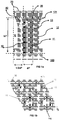
- Figure 1B shows the structure of Figure 1A in planar view.
- a single pillar 10 is shown as part of a structure of many pillars having an interdistance sP, e.g. with an interdistance sP between the pillar walls that ranges between 500 - 2500 nm.
- the electronic device comprises electronic circuitry (not depicted) equipped with a current collector 100 formed by a metal substrate having a face forming a high-aspect ratio structure of pillars 10.
- the walls have for example, an aspect ratio larger than 10 or even larger than 50.
- the pillars can e.g. be formed by a micropattern mask, so that isolated micro pillars are formed.
- the term pillars or micropillars is used to distinguish from 'dense' nanopillar structures.
- Such dense structures in contrast may have elongate tubes having diameter dimensions smaller than 300, or even smaller than 50 or 10 nm and with interdistances d smaller than about several hundreds nm, e.g. in the range of 50-300 nm, which are too densily packed without sufficient gap for conformally coating multilayer stacks on them.
- the micropillar structure may have pillar heights hP of more than 10 um, arbitrary elongate shapes and diameters dP at least larger than the said 10 nm, typically more than 100 nm and in this respect typically qualify as high aspect ratio structures.
- a pillar radius is therefor 0.5dP.
- the battery device comprises two current collectors 10, 20, one that supplies electrons by virtue of an oxidation process occurring at an electrode layer, in the example termed the anode 12, and a second one that consumes electrons by virtue of a reduction process occurring at that electrode, termed the cathode 11.
- the anode 12 is the "negative electrode” to which the positive current flows, from the cathode, being the "positive electrode”.
- the electrochemical relationship may be characterized by charge exchange between a negative electrode material and a positive electrode material, the negative electrode material having a workfunction or redox potential that is lower than the workfunction or redox potential of the positive electrode material.
- Thin film ion batteries including those of the thin film solid state lithium ion type, can be prepared from various deposition techniques to fabricate negative electrode 12 (e.g. LMNO), positive electrode 11 (e.g. LTO), and electrolyte materials 13 (e.g. LIPON) bonded together to form a battery device.
- Such techniques may typically include depositing thin films of such materials using vacuum deposition or other techniques that result in similar thin films, to produce the "thin film" batteries.
- a difference is marked between a coated pillar 110, and a 'bare' pillar 10, that forms the primary conductive structure on a planar surface 100.
- the top current collector 20 could be any organic or inorganic material. It can for example have some other extra functionality such as a current collector and may optionally, be electroplated over the pillars after the active layers of the battery stack are deposited. Also, the current collector can be used as a planarizing top that planarizes the high-aspect ratio structure.
- second electrode 12 is formed by covering the electrolyte layer 13; and top current collector layer 20 is formed in electrical contact with second electrode 12, wherein the second electrode 12 is shielded from the conductive structure 10 by an insulator 30 covering a part of said conductive structure 10 adjacent an end side thereof.
- an insulator 30 covering a part of said conductive structure 10 adjacent an end side thereof.
- the second electrode layer 12 is formed by covering the electrolyte layer 13 with a Lithium metal; and the top current collector layer 20 is brought in contact with the Lithium metal layer 12.
- the Lithium metal layer 12 is shielded from the conductive pillar 11 by an insulating cap 30 that shields the pillar top from the Lithium metal layer 12 and directs a charge/discharge current path in lateral direction.
- the pillar geometry 100 can be designed in such a way, that in fully plated condition of the anode (i.e. in charged condition of the battery) the Lithium metal is maximally expanded, while preventing radial stress against a neighbouring pillar 10.
- the pillar top is isolated by a resistive thin layer 30 of substantial resistivity, e.g. formed by Al2O3 deposition, in order to block a direct conduction between the pillar top and the top current collector, which could cause Lithium ions to migrate in axial direction.
- a resistive cap design Lithium ions substantially migrate in radial directions of the pillar, and form a substantially conformal electrode layer 12 that is electrically connected to the top current collector 20.
- the top current collector 20 is formed on top of the conductive structures partly covering the first electrode layer 11.
- the barrier may be formed on top of the electrolyte layer 13 as illustrated in Figure 2 .
- the layer 30 should have a high resistivity against ion transport.
- Another approach is to form a resistive barrier layer 30 directly on the metal pillar 10, as can be seen in Figure 1c . In that case the resistive layer blocks electron transport from the pillar 10 into the electrode 11, thereby it may redirect the electrochemical activity towards the lateral direction providing the electron conductivity of layer 11 is (substantially) lower than the ionic conductivity.
- Interface seed layer 40 forms a thin conductive structure that covers the ionconductive - non electroconductive - electrolyte. Accordingly, Lithium metal layer 12 can be provided in a step of depositing seed layer 40 on the electrolyte layer, and plating the seed layer 40 in a metal plating process with a Lithium metal.
- This conductive seed layer 40 may be selectively deposed on side walls of the electrolyte layer 13, and may comprise e.g. Ni, Cu, Pd, Pt, Au, Ti or combinations thereof.
- Layer 40 may be relatively thin from a few nm provided by thin film electroless deposition or plating or ALD or CVD techniques to about 10 nm. Thicker seed layers are possible if they are permeable for Li-ions, later when the battery undergoes charging and discharging operations.
- Interface seed layer 40 advantageously provides a direct electrical connection with top substrate 20.
- the Lithium metal may be directly applied in a deposition process by using an external lithium source, which could involve a lithium metal counter electrode, and plating said compound using an liquid electrolyte bath, so that it plates on the electrolyte 13 via said seed layer 40.
- FIG 2 depicts another scenario, wherein a plating process may extract the Lithium metal from a Lithiated i.e. 'loaded' first electrode layer 14 by providing an electrical voltage between the current metal pillars 10 of collector 100 and top substrate 20, via the seed layer 40. Accordingly, the plating process extracts the Lithium metal 12 from the first electrode layer 11 by providing an electrical voltage between the metal pillars 10 and the seed layer 40 - via top current collector 20. Note the difference with respect to the seed layer in Figure 1 , wherein the seed layer 40 remains in direct contact with the electrolyte 13, in contrast to the depicted scenario, wherein the seed layer 40 encloses the Lithium metal electrode layer 12.
- the seed layer could be from few nm to couple of 100nm thick.
- a 'Lithium free' manufacturing process can be provided, wherein Lithium metal forming the anode layer, is provided by providing a voltage difference between top current collector 20 and substrate 100, respectively via seed layer 40 and pillars 10 and thereby charging the battery device.
- the top current collector 20 extends partly into the inter pillar region, i.e. the seed layer 40 extends partly into the top current collector 20.
- the top current collector layer 20 comprises extend parts 200 along the upstanding walls of pillar 10.
- isolated pillar cap 30 may extend into the top current collector 20.
- the conductive layer 40 may be formed as a sacrificial layer, that disintegrates once the Lithium metal is plated with a thickness of e.g. 2-10 nm. It may also be formed as a current collector and scaffolding structure, for uniform plating at higher power, with a thickness of about 100 nm.
- the material 14 that is covered by the isolated cap 30 provides an excess of Lithium metal in the top current collector region.
- Figure 3a shows a further embodiment, wherein the Lithium metal is deposited as a transition structure 12 which may be partially porous, in such a way that it has improved electrical conductance near the top current collector, e.g. by an porous metal structure 15 extending from the top current collector 20 into the space between the pillars 10, and to accommodate lithium within the interpillar space S from a prelithiated cathode material during formation cycling.
- the porosity can be tuned e.g. by ramping up the charge speed after the film formation so far that diffusion limited transport is achieved, and dendritic-like lithium growth occurs.
- the top current collector layer extends along the upstanding walls alongside the insulating cap, defining a current flow away from the pillar top and providing a broadened electrical contact area with the top collector 20.By direct vapour deposition of the Lithium metal, a plating seed layer can be omitted. The techniques may be used in combination.
- the Lithium deposition 12 may be arranged by using filler particles 14, so that the lithium structure is regulated in density and porosity along the height of pillar 10. This can provide enhanced and stable electrical contact with the topcurrent collector, which can be further enhanced by the porous structure 15, which could be also in the form of conductive particles. It also prevents stress and controlled use of the Lithium metal within the interpillar space S.
- the interpillar space S separating adjacent conductive structures 10 is provided with a scaffolding structure 14, 15 so that the second electrode 12 and or top current collector 20 extends into the interspace structure, wherein said interspace structure comprises an electroconductive scaffold structure 14.
- anode layer 12 formed as a Lithium metal in plated condition is partially (pre)filled with nanoparticles (just) above the percolation threshold, so that the remaining space being (partially) filled with lithium metal.
- a nanoparticle may be a silicon nanoparticle, providing a hybrid anode.
- These particles may be formed with an electrically conductive shell.
- such filler particles may be Carbonaceous particles (e.g. Carbon Black) which may incorporated in a soft polymer matrix.
- Figure 4 shows a further enhancement, wherein said inter pillar space comprises a compression layer 50, that conforms to the second electrode.
- the said compression layer may be preferentially provided when the second electrode is Lithium depleted.
- the Lithium metal layer 12 is covered by a soft compression layer 50, which may accommodate stresses in the Lithium metal layer during charge and discharge. Especially with high C-rates such a layer is advantageous since it can exert a mechanical pressure similar to a 200 ring load on the anode layer 12 so as to accommodate large volume changes during the plating (battery charge) and stripping (battery discharge) of lithium metal.
- the layer 50 can be made of a compressible polymer, which may be a blend of polymer and electron conductive filler particles, so that a hybrid structure forms similar to Figure 3 .
- exemplary process steps are given to provide a Lithium battery with a substrate current collector formed of pillars on a substrate face of elongate and aligned structures on the substrate face with upstanding walls; wherein the walls are formed with a first electrode layer covering said walls, and a solid state electrolyte layer provided on the first electrode layer; and wherein a second electrode layer is formed by covering the electrolyte layer with a Lithium metal.
- a template substrate may be prepared with sacrificial template. This substrate can be for instance an aluminum or copper or silicon substrate. Pillars can be for instance made of a photoresist material, an aluminum oxide (AAO) layer, or a carbon nanotube/wire layer CNT/CNWs.
- a pillar structure 100 is provided, e.g. by a templating process, wherein pillars are grown templates that can be lithographically provided, for instance, in an Al2O3 substrate, wherein holes are back etched, and pillars are formed by a plating step.
- the pillar structure may be provided by conductive nanotubes, e.g. carbon nano tubes or the like.
- a smooth current collector layer may be deposited. e.g. Ni or Cu deposited by electroless plating or electroplating, or TiN by atomic layer deposition, which could be in the thickness range between 25 nm and 500 nm.
- a 100 nm thickness of the deposited layer is provided to ensure that the structure is stiff enough even for high aspect ratio pillars ( ⁇ >2 ⁇ m and >60 ⁇ m high).
- the base of the hollow pillars i.e. the non-structured flat area
- sacrificial substrate structures may be removed, e.g. by conventional etching steps, so that the current collector structure remains.
- the term structure is here indicated to provide a combined function of current collectors and electrodes, either in conformal laminate or in a scaffolding geometry.
- Layer thicknesses of the two sides of coating are adjusted in such a way that an optimal trade-off between capacity and rate performance match is reached between the two layers.
- Practical thicknesses of the electrode layers therefore vary between 100-3000 nm, and may be even smaller when merged within the collectors.
- Figure 5A shows a Lithium deposition method, that can be provided by a two step process.
- a first step an electrical voltage between a seed layer 12 and a counter electrode A is provided, that is separated from the seed layer by a liquid electrolyte E.
- the seed layer for 12 can be provided by lithium sputtering of the 3D structured battery foil 100.
- a metal 40 can be chosen of e.g. Ni, Cu, Pd, Pt, Au, Ti or combinations thereof.
- the sputtering process covers the solid state electrolyte layer 13 in the top and bottom parts of the battery foil 100. Accordingly the seed layer is provided as top layer exposed to the liquid electrolyte E.
- the counter electrode or electrolyte solution may acts as the lithium source as e.g. described in Henderson, "High rate and stable cycling of lithium metal anode", Nature Communications, February 2015, Volume 6, Article number 6362 and Takei, “Electrolytic deposition of lithium from non-aqueous solutions", Journal of Applied Electrochemistry September 1979, Volume 9, Issue 5, pp 587-593 .
- the anode layer 12 can be grown from bottom to top.
- Figure 5B shows a scaled up form, wherein the plating process is carried out for multiple two sided current collector structures that are electroplated by an opposed anodes.
- the foils are placed in a chemical bath 501 adjacent to counter electrode A.
- An electrolyte 502 provides ion conduction between the counter electrode and 3DTFB foil 100.
- the foil 100 is placed in such a way that only the area to be deposited is within the bath 501, matching with the position of counter electrode A. In this case, tuning of materials properties and geometries realizes the maximum possible conformal growth of the lithium layer onto the whole seed layer. This requires the electron transport kinetics through the seed layer 40 to be comparable with ion transport through the electrolyte.
- the electrolyte conductivity can be decreased (e.g. by decreasing salt concentration).
- the charge rate can be decreased.
- conformal growth can be obtained by formation cycling using the lithium in the cathode material.
- the seed layer should just be able to transport electrons over the whole pillar surface, provided the charge rates are sufficiently low to avoid rate limitation by ohmic loss along the pillar.
- FIG. 5C shows a further scale up, wherein it can be seen that a voltage connection 401 is provided to battery foil 100 in the following manner.
- Connection arms 401 provide electrical contact with conductive layer 302 provided on top of a foil edge 110 and supply a voltage over conductive layer 302 and the counter electrode A.
- Conductive layer 302 contacts a seed layer 40 of about 1-10 nm of e.g. Ni, Cu, Pd, Pt, Au, Ti is deposited on the structure 100 to form a optionally sacrificial electron conduction path for plating of lithium onto the pillars.
- This seed layer 40 can be provided by electroless plating or e.g.
- atomic layer deposition to provide Cu or TiN deposition or other electron conducting layers, prior to providing a seed layer of Lithium e.g. by sputtering.
- the electron conductivity of the seed layer should be > 10-3 S/cm.
- On foil edge 110 a relatively thick resist layer 301 is deposited to avoid shorts between the during pressure of the connection arm 401.
- the resist layer is covered with a conductive layer 302 contacting connection arm 401. The electrolyte in the bath can be continuously refreshed.
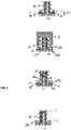
- Figure 6 and 7 show a plurality of embodiments, wherein a second electrode layer 12 is formed by covering the electrolyte layer 13 with a Lithium metal; and forming a top current collector layer in electrical contact with the Lithium metal layer, wherein the Lithium metal 12 layer is shielded from the conductive structure by an insulator 30, 35 covering a part of said conductive structure adjacent an end side thereof.
- a base-top collector 200 the Lithium anode layer 12, that growths during to battery charging, can simply expand away from the substrate 100.
- Figure 6 shows a first embodiment in steps IA, IB.
- a thin (ca. 30-300 nm) conductive layer 45 (metal) is selectively deposited at the base of the interpillar region as a base conductor 45, to provide the electrical current path for electroplating in consecutive steps. This can for example be provided by evaporation wherein by proper tuning a negligible amount will be deposited on the side walls of the pillars.
- a thin seed layer 40 of about 1-10 nm (120) of e.g. Ni, Cu, Pd, Pt, Au, Ti is deposited to form an [optionally sacrificial] electron conduction path for plating of lithium onto the pillars.
- Electron conductivity of the seed layer is preferably larger than 10-3 S/cm.
- Lithium metal is deposited at the bottom of the interpillar region S.
- This layer 12 of typically a few um acts, together with metal 45 as top current collector 200, i.e. it is an excess amount of lithium that transport electrons along the foil direction and does not significantly interfere with cell charge/discharge.
- the deposition can be achieved by electroplating -by an external source using an electrolyte bath or by a directional deposition technique like evaporation.
- the remaining interpillar space can be filled with a flexible material (polymer) 50 in the final embodiment IB.
- a flexible material (polymer) 50 in the final embodiment IB.
- the layer 50 can be may be made of a compressible electrolyte like a polymer Lithium ion conductive electrolyte e.g. a blend of polyethylene oxide PEO and a lithium salt LiX.
- a compressible electrolyte like a polymer Lithium ion conductive electrolyte e.g. a blend of polyethylene oxide PEO and a lithium salt LiX.
- FIG. 7 shows another embodiment in steps IIA, IIB.
- a top current collector 200 is provided at the base of the conductive structures with the insulator 35 shielding the top current collector from the substrate current collector 100.
- a thin (ca. 30-300 nm) conductive layer 46 may be selectively deposited at the base of the interpillar region S, to provide the electrical current path for electrodeposition in consecutive step e.g. by evaporation. Note that by evaporation the layer 46 will also be on top of the pillars, but by proper tuning to a negligible amount on the side walls of the pillars. Subsequently conductive seed layer 46 is used for electrodeposition of a barrier layer 35 at the base of the interpillar region. This insulator 35 (barrier layer) may further improve cycling stability by minimizing possible stresses due to electrochemical activity in the base part.
- the layer 35 has thickness of 20-200 nm and can partly cover the lower part of the pillar surface as well. Materials: e.g. Al2O3. Alternatively, the barrier layer 35 can be achieved by evaporation, in which case no seed layer 46 is necessary. On top of the barrier 35, a seed layer 45 for electroplating of lithium layer 12 may be deposited to form a top current collector 200 at the base of the conductive structures, similar to embodiment IA.
- the remaining interpillar space can be filled with a flexible material (polymer) 50 in the final embodiment IIB. This is preferably carried out when the Lithium layer is entirely depleted into the cathode layer 11.
- Embodiment III alternatively shows an additional seed layer 47 on top of barrier layer 35 for electrodeposition of top current collector 200 on the base of the interpillar region, typically a few microns thick.
- Seed layer 47 may be about 30-300 nm of e.g. Ni, Cu, Pt, Au, Ti deposited electrolessly. Alternatively TiN or other electron conducting layers with ALD.
- the top current collector 200 may be about 300nm-5 um of e.g. electrodeposited Ni, Cu, Pt or Ti.
- embodiment IV is shown with base-current collector 200 and both pillar end sides 30, 35 covered by isolator layers.
- the Lithium layer is shielded from the conductive structure 100 by insulators 30, 35 covering a base part of said conductive structure 100, respectively an end side of pillar 10. This prevents stress build up due to plating processes of Lithium near the end parts of the pillar 10.
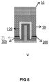
- Figure 8 shows another embodiment V similar to IIA, but wherein the interpillar space is filled with a flexible material 50 prior to plating the second electrode 12 and wherein layer 50 is in direct contact with counter electrode 55 acting as lithium source.
- the external source 55 electrically with the top current collector 200 plating of the second electrode 12 may be achieved as illustrated by embodiment IIB. Afterwards, the remaining external Lithium source 55 layer may be removed.
- insulator or barrier layer provided on any of the following:
- the barrier layer blocks ion transport, directing ion transport away from the end parts of the conductive structure 10.
- the barrier layer blocks electron transfer into the electrode, directing electron transport away from the end parts of the conductive structure 10. This works particularly well in conjunction with electrode material(s) like LixTiO2 and LTO having limited electron conductivity compared to ion transport.
- Examples of these thin-film batteries may be provided in an automobile, e.g. fabricated on the package or cover of automobile parts that use these batteries. Accordingly the metal substrate having the high aspect ratio structure may monolithically formed as a casing structure. There are other devices that have covers made of aluminium, where this concept may be applied. Alternatively a metal substrate may be stacked on an organic foil, i.e. containing a hydrocarbon content, for example, PEN, PET etc. or plastic mould structure. Even if the packages/covers of most of the devices today are moulded of plastic, still 10s of micrometers of aluminium can be electroless plated by ionic liquids on plastics to create the battery on it or in it.
- the high aspect ratio clusters may span an area smaller than 10e4 micrometer2; and the planar zones may be are formed as strips having a width larger than 50 micrometer, although other ranges can be suitably used to the same effect of clustering to enable easy flexing.
Landscapes
- Chemical & Material Sciences (AREA)
- Chemical Kinetics & Catalysis (AREA)
- Electrochemistry (AREA)
- General Chemical & Material Sciences (AREA)
- Engineering & Computer Science (AREA)
- Manufacturing & Machinery (AREA)
- Materials Engineering (AREA)
- Physics & Mathematics (AREA)
- Condensed Matter Physics & Semiconductors (AREA)
- General Physics & Mathematics (AREA)
- Inorganic Chemistry (AREA)
- Composite Materials (AREA)
- Cell Electrode Carriers And Collectors (AREA)
- Battery Electrode And Active Subsutance (AREA)
- Secondary Cells (AREA)
Description
- The present invention relates to a method of manufacturing a Lithium battery for electrochemical or electro-optical devices.
- For applications like portable electronics and automotive, e.g. for use in (hybrid) electric vehicles (EVs, PHEVs), battery systems are desired with optimal energy densities to provide minimal system weight and volume. To enable high energy densities, lithium metal based batteries (i.e. with lithium metal as anode) are appealing since the energy density of the metal can reach high levels of about 3800 mAh/g.
US6168884 discloses a planar design of a lithium metal anode that is formed in-situ during initial charge by plating lithium on an anode current collector, which does not form inter-metallic compounds with lithium. The anode current collector is sandwiched between a solid state electrolyte and an overlying layer. - It is also known to have a rechargeable Li-ion solid-state battery with a current collector of non-planar design. Thin-film battery structures of known type are disclosed e.g. in
WO2010032159 , the contents of which are included by reference, wherein for example all-solid state compositions are deposited on 3D micro-patterned structures. In this respect, where early battery structures utilize liquid electrolytes, all-solid state compositions utilize electrolytes of a solid state type, which are inherently safer in use. In these structures a large variety of materials are and have been used for the respective electrodes for example as disclosed inUS 20110117417 . -
DE102011121681 discloses a pillar geometry for a liquid electrolyte, wherein dendrites are prevented from forming on the pillar tops by isolating these. The pillars are extending in an electrolyte fluid or gel and distanced from a cathode sheet. -
WO2015126248 discloses a method of manufacturing a battery with a substrate current collector, wherein the method comprises: forming elongate and aligned electrically conductive structures on the substrate face with upstanding walls; wherein the walls are formed with a first electrode layer covering said walls, and a solid state electrolyte layer provided on the first electrode layer; and wherein a second electrode is formed by covering the electrolyte layer; and forming a top current collector layer in electrical contact with the second electrode. - In discharging battery mode, the anode is the "negative electrode" to which the positive current flows, from the cathode, being the "positive electrode". During charge these functions are reversed. Irrespective charging mode, the electrochemical relationship may be characterized by charge exchange between a negative electrode material and a positive electrode material, the negative electrode material having a workfunction or redox potential that is lower than the workfunction or redox potential of the positive electrode material.
- For example, known negative electrode (anode) materials are Li4Ti5O12 (LTO); LiC6 (Graphite); Li4.4 Si (Silicon) and Li4.4Ge (Germanium) known positive electrode (cathode) materials are LiCOO2 (LCO), LiCoPO4, (doped) LiMn2O4 (LMO), LiMnPO4, LiFePO4 (LFP), LiFePO4F(LFPF), LiCO1/3Ni1/3Mn1/3O2 (LCNMO), Sulphur or Sulphur based compounds like LixS.
- Known (solid state) electrolytes might include Garnets such as Li7La3Zr2O12 (LLZO), Perovskites such as La0.57Li0.33TiO3 (LLTO), lithium iodide (LiI), lithium phosphate (Li3PO4) and lithium phosphorus oxynitride (LiPON). In addition, lithium salts, such as LiPF6, LiBF4 or LiClO4 in an organic solvent, such as ethylene carbonate, dimethyl carbonate, diethyl carbonate, propylene carbonate are known to have a typical conductivity of about 10 mS/cm at RT. The electrolyte decomposes on initial charging and forms a solid layer called the solid electrolyte interphase (SEI).
- Solid polymer separators like polyethylene oxide (PEO) may also be included, such polymers having transport capacity often due to having a lithium salt disposed therein as known in the state of the art. Work has also been performed with lithium and halide materials, particularly, in some examples, a lithium aluminum tetrahalide such as lithium aluminum tetrafluoride (LiAlF4).
- Once such structures are made on a bendable metal foil, they can be manufactured in large-scale processes, e.g. a roll-to-roll process where the following can be done: 1) Coiling, winding or stacking it to increase the energy or power density per unit volume. 2) Integrating it on flexible devices like flexible displays, signage etc.
- Although high-aspect ratio structures can be made in nanometer scale the height or depth of these high-aspect ratio structures need to be in the microns range for delivering enough charge capacity for the battery. The reason why these structures are preferred is due to the easy accessibility of their entire surface. In the prior art many methods to produce these are non-economical (e.g. involving silicon microfabrication and long-time electrodeposition). Moreover, to do any of these, the design of the stack is in need for optimization because otherwise while winding or flexing, the pillar structure could be damaged inhibiting proper electrochemical action of the device. Furthermore, it has come to the attention that existing solid state (e.g.) Li-based intercalation electrolytes induce stress in the high-aspect ratio structures that may limit lifetime and reduce the number of cycle periods. A challenge exists to minimize the relative amount of electrochemically inactive electronic current collectors without compromising on the rate performance. It is aimed to provide a method and structure for a 3D thin film battery design, having an all-solid state structure to provide a design with both inherent safety and high energy densities.
- It is an object of the invention to provide a method for producing an electronic device having a current collector capable of a high specific charge collecting area and power, having a proper dimensioning but is also achieved using a simple and fast technique and resulting in a robust design.
- To this end, according to an aspect a method is provided of manufacturing a battery according to
claim 1. - The pillars function as current collectors for the battery structure in a laminate, which current collectors are electrically connected through a base substrate. Between adjacent pillars, an aspect ratio of a height dimension and the pillar interdistance, i.e. a length dimension normal to the walls coplanar along the base, is relatively high, that is, higher than 50, or even higher than 80 or even more than 100. In a typical arrangement, the pillars may have height dimensions, i.e. a height separating a base plane from a planar surface of about 25-200 micrometer, preferably 50-100 micrometer wherein the length dimensions, i.e. the length separating opposing pillars, can be in the order of 1-10 micrometer, preferably 2-4 micrometer. For such structures, the substrate as presently disclosed is electrically conductive with a surface area of the current collector that is significantly increased, which enhances the charge collecting capacity of the current collector. Moreover, for such structures, it is possible to apply a conformal multilayer coating without compromising the functionality of the multilayer coating. Examples of such functionality may be multilayers such as a battery multilayer or photovoltaic multilayer or single layer coatings.
- In addition, according to an aspect of the invention, for such high-aspect ratio structures optimal current collecting performance may be provided in the form of a coated pillar wherein the high-aspect ratio structure comprises metal or metalized pillars having a radius of curvature larger than 50 nanometer. An aspect of improved performance is a trade-off that is found by a density of the high-aspect ratio structure demanding smaller pitches and the surrounding conformal coating. In this respect, electrode thicknesses in the battery multilayer may be varied and are correlated to match their volumetric storage capacities for Lithium-ions while charging and/or discharging. A known matching relationship is governed by a C-rate number, known in the art. A C-rate is a measure of the rate at which a battery is charged or discharged relative to its maximum capacity. For example the capacity of the electrode layers at a certain C-rate are matched by controlling layer thickness and material composition.
- Another aspect of the invention is that a 'conformal coating' is a coating that may comprise a plurality of layers that at least conformally coat the pillars of the high aspect ratio structure. Furthermore, in this application, a 'first electrode layer' may be part of a laminate and may be a bottom layer, i.e. the layer with the smallest radius of curvature. The 'second electrode' may be used to indicate a top layer of a laminate, i.e. the layer with the highest radius of curvature. It is noted that a laminate is not essential, since the electrode structures may be merged into the collector structures as porous complex structures. In such embodiments, an electrolyte layer is provided between electrode structures that are combined with current collector structures.
- It is noted that in
US2009214956 a structure is proposed wherein electrolyte material is conformally coated onto conducting nanowires and wherein cathode material, in electrical connection with a second conductive material, is interpenetrated between electrolyte-coated nanowires. - With thickness is meant 'average thickness' which may render an equivalent function of a certain mathematical thickness. In the application, where layers are coated, it is intended that these coatings at their functional locations are substantially conformal, but this is not necessary, as long as a functional layer is designed to have a thickness where a tradeoff is reached between internal resistance, and energy density. In the specification, depending on context, functional layers may not be in direct contact with other functional structures, but may have intermediate layers or structures in between that may enhance functionality. In that respect, the skilled person will understand that where it is described, for example, that an electrode layer is 'a layer', 'in contact' with a charge collector, such would be interpreted as 'in electrical contact' not excluding a possible Lithium diffusion barrier layer, current collecting layer, process protection layer etc. enhancing functionality. This similarly counts for electrolyte layers 'in contact' with negative or positive electrode layers.
- These and other aspects of the invention will be discussed in more detail with reference to drawings, wherein like reference numerals refer to like elements. It will be appreciated that the drawings are presented for illustrative purposes and may not be used for limiting the scope of the appended claims.
-
-
Figure 1A shows a geometric structure of an embodiment in cross sectional view; -
Figure 1B the structure ofFigure 1A in planar view; -
Figure 1C shows an alternative geometric structure of an embodiment in cross sectional view; -
Figure 2 shows a further embodiment in cross sectional view; -
Figure 3A and3B show further embodiments in cross sectional view according to an aspect of the invention; -
Figure 4 shows yet a further embodiment in cross sectional view according to an aspect of the invention; -
Figure 5A , B and C show exemplary process steps for forming a second electrode layer by covering the electrolyte layer with a Lithium metal; -
Figure 6 shows yet a further embodiment in cross sectional view according to an aspect of the invention; -
Figure 7 shows yet a further embodiment in cross sectional view according to an aspect of the invention; -
Figure 8 shows further embodiments in cross sectional view according to an aspect of the invention. - In the following examples in more detail aspects of the invention will be illustrated in the form of an electrochemical device, more specifically a battery device, for instance of a lithium ion type, more specifically having a 3D collector structure for enhancing the charge collecting specific area of the collector, that is in electrical contact with battery multilayer, in particular, a negative electrode layer thereof.
-
Figure 1a shows a geometric structure of an embodiment in cross sectional view where electricallyconductive pillars 10 are formed on thesubstrate face 100. A general challenge for batteries is to minimize the relative amount of electrochemically inactive electronic current collectors (CC) without compromising on the rate performance. The 3D structured bottom CC - e.g. pillars, holes or plates/trenches - imposes a relative large amount of inactive material in terms of volume and weight, as their dimensions (aspect ratios) are bound by technical limitations. In addition, for 2D-confined structures such as pillars a too small radius can force the bottom electrode to approach non-favorable dimensions, i.e. a too thick layer with limited diffusion. Moreover, fabrication of very thin and high aspect ratio pillars is a processing challenge. The final spacing between pillars (after depositing 3DTFB stack) is typically filled with a topcurrent collector 20. -
Figure 1B shows the structure ofFigure 1A in planar view. In the figure, asingle pillar 10 is shown as part of a structure of many pillars having an interdistance sP, e.g. with an interdistance sP between the pillar walls that ranges between 500 - 2500 nm. - The electronic device comprises electronic circuitry (not depicted) equipped with a
current collector 100 formed by a metal substrate having a face forming a high-aspect ratio structure ofpillars 10. The walls have for example, an aspect ratio larger than 10 or even larger than 50. The pillars can e.g. be formed by a micropattern mask, so that isolated micro pillars are formed. In the specification, the term pillars or micropillars is used to distinguish from 'dense' nanopillar structures. Such dense structures, in contrast may have elongate tubes having diameter dimensions smaller than 300, or even smaller than 50 or 10 nm and with interdistances d smaller than about several hundreds nm, e.g. in the range of 50-300 nm, which are too densily packed without sufficient gap for conformally coating multilayer stacks on them. - The micropillar structure may have pillar heights hP of more than 10 um, arbitrary elongate shapes and diameters dP at least larger than the said 10 nm, typically more than 100 nm and in this respect typically qualify as high aspect ratio structures. Herebelow, a pillar radius is therefor 0.5dP.
- In its simplest conceptualization, the battery device comprises two
current collectors anode 12, and a second one that consumes electrons by virtue of a reduction process occurring at that electrode, termed thecathode 11. In discharging battery mode, theanode 12 is the "negative electrode" to which the positive current flows, from the cathode, being the "positive electrode". During charge these functions are reversed. Irrespective of charging mode, the electrochemical relationship may be characterized by charge exchange between a negative electrode material and a positive electrode material, the negative electrode material having a workfunction or redox potential that is lower than the workfunction or redox potential of the positive electrode material. - Thin film ion batteries, including those of the thin film solid state lithium ion type, can be prepared from various deposition techniques to fabricate negative electrode 12 (e.g. LMNO), positive electrode 11 (e.g. LTO), and electrolyte materials 13 (e.g. LIPON) bonded together to form a battery device. Such techniques may typically include depositing thin films of such materials using vacuum deposition or other techniques that result in similar thin films, to produce the "thin film" batteries. In the Figures, a difference is marked between a
coated pillar 110, and a 'bare'pillar 10, that forms the primary conductive structure on aplanar surface 100. - Thin film batteries are often employed in applications in which space and weight may preferably be conserved and extremely long cycle life may be desired. The top
current collector 20 could be any organic or inorganic material. It can for example have some other extra functionality such as a current collector and may optionally, be electroplated over the pillars after the active layers of the battery stack are deposited. Also, the current collector can be used as a planarizing top that planarizes the high-aspect ratio structure. - According to the invention,
second electrode 12 is formed by covering theelectrolyte layer 13; and topcurrent collector layer 20 is formed in electrical contact withsecond electrode 12, wherein thesecond electrode 12 is shielded from theconductive structure 10 by aninsulator 30 covering a part of saidconductive structure 10 adjacent an end side thereof. By shielding a part of the conductive structure, the (ion) current path between first and second electrode is directed away from the end parts of the conductive structure. This results in less electrochemical activity at the end parts of the conductive structure mitigating uneven expansions of the electrode materials, which can be typically formed by methods such as plating or intercalating or spray coating or gas phase deposition process. - According to a more specific aspect, as can be seen in
Figure 1 , thesecond electrode layer 12 is formed by covering theelectrolyte layer 13 with a Lithium metal; and the topcurrent collector layer 20 is brought in contact with theLithium metal layer 12. TheLithium metal layer 12 is shielded from theconductive pillar 11 by an insulatingcap 30 that shields the pillar top from theLithium metal layer 12 and directs a charge/discharge current path in lateral direction. - The
pillar geometry 100 can be designed in such a way, that in fully plated condition of the anode (i.e. in charged condition of the battery) the Lithium metal is maximally expanded, while preventing radial stress against a neighbouringpillar 10. - In order to prevent stress that could be built up by plating Lithium metal in the axial direction, the pillar top is isolated by a resistive
thin layer 30 of substantial resistivity, e.g. formed by Al2O3 deposition, in order to block a direct conduction between the pillar top and the top current collector, which could cause Lithium ions to migrate in axial direction. By the resistive cap design Lithium ions substantially migrate in radial directions of the pillar, and form a substantiallyconformal electrode layer 12 that is electrically connected to the topcurrent collector 20. In the shown Figure, the topcurrent collector 20 is formed on top of the conductive structures partly covering thefirst electrode layer 11. Alternatively the barrier may be formed on top of theelectrolyte layer 13 as illustrated inFigure 2 . In both cases thelayer 30 should have a high resistivity against ion transport. Another approach is to form aresistive barrier layer 30 directly on themetal pillar 10, as can be seen inFigure 1c . In that case the resistive layer blocks electron transport from thepillar 10 into theelectrode 11, thereby it may redirect the electrochemical activity towards the lateral direction providing the electron conductivity oflayer 11 is (substantially) lower than the ionic conductivity. - In that case a further advantage is provided of having
excess Lithium 121 available near the pillar top, which favours an electrical connection with the top substrate. The resistive barrier accordingly decreases electrochemical activity at the top of thepillar 10. This, together with partial top current collector penetration and a lithium excess region, maximizes contact and minimizes the volumetric stresses in this region for better cycling stability. - The resistance of the barrier in such a way that lithium transport along that layer is preferred (Arrow A), so for a fully
lithiated cathode 11 prior formation part of the lithium at the top diffuse towards the lower lying region during charge. -
Interface seed layer 40 forms a thin conductive structure that covers the ionconductive - non electroconductive - electrolyte. Accordingly,Lithium metal layer 12 can be provided in a step of depositingseed layer 40 on the electrolyte layer, and plating theseed layer 40 in a metal plating process with a Lithium metal. Thisconductive seed layer 40 may be selectively deposed on side walls of theelectrolyte layer 13, and may comprise e.g. Ni, Cu, Pd, Pt, Au, Ti or combinations thereof.Layer 40 may be relatively thin from a few nm provided by thin film electroless deposition or plating or ALD or CVD techniques to about 10 nm. Thicker seed layers are possible if they are permeable for Li-ions, later when the battery undergoes charging and discharging operations. -
Interface seed layer 40 advantageously provides a direct electrical connection withtop substrate 20. In one scenario, depicted here, the Lithium metal may be directly applied in a deposition process by using an external lithium source, which could involve a lithium metal counter electrode, and plating said compound using an liquid electrolyte bath, so that it plates on theelectrolyte 13 via saidseed layer 40. -
Figure 2 depicts another scenario, wherein a plating process may extract the Lithium metal from a Lithiated i.e. 'loaded'first electrode layer 14 by providing an electrical voltage between thecurrent metal pillars 10 ofcollector 100 andtop substrate 20, via theseed layer 40. Accordingly, the plating process extracts theLithium metal 12 from thefirst electrode layer 11 by providing an electrical voltage between themetal pillars 10 and the seed layer 40 - via topcurrent collector 20. Note the difference with respect to the seed layer inFigure 1 , wherein theseed layer 40 remains in direct contact with theelectrolyte 13, in contrast to the depicted scenario, wherein theseed layer 40 encloses the Lithiummetal electrode layer 12. Moreover, in this embodiment, the seed layer could be from few nm to couple of 100nm thick. In this way, a 'Lithium free' manufacturing process can be provided, wherein Lithium metal forming the anode layer, is provided by providing a voltage difference between topcurrent collector 20 andsubstrate 100, respectively viaseed layer 40 andpillars 10 and thereby charging the battery device. As a further enhancement, to provide faster and improved electrical contact, the topcurrent collector 20 extends partly into the inter pillar region, i.e. theseed layer 40 extends partly into the topcurrent collector 20. Accordingly, the topcurrent collector layer 20 comprises extendparts 200 along the upstanding walls ofpillar 10. Similarly,isolated pillar cap 30 may extend into the topcurrent collector 20. Theconductive layer 40 may be formed as a sacrificial layer, that disintegrates once the Lithium metal is plated with a thickness of e.g. 2-10 nm. It may also be formed as a current collector and scaffolding structure, for uniform plating at higher power, with a thickness of about 100 nm. Advantageously, thematerial 14 that is covered by theisolated cap 30 provides an excess of Lithium metal in the top current collector region. -
Figure 3a shows a further embodiment, wherein the Lithium metal is deposited as atransition structure 12 which may be partially porous, in such a way that it has improved electrical conductance near the top current collector, e.g. by anporous metal structure 15 extending from the topcurrent collector 20 into the space between thepillars 10, and to accommodate lithium within the interpillar space S from a prelithiated cathode material during formation cycling. The porosity can be tuned e.g. by ramping up the charge speed after the film formation so far that diffusion limited transport is achieved, and dendritic-like lithium growth occurs. - Accordingly the top current collector layer extends along the upstanding walls alongside the insulating cap, defining a current flow away from the pillar top and providing a broadened electrical contact area with the top collector 20.By direct vapour deposition of the Lithium metal, a plating seed layer can be omitted. The techniques may be used in combination.
- In another example shown in
Figure 3B , theLithium deposition 12 may be arranged by usingfiller particles 14, so that the lithium structure is regulated in density and porosity along the height ofpillar 10. This can provide enhanced and stable electrical contact with the topcurrent collector, which can be further enhanced by theporous structure 15, which could be also in the form of conductive particles. It also prevents stress and controlled use of the Lithium metal within the interpillar space S. - Accordingly, the interpillar space S separating adjacent
conductive structures 10 is provided with ascaffolding structure second electrode 12 and or topcurrent collector 20 extends into the interspace structure, wherein said interspace structure comprises anelectroconductive scaffold structure 14. Forexample anode layer 12 formed as a Lithium metal in plated condition, is partially (pre)filled with nanoparticles (just) above the percolation threshold, so that the remaining space being (partially) filled with lithium metal. Such a nanoparticle may be a silicon nanoparticle, providing a hybrid anode. These particles may be formed with an electrically conductive shell. In another example, such filler particles may be Carbonaceous particles (e.g. Carbon Black) which may incorporated in a soft polymer matrix. -
Figure 4 shows a further enhancement, wherein said inter pillar space comprises acompression layer 50, that conforms to the second electrode. For a lithiated or loaded first electrode the said compression layer may be preferentially provided when the second electrode is Lithium depleted. TheLithium metal layer 12 is covered by asoft compression layer 50, which may accommodate stresses in the Lithium metal layer during charge and discharge. Especially with high C-rates such a layer is advantageous since it can exert a mechanical pressure similar to a 200 ring load on theanode layer 12 so as to accommodate large volume changes during the plating (battery charge) and stripping (battery discharge) of lithium metal. Thelayer 50 can be made of a compressible polymer, which may be a blend of polymer and electron conductive filler particles, so that a hybrid structure forms similar toFigure 3 . - In the following, exemplary process steps are given to provide a Lithium battery with a substrate current collector formed of pillars on a substrate face of elongate and aligned structures on the substrate face with upstanding walls; wherein the walls are formed with a first electrode layer covering said walls, and a solid state electrolyte layer provided on the first electrode layer; and wherein a second electrode layer is formed by covering the electrolyte layer with a Lithium metal. In a first process step a template substrate may be prepared with sacrificial template. This substrate can be for instance an aluminum or copper or silicon substrate. Pillars can be for instance made of a photoresist material, an aluminum oxide (AAO) layer, or a carbon nanotube/wire layer CNT/CNWs. These structures may be provided by a combination of process steps known to the skilled person. For example, in a first step, a
pillar structure 100 is provided, e.g. by a templating process, wherein pillars are grown templates that can be lithographically provided, for instance, in an Al2O3 substrate, wherein holes are back etched, and pillars are formed by a plating step. Alternatively, the pillar structure may be provided by conductive nanotubes, e.g. carbon nano tubes or the like. In a second process step a smooth current collector layer may be deposited. e.g. Ni or Cu deposited by electroless plating or electroplating, or TiN by atomic layer deposition, which could be in the thickness range between 25 nm and 500 nm. Preferably, a 100 nm thickness of the deposited layer is provided to ensure that the structure is stiff enough even for high aspect ratio pillars (Ø >2µm and >60µm high). The base of the hollow pillars (i.e. the non-structured flat area) can be made thicker (∼5µm) for handling. - Next, in a further process step sacrificial substrate structures may be removed, e.g. by conventional etching steps, so that the current collector structure remains.
- The term structure is here indicated to provide a combined function of current collectors and electrodes, either in conformal laminate or in a scaffolding geometry. Layer thicknesses of the two sides of coating are adjusted in such a way that an optimal trade-off between capacity and rate performance match is reached between the two layers. Practical thicknesses of the electrode layers therefore vary between 100-3000 nm, and may be even smaller when merged within the collectors.
-
Figure 5A shows a Lithium deposition method, that can be provided by a two step process. In a first step an electrical voltage between aseed layer 12 and a counter electrode A is provided, that is separated from the seed layer by a liquid electrolyte E. The seed layer for 12 can be provided by lithium sputtering of the 3D structuredbattery foil 100. Alternatively ametal 40 can be chosen of e.g. Ni, Cu, Pd, Pt, Au, Ti or combinations thereof. - The sputtering process covers the solid
state electrolyte layer 13 in the top and bottom parts of thebattery foil 100. Accordingly the seed layer is provided as top layer exposed to the liquid electrolyte E. The counter electrode or electrolyte solution may acts as the lithium source as e.g. described in Henderson, "High rate and stable cycling of lithium metal anode", Nature Communications, February 2015, Volume 6, Article number 6362 and Takei, "Electrolytic deposition of lithium from non-aqueous solutions", Journal of Applied Electrochemistry September 1979, Volume 9, Issue 5, pp 587-593. By electrically connecting the bottom parts of the Lithium anode, theanode layer 12 can be grown from bottom to top. -
Figure 5B shows a scaled up form, wherein the plating process is carried out for multiple two sided current collector structures that are electroplated by an opposed anodes. The foils are placed in achemical bath 501 adjacent to counter electrode A. Anelectrolyte 502 provides ion conduction between the counter electrode and3DTFB foil 100. Thefoil 100 is placed in such a way that only the area to be deposited is within thebath 501, matching with the position of counter electrode A. In this case, tuning of materials properties and geometries realizes the maximum possible conformal growth of the lithium layer onto the whole seed layer. This requires the electron transport kinetics through theseed layer 40 to be comparable with ion transport through the electrolyte. To achieve this, the electrolyte conductivity can be decreased (e.g. by decreasing salt concentration). Also, the charge rate can be decreased. Alternatively conformal growth can be obtained by formation cycling using the lithium in the cathode material. In this case the seed layer should just be able to transport electrons over the whole pillar surface, provided the charge rates are sufficiently low to avoid rate limitation by ohmic loss along the pillar. -
Figure 5C shows a further scale up, wherein it can be seen that avoltage connection 401 is provided tobattery foil 100 in the following manner.Connection arms 401 provide electrical contact withconductive layer 302 provided on top of afoil edge 110 and supply a voltage overconductive layer 302 and the counter electrodeA. Conductive layer 302 contacts aseed layer 40 of about 1-10 nm of e.g. Ni, Cu, Pd, Pt, Au, Ti is deposited on thestructure 100 to form a optionally sacrificial electron conduction path for plating of lithium onto the pillars. Thisseed layer 40 can be provided by electroless plating or e.g. atomic layer deposition to provide Cu or TiN deposition or other electron conducting layers, prior to providing a seed layer of Lithium e.g. by sputtering. The electron conductivity of the seed layer should be > 10-3 S/cm. On foil edge 110 a relatively thick resistlayer 301 is deposited to avoid shorts between the during pressure of theconnection arm 401. The resist layer is covered with aconductive layer 302 contactingconnection arm 401. The electrolyte in the bath can be continuously refreshed. -
Figure 6 and7 show a plurality of embodiments, wherein asecond electrode layer 12 is formed by covering theelectrolyte layer 13 with a Lithium metal; and forming a top current collector layer in electrical contact with the Lithium metal layer, wherein theLithium metal 12 layer is shielded from the conductive structure by aninsulator top collector 200, theLithium anode layer 12, that growths during to battery charging, can simply expand away from thesubstrate 100. -
Figure 6 shows a first embodiment in steps IA, IB. In a first step, a thin (ca. 30-300 nm) conductive layer 45 (metal) is selectively deposited at the base of the interpillar region as abase conductor 45, to provide the electrical current path for electroplating in consecutive steps. This can for example be provided by evaporation wherein by proper tuning a negligible amount will be deposited on the side walls of the pillars. On top of the structure athin seed layer 40 of about 1-10 nm (120) of e.g. Ni, Cu, Pd, Pt, Au, Ti is deposited to form an [optionally sacrificial] electron conduction path for plating of lithium onto the pillars. This can be provided by electroless plating or alternatively by atomic layer deposition, to provide a Cu, TiN or other electron conducting layers. Electron conductivity of the seed layer is preferably larger than 10-3 S/cm. Subsequently Lithium metal is deposited at the bottom of the interpillar region S. Thislayer 12 of typically a few um acts, together withmetal 45 as topcurrent collector 200, i.e. it is an excess amount of lithium that transport electrons along the foil direction and does not significantly interfere with cell charge/discharge. The deposition can be achieved by electroplating -by an external source using an electrolyte bath or by a directional deposition technique like evaporation. By tuning the electroplating process, selective growth of the lithium layer at the base of the interpillar structure can be provided , and not onto the [whole]seed layer 40. Selective - preferably conformal - growth is achieved if the ion transport kinetics through the electrolyte E is effectively faster than electron transport through the seed layer. This can be tuned by proper selection of the electrolyte (type, salt concentration, ..), the current rate of electroplating, and the combination of layer thickness and material type of theconductive layer 45 andseed layer 40.Conductive layer 45 may be omitted when thelithium layer 12 is evaporated in stead of plated. Also a combination is possible by cyclic plating. - Finally, it shows that the remaining interpillar space can be filled with a flexible material (polymer) 50 in the final embodiment IB. This is preferably carried out when the Lithium layer is entirely depleted into the
cathode layer 11. Alternatively, thelayer 50 can be may be made of a compressible electrolyte like a polymer Lithium ion conductive electrolyte e.g. a blend of polyethylene oxide PEO and a lithium salt LiX. This has the advantage that the compressible layer can be provided prior to Lithium depletion and can function as an electrolyte, e.g. via an external Lithium source that may be temporarily provided on top of the compressible layer 59. -
Figure 7 shows another embodiment in steps IIA, IIB. Here a topcurrent collector 200 is provided at the base of the conductive structures with theinsulator 35 shielding the top current collector from the substratecurrent collector 100. - In a first step, a thin (ca. 30-300 nm) conductive layer 46 (metal) may be selectively deposited at the base of the interpillar region S, to provide the electrical current path for electrodeposition in consecutive step e.g. by evaporation. Note that by evaporation the
layer 46 will also be on top of the pillars, but by proper tuning to a negligible amount on the side walls of the pillars. Subsequentlyconductive seed layer 46 is used for electrodeposition of abarrier layer 35 at the base of the interpillar region. This insulator 35 (barrier layer) may further improve cycling stability by minimizing possible stresses due to electrochemical activity in the base part. Thelayer 35 has thickness of 20-200 nm and can partly cover the lower part of the pillar surface as well. Materials: e.g. Al2O3. Alternatively, thebarrier layer 35 can be achieved by evaporation, in which case noseed layer 46 is necessary. On top of thebarrier 35, aseed layer 45 for electroplating oflithium layer 12 may be deposited to form a topcurrent collector 200 at the base of the conductive structures, similar to embodiment IA. - Finally, it shows that the remaining interpillar space can be filled with a flexible material (polymer) 50 in the final embodiment IIB. This is preferably carried out when the Lithium layer is entirely depleted into the
cathode layer 11. - Embodiment III alternatively shows an
additional seed layer 47 on top ofbarrier layer 35 for electrodeposition of topcurrent collector 200 on the base of the interpillar region, typically a few microns thick.Seed layer 47 may be about 30-300 nm of e.g. Ni, Cu, Pt, Au, Ti deposited electrolessly. Alternatively TiN or other electron conducting layers with ALD. The topcurrent collector 200 may be about 300nm-5 um of e.g. electrodeposited Ni, Cu, Pt or Ti. - As an alternative, embodiment IV is shown with base-
current collector 200 and both pillar end sides 30, 35 covered by isolator layers. In this embodiment, the Lithium layer is shielded from theconductive structure 100 byinsulators conductive structure 100, respectively an end side ofpillar 10. This prevents stress build up due to plating processes of Lithium near the end parts of thepillar 10. -
Figure 8 shows another embodiment V similar to IIA, but wherein the interpillar space is filled with aflexible material 50 prior to plating thesecond electrode 12 and whereinlayer 50 is in direct contact withcounter electrode 55 acting as lithium source. By connecting theexternal source 55 electrically with the topcurrent collector 200 plating of thesecond electrode 12 may be achieved as illustrated by embodiment IIB. Afterwards, the remainingexternal Lithium source 55 layer may be removed. - Further examples are an insulator or barrier layer provided on any of the following:
- 1. On top of
first cathode electrode 11 - 2. On top of
electrolyte 13 - 3. On top of
pillar 10 - 4. On top of
second anode electrode 12 - In case 1&2, the barrier layer blocks ion transport, directing ion transport away from the end parts of the
conductive structure 10. - In case 3&4, the barrier layer blocks electron transfer into the electrode, directing electron transport away from the end parts of the
conductive structure 10. This works particularly well in conjunction with electrode material(s) like LixTiO2 and LTO having limited electron conductivity compared to ion transport. - Examples of these thin-film batteries may be provided in an automobile, e.g. fabricated on the package or cover of automobile parts that use these batteries. Accordingly the metal substrate having the high aspect ratio structure may monolithically formed as a casing structure. There are other devices that have covers made of aluminium, where this concept may be applied. Alternatively a metal substrate may be stacked on an organic foil, i.e. containing a hydrocarbon content, for example, PEN, PET etc. or plastic mould structure. Even if the packages/covers of most of the devices today are moulded of plastic, still 10s of micrometers of aluminium can be electroless plated by ionic liquids on plastics to create the battery on it or in it.
- Optionally, in order to enable easy flexing, instead of having the pillars all over the substrate foil, isolated islands of pillar-clusters be patterned in a metal foil to form an integral part of it. In an example, the high aspect ratio clusters may span an area smaller than 10e4 micrometer2; and the planar zones may be are formed as strips having a width larger than 50 micrometer, although other ranges can be suitably used to the same effect of clustering to enable easy flexing. In order to make such batteries cost-effective, it is advantageous to transfer this technology to large area metal foils e.g. for roll-to-roll processing.
Claims (20)
- A method of manufacturing a battery with a substrate current collector, wherein the method comprises: forming elongate and aligned electrically conductive structures (10) on the substrate face (100) with upstanding walls; wherein the walls are formed with a first electrode layer (11) covering said walls, and a solid state electrolyte layer (13) provided on the first electrode layer; and wherein a second electrode (12) is formed by covering the electrolyte layer; and forming a top current collector layer (20) in electrical contact with the second electrode, characterized in that the second electrode is shielded from the conductive structure by an insulator (30) covering a part of said conductive structure adjacent an end side thereof to prevent an ion transport path between the first and second electrode thereby mitigating stress build up near the end side of the conductive structure.
- A method according to claim 1, wherein the top current collector (20) is formed on top of the conductive structures on the substrate face.
- A method according to claim 1, wherein the top current collector (20) is provided at the base of the conductive structures with the insulator (30) shielding the top from the substrate current collector.
- A method according to any of claims 1- 3, wherein the insulator (30) partly covers the first electrode layer.
- A method according to any of the preceding claims, wherein the second electrode layer is a Lithium metal layer.
- A method according to claim 5 wherein the Lithium metal layer is provided in a step of depositing a seed layer on the electrolyte layer, and plating the seed layer in a metal plating process with a Lithium metal.
- A method according to claim 6, wherein the plating process extracts the Lithium metal from the first electrode layer by providing an electrical voltage between the metal pillars and the seed layer.
- A method according to claim 6 or 7, wherein the plating process is provided by providing an electrical voltage between the seed layer and a counter electrode that is separated from the seed layer; wherein the counter electrode and/or electrolyte in contact with the seed layer comprise a Lithium source.
- A method according to claim 1, wherein the top current collector layer extends along the upstanding walls.
- A method according to claim 1, wherein an interspace structure is provided separating adjacent conductive structures so that the second electrode extends into the interspace structure, wherein said interspace structure comprises an electroconductive scaffold.
- A method according to claim 10, wherein the electroconductive scaffold is formed by a hollow or porous metal structure
- A method according to claim 10, wherein the electroconductive scaffold is formed by conductive nanoparticles.
- A method according to claim 1, wherein an interspace structure is provided separating adjacent conductive structures so that the second electrode extends into the interspace structure, wherein said interspace structure comprises a compression layer, that conforms to the second electrode, said compression layer provided when the second electrode is Lithium depleted.
- A method according to claim 1, wherein an interspace structure between the conductive structures comprises a compression layer, that conforms to the second electrode, said compression layer comprising an Lithium ion conductive material to provide the second electrode.
- A battery with a substrate current collector, comprising elongate and aligned electrically conductive structures (10) on the substrate face (100) with upstanding walls; wherein the walls are formed with a first electrode layer (11) covering said walls, and a solid state electrolyte layer (13) provided on the first electrode layer; and wherein a second electrode (12) is formed by covering the electrolyte layer; and wherein a top current collector (20) layer is in electrical contact with the second electrode, characterized in that the second electrode is shielded from the conductive structure by an insulator (30) covering a part of said conductive structure adjacent an end side thereof to prevent an ion transport path between the first and second electrode thereby mitigating stress build up near the end side of the pillar.
- The battery according to claim 15 wherein the high-aspect ratio structure comprises pillars (10) having a radius of curvature larger than 50 nanometer.
- The battery according to claims 16, wherein the pillars (10) are higher than 10 micrometer.
- The Lithium battery according to any of the previous claims 15-17, wherein the substrate (100) is a metal foil having both faces forming a high-aspect ratio structure.
- The Lithium battery according to claim 15-18, having a plurality of current collectors, that are stacked in parallel or stacked in series.
- The Lithium battery according to any of the previous claims, wherein the metal substrate (100) is stacked on an organic foil.
Applications Claiming Priority (2)
| Application Number | Priority Date | Filing Date | Title |
|---|---|---|---|
| EP16176012.9A EP3261157A1 (en) | 2016-06-23 | 2016-06-23 | A method of manufacturing a lithium battery |
| PCT/NL2017/050417 WO2017222378A1 (en) | 2016-06-23 | 2017-06-22 | A method of manufacturing a lithium battery |
Publications (2)
| Publication Number | Publication Date |
|---|---|
| EP3475999A1 EP3475999A1 (en) | 2019-05-01 |
| EP3475999B1 true EP3475999B1 (en) | 2020-08-05 |
Family
ID=56203251
Family Applications (2)
| Application Number | Title | Priority Date | Filing Date |
|---|---|---|---|
| EP16176012.9A Withdrawn EP3261157A1 (en) | 2016-06-23 | 2016-06-23 | A method of manufacturing a lithium battery |
| EP17737899.9A Active EP3475999B1 (en) | 2016-06-23 | 2017-06-22 | A method of manufacturing a lithium battery |
Family Applications Before (1)
| Application Number | Title | Priority Date | Filing Date |
|---|---|---|---|
| EP16176012.9A Withdrawn EP3261157A1 (en) | 2016-06-23 | 2016-06-23 | A method of manufacturing a lithium battery |
Country Status (6)
| Country | Link |
|---|---|
| US (1) | US10770756B2 (en) |
| EP (2) | EP3261157A1 (en) |
| JP (1) | JP7037509B2 (en) |
| KR (1) | KR102443143B1 (en) |
| CN (1) | CN109478636B (en) |
| WO (1) | WO2017222378A1 (en) |
Families Citing this family (12)
| Publication number | Priority date | Publication date | Assignee | Title |
|---|---|---|---|---|
| IL267787B2 (en) * | 2017-01-02 | 2023-11-01 | 3Dbatteries Ltd | Energy storage devices and systems |
| EP3594179A1 (en) | 2018-07-10 | 2020-01-15 | Nederlandse Organisatie voor toegepast- natuurwetenschappelijk onderzoek TNO | 3d-scaffold comprising a substrate and carbon nanotubes |
| CN109818047B (en) * | 2019-01-24 | 2021-03-05 | 深圳市致远动力科技有限公司 | Preparation method of all-solid-state thin film lithium battery with micro-nano structure |
| EP4115461A1 (en) * | 2020-03-07 | 2023-01-11 | Slobodan Petrovic | Inserted cavity electrode lithium battery |
| US11664529B2 (en) | 2020-08-13 | 2023-05-30 | Samsung Electronics Co., Ltd. | Buffered negative electrode-electrolyte assembly, battery, and method of manufacture thereof |
| CN113611969B (en) * | 2021-08-03 | 2023-02-28 | 东南大学 | Encapsulation and preparation method of a solid-state lithium-ion battery |
| NL2030534B1 (en) * | 2022-01-13 | 2023-07-25 | Lionvolt B V | Electrode with carbon nanotube scaffold |
| WO2023201063A1 (en) * | 2022-04-15 | 2023-10-19 | University Of Maryland, College Park | Conformal solid-state batteries and methods for producing and using the same |
| EP4297140A1 (en) * | 2022-06-24 | 2023-12-27 | EMPA Eidgenössische Materialprüfungs- und Forschungsanstalt | Multi-cell monolithic thin-film battery and fabrication method thereof |
| NL2034124B1 (en) * | 2023-02-10 | 2024-09-03 | Lionvolt B V | Electrode with protected carbon based scaffold |
| NL2035566B1 (en) * | 2023-08-08 | 2025-02-21 | Lionvolt B V | Artificial solid electrolyte interphase layer method and assembly |
| WO2025186645A1 (en) * | 2024-03-06 | 2025-09-12 | Volta Structural Energy S.R.L. | Electrochemical pouch cell for structural battery |
Family Cites Families (17)
| Publication number | Priority date | Publication date | Assignee | Title |
|---|---|---|---|---|
| JP3287732B2 (en) * | 1994-05-30 | 2002-06-04 | キヤノン株式会社 | Rechargeable battery |
| US6168884B1 (en) | 1999-04-02 | 2001-01-02 | Lockheed Martin Energy Research Corporation | Battery with an in-situ activation plated lithium anode |
| WO2008030215A2 (en) * | 2005-07-12 | 2008-03-13 | The Regents Of The University Of California | Method and apparatus for high surface area carbon structures with minimized resistance |
| JP5082266B2 (en) * | 2006-03-20 | 2012-11-28 | ソニー株式会社 | Negative electrode and secondary battery |
| JP2008059955A (en) * | 2006-08-31 | 2008-03-13 | Kokusai Kiban Zairyo Kenkyusho:Kk | Secondary battery and manufacturing method thereof |
| JP5056045B2 (en) * | 2007-02-13 | 2012-10-24 | パナソニック株式会社 | Nonaqueous electrolyte secondary battery |
| JP5665082B2 (en) | 2008-02-22 | 2015-02-04 | コロラド ステイト ユニバーシティ リサーチ ファウンデーション | Lithium ion battery |
| KR101503659B1 (en) * | 2008-02-25 | 2015-03-17 | 로날드 앤쏘니 로제스키 | High capacity electrodes |
| KR101749488B1 (en) | 2008-02-25 | 2017-07-04 | 엘리언스 포 서스터너블 에너지, 엘엘씨 | Flexible thin film solid state lithium ion batteries |
| WO2010032159A1 (en) | 2008-09-17 | 2010-03-25 | Nxp B.V. | 2d or 3d electrochemical device employing composit active electrodes |
| JP5337546B2 (en) * | 2009-03-18 | 2013-11-06 | 株式会社半導体エネルギー研究所 | Method for producing electrochemical capacitor |
| JP6059941B2 (en) * | 2011-12-07 | 2017-01-11 | 株式会社半導体エネルギー研究所 | Negative electrode for lithium secondary battery and lithium secondary battery |
| DE102011121681A1 (en) | 2011-12-13 | 2013-06-13 | Fraunhofer-Gesellschaft zur Förderung der angewandten Forschung e.V. | Electrochemical element e.g. electrochemical cell, for converting stored energy into electrical power, has electrode including substrate, and upper edge turning toward counter electrode that is fully arranged at outer side of recesses |
| US20130236781A1 (en) | 2012-03-06 | 2013-09-12 | Semiconductor Energy Laboratory Co., Ltd. | Negative electrode for secondary battery and secondary battery |
| JP5580910B1 (en) * | 2013-02-20 | 2014-08-27 | 昭和電工株式会社 | Method for manufacturing battery electrode |
| KR101532136B1 (en) | 2013-06-26 | 2015-06-29 | (주)오렌지파워 | Anode, method of fabricating the same and rechargeable battery |
| EP3108523B1 (en) * | 2014-02-21 | 2018-08-29 | Nederlandse Organisatie voor toegepast- natuurwetenschappelijk onderzoek TNO | A device and method of manufacturing high-aspect ratio structures |
-
2016
- 2016-06-23 EP EP16176012.9A patent/EP3261157A1/en not_active Withdrawn
-
2017
- 2017-06-22 EP EP17737899.9A patent/EP3475999B1/en active Active
- 2017-06-22 JP JP2018567138A patent/JP7037509B2/en active Active
- 2017-06-22 WO PCT/NL2017/050417 patent/WO2017222378A1/en not_active Ceased
- 2017-06-22 CN CN201780042980.3A patent/CN109478636B/en active Active
- 2017-06-22 US US16/312,106 patent/US10770756B2/en active Active
- 2017-06-22 KR KR1020197002179A patent/KR102443143B1/en active Active
Non-Patent Citations (1)
| Title |
|---|
| None * |
Also Published As
| Publication number | Publication date |
|---|---|
| EP3475999A1 (en) | 2019-05-01 |
| JP2019519079A (en) | 2019-07-04 |
| US10770756B2 (en) | 2020-09-08 |
| JP7037509B2 (en) | 2022-03-16 |
| WO2017222378A1 (en) | 2017-12-28 |
| US20190245239A1 (en) | 2019-08-08 |
| EP3261157A1 (en) | 2017-12-27 |
| KR20190021392A (en) | 2019-03-05 |
| CN109478636B (en) | 2022-03-22 |
| KR102443143B1 (en) | 2022-09-14 |
| CN109478636A (en) | 2019-03-15 |
Similar Documents
| Publication | Publication Date | Title |
|---|---|---|
| US10770756B2 (en) | Method of manufacturing a lithium battery | |
| US10403884B2 (en) | Electrode structures | |
| US10818927B2 (en) | Lithium battery current collector comprising conductive pillared structures on a substrate | |
| KR102372990B1 (en) | A device and method of manufacturing high-aspect ratio structures | |
| US10020514B2 (en) | Ionically permeable structures for energy storage devices | |
| US10923724B2 (en) | Device and method of manufacturing high aspect ratio structures | |
| CN105247638A (en) | Robust porous electrodes for energy storage devices | |
| JP7847593B2 (en) | Coated three-dimensional electronically conductive network for use as an electrode |
Legal Events
| Date | Code | Title | Description |
|---|---|---|---|
| STAA | Information on the status of an ep patent application or granted ep patent |
Free format text: STATUS: UNKNOWN |
|
| STAA | Information on the status of an ep patent application or granted ep patent |
Free format text: STATUS: THE INTERNATIONAL PUBLICATION HAS BEEN MADE |
|
| PUAI | Public reference made under article 153(3) epc to a published international application that has entered the european phase |
Free format text: ORIGINAL CODE: 0009012 |
|
| STAA | Information on the status of an ep patent application or granted ep patent |
Free format text: STATUS: REQUEST FOR EXAMINATION WAS MADE |
|
| 17P | Request for examination filed |
Effective date: 20190103 |
|
| AK | Designated contracting states |
Kind code of ref document: A1 Designated state(s): AL AT BE BG CH CY CZ DE DK EE ES FI FR GB GR HR HU IE IS IT LI LT LU LV MC MK MT NL NO PL PT RO RS SE SI SK SM TR |
|
| AX | Request for extension of the european patent |
Extension state: BA ME |
|
| DAV | Request for validation of the european patent (deleted) | ||
| DAX | Request for extension of the european patent (deleted) | ||
| GRAP | Despatch of communication of intention to grant a patent |
Free format text: ORIGINAL CODE: EPIDOSNIGR1 |
|
| STAA | Information on the status of an ep patent application or granted ep patent |
Free format text: STATUS: GRANT OF PATENT IS INTENDED |
|
| INTG | Intention to grant announced |
Effective date: 20200131 |
|
| GRAS | Grant fee paid |
Free format text: ORIGINAL CODE: EPIDOSNIGR3 |
|
| GRAA | (expected) grant |
Free format text: ORIGINAL CODE: 0009210 |
|
| STAA | Information on the status of an ep patent application or granted ep patent |
Free format text: STATUS: THE PATENT HAS BEEN GRANTED |
|
| AK | Designated contracting states |
Kind code of ref document: B1 Designated state(s): AL AT BE BG CH CY CZ DE DK EE ES FI FR GB GR HR HU IE IS IT LI LT LU LV MC MK MT NL NO PL PT RO RS SE SI SK SM TR |
|
| REG | Reference to a national code |
Ref country code: GB Ref legal event code: FG4D |
|
| REG | Reference to a national code |
Ref country code: CH Ref legal event code: EP |
|
| REG | Reference to a national code |
Ref country code: AT Ref legal event code: REF Ref document number: 1299990 Country of ref document: AT Kind code of ref document: T Effective date: 20200815 |
|
| REG | Reference to a national code |
Ref country code: DE Ref legal event code: R096 Ref document number: 602017021125 Country of ref document: DE |
|
| REG | Reference to a national code |
Ref country code: IE Ref legal event code: FG4D |
|
| REG | Reference to a national code |
Ref country code: NL Ref legal event code: FP |
|
| REG | Reference to a national code |
Ref country code: LT Ref legal event code: MG4D |
|
| REG | Reference to a national code |
Ref country code: AT Ref legal event code: MK05 Ref document number: 1299990 Country of ref document: AT Kind code of ref document: T Effective date: 20200805 |
|
| PG25 | Lapsed in a contracting state [announced via postgrant information from national office to epo] |
Ref country code: ES Free format text: LAPSE BECAUSE OF FAILURE TO SUBMIT A TRANSLATION OF THE DESCRIPTION OR TO PAY THE FEE WITHIN THE PRESCRIBED TIME-LIMIT Effective date: 20200805 Ref country code: BG Free format text: LAPSE BECAUSE OF FAILURE TO SUBMIT A TRANSLATION OF THE DESCRIPTION OR TO PAY THE FEE WITHIN THE PRESCRIBED TIME-LIMIT Effective date: 20201105 Ref country code: AT Free format text: LAPSE BECAUSE OF FAILURE TO SUBMIT A TRANSLATION OF THE DESCRIPTION OR TO PAY THE FEE WITHIN THE PRESCRIBED TIME-LIMIT Effective date: 20200805 Ref country code: HR Free format text: LAPSE BECAUSE OF FAILURE TO SUBMIT A TRANSLATION OF THE DESCRIPTION OR TO PAY THE FEE WITHIN THE PRESCRIBED TIME-LIMIT Effective date: 20200805 Ref country code: LT Free format text: LAPSE BECAUSE OF FAILURE TO SUBMIT A TRANSLATION OF THE DESCRIPTION OR TO PAY THE FEE WITHIN THE PRESCRIBED TIME-LIMIT Effective date: 20200805 Ref country code: NO Free format text: LAPSE BECAUSE OF FAILURE TO SUBMIT A TRANSLATION OF THE DESCRIPTION OR TO PAY THE FEE WITHIN THE PRESCRIBED TIME-LIMIT Effective date: 20201105 Ref country code: GR Free format text: LAPSE BECAUSE OF FAILURE TO SUBMIT A TRANSLATION OF THE DESCRIPTION OR TO PAY THE FEE WITHIN THE PRESCRIBED TIME-LIMIT Effective date: 20201106 Ref country code: FI Free format text: LAPSE BECAUSE OF FAILURE TO SUBMIT A TRANSLATION OF THE DESCRIPTION OR TO PAY THE FEE WITHIN THE PRESCRIBED TIME-LIMIT Effective date: 20200805 Ref country code: PT Free format text: LAPSE BECAUSE OF FAILURE TO SUBMIT A TRANSLATION OF THE DESCRIPTION OR TO PAY THE FEE WITHIN THE PRESCRIBED TIME-LIMIT Effective date: 20201207 Ref country code: SE Free format text: LAPSE BECAUSE OF FAILURE TO SUBMIT A TRANSLATION OF THE DESCRIPTION OR TO PAY THE FEE WITHIN THE PRESCRIBED TIME-LIMIT Effective date: 20200805 |
|
| PG25 | Lapsed in a contracting state [announced via postgrant information from national office to epo] |
Ref country code: LV Free format text: LAPSE BECAUSE OF FAILURE TO SUBMIT A TRANSLATION OF THE DESCRIPTION OR TO PAY THE FEE WITHIN THE PRESCRIBED TIME-LIMIT Effective date: 20200805 Ref country code: RS Free format text: LAPSE BECAUSE OF FAILURE TO SUBMIT A TRANSLATION OF THE DESCRIPTION OR TO PAY THE FEE WITHIN THE PRESCRIBED TIME-LIMIT Effective date: 20200805 Ref country code: PL Free format text: LAPSE BECAUSE OF FAILURE TO SUBMIT A TRANSLATION OF THE DESCRIPTION OR TO PAY THE FEE WITHIN THE PRESCRIBED TIME-LIMIT Effective date: 20200805 Ref country code: IS Free format text: LAPSE BECAUSE OF FAILURE TO SUBMIT A TRANSLATION OF THE DESCRIPTION OR TO PAY THE FEE WITHIN THE PRESCRIBED TIME-LIMIT Effective date: 20201205 |
|
| PG25 | Lapsed in a contracting state [announced via postgrant information from national office to epo] |
Ref country code: EE Free format text: LAPSE BECAUSE OF FAILURE TO SUBMIT A TRANSLATION OF THE DESCRIPTION OR TO PAY THE FEE WITHIN THE PRESCRIBED TIME-LIMIT Effective date: 20200805 Ref country code: SM Free format text: LAPSE BECAUSE OF FAILURE TO SUBMIT A TRANSLATION OF THE DESCRIPTION OR TO PAY THE FEE WITHIN THE PRESCRIBED TIME-LIMIT Effective date: 20200805 Ref country code: CZ Free format text: LAPSE BECAUSE OF FAILURE TO SUBMIT A TRANSLATION OF THE DESCRIPTION OR TO PAY THE FEE WITHIN THE PRESCRIBED TIME-LIMIT Effective date: 20200805 Ref country code: DK Free format text: LAPSE BECAUSE OF FAILURE TO SUBMIT A TRANSLATION OF THE DESCRIPTION OR TO PAY THE FEE WITHIN THE PRESCRIBED TIME-LIMIT Effective date: 20200805 Ref country code: RO Free format text: LAPSE BECAUSE OF FAILURE TO SUBMIT A TRANSLATION OF THE DESCRIPTION OR TO PAY THE FEE WITHIN THE PRESCRIBED TIME-LIMIT Effective date: 20200805 |
|
| REG | Reference to a national code |
Ref country code: DE Ref legal event code: R097 Ref document number: 602017021125 Country of ref document: DE |
|
| PG25 | Lapsed in a contracting state [announced via postgrant information from national office to epo] |
Ref country code: AL Free format text: LAPSE BECAUSE OF FAILURE TO SUBMIT A TRANSLATION OF THE DESCRIPTION OR TO PAY THE FEE WITHIN THE PRESCRIBED TIME-LIMIT Effective date: 20200805 |
|
| PLBE | No opposition filed within time limit |
Free format text: ORIGINAL CODE: 0009261 |
|
| STAA | Information on the status of an ep patent application or granted ep patent |
Free format text: STATUS: NO OPPOSITION FILED WITHIN TIME LIMIT |
|
| PG25 | Lapsed in a contracting state [announced via postgrant information from national office to epo] |
Ref country code: SK Free format text: LAPSE BECAUSE OF FAILURE TO SUBMIT A TRANSLATION OF THE DESCRIPTION OR TO PAY THE FEE WITHIN THE PRESCRIBED TIME-LIMIT Effective date: 20200805 |
|
| 26N | No opposition filed |
Effective date: 20210507 |
|
| PG25 | Lapsed in a contracting state [announced via postgrant information from national office to epo] |
Ref country code: IT Free format text: LAPSE BECAUSE OF FAILURE TO SUBMIT A TRANSLATION OF THE DESCRIPTION OR TO PAY THE FEE WITHIN THE PRESCRIBED TIME-LIMIT Effective date: 20200805 |
|
| PG25 | Lapsed in a contracting state [announced via postgrant information from national office to epo] |
Ref country code: SI Free format text: LAPSE BECAUSE OF FAILURE TO SUBMIT A TRANSLATION OF THE DESCRIPTION OR TO PAY THE FEE WITHIN THE PRESCRIBED TIME-LIMIT Effective date: 20200805 |
|
| PG25 | Lapsed in a contracting state [announced via postgrant information from national office to epo] |
Ref country code: MC Free format text: LAPSE BECAUSE OF FAILURE TO SUBMIT A TRANSLATION OF THE DESCRIPTION OR TO PAY THE FEE WITHIN THE PRESCRIBED TIME-LIMIT Effective date: 20200805 |
|
| REG | Reference to a national code |
Ref country code: CH Ref legal event code: PL |
|
| REG | Reference to a national code |
Ref country code: BE Ref legal event code: MM Effective date: 20210630 |
|
| PG25 | Lapsed in a contracting state [announced via postgrant information from national office to epo] |
Ref country code: LU Free format text: LAPSE BECAUSE OF NON-PAYMENT OF DUE FEES Effective date: 20210622 |
|
| PG25 | Lapsed in a contracting state [announced via postgrant information from national office to epo] |
Ref country code: LI Free format text: LAPSE BECAUSE OF NON-PAYMENT OF DUE FEES Effective date: 20210630 Ref country code: IE Free format text: LAPSE BECAUSE OF NON-PAYMENT OF DUE FEES Effective date: 20210622 Ref country code: CH Free format text: LAPSE BECAUSE OF NON-PAYMENT OF DUE FEES Effective date: 20210630 |
|
| PG25 | Lapsed in a contracting state [announced via postgrant information from national office to epo] |
Ref country code: BE Free format text: LAPSE BECAUSE OF NON-PAYMENT OF DUE FEES Effective date: 20210630 |
|
| P01 | Opt-out of the competence of the unified patent court (upc) registered |
Effective date: 20230522 |
|
| PG25 | Lapsed in a contracting state [announced via postgrant information from national office to epo] |
Ref country code: CY Free format text: LAPSE BECAUSE OF FAILURE TO SUBMIT A TRANSLATION OF THE DESCRIPTION OR TO PAY THE FEE WITHIN THE PRESCRIBED TIME-LIMIT Effective date: 20200805 |
|
| PG25 | Lapsed in a contracting state [announced via postgrant information from national office to epo] |
Ref country code: HU Free format text: LAPSE BECAUSE OF FAILURE TO SUBMIT A TRANSLATION OF THE DESCRIPTION OR TO PAY THE FEE WITHIN THE PRESCRIBED TIME-LIMIT; INVALID AB INITIO Effective date: 20170622 |
|
| PG25 | Lapsed in a contracting state [announced via postgrant information from national office to epo] |
Ref country code: MK Free format text: LAPSE BECAUSE OF FAILURE TO SUBMIT A TRANSLATION OF THE DESCRIPTION OR TO PAY THE FEE WITHIN THE PRESCRIBED TIME-LIMIT Effective date: 20200805 |
|
| PG25 | Lapsed in a contracting state [announced via postgrant information from national office to epo] |
Ref country code: TR Free format text: LAPSE BECAUSE OF FAILURE TO SUBMIT A TRANSLATION OF THE DESCRIPTION OR TO PAY THE FEE WITHIN THE PRESCRIBED TIME-LIMIT Effective date: 20200805 |
|
| PG25 | Lapsed in a contracting state [announced via postgrant information from national office to epo] |
Ref country code: MT Free format text: LAPSE BECAUSE OF FAILURE TO SUBMIT A TRANSLATION OF THE DESCRIPTION OR TO PAY THE FEE WITHIN THE PRESCRIBED TIME-LIMIT Effective date: 20200805 |
|
| PGFP | Annual fee paid to national office [announced via postgrant information from national office to epo] |
Ref country code: DE Payment date: 20250618 Year of fee payment: 9 |
|
| PGFP | Annual fee paid to national office [announced via postgrant information from national office to epo] |
Ref country code: GB Payment date: 20250618 Year of fee payment: 9 |
|
| PGFP | Annual fee paid to national office [announced via postgrant information from national office to epo] |
Ref country code: NL Payment date: 20250618 Year of fee payment: 9 |
|
| PGFP | Annual fee paid to national office [announced via postgrant information from national office to epo] |
Ref country code: FR Payment date: 20250625 Year of fee payment: 9 |