EP3474448A1 - A pulse width modulation circuit, corresponding device and method - Google Patents
A pulse width modulation circuit, corresponding device and method Download PDFInfo
- Publication number
- EP3474448A1 EP3474448A1 EP18199802.2A EP18199802A EP3474448A1 EP 3474448 A1 EP3474448 A1 EP 3474448A1 EP 18199802 A EP18199802 A EP 18199802A EP 3474448 A1 EP3474448 A1 EP 3474448A1
- Authority
- EP
- European Patent Office
- Prior art keywords
- signal
- circuit block
- carrier
- pwm
- max
- Prior art date
- Legal status (The legal status is an assumption and is not a legal conclusion. Google has not performed a legal analysis and makes no representation as to the accuracy of the status listed.)
- Granted
Links
Images


Classifications
-
- H—ELECTRICITY
- H03—ELECTRONIC CIRCUITRY
- H03K—PULSE TECHNIQUE
- H03K5/00—Manipulating of pulses not covered by one of the other main groups of this subclass
- H03K5/01—Shaping pulses
- H03K5/04—Shaping pulses by increasing duration; by decreasing duration
- H03K5/05—Shaping pulses by increasing duration; by decreasing duration by the use of clock signals or other time reference signals
-
- H—ELECTRICITY
- H03—ELECTRONIC CIRCUITRY
- H03K—PULSE TECHNIQUE
- H03K7/00—Modulating pulses with a continuously-variable modulating signal
- H03K7/08—Duration or width modulation ; Duty cycle modulation
-
- H—ELECTRICITY
- H03—ELECTRONIC CIRCUITRY
- H03F—AMPLIFIERS
- H03F1/00—Details of amplifiers with only discharge tubes, only semiconductor devices or only unspecified devices as amplifying elements
- H03F1/26—Modifications of amplifiers to reduce influence of noise generated by amplifying elements
-
- H—ELECTRICITY
- H03—ELECTRONIC CIRCUITRY
- H03F—AMPLIFIERS
- H03F3/00—Amplifiers with only discharge tubes or only semiconductor devices as amplifying elements
- H03F3/181—Low-frequency amplifiers, e.g. audio preamplifiers
-
- H—ELECTRICITY
- H03—ELECTRONIC CIRCUITRY
- H03F—AMPLIFIERS
- H03F3/00—Amplifiers with only discharge tubes or only semiconductor devices as amplifying elements
- H03F3/20—Power amplifiers, e.g. Class B amplifiers, Class C amplifiers
- H03F3/21—Power amplifiers, e.g. Class B amplifiers, Class C amplifiers with semiconductor devices only
- H03F3/217—Class D power amplifiers; Switching amplifiers
-
- H—ELECTRICITY
- H03—ELECTRONIC CIRCUITRY
- H03K—PULSE TECHNIQUE
- H03K4/00—Generating pulses having essentially a finite slope or stepped portions
- H03K4/06—Generating pulses having essentially a finite slope or stepped portions having triangular shape
- H03K4/08—Generating pulses having essentially a finite slope or stepped portions having triangular shape having sawtooth shape
-
- H—ELECTRICITY
- H03—ELECTRONIC CIRCUITRY
- H03K—PULSE TECHNIQUE
- H03K5/00—Manipulating of pulses not covered by one of the other main groups of this subclass
- H03K5/125—Discriminating pulses
- H03K5/1252—Suppression or limitation of noise or interference
-
- H—ELECTRICITY
- H03—ELECTRONIC CIRCUITRY
- H03F—AMPLIFIERS
- H03F2200/00—Indexing scheme relating to amplifiers
- H03F2200/03—Indexing scheme relating to amplifiers the amplifier being designed for audio applications
Definitions
- the description relates to circuits involving pulse width modulation (PWM).
- PWM pulse width modulation
- One or more embodiments may be applied to switching (e.g. Class D) amplifiers.
- EMI electro magnetic interference
- Current 350 kHz class D power audio amplifiers may comprise a pulse skipping control block to increase output power.
- Document US 9 595 946 B2 is exemplary of such a solution.
- Certain arrangements may also comprise a pulse skipping inhibition block in order to contain the EMI spectrum around known frequencies, at the expense of a reduction in output power.
- An object of one or more embodiments is to contribute in meeting such requirements.
- One or more embodiments may relate to a corresponding device.
- a switching (e.g. class D) amplifier may be exemplary of such a device.
- One or more embodiments may relate to a corresponding method.
- One or more embodiments may rely on a structure mixing analog features with essentially digital structure in order to address issues related e.g. to limitations in the slew rate of certain analog circuits such as operational amplifiers (op-amps).
- op-amps operational amplifiers
- one or more embodiments may facilitate the adoption of a simple and compact structure.
- One or more embodiments may provide both pulse skipping control and pulse skipping inhibit functions within a single circuit, e.g. by simply switching between different reference voltages.
- One or more embodiments make it possible to generate a carrier waveform for a PWM modulator which facilitates a good, controlled near-clipping behavior also in systems operating with a high clock frequencies (e.g. in excess of 2 MHz) with timing precision and robustness in respect of temperature and process variations.
- a high clock frequencies e.g. in excess of 2 MHz
- One or more embodiments may rely on simple threshold variations to obtain with a same circuit accurate pulse skipping inhibit. This may facilitates achieving controlled EMI characteristics in the PWM spectrum. In one or more embodiments that result may be obtained while avoiding additional circuits and facilitating high accuracy with high clock frequencies.
- One or more embodiments are adapted for use in high-quality, high-frequency class D audio systems with the capability of facilitating good clipping behavior and, if desired, control of EMI emissions in operating conditions.
- references to "an embodiment” or “one embodiment” in the framework of the present description is intended to indicate that a particular configuration, structure, or characteristic described in relation to the embodiment is comprised in at least one embodiment.
- phrases such as “in an embodiment” or “in one embodiment” that may be present in one or more points of the present description do not necessarily refer to one and the same embodiment.
- particular conformations, structures, or characteristics may be combined in any adequate way in one or more embodiments.
- the switching frequency (Fsw) near clipping, may decrease by a factor 2, 4 and so on and switching may even be discontinued over the whole interval over which the output voltage is in a saturation state.
- the behavior in the vicinity of and at saturation (clipping) may play a significant role in a switching PWM modulator (e.g. for audio applications).
- pulse skipping should desirably be "optimized", namely confined to take place as close to the saturation thresholds as possible.
- the frequency spectrum (e.g. FFT) of PWM modulated signals before pulse skipping exhibits an essentially regular harmonic contents, with peaks at the switching frequency and multiples thereof.
- the switching "bursts" generate tones also at zones different from the switching frequency and the multiples thereof, possibly affecting also the frequency domain below the switching frequency Fsw.
- EMI issues suggest that a fixed switching frequency is maintained also in the presence of clipping. For that reason, certain PWM systems contemplate a "pulse skipping inhibition" circuit which is associated to the "pulse skipping optimization" circuit discussed previously.
- FIG. 1 is exemplary of a switching circuit (e.g. a PWM modulator) comprising a first circuit block 10 intended to provide "optimized" clipping behavior and a second circuit block 20 intended to provide a pulse skipping inhibit function.
- a switching circuit e.g. a PWM modulator
- the circuit block 10 may essentially correspond to the solution disclosed in US 9 595 946 B2 (already cited).
- the circuit block 10 may comprise a conventional PWM modulator wherein a triangular carrier waveform Vtri is generated via an integrator 12 driven via a square (rectangular) wave Isq.
- An PWM-modulated output signal Out (PWM1) is obtained by comparing at a comparator 14 the carrier signal Vtri carrier (from the integrator 12) with a modulating signal Vmod.
- Such an approach may be regarded as corresponding to a reduction of the gain of the modulator intended to render the discontinuity arising at that point less critical.
- the pulse Ipulse may thus take the form of a short, spike-like, current pulse added in a synchronized manner to the square (rectangular) clock waveform Isq.
- the circuit block 20 may essentially comprise a pulse injector which is configured in order to sense a missing pulse which was "skipped" in the output signal Out(PWM1) of the modulator 10 and add it in a final output signal Out(PWM2).
- One or more embodiments may address these issues by resorting to a circuit as exemplified in Figure 2 .
- the circuit of Figure 2 is thus again configured for receiving, at one (e.g. inverting) input of the comparator 14, the modulating signal Vmod and producing (in a manner known per se) a PWM modulated signal Out(PWM) by comparing the modulating signal Vmod with a carrier signal Vtri2.
- a carrier signal may again be produced starting from a square wave input (e.g. current) signal Isq having rising and falling edges and by producing from the square (rectangular) wave input signal Isq (e.g. via integration at the integrator 12) a triangular wave (e.g. voltage) signal Vtri comprising alternating peaks and valleys.
- the signal Vtri can be applied to a circuit portion indicated 100 (to be discussed in the following), active between the circuit block 12 (integrator) and the circuit block 14 (comparator) to generate the carrier signal Vtri2 from the triangular wave signal Vtri.
- the circuit portion 100 is configured for, so-to-say, modifying the signal Vtri by forcing the peaks and valleys of the signal to certain upper and lower reference values, with such modifying/forcing being adapted to be effected selectively (as a result of the occurrence of certain conditions), with the further optional capability for the circuit portion 100 to select a first forcing mode (pulse skipping optimization) and a second forcing mode (pulse skipping inhibit), wherein a first and a second value can be chosen for the upper and lower reference values, respectively.
- a first forcing mode pulse skipping optimization
- a second forcing mode pulse skipping inhibit
- the function of providing (e.g. voltage) pulses at the vertexes (peaks and valleys) of the waveform Vtri is implemented by means of a switch 102 in the circuit portion 100.
- the switch 102 comprises an output node 102a coupled to the input of the comparator 14 to provide the signal Vtri2 as a signal selected out of three possible options applied to three inputs to the switch 102, these inputs being labeled "0", “1” and "2", respectively.
- the input "0" corresponds to the output from the integrator 12, that is the triangular waveform signal Vtri.
- the input “1" is obtained from a circuit block 104 which in turn comprises a switch which may selectively coupled, over a certain forcing time interval, to either one of two "higher” reference (e.g. DC voltage) levels Vp and Vp(max)+dv.
- two "higher” reference e.g. DC voltage
- the input “2" is obtained from a circuit block 106 which in term comprises a switch which may selectively coupled, over a certain forcing time interval, to either one of two "lower” reference (e.g. DC voltage) levels Vm and Vm(max)-dv.
- a circuit block 106 which in term comprises a switch which may selectively coupled, over a certain forcing time interval, to either one of two "lower” reference (e.g. DC voltage) levels Vm and Vm(max)-dv.
- these reference levels may be regarded as corresponding to some sort of upper and lower "end of scale" reference values to which the input triangular signal Vtri may be forced upward (to Vp or, alternatively, Vp(max)+dv) or downward (to Vm or, alternatively, Vm(max)-dv), over a certain forcing time interval (that is, not merely as instantaneous pulses) in order to provide pulse skipping control/pulse skipping inhibit functions.
- circuit blocks 104, 106 operate under the control of a pulse skipping inhibit/enabled signal I/E (operation mode selection) obtained over a line 108 from a source (not visible in the figures), according to principles known per se (see also US 9 595 946 B2 , already cited).
- I/E operation mode selection
- Reference 110 in Figure 2 indicates a timing generator which receives the PWM clock signal (e.g. Isq, generated in any conventional manner) over a line 110a, e.g. with a 50% duty cycle.
- the PWM clock signal e.g. Isq, generated in any conventional manner
- the switch 102 may be controlled by the timing generator 110 based on three clocking signals, comprising:
- the square wave signals Sync1 and Sync 2 comprise pulses of a certain time duration (and not merely instantaneous spike-like pulses) with that time duration possibly dictated by a smallest desired duty cycle value for the PWM modulated output signal Out(PWM), e.g. selected equal to the pulse width (pulse active time) or "on" time (PW, in the formula reproduced in the introductory portion of this description) corresponding to a smallest desired duty cycle value for Out(PWM).
- Portions d) and e) of Figure 3 are exemplary of a corresponding possible time behavior of Vtri and Vtri2.
- the switch 102 may thus take:
- the modified triangular-with-superposed-pulses waveform of Vtri2 resulting from selectively forcing the alternating peaks and valleys of the triangular wave carrier signal to upper and lower reference values will thus exhibit (as a function of the value of pulse skipping optimization/inhibit signal I/E on the line 108) :
- the first reference values Vp and Vm may be selected to be within the largest expected swing of the modulating signal Vmod, that is smaller (in modulus) of the highest and lowest expected values for Vmod.
- this first option will result in a first forcing mode to produce in Vtri2 upper and lower reference values selected at first values Vp, Vm lying within the modulating signal swing between highest and lowest values.
- the area near saturation of the PWM signal will be made (more) regular, especially in systems with feedback, reducing the gain of the PWM modulator in that zone.
- the second reference values Vp(max)+dv and Vm(max)-dv may be selected to be in excess of the largest expected swing of the modulating signal Vmod, that is larger (in modulus) of the highest and lowest expected values for Vmod.
- this second option will result in a second forcing mode to produce in Vtri2 upper and lower reference values selected at second values (Vp(max)+dv, Vm(max)-dv) lying outside the modulating signal swing between highest and lowest values.
- duty cycle may reach values such as 100% or 0%, thereby maintaining the nominal clock frequency with a lowest duty cycle value as set by the duty cycle of the signals Sync1 and Sync2, thus performing a pulse skipping inhibit function.
- portion a) shows a possible behavior of the signal Vtri2 with a possible time behavior of the modulating signal Vmod also shown for direct reference.
- the block diagram of Figure 5 is exemplary of the possible inclusion of a circuit as exemplified in Figure 2 in a high-frequency PWM power circuit (e.g. a class D audio amplifier) receiving an input signal Vin and comprising an input integrator 200 and wherein the output signal Out(PWM) from the comparator 14 is fed to a power switch 202 switching between two values +Vpot and -Vpot.
- the diagram of Figure 5 also shows a (negative) feedback path 206 with gain 1/K to be subtracted at an input node 208 from the input signal Vin input to the integrator 200.
- the output from the switch 202 can be applied to an output LC (reconstruction) filter 204 to provide an output amplified signal KVin (that is the input signal Vin having a gain K applied thereto).
- a circuit may comprise:
- One or more embodiments may comprise a clock circuit block (e.g. 110) sensitive to the rising and falling edges (RE, FE) of the square wave input signal, the clock circuit block may be configured for driving the switching circuit block to switch between the carrier transfer setting and the at least one carrier forcing setting at the rising and falling edges of the square wave input signal.
- a clock circuit block e.g. 110
- the clock circuit block may be configured for driving the switching circuit block to switch between the carrier transfer setting and the at least one carrier forcing setting at the rising and falling edges of the square wave input signal.
- the clock circuit block may be configured for driving the switching circuit block to switch to the at least one carrier forcing setting over carrier forcing intervals centered around the rising and falling edges of the square wave input signal.
- One or more embodiments may comprise a feedback path (e.g. 206) between the switching power stage and the input circuit block.
- a method may comprise:
- the modulating signal may have a modulating signal swing between highest and lowest modulating signal values, wherein selectively forcing the carrier signal to upper and lower reference values may comprise:
Landscapes
- Engineering & Computer Science (AREA)
- Power Engineering (AREA)
- Physics & Mathematics (AREA)
- Nonlinear Science (AREA)
- Multimedia (AREA)
- Amplifiers (AREA)
Abstract
- a first circuit block (12) configured for receiving a square wave input signal (Isq) having rising (RE) and falling (FE) edges and producing from the square wave input signal (Isq) a triangular wave signal (Vtri),
- a second circuit block (14) configured for receiving a modulating signal (Vmod) and producing a PWM modulated signal (Out(PWM)) by comparing (14) the modulating signal (Vmod) with a carrier signal (Vtri2),
- a switching circuit block (100) between the first circuit block (12) and the second circuit block (14), sensitive (104, 106) to reference signals having upper (Vp, Vp(max)+dv) and lower (Vm; Vm(max)-dv) reference values and selectively (Sync1, Sync2; I/E) switchable (102) between:
- a carrier transfer setting (0), wherein the switching circuit block (100) couples the first circuit block (12) to the second circuit block (14) to transfer thereto the triangular wave signal (Vtri) as the carrier signal (Vtri2),
- one or more carrier forcing settings (1, 2), for optimizing or inhibiting pulse skipping in the PWM modulated signal (1, 2) wherein the switching circuit block (100) forces the carrier signal (Vtri2) to the upper (Vp, Vp(max)+dv) and lower (Vm; Vm(max)-dv) reference values, respectively.
Description
- The description relates to circuits involving pulse width modulation (PWM).
- One or more embodiments may be applied to switching (e.g. Class D) amplifiers.
- A demand exists in certain application areas (e.g. the automotive market) for switching amplifiers such as class D audio amplifiers with operating frequencies increased from current values such as 350 kHz towards higher values e.g. 2.2-2.4 MHz.
- Higher operating frequencies may facilitate providing smaller systems with improved electro magnetic interference (EMI) spectrum emission characteristics.
- Current 350 kHz class D power audio amplifiers may comprise a pulse skipping control block to increase output power. Document
US 9 595 946 B2 - Conventional (analog) circuits are hardly able to meet the requirements related to (much) higher switching frequencies for class D amplifiers - e.g. about seven times higher, if one considers the exemplary figures mentioned previously.
- An object of one or more embodiments is to contribute in meeting such requirements.
- According to one or more embodiments, that object can be achieved by means of a circuit having the features set forth in the claims that follow.
- One or more embodiments may relate to a corresponding device. A switching (e.g. class D) amplifier may be exemplary of such a device.
- One or more embodiments may relate to a corresponding method.
- The claims are an integral part of the technical disclosure of the invention as provided herein.
- One or more embodiments may rely on a structure mixing analog features with essentially digital structure in order to address issues related e.g. to limitations in the slew rate of certain analog circuits such as operational amplifiers (op-amps).
- In addition to providing improved performance, one or more embodiments may facilitate the adoption of a simple and compact structure.
- One or more embodiments may provide both pulse skipping control and pulse skipping inhibit functions within a single circuit, e.g. by simply switching between different reference voltages.
- One or more embodiments make it possible to generate a carrier waveform for a PWM modulator which facilitates a good, controlled near-clipping behavior also in systems operating with a high clock frequencies (e.g. in excess of 2 MHz) with timing precision and robustness in respect of temperature and process variations.
- One or more embodiments may rely on simple threshold variations to obtain with a same circuit accurate pulse skipping inhibit. This may facilitates achieving controlled EMI characteristics in the PWM spectrum. In one or more embodiments that result may be obtained while avoiding additional circuits and facilitating high accuracy with high clock frequencies.
- One or more embodiments are adapted for use in high-quality, high-frequency class D audio systems with the capability of facilitating good clipping behavior and, if desired, control of EMI emissions in operating conditions.
- One or more embodiments will now be described, by way of example only, with reference to the annexed figures, wherein:
-
Figure 1 is an exemplary diagram of a circuit involving pulse width modulation (PWM); -
Figure 2 is a circuit diagram exemplary of embodiments; -
Figure 3 , comprising portions designated a) to e), shows exemplary time diagrams of signals which may occur in embodiments; -
Figure 4 , comprising portions designated a) and b1), b2), shows exemplary time diagrams of signals which may occur in embodiments, and -
Figure 5 is a block diagram of a device according to embodiments. - In the ensuing description, one or more specific details are illustrated, aimed at providing an in-depth understanding of examples of embodiments of this description. The embodiments may be obtained without one or more of the specific details, or with other methods, components, materials, etc. In other cases, known structures, materials, or operations are not illustrated or described in detail so that certain aspects of embodiments will not be obscured.
- Reference to "an embodiment" or "one embodiment" in the framework of the present description is intended to indicate that a particular configuration, structure, or characteristic described in relation to the embodiment is comprised in at least one embodiment. Hence, phrases such as "in an embodiment" or "in one embodiment" that may be present in one or more points of the present description do not necessarily refer to one and the same embodiment. Moreover, particular conformations, structures, or characteristics may be combined in any adequate way in one or more embodiments.
- The references used herein are provided merely for convenience and hence do not define the extent of protection or the scope of the embodiments.
- By way of introduction to the concept of "pulse skipping", one may note that, in order to achieve a high output signal dynamics, certain PWM (Pulse Width Modulation) modulators contemplate the possibility for the duty cycle to reach values such as 100% and 0%.
- The designation duty cycle applies to the fraction of the period of a pulsed signal (the period being the time for the signal to complete an on-and-off cycle) where the signal is "on", namely active, that is

- D is the duty cycle
- T is the (total) period
- PW is the pulse width (pulse active time) or "on" time.
- As a result of the duty cycle reaching extreme values such as 100% and 0% the switching frequency (Fsw), near clipping, may decrease by a
factor 2, 4 and so on and switching may even be discontinued over the whole interval over which the output voltage is in a saturation state. - This phenomenon is known as "pulse skipping".
- The behavior in the vicinity of and at saturation (clipping) may play a significant role in a switching PWM modulator (e.g. for audio applications).
- In order to avoid an anomalous behavior, e.g. in those systems contemplating a high feedback factor, pulse skipping should desirably be "optimized", namely confined to take place as close to the saturation thresholds as possible.
- The frequency spectrum (e.g. FFT) of PWM modulated signals before pulse skipping exhibits an essentially regular harmonic contents, with peaks at the switching frequency and multiples thereof. In the presence of pulse skipping, the switching "bursts" generate tones also at zones different from the switching frequency and the multiples thereof, possibly affecting also the frequency domain below the switching frequency Fsw.
- In certain systems, EMI issues suggest that a fixed switching frequency is maintained also in the presence of clipping. For that reason, certain PWM systems contemplate a "pulse skipping inhibition" circuit which is associated to the "pulse skipping optimization" circuit discussed previously.
- The block diagram of
Figure 1 is exemplary of a switching circuit (e.g. a PWM modulator) comprising afirst circuit block 10 intended to provide "optimized" clipping behavior and asecond circuit block 20 intended to provide a pulse skipping inhibit function. - The
circuit block 10 may essentially correspond to the solution disclosed inUS 9 595 946 B2 - Briefly, the
circuit block 10 may comprise a conventional PWM modulator wherein a triangular carrier waveform Vtri is generated via anintegrator 12 driven via a square (rectangular) wave Isq. - An PWM-modulated output signal Out (PWM1) is obtained by comparing at a
comparator 14 the carrier signal Vtri carrier (from the integrator 12) with a modulating signal Vmod. - In proximity to clipping, small variations in the modulating signal Vmod (possibly due to noise) may result in a pulse being "skipped" which may be the source of instability and undesirable chaotic behavior near clipping. As exemplified in
US 9 595 946 B2 integrator 12 thus giving rise to narrow "steeper" pulses which, in near-clipping conditions, force switching. - Such an approach may be regarded as corresponding to a reduction of the gain of the modulator intended to render the discontinuity arising at that point less critical.
- The pulse Ipulse may thus take the form of a short, spike-like, current pulse added in a synchronized manner to the square (rectangular) clock waveform Isq.
- The
circuit block 20 may essentially comprise a pulse injector which is configured in order to sense a missing pulse which was "skipped" in the output signal Out(PWM1) of themodulator 10 and add it in a final output signal Out(PWM2). - It is noted that such an added signal will expectedly exhibit a slight delay with respect to the corresponding transition in the clock signal CLK.
- This may represent one of the issues affecting an arrangement as exemplified in
Figure 1 if the PWM frequency is increased e.g. from about 300 kHz to values in excess of 2 MHz, as currently contemplated for various applications. - Other issues may be related to the slew rate of the
integrator 12 which produces the triangular carrier in conjunction with the effect of the second pole therein and/or limitations related to current consumption which may adversely affect the capability of providing a pulse for controlling adequately pulse skipping. These factors, in conjunction with the possible delay of the pulse skipping inhibition action (circuit block 20) as discussed previously, may adversely affect the spectrum of the final output signal Out(PWM2). - One or more embodiments may address these issues by resorting to a circuit as exemplified in
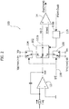
Figure 2 . - In
Figure 2 parts or elements like parts or elements already discussed in connection with theFigure 1 are indicated with like references. A corresponding description will not be repeated here for brevity. - The circuit of
Figure 2 is thus again configured for receiving, at one (e.g. inverting) input of thecomparator 14, the modulating signal Vmod and producing (in a manner known per se) a PWM modulated signal Out(PWM) by comparing the modulating signal Vmod with a carrier signal Vtri2. Such a carrier signal may again be produced starting from a square wave input (e.g. current) signal Isq having rising and falling edges and by producing from the square (rectangular) wave input signal Isq (e.g. via integration at the integrator 12) a triangular wave (e.g. voltage) signal Vtri comprising alternating peaks and valleys. - In one or more embodiments as exemplified in
Figure 2 , the signal Vtri can be applied to a circuit portion indicated 100 (to be discussed in the following), active between the circuit block 12 (integrator) and the circuit block 14 (comparator) to generate the carrier signal Vtri2 from the triangular wave signal Vtri. - As discussed in the following, the
circuit portion 100 is configured for, so-to-say, modifying the signal Vtri by forcing the peaks and valleys of the signal to certain upper and lower reference values, with such modifying/forcing being adapted to be effected selectively (as a result of the occurrence of certain conditions), with the further optional capability for thecircuit portion 100 to select a first forcing mode (pulse skipping optimization) and a second forcing mode (pulse skipping inhibit), wherein a first and a second value can be chosen for the upper and lower reference values, respectively. - By comparing the circuit of
Figure 2 with the circuit ofFigure 1 one may note that the pulse generator Ipulse at the input of theintegrator 12 is no longer present in the circuit ofFigure 2 . - In one or more embodiments, in the circuit of
Figure 2 , the function of providing (e.g. voltage) pulses at the vertexes (peaks and valleys) of the waveform Vtri is implemented by means of aswitch 102 in thecircuit portion 100. - In one or more embodiments as exemplified herein, the
switch 102 comprises anoutput node 102a coupled to the input of thecomparator 14 to provide the signal Vtri2 as a signal selected out of three possible options applied to three inputs to theswitch 102, these inputs being labeled "0", "1" and "2", respectively. - The input "0" corresponds to the output from the
integrator 12, that is the triangular waveform signal Vtri. - The input "1" is obtained from a
circuit block 104 which in turn comprises a switch which may selectively coupled, over a certain forcing time interval, to either one of two "higher" reference (e.g. DC voltage) levels Vp and Vp(max)+dv. - The input "2" is obtained from a
circuit block 106 which in term comprises a switch which may selectively coupled, over a certain forcing time interval, to either one of two "lower" reference (e.g. DC voltage) levels Vm and Vm(max)-dv. - These reference levels may be obtained from conventional signal (e.g. voltage) sources, not visible in the figures.
- As discussed in the following, these reference levels may be regarded as corresponding to some sort of upper and lower "end of scale" reference values to which the input triangular signal Vtri may be forced upward (to Vp or, alternatively, Vp(max)+dv) or downward (to Vm or, alternatively, Vm(max)-dv), over a certain forcing time interval (that is, not merely as instantaneous pulses) in order to provide pulse skipping control/pulse skipping inhibit functions.
- As exemplified in
Figure 2 , the circuit blocks 104, 106 operate under the control of a pulse skipping inhibit/enabled signal I/E (operation mode selection) obtained over aline 108 from a source (not visible in the figures), according to principles known per se (see alsoUS 9 595 946 B2 -
Reference 110 inFigure 2 indicates a timing generator which receives the PWM clock signal (e.g. Isq, generated in any conventional manner) over aline 110a, e.g. with a 50% duty cycle. - In one or more embodiments as exemplified in the time diagrams of
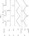
Figure 3 , theswitch 102 may be controlled by thetiming generator 110 based on three clocking signals, comprising: - the clock signal (PWM clock), e.g. with a duty cycle = 50%, having rising edges RE and falling edges FE: see the diagram a) in
Figure 3 ; - a first square wave (pulse)
signal Sync 1 which goes to a logic level "1", at the rising edges RE of the clock signal for a certain time duration (e.g. centered temporarily on the rising edges RE) which may be selected to correspond to a smallest desired duty cycle value for the output signal: see the diagram b) inFigure 3 ; and - a second square wave (pulse)
signal Sync 2 which goes to a logic level "1" at the falling edges FE of the clock signal for a time duration (e.g. centered temporarily on the falling edges FE) which again may be selected to correspond to the smallest desired duty cycle value for the output signal: see the diagram c) inFigure 3 . - By observing the diagrams in portions b) and c) in
Figure 3 one may note that the square wave signals Sync1 andSync 2 comprise pulses of a certain time duration (and not merely instantaneous spike-like pulses) with that time duration possibly dictated by a smallest desired duty cycle value for the PWM modulated output signal Out(PWM), e.g. selected equal to the pulse width (pulse active time) or "on" time (PW, in the formula reproduced in the introductory portion of this description) corresponding to a smallest desired duty cycle value for Out(PWM). - Portions d) and e) of
Figure 3 are exemplary of a corresponding possible time behavior of Vtri and Vtri2. - In one or more embodiments, the
switch 102 may thus take: - the "0" position (carrier transfer setting), with Vtri applied to the
comparator 14 as Vtri2, as a result of both signals Sync1 and Sync2 being equal to zero, namely with Sync1 = Sync2 = 0; - the "1" position (first carrier forcing setting), as a result of Sync1 = 1 and
Sync 2 = 0, so that the output from theblock 104 is coupled to thecomparator 14, with Vtri2 resulting from Vtri being forced "upward" to either one of the upper reference values Vp or Vp(max)+dv (e.g. DC voltages) as a function of the position taken by the switch in theblock 104; - the "2" position (second carrier forcing setting), as a result of Sync1 = 0 and
Sync 2 = 1, so that the output from theblock 106 is coupled to thecomparator 14, with Vtri2 resulting from Vtri being forced "downward" to either one of the lower reference values Vm or Vm(max)-dv (e.g. DC voltages) as a function of the position taken by the switch in theblock 106. - As exemplified in portions d) and e) of
Figure 3 , while corresponding to Vtri when Sync1 = Sync2 = 0, as a result of Sync1 or Sync2 going to 1, the signal Vtri2 will be "modified" with respect to triangular signal Vtri input to thecircuit portion 100 insofar as the vertexes (peaks and valleys) of Vtri will have superposed pulses (upward and downward, respectively) of controlled shape and amplitude over the duration of the forcing time intervals set by Sync1 orSync 2. - The modified triangular-with-superposed-pulses waveform of Vtri2 resulting from selectively forcing the alternating peaks and valleys of the triangular wave carrier signal to upper and lower reference values will thus exhibit (as a function of the value of pulse skipping optimization/inhibit signal I/E on the line 108) :
- with the
switches - with the
switches - In one or more embodiments, the first reference values Vp and Vm, may be selected to be within the largest expected swing of the modulating signal Vmod, that is smaller (in modulus) of the highest and lowest expected values for Vmod.
- In one or more embodiments, this first option will result in a first forcing mode to produce in Vtri2 upper and lower reference values selected at first values Vp, Vm lying within the modulating signal swing between highest and lowest values.
- In that way, the area near saturation of the PWM signal will be made (more) regular, especially in systems with feedback, reducing the gain of the PWM modulator in that zone.
- In fact, with Vmod reaching values in excess of Vp or lower than Vm the duty cycle will reach
corresponding values 100% or 0%, thus achieving a large output signal dynamics, and performing a pulse skipping optimization function. - In one or more embodiments, in addition to being larger (in modulus) of both Vp and Vm, the second reference values Vp(max)+dv and Vm(max)-dv may be selected to be in excess of the largest expected swing of the modulating signal Vmod, that is larger (in modulus) of the highest and lowest expected values for Vmod.
- In one or more embodiments, this second option will result in a second forcing mode to produce in Vtri2 upper and lower reference values selected at second values (Vp(max)+dv, Vm(max)-dv) lying outside the modulating signal swing between highest and lowest values.
- These may serve the purpose of avoiding that the duty cycle may reach values such as 100% or 0%, thereby maintaining the nominal clock frequency with a lowest duty cycle value as set by the duty cycle of the signals Sync1 and Sync2, thus performing a pulse skipping inhibit function.
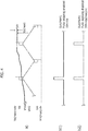
- This type of operation is exemplified in
Figure 4 wherein portion a) shows a possible behavior of the signal Vtri2 with a possible time behavior of the modulating signal Vmod also shown for direct reference. - The portions b1) and b2) of
Figure 4 show a possible time behavior of the PWM modulated output signal Out (PWM) : - with pulse skipping enabled and optimized (with the
switch 104 switched on Vp), and - with pulse skipping disabled/inhibited, with the
switch 104 switched on Vp(max)+dv. - A similar result will be provided with the
switch 106 on Vm and Vm(max)-dv (by taking into account the possible reversed polarity). - The block diagram of
Figure 5 is exemplary of the possible inclusion of a circuit as exemplified inFigure 2 in a high-frequency PWM power circuit (e.g. a class D audio amplifier) receiving an input signal Vin and comprising aninput integrator 200 and wherein the output signal Out(PWM) from thecomparator 14 is fed to apower switch 202 switching between two values +Vpot and -Vpot. The diagram ofFigure 5 also shows a (negative)feedback path 206 withgain 1/K to be subtracted at aninput node 208 from the input signal Vin input to theintegrator 200. The output from theswitch 202 can be applied to an output LC (reconstruction)filter 204 to provide an output amplified signal KVin (that is the input signal Vin having a gain K applied thereto). - As for the rest, operation of an arrangement as exemplified in
Figure 5 (essentially a class D amplifier) is otherwise conventional in the art, thus making it unnecessary to provide a more detailed description herein. - In one or more embodiments, a circuit may comprise:
- a first circuit block (e.g. the integrator 12) configured for receiving a square wave input signal (e.g. Isq) having rising and falling edges (see e.g. RE and FE in
Figure 3a ) and producing from the square wave input signal (e.g. by integration) a triangular wave signal (e.g. Vtri, comprising alternating peaks and valleys), - a second circuit block (e.g. the comparator 14) configured for receiving a modulating signal (e.g. Vmod) and producing a PWM modulated signal (e.g. Out(PWM)) by comparing the modulating signal with a carrier signal (e.g. Vtri2),
- a switching circuit block (e.g. 100) between the first circuit block and the second circuit block, wherein the switching circuit block includes reference inputs (e.g. 104 and 106) configured for receiving reference signals having upper (e.g. Vp, Vp(max)+dv) and lower (e.g. Vm; Vm(max)-dv) reference values and is selectively (e.g. as function of Sync1, Sync2 and, possibly I/E) switchable (102) between:
- a carrier transfer setting (e.g. position 0 of the switch 102), wherein the switching circuit block couples the first circuit block to the second circuit block to transfer thereto the triangular wave signal as the carrier signal,
- at least one carrier forcing setting (
e.g. positions - In one or more embodiments:
- the second circuit block may be configured for receiving a modulating signal (e.g. Vmod) having a modulating signal swing between highest and lowest modulating signal values,
- the switching circuit block:
- i) includes reference inputs (e.g. 104 and 106) configured for receiving reference signals having first upper (e.g. Vp) and first lower (e.g. Vm) reference values lying within the modulating signal swing as well as second upper (e.g. Vp(max)+dv) and second lower (e.g. Vm(max)-dv) reference values lying outside the modulating signal swing,
- ii) is selectively switchable (e.g. at the level of
switches 104 and 106) between:
- a first carrier forcing setting (see e.g. signal E = enable on line 108), wherein the switching circuit block applies to the second circuit block said reference signals with said first upper and first lower reference values,
- a second carrier forcing setting (see e.g. signal I = inhibit or disable on line 108), wherein the switching circuit block applies to the second circuit block said reference signals with said second upper and second lower reference values.
- In one or more embodiments:
- the second circuit block may be configured for producing the PWM modulated signal with a lowest value for the PWM duty cycle wherein the PWM modulated signal has a lowest pulse active time at the selected lowest value for the duty cycle,
- the switching circuit block is selectively switchable to the at least one carrier forcing setting over carrier forcing intervals equal to said lowest pulse active time.
- One or more embodiments may comprise a clock circuit block (e.g. 110) sensitive to the rising and falling edges (RE, FE) of the square wave input signal, the clock circuit block may be configured for driving the switching circuit block to switch between the carrier transfer setting and the at least one carrier forcing setting at the rising and falling edges of the square wave input signal.
- In one or more embodiments, the clock circuit block may be configured for driving the switching circuit block to switch to the at least one carrier forcing setting over carrier forcing intervals centered around the rising and falling edges of the square wave input signal.
- A device according to one or more embodiments may comprise:
- a PWM modulation circuit (e.g. 12, 14, 100) according to one or more embodiments producing a PWM modulated signal,
- an input circuit block (e.g. 200, 208) configured for receiving an input signal (e.g. Vin) and providing to the PWM modulation circuit said modulating signal as a function of said input signal (Vin),
- a switching power stage (e.g. 202) driven by the PWM modulated signal from the PWM modulation circuit, and
- a low-pass filter circuit (e.g. 204) receiving a switching power signal from the switching power stage and producing therefrom an amplified replica (e.g. KVin) of the input signal.
- One or more embodiments may comprise a feedback path (e.g. 206) between the switching power stage and the input circuit block.
- In one or more embodiments, a method may comprise:
- receiving a modulating signal,
- producing a PWM modulated signal by comparing the modulating signal with a carrier signal, the carrier signal produced by receiving a square wave input signal having rising and falling edges and producing (e.g. via integration) from the square wave input signal a triangular wave signal (comprising alternating peaks and valleys),
- selectively forcing the (alternating peaks and valleys of the) carrier signal to upper and lower reference values, respectively, over carrier forcing intervals (see e.g. the duration of the pulses of Sync1 and Sync2 in
Figure 3 , parts b) and c) at the rising (e.g. RE) and falling edges (e.g FE) of the square wave input signal, the carrier forcing intervals optionally centered around the rising and falling edges of the square wave input signal. - In one or more embodiments, the modulating signal may have a modulating signal swing between highest and lowest modulating signal values, wherein selectively forcing the carrier signal to upper and lower reference values may comprise:
- a first carrier forcing mode wherein the upper and lower reference values are selected at first values (e.g. Vp, Vm) lying within the modulating signal swing, and
- a second carrier forcing mode wherein the upper and lower reference values are selected at second values (e.g. Vp(max)+dv, Vm(max)-dv) lying outside the modulating signal swing.
- One or more embodiments may comprise:
- selecting a lowest value for the duty cycle of the PWM modulated signal wherein the PWM modulated signal has a lowest pulse active time at the selected lowest value for the duty cycle,
- selecting the duration of the carrier forcing intervals to the upper and lower reference values equal to said lowest pulse active time.
- Without prejudice to the underlying principles, the details and embodiments may vary, even significantly, with respect to what has been described by way of example only without departing from the extent of protection. The extent of protection is defined by the annexed claims.
Claims (10)
- A circuit, comprising:- a first circuit block (12) configured for receiving a square wave input signal (Isq) having rising (RE) and falling (FE) edges and producing from the square wave input signal (Isq) a triangular wave signal (Vtri),- a second circuit block (14) configured for receiving a modulating signal (Vmod) and producing a PWM modulated signal (Out(PWM)) by comparing (14) the modulating signal (Vmod) with a carrier signal (Vtri2),- a switching circuit block (100) active between the first circuit block (12) and the second circuit block (14), wherein the switching circuit block (100) includes reference inputs (e.g. 104 and 106) configured for receiving reference signals having upper (e.g. Vp, Vp(max)+dv) and lower (e.g. Vm; Vm(max)-dv) reference values and is selectively (Sync1, Sync2; I/E) switchable (102) between:- a carrier transfer setting (0), wherein the switching circuit block (100) couples the first circuit block (12) to the second circuit block (14) to transfer thereto the triangular wave signal (Vtri) as the carrier signal (Vtri2),- at least one carrier forcing setting (1, 2) wherein the switching circuit block (100) applies to the second circuit block (14) said reference signals by forcing the carrier signal (Vtri2) to said upper (Vp, Vp(max)+dv) and lower (Vm; Vm(max)-dv) reference values, respectively.
- The circuit of claim 1, wherein:- the second circuit block (14) is configured for receiving a modulating signal (Vmod) having a modulating signal swing between highest and lowest modulating signal (Vmod) values,- the switching circuit block (100):i) includes reference inputs (e.g. 104 and 106) configured for receiving reference signals having first upper (Vp) and first lower (Vm) reference values lying within the modulating signal swing as well as second upper (Vp(max)+dv) and second lower (Vm(max)-dv) reference values lying outside the modulating signal swing,ii) is selectively switchable (104, 106) between:- a first carrier forcing setting (E), wherein the switching circuit block (100) applies to the second circuit block (14) said reference signals with said first upper (Vp) and first lower (Vm) reference values,- a second carrier forcing setting (I), wherein the switching circuit block (100) applies to the second circuit block (14) said reference signals with said second upper (Vp(max)+dv) and second lower (Vm(max)-dv) reference values.
- The circuit of claim 1 or claim 2, wherein:- the second circuit block (14) is configured for producing the PWM modulated signal (Out(PWM)) with a lowest value for the PWM duty cycle wherein the PWM modulated signal has a lowest pulse active time at the selected lowest value for the duty cycle,- the switching circuit block (100) is selectively (Sync1, Sync2) switchable (102) to the at least one carrier forcing setting (1, 2) over carrier forcing intervals equal to said lowest pulse active time.
- The circuit of any of the previous claims, comprising a clock circuit block (110) sensitive to the rising (RE) and falling (FE) edges of the square wave input signal (Isq), the clock circuit block (110) configured for driving the switching circuit block (100) to switch between the carrier transfer setting (0) and the at least one carrier forcing setting (1, 2) at the rising (RE) and falling (FE) edges of the square wave input signal (Isq).
- The circuit of claim 4, wherein the clock circuit block (110) is configured for driving the switching circuit block (100) to switch to the at least one carrier forcing setting (1, 2) over carrier forcing intervals centered around the rising (RE) and falling (FE) edges of the square wave input signal (Isq).
- A device, comprising:- a PWM modulation circuit (12, 14, 100) according to any of claims 1 to 5 producing a PWM modulated signal (Out(PWM)),- an input circuit block (200, 208) configured for receiving an input signal (Vin) and providing to the PWM modulation circuit (12, 14, 100) said modulating signal (Vmod) as a function of said input signal (Vin),- a switching power stage (202) driven by the PWM modulated signal (Out(PWM)) from the PWM modulation circuit (12, 14, 100), and- a low-pass filter circuit (204) receiving a switching power signal from the switching power stage (202) and producing therefrom an amplified replica (KVin) of the input signal (Vin).
- The device of claim 6, comprising a feedback path (206) between the switching power stage (202) and the input circuit block (208).
- A method, comprising:- receiving (14) a modulating signal (Vmod),- producing a PWM modulated signal (Out(PWM)) by comparing (14) the modulating signal (Vmod) with a carrier signal (Vtri2), the carrier signal (Vtri2) produced by receiving a square wave input signal (Isq) having rising (RE) and falling (FE) edges and producing (12) from the square wave input signal (Isq) a triangular wave signal (Vtri),wherein the method comprises selectively (Sync1, Sync2) forcing the carrier signal (Vtri2) to upper (Vp, Vp(max)+dv) and lower (Vm; Vm(max)-dv) reference values, respectively, over carrier forcing intervals at the rising (RE) and falling edges (FE) of the square wave input signal (Isq), the carrier forcing intervals preferably centered around the rising (RE) and falling (FE) edges of the square wave input signal (Isq).
- The method of claim 8, wherein the modulating signal (Vmod) has a modulating signal swing between highest and lowest modulating signal (Vmod) values, wherein selectively (Sync1, Sync2) forcing the carrier signal (Vtri2) to upper and lower reference values comprises:- a first carrier forcing mode wherein the upper and lower reference values are selected at first values (Vp, Vm) lying within the modulating signal swing, and- a second carrier forcing mode wherein the upper and lower reference values are selected at second values (Vp(max)+dv, Vm(max)-dv) lying outside the modulating signal swing.
- The method of claim 8 or claim 9, comprising:- selecting a lowest value for the duty cycle of the PWM modulated signal (Out (PWM)) wherein the PWM modulated signal has a lowest pulse active time at the selected lowest value for the duty cycle,- selecting the duration of the carrier forcing intervals to the upper (Vp, Vp(max)+dv) and lower (Vm; Vm(max)-dv) reference values equal to said lowest pulse active time.
Applications Claiming Priority (1)
| Application Number | Priority Date | Filing Date | Title |
|---|---|---|---|
| IT102017000118558A IT201700118558A1 (en) | 2017-10-19 | 2017-10-19 | MODULATION CIRCUIT WITH IMPULSE WIDTH, CORRESPONDENT DEVICE AND PROCEDURE |
Publications (2)
| Publication Number | Publication Date |
|---|---|
| EP3474448A1 true EP3474448A1 (en) | 2019-04-24 |
| EP3474448B1 EP3474448B1 (en) | 2021-12-01 |
Family
ID=61148439
Family Applications (1)
| Application Number | Title | Priority Date | Filing Date |
|---|---|---|---|
| EP18199802.2A Active EP3474448B1 (en) | 2017-10-19 | 2018-10-11 | A pulse width modulation circuit, corresponding device and method |
Country Status (4)
| Country | Link |
|---|---|
| US (1) | US10560082B2 (en) |
| EP (1) | EP3474448B1 (en) |
| CN (2) | CN209120151U (en) |
| IT (1) | IT201700118558A1 (en) |
Families Citing this family (7)
| Publication number | Priority date | Publication date | Assignee | Title |
|---|---|---|---|---|
| IT201700118558A1 (en) * | 2017-10-19 | 2019-04-19 | St Microelectronics Srl | MODULATION CIRCUIT WITH IMPULSE WIDTH, CORRESPONDENT DEVICE AND PROCEDURE |
| CN110620570B (en) * | 2019-09-24 | 2022-03-08 | 中国工程物理研究院激光聚变研究中心 | Low-jitter pulse width high-resolution adjustable square wave pulse generation system and method |
| CN110958201A (en) * | 2019-12-31 | 2020-04-03 | 郑州航空工业管理学院 | Signal Transmission System for Applied Mathematics |
| IT202000014302A1 (en) | 2020-06-16 | 2021-12-16 | St Microelectronics Srl | CORRESPONDING MODULATOR CIRCUIT, DEVICE AND PROCEDURE |
| US11463052B2 (en) | 2020-11-30 | 2022-10-04 | Stmicroelectronics S.R.L. | PWM driving circuit and method |
| TWI857863B (en) * | 2023-11-21 | 2024-10-01 | 立錡科技股份有限公司 | Class d amplifier capable of anti-clipping |
| CN118508932B (en) * | 2024-05-23 | 2025-08-22 | 惠科股份有限公司 | Linkage circuit, clock signal duty cycle adjustment method and display panel |
Citations (5)
| Publication number | Priority date | Publication date | Assignee | Title |
|---|---|---|---|---|
| US5291562A (en) * | 1990-01-22 | 1994-03-01 | Fuji Photo Film Co., Ltd. | Image signal processing apparatus producing a narrowed pulse width modulated signal using an asymmetrically centered triangle reference waveform |
| EP1657815A1 (en) * | 2004-11-12 | 2006-05-17 | Dialog Semiconductor GmbH | Frequency stabilization technique for self oscillating modulator |
| US20070018697A1 (en) * | 2005-07-25 | 2007-01-25 | Logah Technology Corp. | Double frequency signal generator |
| US20070024365A1 (en) * | 2005-07-29 | 2007-02-01 | Texas Instruments, Inc. | Class-D amplifier system |
| WO2009001254A2 (en) * | 2007-06-27 | 2008-12-31 | Nxp B.V. | Pulse width modulation circuit and class-d amplifier comprising the pwm circuit |
Family Cites Families (5)
| Publication number | Priority date | Publication date | Assignee | Title |
|---|---|---|---|---|
| US8022756B2 (en) * | 2007-05-15 | 2011-09-20 | Qualcomm, Incorporated | Output circuits with class D amplifier |
| US9595946B2 (en) * | 2014-01-17 | 2017-03-14 | Stmicroelectronics S.R.L. | PWM modulator |
| KR101906817B1 (en) * | 2014-10-24 | 2018-10-11 | 씨러스 로직 인코포레이티드 | Amplifier with adjustable ramp up/down gain for minimizing or eliminating pop noise |
| US10180448B2 (en) * | 2015-05-15 | 2019-01-15 | Analog Devices, Inc. | Circuit and method for pulse width modulation |
| IT201700118558A1 (en) * | 2017-10-19 | 2019-04-19 | St Microelectronics Srl | MODULATION CIRCUIT WITH IMPULSE WIDTH, CORRESPONDENT DEVICE AND PROCEDURE |
-
2017
- 2017-10-19 IT IT102017000118558A patent/IT201700118558A1/en unknown
-
2018
- 2018-10-04 US US16/151,380 patent/US10560082B2/en active Active
- 2018-10-11 EP EP18199802.2A patent/EP3474448B1/en active Active
- 2018-10-18 CN CN201821693203.3U patent/CN209120151U/en not_active Withdrawn - After Issue
- 2018-10-18 CN CN201811217392.1A patent/CN109687853B/en active Active
Patent Citations (5)
| Publication number | Priority date | Publication date | Assignee | Title |
|---|---|---|---|---|
| US5291562A (en) * | 1990-01-22 | 1994-03-01 | Fuji Photo Film Co., Ltd. | Image signal processing apparatus producing a narrowed pulse width modulated signal using an asymmetrically centered triangle reference waveform |
| EP1657815A1 (en) * | 2004-11-12 | 2006-05-17 | Dialog Semiconductor GmbH | Frequency stabilization technique for self oscillating modulator |
| US20070018697A1 (en) * | 2005-07-25 | 2007-01-25 | Logah Technology Corp. | Double frequency signal generator |
| US20070024365A1 (en) * | 2005-07-29 | 2007-02-01 | Texas Instruments, Inc. | Class-D amplifier system |
| WO2009001254A2 (en) * | 2007-06-27 | 2008-12-31 | Nxp B.V. | Pulse width modulation circuit and class-d amplifier comprising the pwm circuit |
Also Published As
| Publication number | Publication date |
|---|---|
| EP3474448B1 (en) | 2021-12-01 |
| CN109687853B (en) | 2023-07-14 |
| CN209120151U (en) | 2019-07-16 |
| US20190123731A1 (en) | 2019-04-25 |
| US10560082B2 (en) | 2020-02-11 |
| CN109687853A (en) | 2019-04-26 |
| IT201700118558A1 (en) | 2019-04-19 |
Similar Documents
| Publication | Publication Date | Title |
|---|---|---|
| EP3474448B1 (en) | A pulse width modulation circuit, corresponding device and method | |
| US20040232978A1 (en) | Filterless class D amplifiers using spread spectrum PWM modulation | |
| US6847257B2 (en) | Efficient minimum pulse spread spectrum modulation for filterless class D amplifiers | |
| EP0503571B1 (en) | Pulse-width modulation amplifier | |
| US7348840B2 (en) | Feedback controller for PWM amplifier | |
| US9231535B2 (en) | Silent start class-D amplifier | |
| US8022757B2 (en) | Class D power amplifier | |
| US8154358B2 (en) | System and method of changing a PWM power spectrum | |
| JP2010504004A (en) | Class D audio amplifier | |
| US8659351B2 (en) | Electronic circuit for driving a switching amplifier | |
| EP2332251B1 (en) | Pulse-width modulation with selective pulse-elimination | |
| US7545207B2 (en) | Control circuit and method for a switching amplifier | |
| JP2021521659A (en) | Class D amplifier with duty cycle control | |
| US11750163B2 (en) | Deglitching circuit and method in a class-D amplifier | |
| US9991852B2 (en) | System and method for close-down pop reduction | |
| US7388426B2 (en) | Control circuit and method for a switching amplifier | |
| EP4007166B1 (en) | Pwm driving circuit and method | |
| US7279966B2 (en) | Systems for pseudo-BD modulation | |
| EP2562933A1 (en) | Class D amplifier and control method | |
| EP3926829A1 (en) | Modulator circuit, corresponding device and method | |
| US12323112B1 (en) | Signal amplifier | |
| JP2009284413A (en) | Digital power amplifier | |
| JP2005328196A (en) | Overmodulation preventing circuit in pwm modulation | |
| KR101349002B1 (en) | Amplification circuit and method therefor |
Legal Events
| Date | Code | Title | Description |
|---|---|---|---|
| PUAI | Public reference made under article 153(3) epc to a published international application that has entered the european phase |
Free format text: ORIGINAL CODE: 0009012 |
|
| STAA | Information on the status of an ep patent application or granted ep patent |
Free format text: STATUS: THE APPLICATION HAS BEEN PUBLISHED |
|
| AK | Designated contracting states |
Kind code of ref document: A1 Designated state(s): AL AT BE BG CH CY CZ DE DK EE ES FI FR GB GR HR HU IE IS IT LI LT LU LV MC MK MT NL NO PL PT RO RS SE SI SK SM TR |
|
| AX | Request for extension of the european patent |
Extension state: BA ME |
|
| STAA | Information on the status of an ep patent application or granted ep patent |
Free format text: STATUS: REQUEST FOR EXAMINATION WAS MADE |
|
| 17P | Request for examination filed |
Effective date: 20191001 |
|
| RBV | Designated contracting states (corrected) |
Designated state(s): AL AT BE BG CH CY CZ DE DK EE ES FI FR GB GR HR HU IE IS IT LI LT LU LV MC MK MT NL NO PL PT RO RS SE SI SK SM TR |
|
| REG | Reference to a national code |
Ref country code: DE Ref legal event code: R079 Ref document number: 602018027407 Country of ref document: DE Free format text: PREVIOUS MAIN CLASS: H03K0007080000 Ipc: H03K0005125200 |
|
| RIC1 | Information provided on ipc code assigned before grant |
Ipc: H03K 5/1252 20060101AFI20210420BHEP Ipc: H03K 7/08 20060101ALI20210420BHEP |
|
| RIN1 | Information on inventor provided before grant (corrected) |
Inventor name: BOTTI, EDOARDO Inventor name: GALLO, NOEMI |
|
| GRAP | Despatch of communication of intention to grant a patent |
Free format text: ORIGINAL CODE: EPIDOSNIGR1 |
|
| STAA | Information on the status of an ep patent application or granted ep patent |
Free format text: STATUS: GRANT OF PATENT IS INTENDED |
|
| INTG | Intention to grant announced |
Effective date: 20210705 |
|
| GRAS | Grant fee paid |
Free format text: ORIGINAL CODE: EPIDOSNIGR3 |
|
| GRAA | (expected) grant |
Free format text: ORIGINAL CODE: 0009210 |
|
| STAA | Information on the status of an ep patent application or granted ep patent |
Free format text: STATUS: THE PATENT HAS BEEN GRANTED |
|
| AK | Designated contracting states |
Kind code of ref document: B1 Designated state(s): AL AT BE BG CH CY CZ DE DK EE ES FI FR GB GR HR HU IE IS IT LI LT LU LV MC MK MT NL NO PL PT RO RS SE SI SK SM TR |
|
| REG | Reference to a national code |
Ref country code: GB Ref legal event code: FG4D |
|
| REG | Reference to a national code |
Ref country code: AT Ref legal event code: REF Ref document number: 1452749 Country of ref document: AT Kind code of ref document: T Effective date: 20211215 Ref country code: CH Ref legal event code: EP |
|
| REG | Reference to a national code |
Ref country code: IE Ref legal event code: FG4D |
|
| REG | Reference to a national code |
Ref country code: DE Ref legal event code: R096 Ref document number: 602018027407 Country of ref document: DE |
|
| REG | Reference to a national code |
Ref country code: LT Ref legal event code: MG9D |
|
| REG | Reference to a national code |
Ref country code: NL Ref legal event code: MP Effective date: 20211201 |
|
| REG | Reference to a national code |
Ref country code: AT Ref legal event code: MK05 Ref document number: 1452749 Country of ref document: AT Kind code of ref document: T Effective date: 20211201 |
|
| PG25 | Lapsed in a contracting state [announced via postgrant information from national office to epo] |
Ref country code: RS Free format text: LAPSE BECAUSE OF FAILURE TO SUBMIT A TRANSLATION OF THE DESCRIPTION OR TO PAY THE FEE WITHIN THE PRESCRIBED TIME-LIMIT Effective date: 20211201 Ref country code: LT Free format text: LAPSE BECAUSE OF FAILURE TO SUBMIT A TRANSLATION OF THE DESCRIPTION OR TO PAY THE FEE WITHIN THE PRESCRIBED TIME-LIMIT Effective date: 20211201 Ref country code: FI Free format text: LAPSE BECAUSE OF FAILURE TO SUBMIT A TRANSLATION OF THE DESCRIPTION OR TO PAY THE FEE WITHIN THE PRESCRIBED TIME-LIMIT Effective date: 20211201 Ref country code: BG Free format text: LAPSE BECAUSE OF FAILURE TO SUBMIT A TRANSLATION OF THE DESCRIPTION OR TO PAY THE FEE WITHIN THE PRESCRIBED TIME-LIMIT Effective date: 20220301 Ref country code: AT Free format text: LAPSE BECAUSE OF FAILURE TO SUBMIT A TRANSLATION OF THE DESCRIPTION OR TO PAY THE FEE WITHIN THE PRESCRIBED TIME-LIMIT Effective date: 20211201 |
|
| PG25 | Lapsed in a contracting state [announced via postgrant information from national office to epo] |
Ref country code: SE Free format text: LAPSE BECAUSE OF FAILURE TO SUBMIT A TRANSLATION OF THE DESCRIPTION OR TO PAY THE FEE WITHIN THE PRESCRIBED TIME-LIMIT Effective date: 20211201 Ref country code: PL Free format text: LAPSE BECAUSE OF FAILURE TO SUBMIT A TRANSLATION OF THE DESCRIPTION OR TO PAY THE FEE WITHIN THE PRESCRIBED TIME-LIMIT Effective date: 20211201 Ref country code: NO Free format text: LAPSE BECAUSE OF FAILURE TO SUBMIT A TRANSLATION OF THE DESCRIPTION OR TO PAY THE FEE WITHIN THE PRESCRIBED TIME-LIMIT Effective date: 20220301 Ref country code: LV Free format text: LAPSE BECAUSE OF FAILURE TO SUBMIT A TRANSLATION OF THE DESCRIPTION OR TO PAY THE FEE WITHIN THE PRESCRIBED TIME-LIMIT Effective date: 20211201 Ref country code: HR Free format text: LAPSE BECAUSE OF FAILURE TO SUBMIT A TRANSLATION OF THE DESCRIPTION OR TO PAY THE FEE WITHIN THE PRESCRIBED TIME-LIMIT Effective date: 20211201 Ref country code: GR Free format text: LAPSE BECAUSE OF FAILURE TO SUBMIT A TRANSLATION OF THE DESCRIPTION OR TO PAY THE FEE WITHIN THE PRESCRIBED TIME-LIMIT Effective date: 20220302 Ref country code: ES Free format text: LAPSE BECAUSE OF FAILURE TO SUBMIT A TRANSLATION OF THE DESCRIPTION OR TO PAY THE FEE WITHIN THE PRESCRIBED TIME-LIMIT Effective date: 20211201 |
|
| PG25 | Lapsed in a contracting state [announced via postgrant information from national office to epo] |
Ref country code: NL Free format text: LAPSE BECAUSE OF FAILURE TO SUBMIT A TRANSLATION OF THE DESCRIPTION OR TO PAY THE FEE WITHIN THE PRESCRIBED TIME-LIMIT Effective date: 20211201 |
|
| PG25 | Lapsed in a contracting state [announced via postgrant information from national office to epo] |
Ref country code: SM Free format text: LAPSE BECAUSE OF FAILURE TO SUBMIT A TRANSLATION OF THE DESCRIPTION OR TO PAY THE FEE WITHIN THE PRESCRIBED TIME-LIMIT Effective date: 20211201 Ref country code: SK Free format text: LAPSE BECAUSE OF FAILURE TO SUBMIT A TRANSLATION OF THE DESCRIPTION OR TO PAY THE FEE WITHIN THE PRESCRIBED TIME-LIMIT Effective date: 20211201 Ref country code: RO Free format text: LAPSE BECAUSE OF FAILURE TO SUBMIT A TRANSLATION OF THE DESCRIPTION OR TO PAY THE FEE WITHIN THE PRESCRIBED TIME-LIMIT Effective date: 20211201 Ref country code: PT Free format text: LAPSE BECAUSE OF FAILURE TO SUBMIT A TRANSLATION OF THE DESCRIPTION OR TO PAY THE FEE WITHIN THE PRESCRIBED TIME-LIMIT Effective date: 20220401 Ref country code: EE Free format text: LAPSE BECAUSE OF FAILURE TO SUBMIT A TRANSLATION OF THE DESCRIPTION OR TO PAY THE FEE WITHIN THE PRESCRIBED TIME-LIMIT Effective date: 20211201 Ref country code: CZ Free format text: LAPSE BECAUSE OF FAILURE TO SUBMIT A TRANSLATION OF THE DESCRIPTION OR TO PAY THE FEE WITHIN THE PRESCRIBED TIME-LIMIT Effective date: 20211201 |
|
| REG | Reference to a national code |
Ref country code: DE Ref legal event code: R097 Ref document number: 602018027407 Country of ref document: DE |
|
| PG25 | Lapsed in a contracting state [announced via postgrant information from national office to epo] |
Ref country code: IS Free format text: LAPSE BECAUSE OF FAILURE TO SUBMIT A TRANSLATION OF THE DESCRIPTION OR TO PAY THE FEE WITHIN THE PRESCRIBED TIME-LIMIT Effective date: 20220401 |
|
| PLBE | No opposition filed within time limit |
Free format text: ORIGINAL CODE: 0009261 |
|
| STAA | Information on the status of an ep patent application or granted ep patent |
Free format text: STATUS: NO OPPOSITION FILED WITHIN TIME LIMIT |
|
| PG25 | Lapsed in a contracting state [announced via postgrant information from national office to epo] |
Ref country code: DK Free format text: LAPSE BECAUSE OF FAILURE TO SUBMIT A TRANSLATION OF THE DESCRIPTION OR TO PAY THE FEE WITHIN THE PRESCRIBED TIME-LIMIT Effective date: 20211201 Ref country code: AL Free format text: LAPSE BECAUSE OF FAILURE TO SUBMIT A TRANSLATION OF THE DESCRIPTION OR TO PAY THE FEE WITHIN THE PRESCRIBED TIME-LIMIT Effective date: 20211201 |
|
| 26N | No opposition filed |
Effective date: 20220902 |
|
| PG25 | Lapsed in a contracting state [announced via postgrant information from national office to epo] |
Ref country code: SI Free format text: LAPSE BECAUSE OF FAILURE TO SUBMIT A TRANSLATION OF THE DESCRIPTION OR TO PAY THE FEE WITHIN THE PRESCRIBED TIME-LIMIT Effective date: 20211201 |
|
| PG25 | Lapsed in a contracting state [announced via postgrant information from national office to epo] |
Ref country code: MC Free format text: LAPSE BECAUSE OF FAILURE TO SUBMIT A TRANSLATION OF THE DESCRIPTION OR TO PAY THE FEE WITHIN THE PRESCRIBED TIME-LIMIT Effective date: 20211201 Ref country code: IT Free format text: LAPSE BECAUSE OF FAILURE TO SUBMIT A TRANSLATION OF THE DESCRIPTION OR TO PAY THE FEE WITHIN THE PRESCRIBED TIME-LIMIT Effective date: 20211201 |
|
| REG | Reference to a national code |
Ref country code: CH Ref legal event code: PL |
|
| REG | Reference to a national code |
Ref country code: BE Ref legal event code: MM Effective date: 20221031 |
|
| GBPC | Gb: european patent ceased through non-payment of renewal fee |
Effective date: 20221011 |
|
| PG25 | Lapsed in a contracting state [announced via postgrant information from national office to epo] |
Ref country code: LU Free format text: LAPSE BECAUSE OF NON-PAYMENT OF DUE FEES Effective date: 20221011 |
|
| PG25 | Lapsed in a contracting state [announced via postgrant information from national office to epo] |
Ref country code: LI Free format text: LAPSE BECAUSE OF NON-PAYMENT OF DUE FEES Effective date: 20221031 Ref country code: FR Free format text: LAPSE BECAUSE OF NON-PAYMENT OF DUE FEES Effective date: 20221031 Ref country code: CH Free format text: LAPSE BECAUSE OF NON-PAYMENT OF DUE FEES Effective date: 20221031 |
|
| PG25 | Lapsed in a contracting state [announced via postgrant information from national office to epo] |
Ref country code: BE Free format text: LAPSE BECAUSE OF NON-PAYMENT OF DUE FEES Effective date: 20221031 |
|
| PG25 | Lapsed in a contracting state [announced via postgrant information from national office to epo] |
Ref country code: IE Free format text: LAPSE BECAUSE OF NON-PAYMENT OF DUE FEES Effective date: 20221011 Ref country code: GB Free format text: LAPSE BECAUSE OF NON-PAYMENT OF DUE FEES Effective date: 20221011 |
|
| PG25 | Lapsed in a contracting state [announced via postgrant information from national office to epo] |
Ref country code: HU Free format text: LAPSE BECAUSE OF FAILURE TO SUBMIT A TRANSLATION OF THE DESCRIPTION OR TO PAY THE FEE WITHIN THE PRESCRIBED TIME-LIMIT; INVALID AB INITIO Effective date: 20181011 |
|
| PG25 | Lapsed in a contracting state [announced via postgrant information from national office to epo] |
Ref country code: CY Free format text: LAPSE BECAUSE OF FAILURE TO SUBMIT A TRANSLATION OF THE DESCRIPTION OR TO PAY THE FEE WITHIN THE PRESCRIBED TIME-LIMIT Effective date: 20211201 |
|
| PG25 | Lapsed in a contracting state [announced via postgrant information from national office to epo] |
Ref country code: MK Free format text: LAPSE BECAUSE OF FAILURE TO SUBMIT A TRANSLATION OF THE DESCRIPTION OR TO PAY THE FEE WITHIN THE PRESCRIBED TIME-LIMIT Effective date: 20211201 |
|
| PG25 | Lapsed in a contracting state [announced via postgrant information from national office to epo] |
Ref country code: TR Free format text: LAPSE BECAUSE OF FAILURE TO SUBMIT A TRANSLATION OF THE DESCRIPTION OR TO PAY THE FEE WITHIN THE PRESCRIBED TIME-LIMIT Effective date: 20211201 |
|
| PG25 | Lapsed in a contracting state [announced via postgrant information from national office to epo] |
Ref country code: MT Free format text: LAPSE BECAUSE OF FAILURE TO SUBMIT A TRANSLATION OF THE DESCRIPTION OR TO PAY THE FEE WITHIN THE PRESCRIBED TIME-LIMIT Effective date: 20211201 |
|
| PGFP | Annual fee paid to national office [announced via postgrant information from national office to epo] |
Ref country code: DE Payment date: 20250923 Year of fee payment: 8 |