EP3471518A1 - Verfahren zur herstellung von optoelektronischen sensoren, insbesondere von miniatursensoren - Google Patents
Verfahren zur herstellung von optoelektronischen sensoren, insbesondere von miniatursensoren Download PDFInfo
- Publication number
- EP3471518A1 EP3471518A1 EP18194292.1A EP18194292A EP3471518A1 EP 3471518 A1 EP3471518 A1 EP 3471518A1 EP 18194292 A EP18194292 A EP 18194292A EP 3471518 A1 EP3471518 A1 EP 3471518A1
- Authority
- EP
- European Patent Office
- Prior art keywords
- printed circuit
- circuit board
- sensors
- plate
- sensor
- Prior art date
- Legal status (The legal status is an assumption and is not a legal conclusion. Google has not performed a legal analysis and makes no representation as to the accuracy of the status listed.)
- Granted
Links
Images


Classifications
-
- H—ELECTRICITY
- H05—ELECTRIC TECHNIQUES NOT OTHERWISE PROVIDED FOR
- H05K—PRINTED CIRCUITS; CASINGS OR CONSTRUCTIONAL DETAILS OF ELECTRIC APPARATUS; MANUFACTURE OF ASSEMBLAGES OF ELECTRICAL COMPONENTS
- H05K3/00—Apparatus or processes for manufacturing printed circuits
- H05K3/0097—Processing two or more printed circuits simultaneously, e.g. made from a common substrate, or temporarily stacked circuit boards
-
- H—ELECTRICITY
- H05—ELECTRIC TECHNIQUES NOT OTHERWISE PROVIDED FOR
- H05K—PRINTED CIRCUITS; CASINGS OR CONSTRUCTIONAL DETAILS OF ELECTRIC APPARATUS; MANUFACTURE OF ASSEMBLAGES OF ELECTRICAL COMPONENTS
- H05K3/00—Apparatus or processes for manufacturing printed circuits
- H05K3/0011—Working of insulating substrates or insulating layers
- H05K3/0044—Mechanical working of the substrate, e.g. drilling or punching
- H05K3/0052—Depaneling, i.e. dividing a panel into circuit boards; Working of the edges of circuit boards
-
- H—ELECTRICITY
- H05—ELECTRIC TECHNIQUES NOT OTHERWISE PROVIDED FOR
- H05K—PRINTED CIRCUITS; CASINGS OR CONSTRUCTIONAL DETAILS OF ELECTRIC APPARATUS; MANUFACTURE OF ASSEMBLAGES OF ELECTRICAL COMPONENTS
- H05K3/00—Apparatus or processes for manufacturing printed circuits
- H05K3/22—Secondary treatment of printed circuits
- H05K3/28—Applying non-metallic protective coatings
- H05K3/284—Applying non-metallic protective coatings for encapsulating mounted components
-
- H—ELECTRICITY
- H10—SEMICONDUCTOR DEVICES; ELECTRIC SOLID-STATE DEVICES NOT OTHERWISE PROVIDED FOR
- H10F—INORGANIC SEMICONDUCTOR DEVICES SENSITIVE TO INFRARED RADIATION, LIGHT, ELECTROMAGNETIC RADIATION OF SHORTER WAVELENGTH OR CORPUSCULAR RADIATION
- H10F55/00—Radiation-sensitive semiconductor devices covered by groups H10F10/00, H10F19/00 or H10F30/00 being structurally associated with electric light sources and electrically or optically coupled thereto
- H10F55/20—Radiation-sensitive semiconductor devices covered by groups H10F10/00, H10F19/00 or H10F30/00 being structurally associated with electric light sources and electrically or optically coupled thereto wherein the electric light source controls the radiation-sensitive semiconductor devices, e.g. optocouplers
- H10F55/25—Radiation-sensitive semiconductor devices covered by groups H10F10/00, H10F19/00 or H10F30/00 being structurally associated with electric light sources and electrically or optically coupled thereto wherein the electric light source controls the radiation-sensitive semiconductor devices, e.g. optocouplers wherein the radiation-sensitive devices and the electric light source are all semiconductor devices
-
- H—ELECTRICITY
- H10—SEMICONDUCTOR DEVICES; ELECTRIC SOLID-STATE DEVICES NOT OTHERWISE PROVIDED FOR
- H10F—INORGANIC SEMICONDUCTOR DEVICES SENSITIVE TO INFRARED RADIATION, LIGHT, ELECTROMAGNETIC RADIATION OF SHORTER WAVELENGTH OR CORPUSCULAR RADIATION
- H10F77/00—Constructional details of devices covered by this subclass
- H10F77/50—Encapsulations or containers
-
- H—ELECTRICITY
- H10—SEMICONDUCTOR DEVICES; ELECTRIC SOLID-STATE DEVICES NOT OTHERWISE PROVIDED FOR
- H10W—GENERIC PACKAGES, INTERCONNECTIONS, CONNECTORS OR OTHER CONSTRUCTIONAL DETAILS OF DEVICES COVERED BY CLASS H10
- H10W74/00—Encapsulations, e.g. protective coatings
- H10W74/01—Manufacture or treatment
- H10W74/014—Manufacture or treatment using batch processing
-
- H—ELECTRICITY
- H10—SEMICONDUCTOR DEVICES; ELECTRIC SOLID-STATE DEVICES NOT OTHERWISE PROVIDED FOR
- H10W—GENERIC PACKAGES, INTERCONNECTIONS, CONNECTORS OR OTHER CONSTRUCTIONAL DETAILS OF DEVICES COVERED BY CLASS H10
- H10W74/00—Encapsulations, e.g. protective coatings
- H10W74/10—Encapsulations, e.g. protective coatings characterised by their shape or disposition
- H10W74/111—Encapsulations, e.g. protective coatings characterised by their shape or disposition the semiconductor body being completely enclosed
- H10W74/114—Encapsulations, e.g. protective coatings characterised by their shape or disposition the semiconductor body being completely enclosed by a substrate and the encapsulations
-
- B—PERFORMING OPERATIONS; TRANSPORTING
- B29—WORKING OF PLASTICS; WORKING OF SUBSTANCES IN A PLASTIC STATE IN GENERAL
- B29C—SHAPING OR JOINING OF PLASTICS; SHAPING OF MATERIAL IN A PLASTIC STATE, NOT OTHERWISE PROVIDED FOR; AFTER-TREATMENT OF THE SHAPED PRODUCTS, e.g. REPAIRING
- B29C45/00—Injection moulding, i.e. forcing the required volume of moulding material through a nozzle into a closed mould; Apparatus therefor
- B29C45/14—Injection moulding, i.e. forcing the required volume of moulding material through a nozzle into a closed mould; Apparatus therefor incorporating preformed parts or layers, e.g. injection moulding around inserts or for coating articles
- B29C45/14639—Injection moulding, i.e. forcing the required volume of moulding material through a nozzle into a closed mould; Apparatus therefor incorporating preformed parts or layers, e.g. injection moulding around inserts or for coating articles for obtaining an insulating effect, e.g. for electrical components
- B29C45/14655—Injection moulding, i.e. forcing the required volume of moulding material through a nozzle into a closed mould; Apparatus therefor incorporating preformed parts or layers, e.g. injection moulding around inserts or for coating articles for obtaining an insulating effect, e.g. for electrical components connected to or mounted on a carrier, e.g. lead frame
-
- H—ELECTRICITY
- H05—ELECTRIC TECHNIQUES NOT OTHERWISE PROVIDED FOR
- H05K—PRINTED CIRCUITS; CASINGS OR CONSTRUCTIONAL DETAILS OF ELECTRIC APPARATUS; MANUFACTURE OF ASSEMBLAGES OF ELECTRICAL COMPONENTS
- H05K1/00—Printed circuits
- H05K1/18—Printed circuits structurally associated with non-printed electric components
- H05K1/181—Printed circuits structurally associated with non-printed electric components associated with surface mounted components
-
- H—ELECTRICITY
- H05—ELECTRIC TECHNIQUES NOT OTHERWISE PROVIDED FOR
- H05K—PRINTED CIRCUITS; CASINGS OR CONSTRUCTIONAL DETAILS OF ELECTRIC APPARATUS; MANUFACTURE OF ASSEMBLAGES OF ELECTRICAL COMPONENTS
- H05K2201/00—Indexing scheme relating to printed circuits covered by H05K1/00
- H05K2201/09—Shape and layout
- H05K2201/09009—Substrate related
- H05K2201/09063—Holes or slots in insulating substrate not used for electrical connections
-
- H—ELECTRICITY
- H05—ELECTRIC TECHNIQUES NOT OTHERWISE PROVIDED FOR
- H05K—PRINTED CIRCUITS; CASINGS OR CONSTRUCTIONAL DETAILS OF ELECTRIC APPARATUS; MANUFACTURE OF ASSEMBLAGES OF ELECTRICAL COMPONENTS
- H05K2201/00—Indexing scheme relating to printed circuits covered by H05K1/00
- H05K2201/09—Shape and layout
- H05K2201/09009—Substrate related
- H05K2201/0909—Preformed cutting or breaking line
-
- H—ELECTRICITY
- H05—ELECTRIC TECHNIQUES NOT OTHERWISE PROVIDED FOR
- H05K—PRINTED CIRCUITS; CASINGS OR CONSTRUCTIONAL DETAILS OF ELECTRIC APPARATUS; MANUFACTURE OF ASSEMBLAGES OF ELECTRICAL COMPONENTS
- H05K2201/00—Indexing scheme relating to printed circuits covered by H05K1/00
- H05K2201/10—Details of components or other objects attached to or integrated in a printed circuit board
- H05K2201/10007—Types of components
- H05K2201/10121—Optical component, e.g. opto-electronic component
-
- H—ELECTRICITY
- H05—ELECTRIC TECHNIQUES NOT OTHERWISE PROVIDED FOR
- H05K—PRINTED CIRCUITS; CASINGS OR CONSTRUCTIONAL DETAILS OF ELECTRIC APPARATUS; MANUFACTURE OF ASSEMBLAGES OF ELECTRICAL COMPONENTS
- H05K2201/00—Indexing scheme relating to printed circuits covered by H05K1/00
- H05K2201/10—Details of components or other objects attached to or integrated in a printed circuit board
- H05K2201/10007—Types of components
- H05K2201/10189—Non-printed connector
-
- H—ELECTRICITY
- H05—ELECTRIC TECHNIQUES NOT OTHERWISE PROVIDED FOR
- H05K—PRINTED CIRCUITS; CASINGS OR CONSTRUCTIONAL DETAILS OF ELECTRIC APPARATUS; MANUFACTURE OF ASSEMBLAGES OF ELECTRICAL COMPONENTS
- H05K2203/00—Indexing scheme relating to apparatus or processes for manufacturing printed circuits covered by H05K3/00
- H05K2203/02—Details related to mechanical or acoustic processing, e.g. drilling, punching, cutting, using ultrasound
- H05K2203/0228—Cutting, sawing, milling or shearing
-
- H—ELECTRICITY
- H05—ELECTRIC TECHNIQUES NOT OTHERWISE PROVIDED FOR
- H05K—PRINTED CIRCUITS; CASINGS OR CONSTRUCTIONAL DETAILS OF ELECTRIC APPARATUS; MANUFACTURE OF ASSEMBLAGES OF ELECTRICAL COMPONENTS
- H05K2203/00—Indexing scheme relating to apparatus or processes for manufacturing printed circuits covered by H05K3/00
- H05K2203/13—Moulding and encapsulation; Deposition techniques; Protective layers
- H05K2203/1305—Moulding and encapsulation
- H05K2203/1316—Moulded encapsulation of mounted components
-
- H—ELECTRICITY
- H05—ELECTRIC TECHNIQUES NOT OTHERWISE PROVIDED FOR
- H05K—PRINTED CIRCUITS; CASINGS OR CONSTRUCTIONAL DETAILS OF ELECTRIC APPARATUS; MANUFACTURE OF ASSEMBLAGES OF ELECTRICAL COMPONENTS
- H05K2203/00—Indexing scheme relating to apparatus or processes for manufacturing printed circuits covered by H05K3/00
- H05K2203/14—Related to the order of processing steps
- H05K2203/1476—Same or similar kind of process performed in phases, e.g. coarse patterning followed by fine patterning
-
- H—ELECTRICITY
- H05—ELECTRIC TECHNIQUES NOT OTHERWISE PROVIDED FOR
- H05K—PRINTED CIRCUITS; CASINGS OR CONSTRUCTIONAL DETAILS OF ELECTRIC APPARATUS; MANUFACTURE OF ASSEMBLAGES OF ELECTRICAL COMPONENTS
- H05K2203/00—Indexing scheme relating to apparatus or processes for manufacturing printed circuits covered by H05K3/00
- H05K2203/15—Position of the PCB during processing
- H05K2203/1545—Continuous processing, i.e. involving rolls moving a band-like or solid carrier along a continuous production path
-
- H—ELECTRICITY
- H05—ELECTRIC TECHNIQUES NOT OTHERWISE PROVIDED FOR
- H05K—PRINTED CIRCUITS; CASINGS OR CONSTRUCTIONAL DETAILS OF ELECTRIC APPARATUS; MANUFACTURE OF ASSEMBLAGES OF ELECTRICAL COMPONENTS
- H05K2203/00—Indexing scheme relating to apparatus or processes for manufacturing printed circuits covered by H05K3/00
- H05K2203/30—Details of processes not otherwise provided for in H05K2203/01 - H05K2203/17
- H05K2203/302—Bending a rigid substrate; Breaking rigid substrates by bending
-
- H—ELECTRICITY
- H05—ELECTRIC TECHNIQUES NOT OTHERWISE PROVIDED FOR
- H05K—PRINTED CIRCUITS; CASINGS OR CONSTRUCTIONAL DETAILS OF ELECTRIC APPARATUS; MANUFACTURE OF ASSEMBLAGES OF ELECTRICAL COMPONENTS
- H05K3/00—Apparatus or processes for manufacturing printed circuits
- H05K3/0011—Working of insulating substrates or insulating layers
- H05K3/0014—Shaping of the substrate, e.g. by moulding
-
- H—ELECTRICITY
- H05—ELECTRIC TECHNIQUES NOT OTHERWISE PROVIDED FOR
- H05K—PRINTED CIRCUITS; CASINGS OR CONSTRUCTIONAL DETAILS OF ELECTRIC APPARATUS; MANUFACTURE OF ASSEMBLAGES OF ELECTRICAL COMPONENTS
- H05K3/00—Apparatus or processes for manufacturing printed circuits
- H05K3/0058—Laminating printed circuit boards onto other substrates, e.g. metallic substrates
-
- H—ELECTRICITY
- H05—ELECTRIC TECHNIQUES NOT OTHERWISE PROVIDED FOR
- H05K—PRINTED CIRCUITS; CASINGS OR CONSTRUCTIONAL DETAILS OF ELECTRIC APPARATUS; MANUFACTURE OF ASSEMBLAGES OF ELECTRICAL COMPONENTS
- H05K3/00—Apparatus or processes for manufacturing printed circuits
- H05K3/0058—Laminating printed circuit boards onto other substrates, e.g. metallic substrates
- H05K3/0061—Laminating printed circuit boards onto other substrates, e.g. metallic substrates onto a metallic substrate, e.g. a heat sink
-
- H—ELECTRICITY
- H05—ELECTRIC TECHNIQUES NOT OTHERWISE PROVIDED FOR
- H05K—PRINTED CIRCUITS; CASINGS OR CONSTRUCTIONAL DETAILS OF ELECTRIC APPARATUS; MANUFACTURE OF ASSEMBLAGES OF ELECTRICAL COMPONENTS
- H05K3/00—Apparatus or processes for manufacturing printed circuits
- H05K3/30—Assembling printed circuits with electric components, e.g. with resistors
- H05K3/32—Assembling printed circuits with electric components, e.g. with resistors electrically connecting electric components or wires to printed circuits
- H05K3/34—Assembling printed circuits with electric components, e.g. with resistors electrically connecting electric components or wires to printed circuits by soldering
- H05K3/341—Surface mounted components
-
- H—ELECTRICITY
- H10—SEMICONDUCTOR DEVICES; ELECTRIC SOLID-STATE DEVICES NOT OTHERWISE PROVIDED FOR
- H10W—GENERIC PACKAGES, INTERCONNECTIONS, CONNECTORS OR OTHER CONSTRUCTIONAL DETAILS OF DEVICES COVERED BY CLASS H10
- H10W72/00—Interconnections or connectors in packages
- H10W72/01—Manufacture or treatment
- H10W72/0198—Manufacture or treatment batch processes
-
- H—ELECTRICITY
- H10—SEMICONDUCTOR DEVICES; ELECTRIC SOLID-STATE DEVICES NOT OTHERWISE PROVIDED FOR
- H10W—GENERIC PACKAGES, INTERCONNECTIONS, CONNECTORS OR OTHER CONSTRUCTIONAL DETAILS OF DEVICES COVERED BY CLASS H10
- H10W74/00—Encapsulations, e.g. protective coatings
Definitions
- the invention relates to a method for the production of optoelectronic sensors, preferably miniature sensors, in which a plurality of printed circuit boards connected in a printed circuit boards are automatically equipped with electronic components, which are overmolded and isolated.
- each optoelectronic component has at least one semiconductor chip with a chip underside and with at least two electrical contacts with contact undersides, wherein the contacts are located on the chip underside.
- the semiconductor chip is surrounded on all sides by a potting body with the exception of the chip underside.
- the plurality of semiconductor chips are deposited on a carrier formed as a stretchable sawing foil. By stretching the film, the semiconductor chips are separated from each other, so that uniform lateral distances between the semiconductor chips on the film arise. Thereafter, the semiconductor chips are molded over a compression molding process and then separated. The finished optoelectronic components are removed from the film after separation.
- the invention has for its object to provide a method for the production of optoelectronic sensors, which runs completely automatically for the production of miniature sensors and dispenses with complex automation devices.
- the object is achieved in that after the assembly of the individual circuit boards of the PCB benefit with electronic components optical and mechanical components are applied to the complete construction of an optoelectronic sensor on each circuit board of the PCB benefit.
- This has the advantage that it is a very cost-effective automation method, since a large number of optoelectronic sensors are processed simultaneously with conventional devices in each step.
- the miniaturization and handling of the individual optoelectronic sensors are thereby simplified, since the entire circuit board benefit and not individual miniature components are treated until completion of the production process.
- the printed circuit board benefit is fastened on a plate-shaped carrier element.
- the carrier element simultaneously forms an outer wall of the optoelectronic sensor.
- a segmented high-temperature-resistant plate is used as the plate-shaped carrier element, on which the assembled printed circuit board benefit is set so that each printed circuit board supporting an optoelectronic sensor fills a predetermined segment of the high temperature resistant plate.
- the high temperature resistant plate is made of one high temperature resistant material, such as a polymer or a thermosetting plastic. These materials can withstand the temperatures in a soldering oven, ie an SMD oven during the SMD soldering process. If the plate-shaped carrier element consists of such an injection-moldable material, preferably the same plastic is also used for the encapsulation or the housing, whereby an optimal connection between the two is formed.
- a segmented metal plate is used as a plate-shaped carrier element, on which the populated PCB benefit is placed so that each one carrying an optoelectronic sensor circuit board fills a predetermined segment of the metal plate.
- the segments can be easily formed by a punching process in the metal plate. This further simplifies the production of miniature sensors.
- the circuit board benefit is placed in a two mold halves having injection molding tool, wherein the closing of the mold halves of the injection molding tool, the optoelectronic sensors supporting printed circuit boards are isolated as sensor modules. In this case, no separate tool is required for separating the printed circuit boards, but an existing injection molding tool is used, whereby the manufacturing costs are further reduced.
- the singulated sensor modules are overmolded in the injection molding tool. This results in the overmolded sensor modules, without them having to be individually inserted into the injection molding tool beforehand. This contributes to the further reduction of manufacturing costs.
- the metal plate or the high-temperature-resistant plate of the sensor module remains un-molded.
- the metal plate or the high-temperature-resistant plate can be easily connected at the application of the sensor with other components.
- the metal plate or sheet is stamped or bent prior to extrusion coating to form at least one sidewall of the sensor module.
- the rigidity of the sensor module is improved.
- a lead is contacted to each sensor module prior to overmolding, each of which uses the leads from the printed circuit board. are directed away.
- connection and Elektroromeier sculpture be applied by means of SMD technology on the circuit boards of the PCB benefit.
- SMD technology a common and inexpensive technique for mounting the electronic components or the connection and Elektroromeier sculpture is used.
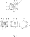
- Fig. 1 an embodiment of the method according to the invention is shown.
- a complete construction of several optoelectronic sensors is to be ensured.
- a PCB benefit 1 which in Fig. 1a is shown.
- the PCB benefit 1 represents a composite of several printed circuit boards 2, which are not isolated yet. In this case, two parallel rows of printed circuit boards 3, 4 are arranged in the circuit board 1 benefits.
- a subsequent step ( Fig. 1b ) the sensor electronics 5 is fitted on each circuit board 2 of the PCB benefit 1 on an SMD line. In this case, the sensor electronics 5 is applied to each individual printed circuit board 2.
- a subsequent step ( Fig. 1c ) terminal and Elektronikternieriata 6 and 7, such as SMD-mountable plugs or line contacting interfaces, such as attachable claws and the like applied.
- the optical components 9 and the mechanical components 8 on the printed circuit boards 2 are populated during a passage through a pick - and - place system or alternatively again by SMD technology.
- the attachment of the individual optical components 9 and the mechanical components 8 can be done for example by mechanical snap elements, displacement ribs or thermosetting adhesive.
- the plate-shaped carrier 10 is formed as a stamped metal sheet, wherein the circuit board 1 is applied to the metal sheet so that the individual circuit boards 2 are placed accurately on prefabricated segments 11 of the metal sheet.
- the board plate 1 reinforced by the metal plate material is inserted into an injection molding tool ( Fig. 1f ).
- an injection molding tool Fig. 1f
- the thin connecting webs of the individual printed circuit boards 2 are punched, so that individual sensor modules 12 are formed, since the individual printed circuit boards 2 are separated from the printed circuit board 1.
- the thus separated sensor modules 12 are fixed in individual cavities of the injection molding tool and molded with a desired housing or material.
- Fig. 1g shows that the electronic and optical components 5, 9 bearing surface of the circuit board 2 with a transparent material encapsulated. But there is also the possibility that only the optical device 9 is provided with a transparent coating, while all other components are covered with an untransparent cover 15.
- the outer wall of the sensor module 12 is completely covered with the encapsulation 16.
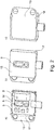
- a further method step is inserted before encapsulation, in which the segments 11 of the metal plate 10 are punched and bent, so that side walls 17 are formed to increase the rigidity of the sensor module 12.
- the segment-shaped metal plate 11 remains free of the encapsulation.
- the cable must be contacted before the encapsulation. Due to the arrangement of two rows of printed circuit boards 3, 4, which face each other on the PCB benefit 1, a formation of the lines of the PCB benefit 1 is chosen away. These attached to the circuit board 2 lines are encapsulated in the encapsulation.
- the present solution allows for easy automation in the manufacture of miniature sensors using the popular SMD or Pickand Place technologies without the use of highly complex devices.
Landscapes
- Engineering & Computer Science (AREA)
- Manufacturing & Machinery (AREA)
- Microelectronics & Electronic Packaging (AREA)
- Non-Metallic Protective Coatings For Printed Circuits (AREA)
- Light Receiving Elements (AREA)
- Injection Moulding Of Plastics Or The Like (AREA)
Abstract
Description
- Die Erfindung betrifft ein Verfahren zur Herstellung von optoelektronischen Sensoren, vorzugsweise Miniatursensoren, bei welchem mehrere in einem Leiterplattennutzen verbundene Leiterplatten automatisch mit elektronischen Bauelementen bestückt werden, welche umspritzt und vereinzelt werden.
- Aus der
DE 10 2008 010 512 A1 ist ein Verfahren zur Herstellung eines optoelektronischen Bauteiles bekannt, wobei jedes optoelektronische Bauteil mindestens einen Halbleiterchip mit einer Chipunterseite sowie mit mindestens zwei elektrischen Kontaktierungen mit Kontaktunterseiten aufweist, wobei sich die Kontaktierungen an der Chipunterseite befinden. Der Halbleiterchip ist mit Ausnahme der Chipunterseite allseitig von einem Vergusskörper umgeben. Die Mehrzahl der Halbleiterchips wird auf einem Träger aufgebracht, der als eine streckbare Sägefolie ausgebildet ist. Durch das Strecken der Folie werden die Halbleiterchips voneinander separiert, so dass gleichmäßige laterale Abstände zwischen den Halbleiterchips auf der Folie entstehen. Danach werden die Halbleiterchips über ein Kompressionsmoldingverfahren umspritzt und anschließend vereinzelt. Die fertigen optoelektronischen Bauteile werden von der Folie nach der Vereinzelung entfernt. - Es wird immer schwieriger, optoelektronische Miniatursensoren auf konventionelle Art und Weise herzustellen. Da ein manuelles Handling der Sub-Miniaturbauteile kaum möglich ist, erfordert eine Einzelsensorfertigung komplexe und filigrane Hilfs- und Automatisierungsvorrichtungen. Dies hat die Folge, dass bei kleiner werdenden Dimensionen nicht eine erwartete Kostensenkung, sondern eine Steigerung der Herstellungskosten mit sich geht.
- Der Erfindung liegt die Aufgabe zugrunde, ein Verfahren zur Herstellung von optoelektronischen Sensoren anzugeben, welches zur Fertigung von Miniatursensoren vollständig automatisch abläuft und auf komplexe Automatisierungsvorrichtungen verzichtet.
- Erfindungsgemäß ist die Aufgabe dadurch gelöst, dass nach der Bestückung der einzelnen Leiterplatten des Leiterplattennutzens mit elektronischen Bauelementen optische und mechanische Bauelemente zum vollständigen Aufbau eines optoelektronischen Sensors auf jeder Leiterplatte des Leiterplattennutzens aufgebracht werden. Dies hat den Vorteil, dass es sich um ein sehr kostengünstiges Automationsverfahren handelt, da bei jedem Arbeitsschritt gleichzeitig eine Vielzahl von optoelektronischen Sensoren mit konventionellen Vorrichtungen bearbeitet wird. Die Miniaturisierung und das Handling der einzelnen optoelektronischen Sensoren werden dabei vereinfacht, da bis zum Abschluss des Herstellungsverfahrens der gesamte Leiterplattennutzen und nicht einzelne Miniaturbauteile behandelt werden.
- Vorteilhafterweise wird nach der Bestückung aller Leiterplatten des Leiterplattennutzens mit allen für den vollständigen Aufbau der Sensoren notwendigen Bauelementen der Leiterplattennutzen auf einem plattenförmigen Trägerelement befestigt. Das Trägerelement bildet dabei gleichzeitig eine Außenwandung des optoelektronischen Sensors.
- In einer Ausgestaltung wird als plattenförmiges Trägerelement eine in Segmente unterteilte hochtemperaturbeständige Platte verwendet, auf welcher der bestückte Leiterplattennutzen so aufgesetzt wird, dass jede einen optoelektronischen Sensor tragende Leiterplatte ein vorgegebenes Segment der hochtemperaturbeständigen Platte ausfüllt. Die hochtemperaturbeständige Platte ist aus einem hochtemperaturbeständigen Werkstoff, beispielsweise einem Polymer oder einem Duroplast. Diese Werkstoffe können den Temperaturen in einem Lötofen, also einem SMD-Ofen während des SMD-Lötprozesses standhalten. Wenn das plattenförmige Trägerelement aus einem solchen spritzgussfähigen Werkstoff besteht wird, vorzugsweise der gleiche Kunststoff auch für die Umspritzung bzw. das Gehäuse verwendet, wodurch eine optimale Verbindung zwischen beiden gebildet wird.
- In einer Ausgestaltung wird als plattenförmiges Trägerelement eine in Segmente unterteilte Metallplatte verwendet, auf welcher der bestückte Leiterplattennutzen so aufgesetzt wird, dass je eine einen optoelektronischen Sensor tragende Leiterplatte ein vorgegebenes Segment der Metallplatte ausfüllt. Die Segmente lassen sich einfach durch einen Stanzvorgang in der Metallplatte ausbilden. Dadurch wird die Herstellung von Miniatursensoren weiter vereinfacht.
- In einer Variante wird der Leiterplattennutzen in ein zwei Formhälften aufweisendes Spritzgusswerkzeug eingelegt, wobei beim Schließen der Formhälften des Spritzgusswerkzeuges die die optoelektronischen Sensoren tragenden Leiterplatten als Sensormodule vereinzelt werden. Dabei wird zum Vereinzeln der Leiterplatten kein eigenständiges Werkzeug benötigt, sondern ein an sich vorhandenes Spritzgusswerkzeug wird genutzt, wodurch die Herstellungskosten weiter reduziert werden.
- In einer Ausführungsform werden die vereinzelten Sensormodule in dem Spritzgusswerkzeug umspritzt. Dadurch entstehen die umspritzten Sensormodule, ohne dass sie vorher einzeln in das Spritzgusswerkzeug eingelegt werden müssen. Dies trägt zur weiteren Senkung der Herstellungskosten bei.
- Vorteilhafterweise bleibt die Metallplatte bzw. die hochtemperaturbeständige Platte des Sensormoduls unumspritzt. Damit kann die Metallplatte bzw. die hochtemperaturbeständige Platte einfach am Anwendungsort des Sensors mit anderen Bauteilen verbunden werden.
- In einer Alternative wird die Metallplatte bzw. die hochtemperaturbeständige Platte vor der Umspritzung zur Bildung wenigstens einer Seitenwandung des Sensormoduls gestanzt oder gebogen. Durch eine solche Seitenwandung wird die Steifigkeit des Sensormoduls verbessert.
- In einer Ausführungsform wird vor der Umspritzung an jedem Sensormodul eine Leitung kontaktiert, wobei die Leitungen jeweils von dem Leiterplattennutzen ? weg gerichtet sind. Durch diese Ausrichtung der Leitungen wird die weitere Bearbeitung der Sensormodule im Spritzgusswerkzeug nicht behindert.
- Vorteilhafterweise werden Anschluss- und Elektrokontaktierelemente mittels SMD-Technologie auf den Leiterplatten des Leiterplattennutzens aufgebracht. Mittels dieser SMD-Technik wird eine geläufige und kostengünstige Technik zur Montage der elektronischen Bauelemente bzw. der Anschluss- und Elektrokontaktierelemente verwendet.
- Die Erfindung lässt zahlreiche Ausführungsformen zu. Eine davon soll anhand der in der Zeichnung dargestellten Figuren näher erläutert werden.
- Es zeigen:
- Fig. 1
- ein erstes Ausführungsbeispiel des erfindungsgemäßen Verfahrens,
- Fig. 2
- ein zweites Ausführungsbeispiel des erfindungsgemäßen Verfahrens.
- In
Fig. 1 ist ein Ausführungsbeispiel des erfindungsgemäßen Verfahrens dargestellt. Mittels dieses Verfahrens soll gleichzeitig ein kompletter Aufbau von mehreren optoelektronischen Sensoren gewährleistet werden. Als Basis für die komplette Sensorfertigung dient dabei ein Leiterplattennutzen 1, welcher inFig. 1a gezeigt ist. Der Leiterplattennutzen 1 stellt einen Verbund von mehreren Leiterplatten 2 dar, die noch nicht vereinzelt sind. In diesem Fall sind zwei parallel zueinander verlaufende Leiterplattenreihen 3, 4 in dem Leiterplattennutzen 1 angeordnet. - In einem sich anschließenden Schritt (
Fig. 1b ) wird die Sensorelektronik 5 auf jeder Leiterplatte 2 des Leiterplattennutzens 1 auf einer SMD-Linie bestückt. Dabei wird die Sensorelektronik 5 auf jeder einzelnen Leiterplatte 2 aufgebracht. In einem anschließenden Schritt (Fig. 1c ) werden Anschluss- und Elektronikkontaktierelemente 6 bzw. 7, wie beispielsweise SMD-bestückbare Stecker oder Leitungskontaktierungsschnittstellen, wie bestückbare Krallen und ähnliches aufgebracht. - Wie aus
Fig. 1d hervorgeht, werden bei einem Durchlauf durch eine Pick - and Place-Anlage oder alternativ wieder durch SMD-Technologie die optischen Bauelemente 9 und die mechanischen Bauteile 8 auf den Leiterplatten 2 bestückt. Die Befestigung der einzelnen optischen Bauelemente 9 und der mechanischen Bauteile 8 kann dabei beispielsweise durch mechanische Schnappelemente, Verdrängungsrippen oder thermisch aushärtendem Klebstoff erfolgen. - Im darauffolgenden Schritt erfolgt eine flächige Verbindung des gesamten vorbestückten Leiterplattennutzens 1 mit einem plattenförmigen Träger 10, wie es in
Fig. 1e gezeigt ist. Der plattenförmige Träger 10 ist als gestanztes Metallblech ausgebildet, wobei der Leiterplattennutzen 1 so auf dem Metallblech aufgebracht wird, dass die einzelnen Leiterplatten 2 auf vorgefertigten Segmenten 11 des Metallblechs genau platziert werden. - Der durch das Metallplattenmaterial verstärkte Leiterplattennutzen 1 wird in ein Spritzgusswerkzeug eingelegt (
Fig. 1f ). Beim Schließen des aus zwei Formhälften bestehenden Spritzgusswerkzeuges werden die dünnen Verbindungsstege der einzelnen Leiterplatten 2 abgestanzt, so dass einzelne Sensormodule 12 entstehen, da die einzelnen Leiterplatten 2 vom Leiterplattennutzen 1 getrennt werden. Die so getrennten Sensormodule 12 werden in einzelnen Hohlräumen des Spritzguss-werkzeuges fixiert und mit einem gewünschten Gehäuse oder Werkstoff umspritzt. Dabei wird, wie ausFig. 1g hervorgeht, die die elektronischen und optischen Bauelemente 5, 9 tragende Oberfläche der Leiterplatte 2 mit einem transparenten Werkstoff umspritzt. Es besteht aber auch die Möglichkeit, dass nur das optische Bauelement 9 mit einer transparenten Beschichtung versehen wird, während alle anderen Bauelemente mit einer untransparenten Abdeckung 15 bedeckt werden. In einer weiteren Alternative ist die Außenwandung des Sensormoduls 12 vollständig mit der Umspritzung 16 bedeckt. - Wie in
Fig. 2 gezeigt, wird vor dem Umspritzen noch ein weiterer Verfahrensschritt eingelegt, bei welchem die Segmente 11 der Metallplatte 10 gestanzt und gebogen werden, so dass Seitenwandungen 17 zur Erhöhung der Steifigkeit des Sensormoduls 12 ausgebildet werden. In diesem Fall bleibt die segmentförmige Metallplatte 11 frei von der Umspritzung. Für etwaige Leitungsvarianten muss vor der Umspritzung die Leitung kontaktiert werden. Aufgrund der Anordnung von zwei Leiterplattenreihen 3, 4, die sich auf dem Leiterplattennutzen 1 gegenüberstehen, wird eine Ausbildung der Leitungen von dem Leiterplattennutzen 1 weg gewählt. Diese an der Leiterplatte 2 befestigten Leitungen werden bei der Umspritzung mit umspritzt. - Die vorliegende Lösung ermöglicht eine einfache Automatisierbarkeit bei der Herstellung von Miniatursensoren unter Nutzung der verbreiteten SMD- bzw. Pickand Place-Technologien ohne die Verwendung von hochkomplexen Vorrichtungen.
Claims (11)
- Verfahren zur Herstellung von optoelektronischen Sensoren, vorzugsweise Miniatursensoren, bei welchem mehrere in einem Leiterplattennutzen (1) verbundene Leiterplatten (2) automatisch mit elektronischen Bauelementen (5) bestückt werden, welche umspritzt und vereinzelt werden, dadurch gekennzeichnet, dass nach der Bestückung der einzelnen Leiterplatten (2) des Leiterplattennutzens (1) mit elektronischen Bauelementen (5) optische und mechanische Bauelemente (9, 8) zum vollständigen Aufbau eines optoelektronischen Sensors auf jeder Leiterplatte (2) des Leiterplattennutzens (1) aufgebracht werden.
- Verfahren nach Anspruch 1, dadurch gekennzeichnet, dass nach der Bestückung aller Leiterplatten (2) des Leiterplattennutzens (1) mit allen für den vollständigen Aufbau der Sensoren notwendigen Bauelementen (5, 6, 7, 8, 9) der Leiterplattennutzen (1) auf einem plattenförmigen Trägerelement (10) befestigt wird.
- Verfahren nach Anspruch 2, dadurch gekennzeichnet, dass als plattenförmiges Trägerelement (10) eine in Segmente (11) unterteilte hochtemperaturbeständige Platte verwendet wird, auf welcher der bestückte Leiterplattennutzen (1) so aufgesetzt wird, dass jede einen optoelektronischen Sensor tragende Leiterplatte (2) ein vorgegebenes Segment (11) der hochtemperaturbeständigen Platte ausfüllt.
- Verfahren nach Anspruch 2, dadurch gekennzeichnet, dass als plattenförmiges Trägerelement (10) eine in Segmente (11) unterteilte Metallplatte verwendet wird, auf welcher der bestückte Leiterplattennutzen (1) so aufgesetzt wird, dass jede einen optoelektronischen Sensor tragende Leiterplatte (2) ein vorgegebenes Segment (11) der Metallplatte ausfüllt.
- Verfahren nach mindestens einem der vorhergehenden Ansprüche, dadurch gekennzeichnet, dass der Leiterplattennutzen (1) in ein zwei Formhälften aufweisendes Spritzgusswerkzeug eingelegt wird, wobei beim Schließen der Formhälften des Spritzgusswerkzeuges die die optoelektronischen Sensoren tragenden Leiterplatten (2) als Sensormodule (12) vereinzelt werden.
- Verfahren nach Anspruch 5, dadurch gekennzeichnet, dass die vereinzelten Sensormodule (12) in dem Spritzgusswerkzeug umspritzt werden.
- Verfahren nach Anspruch 3 oder 4, dadurch gekennzeichnet, dass die Metallplatte (10) oder die hochtemperaturbeständige Platte des Sensormoduls (12) unumspritzt bleibt.
- Verfahren nach Anspruch 3, 4 oder 5, dadurch gekennzeichnet, dass die Metallplatte (10) oder die hochtemperaturbeständige Platte vor der Umspritzung zur Bildung wenigstens einer Seitenwandung (17) des Sensormoduls (12) gestanzt oder gebogen wird.
- Verfahren nach mindestens einem der vorhergehenden Ansprüche, dadurch gekennzeichnet, dass vor der Umspritzung an jedem Sensormodul (12) eine Leitung kontaktiert wird, wobei die Leitungen der Sensormodule (12) jeweils von dem Leiterplattennutzen (1) weg gerichtet sind.
- Verfahren nach mindestens einem der vorhergehenden Ansprüche, dadurch gekennzeichnet, dass Anschluss- und Elektrokontaktierelemente (6, 7) mittels SMD-Technologie auf dem Leiterplattennutzen (1) vor dessen Vereinzelung aufgebracht werden.
- Verfahren nach mindestens einem der vorhergehenden Ansprüche, dadurch gekennzeichnet, dass die elektronischen Bauelemente (5) mittels einer SMD-Technologie auf die Leiterplatten (2) des Leiterplattennutzens (1) aufgebracht werden.
Applications Claiming Priority (1)
| Application Number | Priority Date | Filing Date | Title |
|---|---|---|---|
| DE102017123552.3A DE102017123552B3 (de) | 2017-10-10 | 2017-10-10 | Verfahren zur Herstellung von optoelektronischen Sensoren, insbesondere von Miniatursensoren |
Publications (2)
| Publication Number | Publication Date |
|---|---|
| EP3471518A1 true EP3471518A1 (de) | 2019-04-17 |
| EP3471518B1 EP3471518B1 (de) | 2020-02-26 |
Family
ID=63678389
Family Applications (1)
| Application Number | Title | Priority Date | Filing Date |
|---|---|---|---|
| EP18194292.1A Active EP3471518B1 (de) | 2017-10-10 | 2018-09-13 | Verfahren zur herstellung von optoelektronischen sensoren, insbesondere von miniatursensoren |
Country Status (2)
| Country | Link |
|---|---|
| EP (1) | EP3471518B1 (de) |
| DE (1) | DE102017123552B3 (de) |
Families Citing this family (2)
| Publication number | Priority date | Publication date | Assignee | Title |
|---|---|---|---|---|
| DE102020214020A1 (de) | 2020-11-09 | 2022-05-12 | Robert Bosch Gesellschaft mit beschränkter Haftung | Positionssensor und Führungswagen mit einem Positionssensor und Verfahren zur Herstellung eines Positionssensors |
| DE102024203630B3 (de) * | 2024-04-18 | 2025-08-21 | Aumovio Autonomous Mobility Germany Gmbh | Verfahren zur Herstellung einer Sensorbaugruppe |
Citations (6)
| Publication number | Priority date | Publication date | Assignee | Title |
|---|---|---|---|---|
| WO2006101274A1 (en) * | 2005-03-25 | 2006-09-28 | Fujifilm Corporation | Method of manufacturing solid state imaging device |
| US20070004095A1 (en) * | 2005-06-30 | 2007-01-04 | Foehringer Richard B | Packaging method and apparatus |
| DE102009059236A1 (de) * | 2008-12-23 | 2010-07-01 | Infineon Technologies Ag | Verfahren zum Herstellen eines Halbleiterbauelements und Halbleiterbauelement |
| US20150043228A1 (en) * | 2013-08-08 | 2015-02-12 | Kabushiki Kaisha Toshiba | Semiconductor device, and method of manufacturing semiconductor device |
| US9105613B1 (en) * | 2014-07-30 | 2015-08-11 | Advanced Semiconductor Engineering Inc. | Method of manufacturing electronic package module and electronic package module manufactured by the same |
| US20150262984A1 (en) * | 2014-03-14 | 2015-09-17 | Avago Technologies General Ip (Singapore) Pte. Ltd. | METHODS FOR PERFORMING EMBEDDED WAFER-LEVEL PACKAGING (eWLP) AND eWLP DEVICES, PACKAGES AND ASSEMBLIES MADE BY THE METHODS |
Family Cites Families (2)
| Publication number | Priority date | Publication date | Assignee | Title |
|---|---|---|---|---|
| DE102005054177B4 (de) | 2005-11-14 | 2011-12-22 | Infineon Technologies Ag | Verfahren zum Herstellen einer Vielzahl von gehäusten Sensormodulen |
| DE102008010512A1 (de) | 2008-02-22 | 2009-08-27 | Osram Opto Semiconductors Gmbh | Optoelektronisches Bauteil und Verfahren zur Herstellung eines optoelektronischen Bauteils |
-
2017
- 2017-10-10 DE DE102017123552.3A patent/DE102017123552B3/de active Active
-
2018
- 2018-09-13 EP EP18194292.1A patent/EP3471518B1/de active Active
Patent Citations (6)
| Publication number | Priority date | Publication date | Assignee | Title |
|---|---|---|---|---|
| WO2006101274A1 (en) * | 2005-03-25 | 2006-09-28 | Fujifilm Corporation | Method of manufacturing solid state imaging device |
| US20070004095A1 (en) * | 2005-06-30 | 2007-01-04 | Foehringer Richard B | Packaging method and apparatus |
| DE102009059236A1 (de) * | 2008-12-23 | 2010-07-01 | Infineon Technologies Ag | Verfahren zum Herstellen eines Halbleiterbauelements und Halbleiterbauelement |
| US20150043228A1 (en) * | 2013-08-08 | 2015-02-12 | Kabushiki Kaisha Toshiba | Semiconductor device, and method of manufacturing semiconductor device |
| US20150262984A1 (en) * | 2014-03-14 | 2015-09-17 | Avago Technologies General Ip (Singapore) Pte. Ltd. | METHODS FOR PERFORMING EMBEDDED WAFER-LEVEL PACKAGING (eWLP) AND eWLP DEVICES, PACKAGES AND ASSEMBLIES MADE BY THE METHODS |
| US9105613B1 (en) * | 2014-07-30 | 2015-08-11 | Advanced Semiconductor Engineering Inc. | Method of manufacturing electronic package module and electronic package module manufactured by the same |
Also Published As
| Publication number | Publication date |
|---|---|
| DE102017123552B3 (de) | 2018-11-22 |
| EP3471518B1 (de) | 2020-02-26 |
Similar Documents
| Publication | Publication Date | Title |
|---|---|---|
| EP2163145B1 (de) | Elektronikmodul und verfahren zur herstellung eines elektronikmoduls | |
| EP3329751B1 (de) | Elektronikmodul mit über sockelelement flexibel platzierbarem bauelement und verfahren zum fertigen desselben | |
| EP0706214A2 (de) | Elektronikmodul und Chipkarte | |
| EP1199913A2 (de) | Verfahren zur Herstellung von Leiterfolie-Trägergehäuse-Einheiten | |
| EP2819492B1 (de) | MID-Bauteil, Verfahren zur Herstellung | |
| DE112016002445T5 (de) | Sensorvorrichtung | |
| EP3695692A1 (de) | Verfahren zur mechanischen kontaktierung eines vergussrahmens auf einer leiterplatte | |
| EP2265102A1 (de) | Sensoraufbau ohne Gehäuse | |
| DE102017123552B3 (de) | Verfahren zur Herstellung von optoelektronischen Sensoren, insbesondere von Miniatursensoren | |
| EP0649719B1 (de) | Verfahren zur Herstellung von Chipkarten mittels Spritzgiessen | |
| DE102009046870A1 (de) | Elektronisches Schaltgerät mit Anschlusskabel | |
| WO2014049059A2 (de) | Bauteilanordnung und verfahren zum herstellen von elektrischen bauteilen | |
| DE102016224949B4 (de) | Verfahren zur Herstellung von mechatronischen Baugruppen | |
| DE102007035794A1 (de) | Leiterplattenverbund sowie Verfahren zum Herstellen eines Leiterplattenverbundes | |
| EP2215008B1 (de) | Modulgehäuse und verfahren zur herstellung eines modulgehäuses | |
| DE102015207873A1 (de) | Elektronikmodul für ein Getriebesteuergerät | |
| EP2243342B1 (de) | Elektronisches bauteil und verfahren zur herstellung des elektronischen bauteiles | |
| DE102007025890B4 (de) | Steuergerät für ein Kraftfahrzeug und Anordnung des Steuergeräts an einer Systemschnittstelle | |
| EP3284327B1 (de) | Elektronikmodul für ein getriebesteuergerät | |
| EP3411903B1 (de) | Moldmodul, verfahren zur herstellung eines moldmoduls und moldwerkzeug für die moldumspritzung eines moldmoduls | |
| WO2007054557A1 (de) | Sensorbaugruppe | |
| WO2016075114A1 (de) | Verfahren zum herstellen eines trägers und verfahren zum herstellen eines optoelektronischen bauelements | |
| DE19742470A1 (de) | Verfahren zum Herstellen eines elektrischen Gerätes mit Gehäuse | |
| CH686462A5 (de) | Elektronikmodul und Chip-Karte. | |
| WO2017001113A1 (de) | Schaltungsträger für eine elektronische schaltung und verfahren zum herstellen eines derartigen schaltungsträgers |
Legal Events
| Date | Code | Title | Description |
|---|---|---|---|
| PUAI | Public reference made under article 153(3) epc to a published international application that has entered the european phase |
Free format text: ORIGINAL CODE: 0009012 |
|
| STAA | Information on the status of an ep patent application or granted ep patent |
Free format text: STATUS: THE APPLICATION HAS BEEN PUBLISHED |
|
| AK | Designated contracting states |
Kind code of ref document: A1 Designated state(s): AL AT BE BG CH CY CZ DE DK EE ES FI FR GB GR HR HU IE IS IT LI LT LU LV MC MK MT NL NO PL PT RO RS SE SI SK SM TR |
|
| AX | Request for extension of the european patent |
Extension state: BA ME |
|
| STAA | Information on the status of an ep patent application or granted ep patent |
Free format text: STATUS: REQUEST FOR EXAMINATION WAS MADE |
|
| 17P | Request for examination filed |
Effective date: 20190625 |
|
| RBV | Designated contracting states (corrected) |
Designated state(s): AL AT BE BG CH CY CZ DE DK EE ES FI FR GB GR HR HU IE IS IT LI LT LU LV MC MK MT NL NO PL PT RO RS SE SI SK SM TR |
|
| RIC1 | Information provided on ipc code assigned before grant |
Ipc: H05K 3/34 20060101ALN20190912BHEP Ipc: H01L 21/56 20060101ALI20190912BHEP Ipc: H01L 23/31 20060101ALI20190912BHEP Ipc: H01L 23/00 20060101ALI20190912BHEP Ipc: H05K 3/00 20060101AFI20190912BHEP Ipc: H05K 1/18 20060101ALN20190912BHEP Ipc: H05K 3/28 20060101ALI20190912BHEP Ipc: H01L 31/167 20060101ALI20190912BHEP Ipc: H01L 31/0203 20140101ALI20190912BHEP |
|
| GRAP | Despatch of communication of intention to grant a patent |
Free format text: ORIGINAL CODE: EPIDOSNIGR1 |
|
| STAA | Information on the status of an ep patent application or granted ep patent |
Free format text: STATUS: GRANT OF PATENT IS INTENDED |
|
| RIC1 | Information provided on ipc code assigned before grant |
Ipc: H05K 3/00 20060101AFI20190917BHEP Ipc: H01L 23/00 20060101ALI20190917BHEP Ipc: H01L 31/167 20060101ALI20190917BHEP Ipc: H05K 1/18 20060101ALN20190917BHEP Ipc: H01L 21/56 20060101ALI20190917BHEP Ipc: H01L 23/31 20060101ALI20190917BHEP Ipc: B29C 45/14 20060101ALN20190917BHEP Ipc: H05K 3/34 20060101ALN20190917BHEP Ipc: H01L 31/0203 20140101ALI20190917BHEP Ipc: H05K 3/28 20060101ALI20190917BHEP |
|
| RIC1 | Information provided on ipc code assigned before grant |
Ipc: H01L 31/167 20060101ALI20190923BHEP Ipc: H01L 31/0203 20140101ALI20190923BHEP Ipc: H05K 3/00 20060101AFI20190923BHEP Ipc: H05K 1/18 20060101ALN20190923BHEP Ipc: H05K 3/28 20060101ALI20190923BHEP Ipc: H05K 3/34 20060101ALN20190923BHEP Ipc: B29C 45/14 20060101ALN20190923BHEP Ipc: H01L 21/56 20060101ALI20190923BHEP Ipc: H01L 23/31 20060101ALI20190923BHEP Ipc: H01L 23/00 20060101ALI20190923BHEP |
|
| RIC1 | Information provided on ipc code assigned before grant |
Ipc: H05K 1/18 20060101ALN20190930BHEP Ipc: B29C 45/14 20060101ALN20190930BHEP Ipc: H01L 31/167 20060101ALI20190930BHEP Ipc: H05K 3/00 20060101AFI20190930BHEP Ipc: H01L 31/0203 20140101ALI20190930BHEP Ipc: H05K 3/34 20060101ALN20190930BHEP Ipc: H01L 21/56 20060101ALI20190930BHEP Ipc: H05K 3/28 20060101ALI20190930BHEP Ipc: H01L 23/00 20060101ALI20190930BHEP Ipc: H01L 23/31 20060101ALI20190930BHEP |
|
| INTG | Intention to grant announced |
Effective date: 20191021 |
|
| GRAS | Grant fee paid |
Free format text: ORIGINAL CODE: EPIDOSNIGR3 |
|
| GRAA | (expected) grant |
Free format text: ORIGINAL CODE: 0009210 |
|
| STAA | Information on the status of an ep patent application or granted ep patent |
Free format text: STATUS: THE PATENT HAS BEEN GRANTED |
|
| RAP1 | Party data changed (applicant data changed or rights of an application transferred) |
Owner name: SICK AG |
|
| AK | Designated contracting states |
Kind code of ref document: B1 Designated state(s): AL AT BE BG CH CY CZ DE DK EE ES FI FR GB GR HR HU IE IS IT LI LT LU LV MC MK MT NL NO PL PT RO RS SE SI SK SM TR |
|
| REG | Reference to a national code |
Ref country code: GB Ref legal event code: FG4D Free format text: NOT ENGLISH |
|
| REG | Reference to a national code |
Ref country code: CH Ref legal event code: EP |
|
| REG | Reference to a national code |
Ref country code: AT Ref legal event code: REF Ref document number: 1239314 Country of ref document: AT Kind code of ref document: T Effective date: 20200315 |
|
| REG | Reference to a national code |
Ref country code: IE Ref legal event code: FG4D Free format text: LANGUAGE OF EP DOCUMENT: GERMAN |
|
| REG | Reference to a national code |
Ref country code: DE Ref legal event code: R096 Ref document number: 502018000835 Country of ref document: DE |
|
| PG25 | Lapsed in a contracting state [announced via postgrant information from national office to epo] |
Ref country code: RS Free format text: LAPSE BECAUSE OF FAILURE TO SUBMIT A TRANSLATION OF THE DESCRIPTION OR TO PAY THE FEE WITHIN THE PRESCRIBED TIME-LIMIT Effective date: 20200226 Ref country code: FI Free format text: LAPSE BECAUSE OF FAILURE TO SUBMIT A TRANSLATION OF THE DESCRIPTION OR TO PAY THE FEE WITHIN THE PRESCRIBED TIME-LIMIT Effective date: 20200226 Ref country code: NO Free format text: LAPSE BECAUSE OF FAILURE TO SUBMIT A TRANSLATION OF THE DESCRIPTION OR TO PAY THE FEE WITHIN THE PRESCRIBED TIME-LIMIT Effective date: 20200526 |
|
| REG | Reference to a national code |
Ref country code: NL Ref legal event code: MP Effective date: 20200226 |
|
| REG | Reference to a national code |
Ref country code: LT Ref legal event code: MG4D |
|
| PG25 | Lapsed in a contracting state [announced via postgrant information from national office to epo] |
Ref country code: BG Free format text: LAPSE BECAUSE OF FAILURE TO SUBMIT A TRANSLATION OF THE DESCRIPTION OR TO PAY THE FEE WITHIN THE PRESCRIBED TIME-LIMIT Effective date: 20200526 Ref country code: HR Free format text: LAPSE BECAUSE OF FAILURE TO SUBMIT A TRANSLATION OF THE DESCRIPTION OR TO PAY THE FEE WITHIN THE PRESCRIBED TIME-LIMIT Effective date: 20200226 Ref country code: LV Free format text: LAPSE BECAUSE OF FAILURE TO SUBMIT A TRANSLATION OF THE DESCRIPTION OR TO PAY THE FEE WITHIN THE PRESCRIBED TIME-LIMIT Effective date: 20200226 Ref country code: IS Free format text: LAPSE BECAUSE OF FAILURE TO SUBMIT A TRANSLATION OF THE DESCRIPTION OR TO PAY THE FEE WITHIN THE PRESCRIBED TIME-LIMIT Effective date: 20200626 Ref country code: SE Free format text: LAPSE BECAUSE OF FAILURE TO SUBMIT A TRANSLATION OF THE DESCRIPTION OR TO PAY THE FEE WITHIN THE PRESCRIBED TIME-LIMIT Effective date: 20200226 Ref country code: GR Free format text: LAPSE BECAUSE OF FAILURE TO SUBMIT A TRANSLATION OF THE DESCRIPTION OR TO PAY THE FEE WITHIN THE PRESCRIBED TIME-LIMIT Effective date: 20200527 |
|
| PG25 | Lapsed in a contracting state [announced via postgrant information from national office to epo] |
Ref country code: NL Free format text: LAPSE BECAUSE OF FAILURE TO SUBMIT A TRANSLATION OF THE DESCRIPTION OR TO PAY THE FEE WITHIN THE PRESCRIBED TIME-LIMIT Effective date: 20200226 |
|
| PG25 | Lapsed in a contracting state [announced via postgrant information from national office to epo] |
Ref country code: SM Free format text: LAPSE BECAUSE OF FAILURE TO SUBMIT A TRANSLATION OF THE DESCRIPTION OR TO PAY THE FEE WITHIN THE PRESCRIBED TIME-LIMIT Effective date: 20200226 Ref country code: SK Free format text: LAPSE BECAUSE OF FAILURE TO SUBMIT A TRANSLATION OF THE DESCRIPTION OR TO PAY THE FEE WITHIN THE PRESCRIBED TIME-LIMIT Effective date: 20200226 Ref country code: RO Free format text: LAPSE BECAUSE OF FAILURE TO SUBMIT A TRANSLATION OF THE DESCRIPTION OR TO PAY THE FEE WITHIN THE PRESCRIBED TIME-LIMIT Effective date: 20200226 Ref country code: EE Free format text: LAPSE BECAUSE OF FAILURE TO SUBMIT A TRANSLATION OF THE DESCRIPTION OR TO PAY THE FEE WITHIN THE PRESCRIBED TIME-LIMIT Effective date: 20200226 Ref country code: DK Free format text: LAPSE BECAUSE OF FAILURE TO SUBMIT A TRANSLATION OF THE DESCRIPTION OR TO PAY THE FEE WITHIN THE PRESCRIBED TIME-LIMIT Effective date: 20200226 Ref country code: ES Free format text: LAPSE BECAUSE OF FAILURE TO SUBMIT A TRANSLATION OF THE DESCRIPTION OR TO PAY THE FEE WITHIN THE PRESCRIBED TIME-LIMIT Effective date: 20200226 Ref country code: CZ Free format text: LAPSE BECAUSE OF FAILURE TO SUBMIT A TRANSLATION OF THE DESCRIPTION OR TO PAY THE FEE WITHIN THE PRESCRIBED TIME-LIMIT Effective date: 20200226 Ref country code: LT Free format text: LAPSE BECAUSE OF FAILURE TO SUBMIT A TRANSLATION OF THE DESCRIPTION OR TO PAY THE FEE WITHIN THE PRESCRIBED TIME-LIMIT Effective date: 20200226 Ref country code: PT Free format text: LAPSE BECAUSE OF FAILURE TO SUBMIT A TRANSLATION OF THE DESCRIPTION OR TO PAY THE FEE WITHIN THE PRESCRIBED TIME-LIMIT Effective date: 20200719 |
|
| REG | Reference to a national code |
Ref country code: DE Ref legal event code: R097 Ref document number: 502018000835 Country of ref document: DE |
|
| PLBE | No opposition filed within time limit |
Free format text: ORIGINAL CODE: 0009261 |
|
| STAA | Information on the status of an ep patent application or granted ep patent |
Free format text: STATUS: NO OPPOSITION FILED WITHIN TIME LIMIT |
|
| 26N | No opposition filed |
Effective date: 20201127 |
|
| PG25 | Lapsed in a contracting state [announced via postgrant information from national office to epo] |
Ref country code: SI Free format text: LAPSE BECAUSE OF FAILURE TO SUBMIT A TRANSLATION OF THE DESCRIPTION OR TO PAY THE FEE WITHIN THE PRESCRIBED TIME-LIMIT Effective date: 20200226 Ref country code: PL Free format text: LAPSE BECAUSE OF FAILURE TO SUBMIT A TRANSLATION OF THE DESCRIPTION OR TO PAY THE FEE WITHIN THE PRESCRIBED TIME-LIMIT Effective date: 20200226 |
|
| REG | Reference to a national code |
Ref country code: BE Ref legal event code: MM Effective date: 20200930 |
|
| PG25 | Lapsed in a contracting state [announced via postgrant information from national office to epo] |
Ref country code: LU Free format text: LAPSE BECAUSE OF NON-PAYMENT OF DUE FEES Effective date: 20200913 |
|
| PG25 | Lapsed in a contracting state [announced via postgrant information from national office to epo] |
Ref country code: BE Free format text: LAPSE BECAUSE OF NON-PAYMENT OF DUE FEES Effective date: 20200930 Ref country code: IE Free format text: LAPSE BECAUSE OF NON-PAYMENT OF DUE FEES Effective date: 20200913 |
|
| REG | Reference to a national code |
Ref country code: CH Ref legal event code: PL |
|
| PG25 | Lapsed in a contracting state [announced via postgrant information from national office to epo] |
Ref country code: TR Free format text: LAPSE BECAUSE OF FAILURE TO SUBMIT A TRANSLATION OF THE DESCRIPTION OR TO PAY THE FEE WITHIN THE PRESCRIBED TIME-LIMIT Effective date: 20200226 Ref country code: MT Free format text: LAPSE BECAUSE OF FAILURE TO SUBMIT A TRANSLATION OF THE DESCRIPTION OR TO PAY THE FEE WITHIN THE PRESCRIBED TIME-LIMIT Effective date: 20200226 Ref country code: CY Free format text: LAPSE BECAUSE OF FAILURE TO SUBMIT A TRANSLATION OF THE DESCRIPTION OR TO PAY THE FEE WITHIN THE PRESCRIBED TIME-LIMIT Effective date: 20200226 |
|
| PG25 | Lapsed in a contracting state [announced via postgrant information from national office to epo] |
Ref country code: MK Free format text: LAPSE BECAUSE OF FAILURE TO SUBMIT A TRANSLATION OF THE DESCRIPTION OR TO PAY THE FEE WITHIN THE PRESCRIBED TIME-LIMIT Effective date: 20200226 Ref country code: MC Free format text: LAPSE BECAUSE OF FAILURE TO SUBMIT A TRANSLATION OF THE DESCRIPTION OR TO PAY THE FEE WITHIN THE PRESCRIBED TIME-LIMIT Effective date: 20200226 Ref country code: AL Free format text: LAPSE BECAUSE OF FAILURE TO SUBMIT A TRANSLATION OF THE DESCRIPTION OR TO PAY THE FEE WITHIN THE PRESCRIBED TIME-LIMIT Effective date: 20200226 |
|
| PG25 | Lapsed in a contracting state [announced via postgrant information from national office to epo] |
Ref country code: LI Free format text: LAPSE BECAUSE OF NON-PAYMENT OF DUE FEES Effective date: 20210930 Ref country code: CH Free format text: LAPSE BECAUSE OF NON-PAYMENT OF DUE FEES Effective date: 20210930 |
|
| GBPC | Gb: european patent ceased through non-payment of renewal fee |
Effective date: 20220913 |
|
| PG25 | Lapsed in a contracting state [announced via postgrant information from national office to epo] |
Ref country code: GB Free format text: LAPSE BECAUSE OF NON-PAYMENT OF DUE FEES Effective date: 20220913 |
|
| REG | Reference to a national code |
Ref country code: AT Ref legal event code: MM01 Ref document number: 1239314 Country of ref document: AT Kind code of ref document: T Effective date: 20230913 |
|
| PG25 | Lapsed in a contracting state [announced via postgrant information from national office to epo] |
Ref country code: AT Free format text: LAPSE BECAUSE OF NON-PAYMENT OF DUE FEES Effective date: 20230913 |
|
| PG25 | Lapsed in a contracting state [announced via postgrant information from national office to epo] |
Ref country code: AT Free format text: LAPSE BECAUSE OF NON-PAYMENT OF DUE FEES Effective date: 20230913 |
|
| PGFP | Annual fee paid to national office [announced via postgrant information from national office to epo] |
Ref country code: DE Payment date: 20250919 Year of fee payment: 8 |
|
| PGFP | Annual fee paid to national office [announced via postgrant information from national office to epo] |
Ref country code: FR Payment date: 20250922 Year of fee payment: 8 |
|
| PGFP | Annual fee paid to national office [announced via postgrant information from national office to epo] |
Ref country code: IT Payment date: 20250930 Year of fee payment: 8 |
|
| PGFP | Annual fee paid to national office [announced via postgrant information from national office to epo] |
Ref country code: AT Payment date: 20260410 Year of fee payment: 5 |