EP3471226A1 - Integrally bonded and installed protective enclosure - Google Patents
Integrally bonded and installed protective enclosure Download PDFInfo
- Publication number
- EP3471226A1 EP3471226A1 EP18199690.1A EP18199690A EP3471226A1 EP 3471226 A1 EP3471226 A1 EP 3471226A1 EP 18199690 A EP18199690 A EP 18199690A EP 3471226 A1 EP3471226 A1 EP 3471226A1
- Authority
- EP
- European Patent Office
- Prior art keywords
- enclosure
- base
- conductive element
- potting material
- electrically
- Prior art date
- Legal status (The legal status is an assumption and is not a legal conclusion. Google has not performed a legal analysis and makes no representation as to the accuracy of the status listed.)
- Granted
Links
Images


Classifications
-
- H—ELECTRICITY
- H02—GENERATION; CONVERSION OR DISTRIBUTION OF ELECTRIC POWER
- H02G—INSTALLATION OF ELECTRIC CABLES OR LINES, OR OF COMBINED OPTICAL AND ELECTRIC CABLES OR LINES
- H02G15/00—Cable fittings
- H02G15/007—Devices for relieving mechanical stress
-
- H—ELECTRICITY
- H05—ELECTRIC TECHNIQUES NOT OTHERWISE PROVIDED FOR
- H05K—PRINTED CIRCUITS; CASINGS OR CONSTRUCTIONAL DETAILS OF ELECTRIC APPARATUS; MANUFACTURE OF ASSEMBLAGES OF ELECTRICAL COMPONENTS
- H05K5/00—Casings, cabinets or drawers for electric apparatus
- H05K5/0026—Casings, cabinets or drawers for electric apparatus provided with connectors and printed circuit boards [PCB], e.g. automotive electronic control units
- H05K5/0047—Casings, cabinets or drawers for electric apparatus provided with connectors and printed circuit boards [PCB], e.g. automotive electronic control units having a two-part housing enclosing a PCB
- H05K5/0056—Casings, cabinets or drawers for electric apparatus provided with connectors and printed circuit boards [PCB], e.g. automotive electronic control units having a two-part housing enclosing a PCB characterized by features for protecting electronic components against vibration and moisture, e.g. potting, holders for relatively large capacitors
-
- H—ELECTRICITY
- H01—ELECTRIC ELEMENTS
- H01R—ELECTRICALLY-CONDUCTIVE CONNECTIONS; STRUCTURAL ASSOCIATIONS OF A PLURALITY OF MUTUALLY-INSULATED ELECTRICAL CONNECTING ELEMENTS; COUPLING DEVICES; CURRENT COLLECTORS
- H01R13/00—Details of coupling devices of the kinds covered by groups H01R12/70 or H01R24/00 - H01R33/00
- H01R13/66—Structural association with built-in electrical component
-
- H—ELECTRICITY
- H02—GENERATION; CONVERSION OR DISTRIBUTION OF ELECTRIC POWER
- H02G—INSTALLATION OF ELECTRIC CABLES OR LINES, OR OF COMBINED OPTICAL AND ELECTRIC CABLES OR LINES
- H02G15/00—Cable fittings
- H02G15/013—Sealing means for cable inlets
-
- H—ELECTRICITY
- H05—ELECTRIC TECHNIQUES NOT OTHERWISE PROVIDED FOR
- H05K—PRINTED CIRCUITS; CASINGS OR CONSTRUCTIONAL DETAILS OF ELECTRIC APPARATUS; MANUFACTURE OF ASSEMBLAGES OF ELECTRICAL COMPONENTS
- H05K5/00—Casings, cabinets or drawers for electric apparatus
- H05K5/06—Hermetically-sealed casings
- H05K5/064—Hermetically-sealed casings sealed by potting, e.g. waterproof resin poured in a rigid casing
-
- H—ELECTRICITY
- H05—ELECTRIC TECHNIQUES NOT OTHERWISE PROVIDED FOR
- H05K—PRINTED CIRCUITS; CASINGS OR CONSTRUCTIONAL DETAILS OF ELECTRIC APPARATUS; MANUFACTURE OF ASSEMBLAGES OF ELECTRICAL COMPONENTS
- H05K7/00—Constructional details common to different types of electric apparatus
- H05K7/14—Mounting supporting structure in casing or on frame or rack
Definitions
- Aircraft wiring can be subjected to flexing, displacement, and other stresses, as well as extreme operating conditions, depending on the type of aircraft and aircraft system. Electrical wiring can be protected using strain relief devices, such as clamps, or encapsulation in a potting material. Current potting molds can be cumbersome, and often require removal of the mold and further processing of the cured potting material. These molds may be prone to leaking or pooling of uncured potting material. Potted areas may also be sensitive to poor bonding, which can result in structural or electrical connection failures and/or moisture intrusion.
- a protective enclosure for an electrically-conductive element disposed along a component surface includes a base, a first side with an electrical connector, and a second side with an aperture for receiving a potting material.
- the base, the first side, and the second side at least partially define an internal void, and the internal void communicates with an external environment via the aperture.
- a method of making a protective enclosure for an electrically-conductive element disposed along a component surface includes forming a base, forming a first side with an electrical connector, and forming a second side with an aperture extending therethrough. The method further includes connecting the base, the first side, and the second side such that they at least partially form an internal void.
- the present invention is directed to a potting mold designed to enclose electrical wiring or other electrical components.
- the potting mold can be formed to fit the dimensions of a specific area, using less material and taking up less space than traditional molds. Once filled with the potting material, the mold protects and relieves strain on potted components.
- the mold can include internal features used to help anchor or support enclosed components.
- FIG. 1 is a perspective view of potting enclosure 10 mounted to panel 12 such that surface 14 of panel 12 is in contact with base 16 of enclosure 10.
- Panel 12 can be a heated floor panel, for example, or another planar structure that receives wires or cables.
- Enclosure 10 includes connector side 18 and fill side 20.
- Connector 22 is mounted to connector side 18, and is configured to connect an external portion 26 E of conductive element 24 with internal portion 26 I (shown in FIG. 2 ).
- connector 22 can be an integral part of connector side 22. It can be alternatively be made to accommodate a "flying lead" such that it is formed as an opening within connector side 18 through which conductive element 24 can be passed.
- Fill side 20 includes apertures 28 through which potting material can be introduced into enclosure 10.
- enclosure 10 can include a single aperture 28, or more than two apertures 28 on one or more fill sides 20.
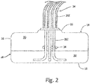
- FIG. 2 is a simplified cross-section of enclosure 10, shown detached from panel 12. As can be seen in FIG. 2 , the various sides of enclosure 10 form internal void 30.
- conductive element 24 is a group of electrical wires with external and internal portions 26 E and 26 I , respectively, meeting at connector 22. The external portion 26 E of conductive element 24 is harnessed, while the wires of conductive element 24 are separated within void 30 to form internal portion 26 I .
- conductive element 24 can include a single wire, or a group of wires that remain bundled within void 30.
- conductive element 24 can generally be an electrical element, such as a coil, a capacitor, a rectifier, or a sensor, to name a few, non-limiting examples.
- Potting material 32 is introduced to void 30 via one or more apertures 28.
- potting material 32 occupies only a portion of void 30, covering part of internal portion 26 I of wires 24. In other embodiments, potting material 32 can occupy less or more of the volume of void 30, depending on factors such as the type of conductive element 24, orientation of enclosure 10, or operating environment. Once cured, potting material 32 helps reduce strain on conductive element 24 from vibration, impact, or other movement. Potting material 32 also protects conductive element 24 from moisture and other contaminants.
- Potting material 32 can be an epoxy-based material, and can include single or multi-component epoxy systems. Potting material 32 can further include foaming and/or expanding epoxies that are lighter in weight than other epoxies. For certain applications, such as for use inside an aircraft fuselage, potting material 32 can be a fire resistant, low smoke/toxicity (FST-type) epoxy. In other embodiments, potting material 32 can be a polymer-based material, such as silicones, urethanes, polyamides, butyls, and polyolefins, to name a few, non-limiting examples.
- FST-type fire resistant, low smoke/toxicity
- Enclosure 10 can include restraint 34 within void 30.
- Restraint 34 is an anchoring mechanism that can be used to properly position and hold conductive element 24 in place before and during the curing period of potting material 32. Restraint 34 can also generally provide additional strain relief for conductive element 24.
- restraint 34 is a clamp-like device, but can also be configured as a hook, loop, bushing, or other suitable restraint.
- enclosure 10 can also include a plurality of restraints 34.
- restraint 34 can include one or more restraints located on the exterior of enclosure 10 allowing for the restraint of a service loop in element 24, or it can serve as an anchor point for supplemental components.
- FIG. 3 is a perspective view of alternative enclosure 110, attached to workpiece 112, which can be, for example, a leading edge of an aircraft component.
- enclosure 110 is attached at its base 116 to an inner surface 114 of workpiece 112.
- base 116 is curved to match the curvature of inner surface 114.
- Enclosure 110 includes connector side 118 and connector 122. Although shown (for simplicity) without a conductive element, connector 122 is configured to interface with the types of the conductive elements 24 referenced above with respect to enclosure 10.
- connector side 118 is generally orthogonal to base 116, but could be formed as parallel to base 116, as is shown in the embodiments of FIGS. 1 and 2 .
- Enclosure 110 also includes fill side 120 having apertures 128. As with enclosure 10, fill side 120 can include only a single aperture, or have more than two apertures arranged on one or more sides of enclosure 110.
- enclosure 110 can be formed from a material that is at least partially transparent. Using such a material allows for viewing of the internal components and the potting process. This can be useful for facilitating proper placement of enclosure 110 over or around electrical components, and for ensuring desired coverage of the components by the potting material. Operators can continue to view the potted area through enclosure 110, which, like enclosure 10, is intended to remain situated over potted components. Although shown in FIG. 1 as an opaque structure, it is also possible for enclosure 10 to be formed from a transparent material.
- Enclosures 10, 110 can be formed using a 3D printing technique. Specifically, enclosures 10, 110 can be formed using a vat photopolymerization technique, such as stereolithography. By using 3D printing, enclosures 10, 110 can be formed to the exact dimensions of a specific area, and can be made to accommodate many types of electrical and other components. Enclosures 10, 110 can be made to have thinner walls/sides than traditional molds. Also unlike traditional molds, enclosures 10, 110 can have localized variations in wall thicknesses. For example, it may be desirable to make one side of enclosure 10, 110 thicker in certain areas, or thicker, altogether, than the remaining sides, depending on the surrounding environment and potential hazards.
- Materials used to form enclosures 10, 110 can include polymers, such as polyamides, acrylonitrile-butadiene-styrene (ABS), and polyurethanes.
- the materials can also include resin only and/or reinforced epoxies or phenolics. Other suitable materials are contemplated herein.
- Bases 16, 116 can be contoured to match the surface to which they are attached. This includes planar surfaces, such as panel 12, or curved surfaces, such as workpiece 112. Other shapes or contours are contemplated herein. As is shown in FIGS. 1 and 3 , bases 16, 116 can also be flanged such that they extend beyond one or more of the generally orthogonal sides of enclosure 10, 110.
- the specific footprint of the flanged bases can be optimized to balance weight and spatial impact against the surface area required to ensure proper bonding under the loading conditions of panel 12 or workpiece 112.
- the use of 3D printing also allows for "enhancements" such as internal or external restraints or fasteners, or transparent build material.
- enclosures 10, 110 are placed over or around the area and components to be protected, and are attached to the corresponding surface using, for example, and adhesive. Other bonding techniques are contemplated herein. In some cases, enclosures 10, 110 can completely surround the conductive element, and need not be attached to another structure. Once attached, the desired amount of potting material can be added and allowed to cure. Unlike traditional molds, enclosures 10, 110 need not be removed after curing is complete, but can be removed if so desired.
- the disclosed potting enclosures have many advantages. First, they can be formed to exact dimensions of the area to be protected, and can be contoured for mounting on planar or non-planar surfaces. Enclosure walls can be made thinner than those of traditional molds. Due to their tailored design, the disclosed enclosures are less prone to leaking. In addition to aerospace applications, the disclosed enclosures can be used in other transportation industries, or any application requiring encapsulation of electrical components.
- a protective enclosure for an electrically-conductive element disposed along a component surface includes a base, a first side with an electrical connector, and a second side with an aperture for receiving a potting material.
- the base, the first side, and the second side at least partially define an internal void, and the internal void communicates with an external environment via the aperture.
- the enclosure of the preceding paragraph can optionally include, additionally and/or alternatively, any one or more of the following features, configurations and/or additional components:
- the base is mountable to the component surface.
- the electrically-conductive element includes a wire.
- the potting material covers at least a portion of the electrically-conductive element within the internal void.
- the potting material includes an epoxy material or a polymer material.
- the component is a floor panel or a leading edge.
- the base, the first side, and the second side are formed from a material selected from the group consisting of: nylon, ABS, polyurethane, epoxy, phenolic, and combinations thereof.
- the material is semitransparent.
- the first side is orthogonal to the base.
- the first side is parallel to the base.
- the base is non-planar.
- the base includes a flange.
- a method of making a protective enclosure for an electrically-conductive element disposed along a component surface includes forming a base, forming a first side with an electrical connector, and forming a second side with an aperture extending therethrough. The method further includes connecting the base, the first side, and the second side such that they at least partially form an internal void.
- Forming the base includes contouring the base to the component surface.
- the method further includes mounting the base to the component surface.
- the method further includes introducing a potting material into the internal void through the aperture.
- the method further includes covering at least a portion of the electrically-conductive element with the potting material.
- the method further includes optionally removing the enclosure after the potting material has cured.
- the base, the first side, and the second side are formed using a 3D printing technique.
- the 3D printing technique is a vat photopolymerization technique.
Landscapes
- Engineering & Computer Science (AREA)
- Microelectronics & Electronic Packaging (AREA)
- Casings For Electric Apparatus (AREA)
- Shielding Devices Or Components To Electric Or Magnetic Fields (AREA)
Abstract
Description
- Aircraft wiring can be subjected to flexing, displacement, and other stresses, as well as extreme operating conditions, depending on the type of aircraft and aircraft system. Electrical wiring can be protected using strain relief devices, such as clamps, or encapsulation in a potting material. Current potting molds can be cumbersome, and often require removal of the mold and further processing of the cured potting material. These molds may be prone to leaking or pooling of uncured potting material. Potted areas may also be sensitive to poor bonding, which can result in structural or electrical connection failures and/or moisture intrusion.
- A protective enclosure for an electrically-conductive element disposed along a component surface includes a base, a first side with an electrical connector, and a second side with an aperture for receiving a potting material. The base, the first side, and the second side at least partially define an internal void, and the internal void communicates with an external environment via the aperture.
- A method of making a protective enclosure for an electrically-conductive element disposed along a component surface includes forming a base, forming a first side with an electrical connector, and forming a second side with an aperture extending therethrough. The method further includes connecting the base, the first side, and the second side such that they at least partially form an internal void.
-
-
FIG. 1 is a perspective view of a protective enclosure mounted to a panel. -
FIG. 2 is a simplified cross-section of the protective enclosure ofFIG. 1 . -
FIG. 3 is a perspective view of an alternative protective enclosure mounted to a leading edge surface. - The present invention is directed to a potting mold designed to enclose electrical wiring or other electrical components. The potting mold can be formed to fit the dimensions of a specific area, using less material and taking up less space than traditional molds. Once filled with the potting material, the mold protects and relieves strain on potted components. The mold can include internal features used to help anchor or support enclosed components.
-
FIG. 1 is a perspective view ofpotting enclosure 10 mounted topanel 12 such thatsurface 14 ofpanel 12 is in contact withbase 16 ofenclosure 10.Panel 12 can be a heated floor panel, for example, or another planar structure that receives wires or cables.Enclosure 10 includesconnector side 18 and fillside 20.Connector 22 is mounted toconnector side 18, and is configured to connect an external portion 26E ofconductive element 24 with internal portion 26I (shown inFIG. 2 ). In other embodiments,connector 22 can be an integral part ofconnector side 22. It can be alternatively be made to accommodate a "flying lead" such that it is formed as an opening withinconnector side 18 through whichconductive element 24 can be passed.Fill side 20 includesapertures 28 through which potting material can be introduced intoenclosure 10. In other embodiments,enclosure 10 can include asingle aperture 28, or more than twoapertures 28 on one ormore fill sides 20. -
FIG. 2 is a simplified cross-section ofenclosure 10, shown detached frompanel 12. As can be seen inFIG. 2 , the various sides ofenclosure 10 forminternal void 30. In the embodiment shown,conductive element 24 is a group of electrical wires with external and internal portions 26E and 26I, respectively, meeting atconnector 22. The external portion 26E ofconductive element 24 is harnessed, while the wires ofconductive element 24 are separated withinvoid 30 to form internal portion 26I. In another embodiment,conductive element 24 can include a single wire, or a group of wires that remain bundled withinvoid 30. In yet another embodiment,conductive element 24 can generally be an electrical element, such as a coil, a capacitor, a rectifier, or a sensor, to name a few, non-limiting examples. -
Potting material 32 is introduced tovoid 30 via one ormore apertures 28. In the embodiment shown,potting material 32 occupies only a portion ofvoid 30, covering part of internal portion 26I ofwires 24. In other embodiments,potting material 32 can occupy less or more of the volume ofvoid 30, depending on factors such as the type ofconductive element 24, orientation ofenclosure 10, or operating environment. Once cured,potting material 32 helps reduce strain onconductive element 24 from vibration, impact, or other movement.Potting material 32 also protectsconductive element 24 from moisture and other contaminants. -
Potting material 32 can be an epoxy-based material, and can include single or multi-component epoxy systems.Potting material 32 can further include foaming and/or expanding epoxies that are lighter in weight than other epoxies. For certain applications, such as for use inside an aircraft fuselage,potting material 32 can be a fire resistant, low smoke/toxicity (FST-type) epoxy. In other embodiments,potting material 32 can be a polymer-based material, such as silicones, urethanes, polyamides, butyls, and polyolefins, to name a few, non-limiting examples. -
Enclosure 10 can includerestraint 34 withinvoid 30. Restraint 34 is an anchoring mechanism that can be used to properly position and holdconductive element 24 in place before and during the curing period ofpotting material 32. Restraint 34 can also generally provide additional strain relief forconductive element 24. In the embodiment shown,restraint 34 is a clamp-like device, but can also be configured as a hook, loop, bushing, or other suitable restraint. In other embodiments,enclosure 10 can also include a plurality ofrestraints 34. Conversely,restraint 34 can include one or more restraints located on the exterior ofenclosure 10 allowing for the restraint of a service loop inelement 24, or it can serve as an anchor point for supplemental components. -
FIG. 3 is a perspective view ofalternative enclosure 110, attached toworkpiece 112, which can be, for example, a leading edge of an aircraft component. Specifically,enclosure 110 is attached at itsbase 116 to aninner surface 114 ofworkpiece 112. As such,base 116 is curved to match the curvature ofinner surface 114.Enclosure 110 includesconnector side 118 andconnector 122. Although shown (for simplicity) without a conductive element,connector 122 is configured to interface with the types of theconductive elements 24 referenced above with respect toenclosure 10. In the embodiment shown,connector side 118 is generally orthogonal tobase 116, but could be formed as parallel tobase 116, as is shown in the embodiments ofFIGS. 1 and2 .Enclosure 110 also includesfill side 120 havingapertures 128. As withenclosure 10,fill side 120 can include only a single aperture, or have more than two apertures arranged on one or more sides ofenclosure 110. - As is shown in
FIG. 3 ,enclosure 110 can be formed from a material that is at least partially transparent. Using such a material allows for viewing of the internal components and the potting process. This can be useful for facilitating proper placement ofenclosure 110 over or around electrical components, and for ensuring desired coverage of the components by the potting material. Operators can continue to view the potted area throughenclosure 110, which, likeenclosure 10, is intended to remain situated over potted components. Although shown inFIG. 1 as an opaque structure, it is also possible forenclosure 10 to be formed from a transparent material. -
Enclosures enclosures enclosures Enclosures enclosures enclosure enclosures - Using 3D printing allows for a connector to be positioned orthogonal to the base, as is shown in
FIG. 3 . Apertures can also be formed in a number of surfaces, including side (FIGS. 1 and2 ) and top (FIG. 3 ) locations.Bases panel 12, or curved surfaces, such asworkpiece 112. Other shapes or contours are contemplated herein. As is shown inFIGS. 1 and3 , bases 16, 116 can also be flanged such that they extend beyond one or more of the generally orthogonal sides ofenclosure panel 12 orworkpiece 112. Finally, the use of 3D printing also allows for "enhancements" such as internal or external restraints or fasteners, or transparent build material. - Once formed,
enclosures enclosures enclosures - The disclosed potting enclosures have many advantages. First, they can be formed to exact dimensions of the area to be protected, and can be contoured for mounting on planar or non-planar surfaces. Enclosure walls can be made thinner than those of traditional molds. Due to their tailored design, the disclosed enclosures are less prone to leaking. In addition to aerospace applications, the disclosed enclosures can be used in other transportation industries, or any application requiring encapsulation of electrical components.
- The following are non-exclusive descriptions of possible embodiments of the present invention.
- A protective enclosure for an electrically-conductive element disposed along a component surface includes a base, a first side with an electrical connector, and a second side with an aperture for receiving a potting material. The base, the first side, and the second side at least partially define an internal void, and the internal void communicates with an external environment via the aperture.
- The enclosure of the preceding paragraph can optionally include, additionally and/or alternatively, any one or more of the following features, configurations and/or additional components:
The base is mountable to the component surface. - The electrically-conductive element includes a wire.
- The potting material covers at least a portion of the electrically-conductive element within the internal void.
- The potting material includes an epoxy material or a polymer material.
- The component is a floor panel or a leading edge.
- The base, the first side, and the second side are formed from a material selected from the group consisting of: nylon, ABS, polyurethane, epoxy, phenolic, and combinations thereof.
- The material is semitransparent.
- The first side is orthogonal to the base.
- The first side is parallel to the base.
- The base is non-planar.
- The base includes a flange.
- A method of making a protective enclosure for an electrically-conductive element disposed along a component surface includes forming a base, forming a first side with an electrical connector, and forming a second side with an aperture extending therethrough. The method further includes connecting the base, the first side, and the second side such that they at least partially form an internal void.
- The method of the preceding paragraph can optionally include, additionally and/or alternatively, any one or more of the following features, configurations and/or additional components:
Forming the base includes contouring the base to the component surface. - The method further includes mounting the base to the component surface.
- The method further includes introducing a potting material into the internal void through the aperture.
- The method further includes covering at least a portion of the electrically-conductive element with the potting material.
- The method further includes optionally removing the enclosure after the potting material has cured.
- The base, the first side, and the second side are formed using a 3D printing technique.
- The 3D printing technique is a vat photopolymerization technique.
- While the invention has been described with reference to an exemplary embodiment(s), it will be understood by those skilled in the art that various changes may be made and equivalents may be substituted for elements thereof without departing from the scope of the invention. In addition, many modifications may be made to adapt a particular situation or material to the teachings of the invention without departing from the essential scope thereof. Therefore, it is intended that the invention not be limited to the particular embodiment(s) disclosed, but that the invention will include all embodiments falling within the scope of the appended claims.
Claims (15)
- A protective enclosure (10, 110) for an electrically-conductive element disposed along a component surface, the enclosure comprising:a base (16, 116);a first side comprising an electrical connector; anda second side comprising an aperture configured to receive a potting material (32);wherein the base (16, 116), the first side, and the second side at least partially define an internal void of the enclosure (10, 110); andwherein the internal void communicates with an external environment via the aperture.
- The enclosure of claim 1, wherein the base (16, 116) is mountable to the component surface.
- The enclosure of claim 1 or 2, wherein the electrically-conductive element comprises a wire.
- The enclosure of claim 3, wherein the potting material (32) covers at least a portion of the electrically-conductive element within the internal void, and preferably wherein the potting material (32) comprises an epoxy material or a polymer material.
- The enclosure of any preceding claim, wherein the component is a floor panel (12) or a leading edge.
- The enclosure of any preceding claim, wherein the base (16, 116), the first side, and the second side are formed from a material selected from the group consisting of: nylon, ABS, polyurethane, epoxy, phenolic, and combinations thereof.
- The enclosure of any preceding claim, wherein the material is semitransparent.
- The enclosure of any preceding claim, wherein the first side is orthogonal to the base, or wherein the first side is parallel to the base.
- The enclosure of any preceding claim, wherein the base (16, 116) is non-planar, or wherein the base (16, 116) comprises a flange.
- A method of making a protective enclosure for an electrically-conductive element disposed along a component surface, the method comprising:forming a base (16, 116);forming a first side comprising an electrical connector; andforming a second side comprising an aperture extending therethrough; andconnecting the base (16, 116), the first side, and the second side such that they at least partially form an internal void.
- The method of claim 10, wherein forming the base (16, 116) comprises contouring the base to the component surface.
- The method of claim 10 or 11 and further comprising: introducing a potting material (32) into the internal void through the aperture.
- The method of claim 12 and further comprising: covering at least a portion of the electrically-conductive element with the potting material (32).
- The method of any of claims 10 to 13, wherein the base (16, 116), the first side, and the second side are formed using a 3D printing technique.
- The method of claim 14, wherein the 3D printing technique is a vat photopolymerization technique.
Applications Claiming Priority (1)
| Application Number | Priority Date | Filing Date | Title |
|---|---|---|---|
| US15/782,375 US10299392B2 (en) | 2017-10-12 | 2017-10-12 | Integrally bonded and installed protective enclosure |
Publications (2)
| Publication Number | Publication Date |
|---|---|
| EP3471226A1 true EP3471226A1 (en) | 2019-04-17 |
| EP3471226B1 EP3471226B1 (en) | 2021-08-11 |
Family
ID=63833823
Family Applications (1)
| Application Number | Title | Priority Date | Filing Date |
|---|---|---|---|
| EP18199690.1A Active EP3471226B1 (en) | 2017-10-12 | 2018-10-10 | Integrally bonded and installed protective enclosure |
Country Status (2)
| Country | Link |
|---|---|
| US (1) | US10299392B2 (en) |
| EP (1) | EP3471226B1 (en) |
Citations (5)
| Publication number | Priority date | Publication date | Assignee | Title |
|---|---|---|---|---|
| US5513075A (en) * | 1992-05-08 | 1996-04-30 | The Whitaker Corporation | Module for electrically connecting conductor wires to circuits of flat surfaces such as solar panels |
| DE102006056258A1 (en) * | 2006-11-27 | 2008-05-29 | Hilmar Kraus | Assembly of electrical and / or electronic components |
| US20130112475A1 (en) * | 2011-11-08 | 2013-05-09 | Thomas & Betts International, Inc. | Explosion-proof electrical fitting |
| US20150183168A1 (en) * | 2014-01-02 | 2015-07-02 | Old World Labs | Apparatus for production of three-dimensional objects by stereolithography |
| EP3177119A1 (en) * | 2015-12-01 | 2017-06-07 | FRIWO Gerätebau GmbH | Waterproof case, power supply, and assembly method |
Family Cites Families (13)
| Publication number | Priority date | Publication date | Assignee | Title |
|---|---|---|---|---|
| US3778529A (en) * | 1972-05-11 | 1973-12-11 | Universal Manuf Corp | Moisture-resistant housing for electrical components and method and apparatus for making the same |
| JPH0353466A (en) * | 1989-07-19 | 1991-03-07 | Three Bond Co Ltd | Coating member for joint member |
| US5976339A (en) | 1993-10-01 | 1999-11-02 | Andre, Sr.; Larry Edward | Method of incremental layered object fabrication |
| GB9414036D0 (en) * | 1994-07-11 | 1994-09-28 | Raychem Ltd | Electrical interconnection |
| EP0788127B1 (en) * | 1995-07-18 | 2004-05-06 | Omron Corporation | Electronic appliance and production method therefor |
| US7004221B2 (en) | 2001-06-29 | 2006-02-28 | Infiltrator Systems, Inc. | Mold components having a conformal thermal management system and methods for manufacturing same |
| JP4568107B2 (en) * | 2004-02-13 | 2010-10-27 | 矢崎総業株式会社 | Insulating cap and method of manufacturing joint electric wire using insulating cap |
| US8187016B2 (en) * | 2010-03-05 | 2012-05-29 | Xunlight Corporation | Terminal assembly including a junction box for a photovoltaic module and method of forming |
| FR2977944B1 (en) * | 2011-07-15 | 2014-02-28 | Senstronic | ELECTRONIC DEVICE AND METHOD FOR MANUFACTURING THE SAME |
| US8966692B2 (en) * | 2011-09-30 | 2015-03-03 | Crawford Dewar | Bridge composite structural panel |
| WO2015080888A2 (en) | 2013-11-26 | 2015-06-04 | Eipi Systems, Inc. | Rapid 3d continuous printing of casting molds for metals and other materials |
| RU2739286C2 (en) | 2015-08-31 | 2020-12-22 | ПЬЮА НЬЮ ВОРЛД ПиТиУай ЛТД | Use of additive technology with reinforcement for production of composite materials |
| US10697305B2 (en) | 2016-01-08 | 2020-06-30 | General Electric Company | Method for making hybrid ceramic/metal, ceramic/ceramic body by using 3D printing process |
-
2017
- 2017-10-12 US US15/782,375 patent/US10299392B2/en active Active
-
2018
- 2018-10-10 EP EP18199690.1A patent/EP3471226B1/en active Active
Patent Citations (5)
| Publication number | Priority date | Publication date | Assignee | Title |
|---|---|---|---|---|
| US5513075A (en) * | 1992-05-08 | 1996-04-30 | The Whitaker Corporation | Module for electrically connecting conductor wires to circuits of flat surfaces such as solar panels |
| DE102006056258A1 (en) * | 2006-11-27 | 2008-05-29 | Hilmar Kraus | Assembly of electrical and / or electronic components |
| US20130112475A1 (en) * | 2011-11-08 | 2013-05-09 | Thomas & Betts International, Inc. | Explosion-proof electrical fitting |
| US20150183168A1 (en) * | 2014-01-02 | 2015-07-02 | Old World Labs | Apparatus for production of three-dimensional objects by stereolithography |
| EP3177119A1 (en) * | 2015-12-01 | 2017-06-07 | FRIWO Gerätebau GmbH | Waterproof case, power supply, and assembly method |
Also Published As
| Publication number | Publication date |
|---|---|
| EP3471226B1 (en) | 2021-08-11 |
| US10299392B2 (en) | 2019-05-21 |
| US20190116679A1 (en) | 2019-04-18 |
Similar Documents
| Publication | Publication Date | Title |
|---|---|---|
| CN110062986B (en) | Method for producing a multiphase busbar and device for carrying out the method | |
| EP3095176B1 (en) | Rotary electric machine stator | |
| CN110645970A (en) | Sensor unit, electronic apparatus, and moving object | |
| EP2924814A1 (en) | Circuit mounting apparatus and method using a segmented lead-frame | |
| US20180220539A1 (en) | Electronic Control Device | |
| CN103260956A (en) | External part mounted electric wire, wiring harness including the same external part mounted electric wire, and method for fabricating the same wiring harness | |
| US20200112152A1 (en) | Wire protecting protector and protector-equipped wire | |
| KR102383265B1 (en) | electrical assembly | |
| US6950312B2 (en) | Electronic units and method for packaging and assembly of said electronic units | |
| US10694633B2 (en) | Motor controller and method for assembling the same | |
| US10299392B2 (en) | Integrally bonded and installed protective enclosure | |
| EP3763574A1 (en) | Wire harness routing structure for panel, harness module, and wire harness routing method for panel | |
| US20120323352A1 (en) | Singular and co-molded pre-forms | |
| EP2442354A1 (en) | Method of producing electronic module, and electronic module | |
| KR102148550B1 (en) | Method for producing a measurement transmitter | |
| EP2156224B1 (en) | Surface egress and/or ingress housing | |
| EP3485547B1 (en) | Lead-in bushing and a motor comprising the lead-in bushing | |
| US20060043635A1 (en) | Singular and co-molded pre-forms | |
| CN112449538A (en) | Circuit board supporting assembly for encapsulation process of electronic product and electronic product | |
| US9939458B2 (en) | Insulated accelerometer assembly for high voltage environment | |
| US11214348B2 (en) | Aircraft structure comprising a sensor with an improved joining system and aircraft comprising said structure | |
| CN108886242B (en) | electrical connection structure | |
| US11590719B2 (en) | Method and compositions for embedding electronics in fiber-composite parts fabricated via compression molding | |
| US20160322716A1 (en) | Method and arrangement for mounting a cable shoe | |
| JP2015090271A (en) | Inertial force sensor device |
Legal Events
| Date | Code | Title | Description |
|---|---|---|---|
| PUAI | Public reference made under article 153(3) epc to a published international application that has entered the european phase |
Free format text: ORIGINAL CODE: 0009012 |
|
| STAA | Information on the status of an ep patent application or granted ep patent |
Free format text: STATUS: THE APPLICATION HAS BEEN PUBLISHED |
|
| AK | Designated contracting states |
Kind code of ref document: A1 Designated state(s): AL AT BE BG CH CY CZ DE DK EE ES FI FR GB GR HR HU IE IS IT LI LT LU LV MC MK MT NL NO PL PT RO RS SE SI SK SM TR |
|
| AX | Request for extension of the european patent |
Extension state: BA ME |
|
| STAA | Information on the status of an ep patent application or granted ep patent |
Free format text: STATUS: REQUEST FOR EXAMINATION WAS MADE |
|
| 17P | Request for examination filed |
Effective date: 20191017 |
|
| RBV | Designated contracting states (corrected) |
Designated state(s): AL AT BE BG CH CY CZ DE DK EE ES FI FR GB GR HR HU IE IS IT LI LT LU LV MC MK MT NL NO PL PT RO RS SE SI SK SM TR |
|
| STAA | Information on the status of an ep patent application or granted ep patent |
Free format text: STATUS: EXAMINATION IS IN PROGRESS |
|
| 17Q | First examination report despatched |
Effective date: 20191211 |
|
| GRAP | Despatch of communication of intention to grant a patent |
Free format text: ORIGINAL CODE: EPIDOSNIGR1 |
|
| STAA | Information on the status of an ep patent application or granted ep patent |
Free format text: STATUS: GRANT OF PATENT IS INTENDED |
|
| INTG | Intention to grant announced |
Effective date: 20210316 |
|
| RIN1 | Information on inventor provided before grant (corrected) |
Inventor name: MULLEN, JAMES A. |
|
| GRAS | Grant fee paid |
Free format text: ORIGINAL CODE: EPIDOSNIGR3 |
|
| GRAA | (expected) grant |
Free format text: ORIGINAL CODE: 0009210 |
|
| STAA | Information on the status of an ep patent application or granted ep patent |
Free format text: STATUS: THE PATENT HAS BEEN GRANTED |
|
| AK | Designated contracting states |
Kind code of ref document: B1 Designated state(s): AL AT BE BG CH CY CZ DE DK EE ES FI FR GB GR HR HU IE IS IT LI LT LU LV MC MK MT NL NO PL PT RO RS SE SI SK SM TR |
|
| REG | Reference to a national code |
Ref country code: CH Ref legal event code: EP |
|
| REG | Reference to a national code |
Ref country code: DE Ref legal event code: R096 Ref document number: 602018021535 Country of ref document: DE |
|
| REG | Reference to a national code |
Ref country code: IE Ref legal event code: FG4D Ref country code: AT Ref legal event code: REF Ref document number: 1420366 Country of ref document: AT Kind code of ref document: T Effective date: 20210915 |
|
| REG | Reference to a national code |
Ref country code: LT Ref legal event code: MG9D |
|
| REG | Reference to a national code |
Ref country code: NL Ref legal event code: MP Effective date: 20210811 |
|
| REG | Reference to a national code |
Ref country code: AT Ref legal event code: MK05 Ref document number: 1420366 Country of ref document: AT Kind code of ref document: T Effective date: 20210811 |
|
| PG25 | Lapsed in a contracting state [announced via postgrant information from national office to epo] |
Ref country code: RS Free format text: LAPSE BECAUSE OF FAILURE TO SUBMIT A TRANSLATION OF THE DESCRIPTION OR TO PAY THE FEE WITHIN THE PRESCRIBED TIME-LIMIT Effective date: 20210811 Ref country code: SE Free format text: LAPSE BECAUSE OF FAILURE TO SUBMIT A TRANSLATION OF THE DESCRIPTION OR TO PAY THE FEE WITHIN THE PRESCRIBED TIME-LIMIT Effective date: 20210811 Ref country code: HR Free format text: LAPSE BECAUSE OF FAILURE TO SUBMIT A TRANSLATION OF THE DESCRIPTION OR TO PAY THE FEE WITHIN THE PRESCRIBED TIME-LIMIT Effective date: 20210811 Ref country code: FI Free format text: LAPSE BECAUSE OF FAILURE TO SUBMIT A TRANSLATION OF THE DESCRIPTION OR TO PAY THE FEE WITHIN THE PRESCRIBED TIME-LIMIT Effective date: 20210811 Ref country code: ES Free format text: LAPSE BECAUSE OF FAILURE TO SUBMIT A TRANSLATION OF THE DESCRIPTION OR TO PAY THE FEE WITHIN THE PRESCRIBED TIME-LIMIT Effective date: 20210811 Ref country code: LT Free format text: LAPSE BECAUSE OF FAILURE TO SUBMIT A TRANSLATION OF THE DESCRIPTION OR TO PAY THE FEE WITHIN THE PRESCRIBED TIME-LIMIT Effective date: 20210811 Ref country code: AT Free format text: LAPSE BECAUSE OF FAILURE TO SUBMIT A TRANSLATION OF THE DESCRIPTION OR TO PAY THE FEE WITHIN THE PRESCRIBED TIME-LIMIT Effective date: 20210811 Ref country code: BG Free format text: LAPSE BECAUSE OF FAILURE TO SUBMIT A TRANSLATION OF THE DESCRIPTION OR TO PAY THE FEE WITHIN THE PRESCRIBED TIME-LIMIT Effective date: 20211111 Ref country code: PT Free format text: LAPSE BECAUSE OF FAILURE TO SUBMIT A TRANSLATION OF THE DESCRIPTION OR TO PAY THE FEE WITHIN THE PRESCRIBED TIME-LIMIT Effective date: 20211213 Ref country code: NO Free format text: LAPSE BECAUSE OF FAILURE TO SUBMIT A TRANSLATION OF THE DESCRIPTION OR TO PAY THE FEE WITHIN THE PRESCRIBED TIME-LIMIT Effective date: 20211111 |
|
| PG25 | Lapsed in a contracting state [announced via postgrant information from national office to epo] |
Ref country code: PL Free format text: LAPSE BECAUSE OF FAILURE TO SUBMIT A TRANSLATION OF THE DESCRIPTION OR TO PAY THE FEE WITHIN THE PRESCRIBED TIME-LIMIT Effective date: 20210811 Ref country code: LV Free format text: LAPSE BECAUSE OF FAILURE TO SUBMIT A TRANSLATION OF THE DESCRIPTION OR TO PAY THE FEE WITHIN THE PRESCRIBED TIME-LIMIT Effective date: 20210811 Ref country code: GR Free format text: LAPSE BECAUSE OF FAILURE TO SUBMIT A TRANSLATION OF THE DESCRIPTION OR TO PAY THE FEE WITHIN THE PRESCRIBED TIME-LIMIT Effective date: 20211112 |
|
| PG25 | Lapsed in a contracting state [announced via postgrant information from national office to epo] |
Ref country code: NL Free format text: LAPSE BECAUSE OF FAILURE TO SUBMIT A TRANSLATION OF THE DESCRIPTION OR TO PAY THE FEE WITHIN THE PRESCRIBED TIME-LIMIT Effective date: 20210811 |
|
| PG25 | Lapsed in a contracting state [announced via postgrant information from national office to epo] |
Ref country code: DK Free format text: LAPSE BECAUSE OF FAILURE TO SUBMIT A TRANSLATION OF THE DESCRIPTION OR TO PAY THE FEE WITHIN THE PRESCRIBED TIME-LIMIT Effective date: 20210811 |
|
| REG | Reference to a national code |
Ref country code: DE Ref legal event code: R097 Ref document number: 602018021535 Country of ref document: DE |
|
| REG | Reference to a national code |
Ref country code: CH Ref legal event code: PL |
|
| PG25 | Lapsed in a contracting state [announced via postgrant information from national office to epo] |
Ref country code: SM Free format text: LAPSE BECAUSE OF FAILURE TO SUBMIT A TRANSLATION OF THE DESCRIPTION OR TO PAY THE FEE WITHIN THE PRESCRIBED TIME-LIMIT Effective date: 20210811 Ref country code: SK Free format text: LAPSE BECAUSE OF FAILURE TO SUBMIT A TRANSLATION OF THE DESCRIPTION OR TO PAY THE FEE WITHIN THE PRESCRIBED TIME-LIMIT Effective date: 20210811 Ref country code: RO Free format text: LAPSE BECAUSE OF FAILURE TO SUBMIT A TRANSLATION OF THE DESCRIPTION OR TO PAY THE FEE WITHIN THE PRESCRIBED TIME-LIMIT Effective date: 20210811 Ref country code: EE Free format text: LAPSE BECAUSE OF FAILURE TO SUBMIT A TRANSLATION OF THE DESCRIPTION OR TO PAY THE FEE WITHIN THE PRESCRIBED TIME-LIMIT Effective date: 20210811 Ref country code: CZ Free format text: LAPSE BECAUSE OF FAILURE TO SUBMIT A TRANSLATION OF THE DESCRIPTION OR TO PAY THE FEE WITHIN THE PRESCRIBED TIME-LIMIT Effective date: 20210811 Ref country code: AL Free format text: LAPSE BECAUSE OF FAILURE TO SUBMIT A TRANSLATION OF THE DESCRIPTION OR TO PAY THE FEE WITHIN THE PRESCRIBED TIME-LIMIT Effective date: 20210811 |
|
| PLBE | No opposition filed within time limit |
Free format text: ORIGINAL CODE: 0009261 |
|
| STAA | Information on the status of an ep patent application or granted ep patent |
Free format text: STATUS: NO OPPOSITION FILED WITHIN TIME LIMIT |
|
| REG | Reference to a national code |
Ref country code: BE Ref legal event code: MM Effective date: 20211031 |
|
| PG25 | Lapsed in a contracting state [announced via postgrant information from national office to epo] |
Ref country code: MC Free format text: LAPSE BECAUSE OF FAILURE TO SUBMIT A TRANSLATION OF THE DESCRIPTION OR TO PAY THE FEE WITHIN THE PRESCRIBED TIME-LIMIT Effective date: 20210811 |
|
| 26N | No opposition filed |
Effective date: 20220512 |
|
| PG25 | Lapsed in a contracting state [announced via postgrant information from national office to epo] |
Ref country code: LU Free format text: LAPSE BECAUSE OF NON-PAYMENT OF DUE FEES Effective date: 20211010 Ref country code: IT Free format text: LAPSE BECAUSE OF FAILURE TO SUBMIT A TRANSLATION OF THE DESCRIPTION OR TO PAY THE FEE WITHIN THE PRESCRIBED TIME-LIMIT Effective date: 20210811 Ref country code: BE Free format text: LAPSE BECAUSE OF NON-PAYMENT OF DUE FEES Effective date: 20211031 |
|
| PG25 | Lapsed in a contracting state [announced via postgrant information from national office to epo] |
Ref country code: SI Free format text: LAPSE BECAUSE OF FAILURE TO SUBMIT A TRANSLATION OF THE DESCRIPTION OR TO PAY THE FEE WITHIN THE PRESCRIBED TIME-LIMIT Effective date: 20210811 Ref country code: LI Free format text: LAPSE BECAUSE OF NON-PAYMENT OF DUE FEES Effective date: 20211031 Ref country code: CH Free format text: LAPSE BECAUSE OF NON-PAYMENT OF DUE FEES Effective date: 20211031 |
|
| PG25 | Lapsed in a contracting state [announced via postgrant information from national office to epo] |
Ref country code: IE Free format text: LAPSE BECAUSE OF NON-PAYMENT OF DUE FEES Effective date: 20211010 |
|
| P01 | Opt-out of the competence of the unified patent court (upc) registered |
Effective date: 20230521 |
|
| PG25 | Lapsed in a contracting state [announced via postgrant information from national office to epo] |
Ref country code: CY Free format text: LAPSE BECAUSE OF FAILURE TO SUBMIT A TRANSLATION OF THE DESCRIPTION OR TO PAY THE FEE WITHIN THE PRESCRIBED TIME-LIMIT Effective date: 20210811 |
|
| PG25 | Lapsed in a contracting state [announced via postgrant information from national office to epo] |
Ref country code: HU Free format text: LAPSE BECAUSE OF FAILURE TO SUBMIT A TRANSLATION OF THE DESCRIPTION OR TO PAY THE FEE WITHIN THE PRESCRIBED TIME-LIMIT; INVALID AB INITIO Effective date: 20181010 |
|
| PG25 | Lapsed in a contracting state [announced via postgrant information from national office to epo] |
Ref country code: MK Free format text: LAPSE BECAUSE OF FAILURE TO SUBMIT A TRANSLATION OF THE DESCRIPTION OR TO PAY THE FEE WITHIN THE PRESCRIBED TIME-LIMIT Effective date: 20210811 |
|
| PG25 | Lapsed in a contracting state [announced via postgrant information from national office to epo] |
Ref country code: TR Free format text: LAPSE BECAUSE OF FAILURE TO SUBMIT A TRANSLATION OF THE DESCRIPTION OR TO PAY THE FEE WITHIN THE PRESCRIBED TIME-LIMIT Effective date: 20210811 |
|
| PG25 | Lapsed in a contracting state [announced via postgrant information from national office to epo] |
Ref country code: MT Free format text: LAPSE BECAUSE OF FAILURE TO SUBMIT A TRANSLATION OF THE DESCRIPTION OR TO PAY THE FEE WITHIN THE PRESCRIBED TIME-LIMIT Effective date: 20210811 |
|
| PGFP | Annual fee paid to national office [announced via postgrant information from national office to epo] |
Ref country code: GB Payment date: 20250923 Year of fee payment: 8 |
|
| PGFP | Annual fee paid to national office [announced via postgrant information from national office to epo] |
Ref country code: FR Payment date: 20250924 Year of fee payment: 8 |
|
| PGFP | Annual fee paid to national office [announced via postgrant information from national office to epo] |
Ref country code: DE Payment date: 20250923 Year of fee payment: 8 |