EP3471165A1 - Electrode and organic electroluminescent component applying same - Google Patents
Electrode and organic electroluminescent component applying same Download PDFInfo
- Publication number
- EP3471165A1 EP3471165A1 EP18736549.9A EP18736549A EP3471165A1 EP 3471165 A1 EP3471165 A1 EP 3471165A1 EP 18736549 A EP18736549 A EP 18736549A EP 3471165 A1 EP3471165 A1 EP 3471165A1
- Authority
- EP
- European Patent Office
- Prior art keywords
- layer
- electrode
- work function
- organic electroluminescent
- alkali earth
- Prior art date
- Legal status (The legal status is an assumption and is not a legal conclusion. Google has not performed a legal analysis and makes no representation as to the accuracy of the status listed.)
- Withdrawn
Links
Images
Classifications
-
- H—ELECTRICITY
- H10—SEMICONDUCTOR DEVICES; ELECTRIC SOLID-STATE DEVICES NOT OTHERWISE PROVIDED FOR
- H10K—ORGANIC ELECTRIC SOLID-STATE DEVICES
- H10K50/00—Organic light-emitting devices
- H10K50/80—Constructional details
- H10K50/805—Electrodes
-
- H—ELECTRICITY
- H10—SEMICONDUCTOR DEVICES; ELECTRIC SOLID-STATE DEVICES NOT OTHERWISE PROVIDED FOR
- H10K—ORGANIC ELECTRIC SOLID-STATE DEVICES
- H10K59/00—Integrated devices, or assemblies of multiple devices, comprising at least one organic light-emitting element covered by group H10K50/00
- H10K59/80—Constructional details
- H10K59/805—Electrodes
- H10K59/8052—Cathodes
- H10K59/80524—Transparent cathodes, e.g. comprising thin metal layers
-
- H—ELECTRICITY
- H01—ELECTRIC ELEMENTS
- H01B—CABLES; CONDUCTORS; INSULATORS; SELECTION OF MATERIALS FOR THEIR CONDUCTIVE, INSULATING OR DIELECTRIC PROPERTIES
- H01B1/00—Conductors or conductive bodies characterised by the conductive materials; Selection of materials as conductors
- H01B1/02—Conductors or conductive bodies characterised by the conductive materials; Selection of materials as conductors mainly consisting of metals or alloys
-
- H—ELECTRICITY
- H01—ELECTRIC ELEMENTS
- H01B—CABLES; CONDUCTORS; INSULATORS; SELECTION OF MATERIALS FOR THEIR CONDUCTIVE, INSULATING OR DIELECTRIC PROPERTIES
- H01B1/00—Conductors or conductive bodies characterised by the conductive materials; Selection of materials as conductors
- H01B1/02—Conductors or conductive bodies characterised by the conductive materials; Selection of materials as conductors mainly consisting of metals or alloys
- H01B1/023—Alloys based on aluminium
-
- H—ELECTRICITY
- H10—SEMICONDUCTOR DEVICES; ELECTRIC SOLID-STATE DEVICES NOT OTHERWISE PROVIDED FOR
- H10K—ORGANIC ELECTRIC SOLID-STATE DEVICES
- H10K50/00—Organic light-emitting devices
- H10K50/10—OLEDs or polymer light-emitting diodes [PLED]
- H10K50/11—OLEDs or polymer light-emitting diodes [PLED] characterised by the electroluminescent [EL] layers
-
- H—ELECTRICITY
- H10—SEMICONDUCTOR DEVICES; ELECTRIC SOLID-STATE DEVICES NOT OTHERWISE PROVIDED FOR
- H10K—ORGANIC ELECTRIC SOLID-STATE DEVICES
- H10K50/00—Organic light-emitting devices
- H10K50/10—OLEDs or polymer light-emitting diodes [PLED]
- H10K50/17—Carrier injection layers
- H10K50/171—Electron injection layers
-
- H—ELECTRICITY
- H10—SEMICONDUCTOR DEVICES; ELECTRIC SOLID-STATE DEVICES NOT OTHERWISE PROVIDED FOR
- H10K—ORGANIC ELECTRIC SOLID-STATE DEVICES
- H10K50/00—Organic light-emitting devices
- H10K50/80—Constructional details
-
- H—ELECTRICITY
- H10—SEMICONDUCTOR DEVICES; ELECTRIC SOLID-STATE DEVICES NOT OTHERWISE PROVIDED FOR
- H10K—ORGANIC ELECTRIC SOLID-STATE DEVICES
- H10K50/00—Organic light-emitting devices
- H10K50/80—Constructional details
- H10K50/805—Electrodes
- H10K50/82—Cathodes
-
- H—ELECTRICITY
- H10—SEMICONDUCTOR DEVICES; ELECTRIC SOLID-STATE DEVICES NOT OTHERWISE PROVIDED FOR
- H10K—ORGANIC ELECTRIC SOLID-STATE DEVICES
- H10K71/00—Manufacture or treatment specially adapted for the organic devices covered by this subclass
- H10K71/50—Forming devices by joining two substrates together, e.g. lamination techniques
-
- H—ELECTRICITY
- H10—SEMICONDUCTOR DEVICES; ELECTRIC SOLID-STATE DEVICES NOT OTHERWISE PROVIDED FOR
- H10K—ORGANIC ELECTRIC SOLID-STATE DEVICES
- H10K2102/00—Constructional details relating to the organic devices covered by this subclass
- H10K2102/301—Details of OLEDs
- H10K2102/351—Thickness
-
- H—ELECTRICITY
- H10—SEMICONDUCTOR DEVICES; ELECTRIC SOLID-STATE DEVICES NOT OTHERWISE PROVIDED FOR
- H10K—ORGANIC ELECTRIC SOLID-STATE DEVICES
- H10K50/00—Organic light-emitting devices
- H10K50/10—OLEDs or polymer light-emitting diodes [PLED]
- H10K50/14—Carrier transporting layers
- H10K50/15—Hole transporting layers
-
- H—ELECTRICITY
- H10—SEMICONDUCTOR DEVICES; ELECTRIC SOLID-STATE DEVICES NOT OTHERWISE PROVIDED FOR
- H10K—ORGANIC ELECTRIC SOLID-STATE DEVICES
- H10K59/00—Integrated devices, or assemblies of multiple devices, comprising at least one organic light-emitting element covered by group H10K50/00
- H10K59/80—Constructional details
- H10K59/805—Electrodes
- H10K59/8052—Cathodes
- H10K59/80523—Multilayers, e.g. opaque multilayers
Definitions
- the present invention pertains to the field of electroluminescence, and particularly relates to an electrode and an organic electroluminescent device using the same.
- OLED Organic Light-Emitting Diode
- LCD Thin-Film-Transistor Liquid Crystal Display
- PDP Plasma Display Panel
- organic light-emitting display devices using Organic Light-Emitting Diodes have advantages such as high contrast ratio, wide viewing angle, low power consumption and thinner volume, and are expected to become the next-generation mainstream panel display technology.
- An OLED device mainly comprises an anode, an organic light-emitting layer and a cathode arranged in a stacked manner.
- the OLED cathode is supposed to use a metal material having its work function that should be as low as possible, and because electrons are more difficult to be injected than holes, the level of work function of the metal seriously affects the light-emitting efficiency and service life of an OLED device, lower work function of the metal may achieve easier electron injection, so as to achieve higher light-emitting efficiency.
- lower work function may achieve lower barrier potential of the organics-metal interface, so as to achieve less Joule heat produced during work, thus, the service life of the device may be largely increased.
- a single-layered metal cathode with a low work function such as Mg, Ca
- an alloy of metal with a low work function and anti-corrosion metal is usually selected to alleviate this problem.
- cathode film made of a single metal is evaporation-plated, a lot of morphology defects or structural defects would be formed, which leads to deterioration of the oxidative resistance thereof.
- an alloy cathode is evaporation-plated, a small amount of metal having relatively active chemical property would preferentially diffuse into the defects, which makes the film structure more complete, so as to make the entire cathode layer stable.
- the above-mentioned alloy cathode structure still has relatively poor stability.
- Research has proven that, the alkali metal forming the cathode's alloy would still reacts with water and oxygen in the air, which lowers the light-emitting efficiency of the device, and in the meantime the alkali metal would easily diffuse into the light-emitting layer and causes quenching of luminescence.
- the present invention provides an electrode having stable performance and an organic electroluminescent device using the same.
- the electrode of the present invention comprises a first layer and a second layer arranged in a stacked manner, the first layer is an alkali earth metal alloy layer, and the second layer has a work function of 2.0eV to 3.5eV.
- the second layer is a lanthanide metal layer and/or a lanthanide metal compound layer.
- a lanthanide metal element in the lanthanide metal layer and the lanthanide metal compound layer is Ytterbium and/or Europium.
- the first layer is an alkali earth metal alloy layer.
- the mass percentage of alkali earth metal in the alkali earth metal alloy layer is 5%-50%.
- the mass percentage of alkali earth metal in the alkali earth metal alloy layer is 5%-20%.
- the alkali earth metal alloy layer further comprises silver and/or aluminum.
- the first layer has a thickness of 0.5nm-30nm.
- the second layer has a thickness of 0.5nm-10nm.
- the second layer has a thickness of 0.5nm-2nm.
- the organic electroluminescent device of the present invention comprises a first electrode, an organic light-emitting layer and a second electrode arranged in a stacked manner, wherein, the second electrode is the above-mentioned electrode, and the second layer thereof is disposed adjacent to the organic light-emitting layer.
- the electrode comprises a first layer 1 and a second layer 2 arranged in a stacked manner
- the first layer 1 is an alloy layer of Ag : Mg with a thickness of 13nm.
- the mass percentage of Mg is 10%.
- the second layer is Yb layer with a thickness of 1nm.
- This embodiment also provides an organic electroluminescent device, Ag/ITO(20nm)/HATCN(20nm)/NPB(40nm)/mCBP: 10wt% Ir(ppy) 3 (30nm) /TPBi(50nm)/Yb(1nm)/Ag:10% Mg(13nm)/ITO(20nm).
- the first electrode is an Ag layer stacked with an ITO layer.
- the hole injection layer is a HATCN (2,3,6,7,10,11-hexacyanyl-1,4,5,8,9,12-hexaazatriphenylene) layer.
- the hole transport layer is a NPB (N,N'-di-(1-naphthyl)-N,N'-diphenyl-1,1'-biphenyl-4,4'-diamine) layer.
- NPB N,N'-di-(1-naphthyl)-N,N'-diphenyl-1,1'-biphenyl-4,4'-diamine
- the light-emitting layer is a layer of CBP (4,4'-di-carbazolyl-biphenyl) doped with Ir(ppy) 3 (tri-(2-phenylpyridinyl)-Iridium (III)).
- the hole blocking layer is TPBi (1,3,5-tri-(1-phenyl-1H- benzimidazole-2-yl)-benzene) layer.
- the second electrode is the above-mentioned electrode.
- the optical coupling layer is ITO (Indium Tin Oxide) layer.
- the structure of the organic electroluminescent device is not limited to this, as long as it applies the electrode of the present invention and can thereby realize the purpose of the present invention, these alternatives all belong to the protection scope of the present invention.
- the material in the second layer is not limited to this, and any lanthanide metal and/or lanthanide metal compound having a work function of 2.0eV to 3.5eV applied therein can realize the purpose of the present invention and belongs to the protection scope of the present invention.
- This embodiment provides an electrode with a structure similar to that of Embodiment 1, but the difference is that the first layer is Al layer, and the second layer has a thickness of 10nm.
- This embodiment also provides an organic electroluminescent device with a structure similar to that of Embodiment 1, but the difference is that the second electrode is an electrode according to this embodiment.
- This embodiment provides an electrode with a structure similar to that of Embodiment 1, but the difference is that the second layer is Eu layer with a thickness of 0.5nm.
- This embodiment also provides an organic electroluminescent device with a structure similar to that of Embodiment 1, but the difference is that the second electrode is an electrode according to this embodiment.
- This embodiment provides an electrode with a structure similar to that of Embodiment 1, but the difference is that the second layer is Yb 2 O 3 layer, and the first layer has a Mg mass percentage of 5% and a thickness of 0.5nm.
- This embodiment also provides an organic electroluminescent device with a structure similar to that of Embodiment 1, but the difference is that the second electrode is an electrode according to this embodiment.
- This embodiment provides an electrode with a structure similar to that of Embodiment 1, and the difference is: the second layer is a doped layer of YbN and Yb, wherein the mass ratio of YbN:Yb is 1:1; and the first layer is an alloy layer of Ag and Ca with a thickness of 30nm, wherein the mass percentage of Ca is 20%.
- This embodiment also provides an organic electroluminescent device with a structure similar to that of Embodiment 1, but the difference is that the second electrode is an electrode according to this embodiment.
- This embodiment provides an electrode with a structure similar to that of Embodiment 1, and the difference is: the second layer is a doped layer of Yb and Ce 2 O, wherein the mass ratio of Yb:Ce 2 O is 1:1.
- This embodiment also provides an organic electroluminescent device with a structure similar to that of Embodiment 1, but the difference is that the second electrode is an electrode according to this embodiment.
- This embodiment provides an electrode with a structure similar to that of Embodiment 1, but the difference is that the first layer has a Mg mass percentage of 50%; and the second layer has a thickness of 2nm.
- This embodiment also provides an organic electroluminescent device with a structure similar to that of Embodiment 1, but the difference is that the second electrode is an electrode according to this embodiment.
- This comparison example provides an electrode which is an alloy layer of Ag and Mg with a thickness of 13nm, wherein the mass ratio of Ag : Mg is 10 : 1.
- This comparison example also provides an organic electroluminescent device with a structure similar to that of Embodiment 1, but the difference is that the second electrode is an electrode according to this comparison example.
- This comparison example provides an electrode with a structure similar to that of Embodiment 1, and the only difference is: the first layer has a Mg mass percentage of 70%.
- This comparison example also provides an organic electroluminescent device with a structure similar to that of Embodiment 1, and the difference is: the second electrode is an electrode according to this comparison example.
- This comparison example provides an electrode with a structure similar to that of Embodiment 1, but the only difference is that the second layer has a thickness of 20nm.
- This comparison example also provides an organic electroluminescent device with a structure similar to that of Embodiment 1, but the difference is that the second electrode is an electrode according to this comparison example.
- the organic films thereof may change from an initial amorphous film into a crystalline film, such a change of film would cause decaying of the device.
- the devices are annealed respectively at different temperatures for 1 hour, and the test results of T 97 (service time for the brightness of the device to decay from 10000nit to 97% thereof) of the annealed devices as compared to unannealed devices (25°C) are listed in Table 1.
- the data in Table 1 indicates that, when the electrode of the present invention is used in a device, the device's service life is far longer than the service life of the devices provided by the Comparison examples, and in high temperature environment (140° C) it can even be longer than 4 times of the service life of Comparison example 1. Therefore, the electrode of the present invention has excellent high-temperature stability.
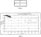
- the stability test diagram of the organic electroluminescent device of Embodiment 1 is shown in FIG. 2 .
- the organic electroluminescent device of Embodiment 1 keeps its brightness above 99.5% thereof during 100 hours of working, which indicates this device has high stability, so it is proved that the cathode metal used by the present invention can form a dense metal film to effectively resist corrosion caused by water and oxygen, thereby preventing the cathode metal layer from being oxidized and thus improving the stability of the device.
- Dynamic service-life experiments (50% alternating checkerboard evaluation) are carried out in a certain work environment, wherein the display screen is lit up in a pattern of alternating checkerboard which changes once every 10 seconds; the service life of the device is evaluated by measuring the brightness decay, and the experiment is stopped when the brightness decays to 50% of the initial brightness, wherein the brightness is measured by using a Spectrascan PR655 photometer.
- the dynamic service life values of the devices of the Embodiments and Comparison examples measured at normal temperature (25°C) are listed in Table 2.
- the electrode provided by the present invention has excellent electron injection capability and stability, and the organic electroluminescent devices produced thereby have a relatively low drive voltage, a relatively high current efficiency and a relatively long service life.
Landscapes
- Physics & Mathematics (AREA)
- Optics & Photonics (AREA)
- Engineering & Computer Science (AREA)
- Manufacturing & Machinery (AREA)
- Electroluminescent Light Sources (AREA)
- Laminated Bodies (AREA)
Abstract
Description
- The present invention pertains to the field of electroluminescence, and particularly relates to an electrode and an organic electroluminescent device using the same.
- An Organic Light-Emitting Diode (OLED) is an active light-emitting device. As compared with Thin-Film-Transistor Liquid Crystal Display (LCD) and Plasma Display Panel (PDP) in the prior art of panel display technologies, organic light-emitting display devices using Organic Light-Emitting Diodes, as one of the technologies that have received the most attention in the panel display technology field, have advantages such as high contrast ratio, wide viewing angle, low power consumption and thinner volume, and are expected to become the next-generation mainstream panel display technology.
- An OLED device mainly comprises an anode, an organic light-emitting layer and a cathode arranged in a stacked manner. In order to increase the electron injection efficiency, the OLED cathode is supposed to use a metal material having its work function that should be as low as possible, and because electrons are more difficult to be injected than holes, the level of work function of the metal seriously affects the light-emitting efficiency and service life of an OLED device, lower work function of the metal may achieve easier electron injection, so as to achieve higher light-emitting efficiency. Besides, lower work function may achieve lower barrier potential of the organics-metal interface, so as to achieve less Joule heat produced during work, thus, the service life of the device may be largely increased.
- However, a single-layered metal cathode with a low work function, such as Mg, Ca, easily becomes oxidized in air, which causes instability of the device and shortens the service life, therefore, an alloy of metal with a low work function and anti-corrosion metal is usually selected to alleviate this problem. When cathode film made of a single metal is evaporation-plated, a lot of morphology defects or structural defects would be formed, which leads to deterioration of the oxidative resistance thereof. When an alloy cathode is evaporation-plated, a small amount of metal having relatively active chemical property would preferentially diffuse into the defects, which makes the film structure more complete, so as to make the entire cathode layer stable.
- However, in actual use, the above-mentioned alloy cathode structure still has relatively poor stability. Research has proven that, the alkali metal forming the cathode's alloy would still reacts with water and oxygen in the air, which lowers the light-emitting efficiency of the device, and in the meantime the alkali metal would easily diffuse into the light-emitting layer and causes quenching of luminescence.
- In view of the above, the present invention provides an electrode having stable performance and an organic electroluminescent device using the same.
- The technical schemes adopted by the present invention are as follows:
The electrode of the present invention comprises a first layer and a second layer arranged in a stacked manner, the first layer is an alkali earth metal alloy layer, and the second layer has a work function of 2.0eV to 3.5eV. - Optionally, the second layer is a lanthanide metal layer and/or a lanthanide metal compound layer.
- Optionally, a lanthanide metal element in the lanthanide metal layer and the lanthanide metal compound layer is Ytterbium and/or Europium.
- Optionally, the first layer is an alkali earth metal alloy layer.
- Optionally, the mass percentage of alkali earth metal in the alkali earth metal alloy layer is 5%-50%.
- Preferably, the mass percentage of alkali earth metal in the alkali earth metal alloy layer is 5%-20%.
- Optionally, the alkali earth metal alloy layer further comprises silver and/or aluminum.
- Optionally, the first layer has a thickness of 0.5nm-30nm.
- Optionally, the second layer has a thickness of 0.5nm-10nm.
- Preferably, the second layer has a thickness of 0.5nm-2nm.
- The organic electroluminescent device of the present invention comprises a first electrode, an organic light-emitting layer and a second electrode arranged in a stacked manner, wherein, the second electrode is the above-mentioned electrode, and the second layer thereof is disposed adjacent to the organic light-emitting layer.
- As compared to the prior art, the above-mentioned technical schemes of the present invention have the following advantages:
- 1. The electrode provided by embodiments of the present invention comprises a first layer and a second layer that are arranged in a stacked manner, the first layer is an alkali earth metal alloy layer, and the second layer has a work function of 2.0eV to 3.5eV. The applicant's research discovered that, such a composite layered electrode with a gradient of work function has very good stability, which can effectively prolong the service life of the device.
- 2. In the electrode provided by embodiments of the present invention, the work function of the second layer is only 2.0eV to 3.5eV, and when the second layer has a thickness of 0.5nm-10nm, it can effectively reduce the barrier potential of the organics-metal interface; in the meantime, the composite electrode structure with a gradient of work function can lower the electron injection barrier potential in a step-by-step manner, thereby providing orderly guidance for electron injection, so that the light-emitting efficiency of the device is improved.
- 3. In the electrode provided by embodiments of the present invention, the second layer is a lanthanide metal layer and/or a lanthanide metal compound layer. Lanthanide metal and lanthanide metal compound not only have relatively low work function, which can effectively lower the electron injection energy barrier and thus lower the drive voltage of the device, but also have relatively low light absorbance, which has relatively small impact on the light out-coupling efficiency. Also, lanthanide metal and lanthanide metal compound have stable chemical property during the evaporation-plating process, which is beneficial for mass production. The first layer is an alkali earth metal alloy layer, wherein the alkali earth metal can effectively prevent the substance in the second layer from dissolving in other cathode materials to form solid solution, which can effectively improve the stability of the electrode and thus improve the stability and service life of the device applying it.
- In order to make the content of the present invention easier to be understood clearly, hereinafter, the present invention is further described in detail according to specific embodiments of the present invention with reference to the accompanying drawings, wherein,
-
FIG. 1 is a structural schematic diagram of the electrode ofEmbodiment 1 of the present invention; -
FIG. 2 is a stability test diagram of the organic electroluminescent device ofEmbodiment 1 of the present invention. - The reference signs in the accompanying drawings represent: 1-first layer, 2-second layer.
- In order to make the objective, technical scheme and advantages of the present invention clearer, detailed description of embodiments of the present invention is further given below, with reference to the accompanying drawings.
- The present invention can be implemented in many different forms and should not be interpreted to be limited to the embodiments described herein. On the contrary, by providing these embodiments, the present disclosure is made complete and thorough, and the inventive concept of the present invention is sufficiently conveyed to those skilled in the art, wherein the present invention is only defined by the claims. In the accompanying drawings, for the sake of clarity, dimensions and relative sizes of layers and areas might be exaggerated.
- This embodiment provides an electrode, as shown in
Figure 1 , the electrode comprises afirst layer 1 and asecond layer 2 arranged in a stacked manner, thefirst layer 1 is an alloy layer of Ag : Mg with a thickness of 13nm. The mass percentage of Mg is 10%. The second layer is Yb layer with a thickness of 1nm. - This embodiment also provides an organic electroluminescent device, Ag/ITO(20nm)/HATCN(20nm)/NPB(40nm)/mCBP: 10wt% Ir(ppy)3(30nm) /TPBi(50nm)/Yb(1nm)/Ag:10% Mg(13nm)/ITO(20nm).
- The first electrode is an Ag layer stacked with an ITO layer.
- The hole injection layer is a HATCN
(2,3,6,7,10,11-hexacyanyl-1,4,5,8,9,12-hexaazatriphenylene) layer. - The hole transport layer is a NPB (N,N'-di-(1-naphthyl)-N,N'-diphenyl-1,1'-biphenyl-4,4'-diamine) layer.
- The light-emitting layer is a layer of CBP (4,4'-di-carbazolyl-biphenyl) doped with Ir(ppy)3 (tri-(2-phenylpyridinyl)-Iridium (III)).
- The hole blocking layer is TPBi (1,3,5-tri-(1-phenyl-1H- benzimidazole-2-yl)-benzene) layer.
- The second electrode is the above-mentioned electrode.
- The optical coupling layer is ITO (Indium Tin Oxide) layer.
- As alternative embodiments of the present invention, the structure of the organic electroluminescent device is not limited to this, as long as it applies the electrode of the present invention and can thereby realize the purpose of the present invention, these alternatives all belong to the protection scope of the present invention.
- As alternative embodiments of the present invention, the material in the second layer is not limited to this, and any lanthanide metal and/or lanthanide metal compound having a work function of 2.0eV to 3.5eV applied therein can realize the purpose of the present invention and belongs to the protection scope of the present invention.
- This embodiment provides an electrode with a structure similar to that of
Embodiment 1, but the difference is that the first layer is Al layer, and the second layer has a thickness of 10nm. - This embodiment also provides an organic electroluminescent device with a structure similar to that of
Embodiment 1, but the difference is that the second electrode is an electrode according to this embodiment. - This embodiment provides an electrode with a structure similar to that of
Embodiment 1, but the difference is that the second layer is Eu layer with a thickness of 0.5nm. - This embodiment also provides an organic electroluminescent device with a structure similar to that of
Embodiment 1, but the difference is that the second electrode is an electrode according to this embodiment. - This embodiment provides an electrode with a structure similar to that of
Embodiment 1, but the difference is that the second layer is Yb2O3 layer, and the first layer has a Mg mass percentage of 5% and a thickness of 0.5nm. - This embodiment also provides an organic electroluminescent device with a structure similar to that of
Embodiment 1, but the difference is that the second electrode is an electrode according to this embodiment. - This embodiment provides an electrode with a structure similar to that of
Embodiment 1, and the difference is: the second layer is a doped layer of YbN and Yb, wherein the mass ratio of YbN:Yb is 1:1; and the first layer is an alloy layer of Ag and Ca with a thickness of 30nm, wherein the mass percentage of Ca is 20%. - This embodiment also provides an organic electroluminescent device with a structure similar to that of
Embodiment 1, but the difference is that the second electrode is an electrode according to this embodiment. - This embodiment provides an electrode with a structure similar to that of
Embodiment 1, and the difference is: the second layer is a doped layer of Yb and Ce2O, wherein the mass ratio of Yb:Ce2O is 1:1. - This embodiment also provides an organic electroluminescent device with a structure similar to that of
Embodiment 1, but the difference is that the second electrode is an electrode according to this embodiment. - This embodiment provides an electrode with a structure similar to that of
Embodiment 1, but the difference is that the first layer has a Mg mass percentage of 50%; and the second layer has a thickness of 2nm. - This embodiment also provides an organic electroluminescent device with a structure similar to that of
Embodiment 1, but the difference is that the second electrode is an electrode according to this embodiment. - This comparison example provides an electrode which is an alloy layer of Ag and Mg with a thickness of 13nm, wherein the mass ratio of Ag : Mg is 10 : 1.
- This comparison example also provides an organic electroluminescent device with a structure similar to that of
Embodiment 1, but the difference is that the second electrode is an electrode according to this comparison example. - This comparison example provides an electrode with a structure similar to that of
Embodiment 1, and the only difference is: the first layer has a Mg mass percentage of 70%. - This comparison example also provides an organic electroluminescent device with a structure similar to that of
Embodiment 1, and the difference is: the second electrode is an electrode according to this comparison example. - This comparison example provides an electrode with a structure similar to that of
Embodiment 1, but the only difference is that the second layer has a thickness of 20nm. - This comparison example also provides an organic electroluminescent device with a structure similar to that of
Embodiment 1, but the difference is that the second electrode is an electrode according to this comparison example. - When an organic electroluminescent device has worked for a long time, the organic films thereof may change from an initial amorphous film into a crystalline film, such a change of film would cause decaying of the device.
- Therefore, the devices are annealed respectively at different temperatures for 1 hour, and the test results of T97 (service time for the brightness of the device to decay from 10000nit to 97% thereof) of the annealed devices as compared to unannealed devices (25°C) are listed in Table 1.
Table 1 Test results of T97 of devices annealed respectively at different temperatures for 1 hour annealing temperature unannealed 80° C 100° C 120° C 140° C T97 (h) T97 (h) T97 (h) T97 (h) T97 (h) Embodiment 1573 553 532 420 375 Embodiment 2521 506 418 321 280 Embodiment 3 550 532 453 398 312 Embodiment 4 567 507 487 425 301 Embodiment 5 503 499 466 304 241 Embodiment 6 515 478 432 263 199 Embodiment 7 570 543 512 401 305 Comparison example 1 496 425 382 257 109 Comparison example 2 501 415 382 217 91 Comparison example 3 454 325 252 147 79 - The data in Table 1 indicates that, when the electrode of the present invention is used in a device, the device's service life is far longer than the service life of the devices provided by the Comparison examples, and in high temperature environment (140° C) it can even be longer than 4 times of the service life of Comparison example 1. Therefore, the electrode of the present invention has excellent high-temperature stability.
- The stability test diagram of the organic electroluminescent device of
Embodiment 1 is shown inFIG. 2 . When testing the OLED device, it is a common way to use high current density testing which utilized a circuit compensation principle. For an ultra-high brightness of 10000nit, the organic electroluminescent device ofEmbodiment 1 keeps its brightness above 99.5% thereof during 100 hours of working, which indicates this device has high stability, so it is proved that the cathode metal used by the present invention can form a dense metal film to effectively resist corrosion caused by water and oxygen, thereby preventing the cathode metal layer from being oxidized and thus improving the stability of the device. - Dynamic service-life experiments (50% alternating checkerboard evaluation) are carried out in a certain work environment, wherein the display screen is lit up in a pattern of alternating checkerboard which changes once every 10 seconds; the service life of the device is evaluated by measuring the brightness decay, and the experiment is stopped when the brightness decays to 50% of the initial brightness, wherein the brightness is measured by using a Spectrascan PR655 photometer. The dynamic service life values of the devices of the Embodiments and Comparison examples measured at normal temperature (25°C) are listed in Table 2.
Table 2 Results of dynamic service-life experiments of devices at normal temperature (25°C) Groups Required brightness (cd/m2) Drive voltage (V) Current efficiency (cd/A) Service life (h) Embodiment 110000 4.34 110 573 Embodiment 210000 5.72 90 521 Embodiment 3 10000 4.89 101 550 Embodiment 4 10000 4.68 105 567 Embodiment 5 10000 5.46 99 503 Embodiment 6 10000 5.84 91 515 Embodiment 7 10000 5.73 97 570 Comparison example 1 10000 5.90 83 496 Comparison example 2 10000 5.82 96 501 Comparison example 3 10000 4.31 102 454 - It can be seen from the test results in Table 2 that, the electrode provided by the present invention has excellent electron injection capability and stability, and the organic electroluminescent devices produced thereby have a relatively low drive voltage, a relatively high current efficiency and a relatively long service life.
- Apparently, the aforementioned embodiments are merely examples illustrated for clearly describing the present invention, rather than limiting the implementation ways thereof. For a person skilled in the art, various changes and modifications in other different forms can be made on the basis of the aforementioned description. It is unnecessary and impossible to exhaustively list all the implementation ways herein. However, any obvious changes or modifications derived from the aforementioned description are intended to be embraced within the protection scope of the present invention.
Claims (10)
- An electrode, comprising a first layer and a second layer arranged in a stacked manner, the first layer is an alkali earth metal alloy layer, and the second layer has a work function of 2.0eV to 3.5eV.
- The electrode according to Claim 1, wherein the second layer is a lanthanide metal layer and/or a lanthanide metal compound layer.
- The electrode according to Claim 2, wherein a lanthanide metal element in the lanthanide metal layer and the lanthanide metal compound layer is Ytterbium and/or Europium.
- The electrode according to Claim 1, wherein the mass percentage of alkali earth metal in the alkali earth metal alloy layer is 5%-50%.
- The electrode according to Claim 4, wherein the mass percentage of alkali earth metal in the alkali earth metal alloy layer is 5%-20%.
- The electrode according to Claim 5, wherein the alkali earth metal alloy layer further comprises silver and/or aluminum.
- The electrode according to any one of Claims 1-6, wherein the first layer has a thickness of 0.5nm-30nm.
- The electrode according to any one of Claims 1-6, wherein the second layer has a thickness of 0.5nm-10nm.
- The electrode according to Claim 8, wherein the second layer has a thickness of 0.5nm-2nm.
- An organic electroluminescent device, comprising a first electrode, an organic light-emitting layer and a second electrode arranged in a stacked manner, wherein, the second electrode is an electrode according to any one of Claims 1-9, and the second layer thereof is disposed adjacent to the organic light-emitting layer.
Applications Claiming Priority (2)
| Application Number | Priority Date | Filing Date | Title |
|---|---|---|---|
| CN201710008675.4A CN108281565A (en) | 2017-01-05 | 2017-01-05 | A kind of electrode and apply its organic electroluminescence device |
| PCT/CN2018/071553 WO2018127127A1 (en) | 2017-01-05 | 2018-01-05 | Electrode and organic electroluminescent component applying same |
Publications (2)
| Publication Number | Publication Date |
|---|---|
| EP3471165A1 true EP3471165A1 (en) | 2019-04-17 |
| EP3471165A4 EP3471165A4 (en) | 2019-12-11 |
Family
ID=62789158
Family Applications (1)
| Application Number | Title | Priority Date | Filing Date |
|---|---|---|---|
| EP18736549.9A Withdrawn EP3471165A4 (en) | 2017-01-05 | 2018-01-05 | ELECTRODE AND ORGANIC ELECTROLUMINESCENT COMPONENT USING THE SAME |
Country Status (7)
| Country | Link |
|---|---|
| US (1) | US10658603B2 (en) |
| EP (1) | EP3471165A4 (en) |
| JP (1) | JP6784842B2 (en) |
| KR (1) | KR102276377B1 (en) |
| CN (1) | CN108281565A (en) |
| TW (1) | TW201826564A (en) |
| WO (1) | WO2018127127A1 (en) |
Cited By (1)
| Publication number | Priority date | Publication date | Assignee | Title |
|---|---|---|---|---|
| CN112928220A (en) * | 2021-01-25 | 2021-06-08 | 中国科学院长春应用化学研究所 | Organic light-emitting diode containing crystalline solid solution as light-emitting layer and application |
Families Citing this family (1)
| Publication number | Priority date | Publication date | Assignee | Title |
|---|---|---|---|---|
| US20220302408A1 (en) * | 2019-08-27 | 2022-09-22 | Oti Lumionics Inc. | Light transmissive electrode for light emitting devices |
Family Cites Families (13)
| Publication number | Priority date | Publication date | Assignee | Title |
|---|---|---|---|---|
| JP3813990B2 (en) * | 1996-09-04 | 2006-08-23 | ケンブリッジ ディスプレイ テクノロジー リミテッド | Organic light emitting device and method for manufacturing the same |
| US6255774B1 (en) | 1996-09-04 | 2001-07-03 | Cambridge Display Technology, Ltd. | Multilayer cathode for organic light-emitting device |
| GB9903251D0 (en) | 1999-02-12 | 1999-04-07 | Cambridge Display Tech Ltd | Opto-electric devices |
| JP2003068470A (en) | 2001-06-15 | 2003-03-07 | Sony Corp | Display element |
| US7429822B2 (en) * | 2003-10-28 | 2008-09-30 | Sharp Kabushiki Kaisha | Organic electroluminescence device having a cathode with a metal layer that includes a first metal and a low work function metal |
| US7270894B2 (en) * | 2004-06-22 | 2007-09-18 | General Electric Company | Metal compound-metal multilayer electrodes for organic electronic devices |
| CN1825662A (en) * | 2006-02-09 | 2006-08-30 | 友达光电股份有限公司 | Organic Electroluminescent Devices |
| KR20100106426A (en) * | 2007-12-28 | 2010-10-01 | 스미또모 가가꾸 가부시키가이샤 | Polymer light-emitting device, method for manufacturing the same and polymer light-emitting display device |
| CN101339976B (en) | 2008-08-07 | 2010-09-08 | 清华大学 | An organic electroluminescent device |
| JP2010062057A (en) | 2008-09-05 | 2010-03-18 | Seiko Epson Corp | Organic electroluminescent device and electronic equipment |
| JP5479009B2 (en) * | 2009-09-24 | 2014-04-23 | キヤノン株式会社 | Organic light emitting device |
| KR101918712B1 (en) * | 2012-08-02 | 2018-11-15 | 삼성디스플레이 주식회사 | Organic light emitting diode device |
| KR101620092B1 (en) | 2014-11-06 | 2016-05-13 | 삼성디스플레이 주식회사 | Organic light emitting device and method for fabrication of the same |
-
2017
- 2017-01-05 CN CN201710008675.4A patent/CN108281565A/en active Pending
-
2018
- 2018-01-05 JP JP2019529907A patent/JP6784842B2/en active Active
- 2018-01-05 WO PCT/CN2018/071553 patent/WO2018127127A1/en not_active Ceased
- 2018-01-05 TW TW107100556A patent/TW201826564A/en unknown
- 2018-01-05 US US16/314,736 patent/US10658603B2/en active Active
- 2018-01-05 KR KR1020197016388A patent/KR102276377B1/en active Active
- 2018-01-05 EP EP18736549.9A patent/EP3471165A4/en not_active Withdrawn
Cited By (2)
| Publication number | Priority date | Publication date | Assignee | Title |
|---|---|---|---|---|
| CN112928220A (en) * | 2021-01-25 | 2021-06-08 | 中国科学院长春应用化学研究所 | Organic light-emitting diode containing crystalline solid solution as light-emitting layer and application |
| CN112928220B (en) * | 2021-01-25 | 2023-08-08 | 中国科学院长春应用化学研究所 | Organic electroluminescent diode containing crystalline solid solution as light-emitting layer and application thereof |
Also Published As
| Publication number | Publication date |
|---|---|
| KR102276377B1 (en) | 2021-07-12 |
| US20190207139A1 (en) | 2019-07-04 |
| CN108281565A (en) | 2018-07-13 |
| JP6784842B2 (en) | 2020-11-11 |
| WO2018127127A1 (en) | 2018-07-12 |
| US10658603B2 (en) | 2020-05-19 |
| TW201826564A (en) | 2018-07-16 |
| EP3471165A4 (en) | 2019-12-11 |
| KR20190079665A (en) | 2019-07-05 |
| JP2020513660A (en) | 2020-05-14 |
Similar Documents
| Publication | Publication Date | Title |
|---|---|---|
| TWI514925B (en) | Organic light emitting device | |
| Kang et al. | Enhancing the electroluminescent properties of organic light-emitting devices using a thin NaCl layer | |
| KR20110032589A (en) | Organic light emitting diode | |
| KR20120049639A (en) | Organic light emitting device | |
| CN102484921A (en) | Organic electroluminescent element | |
| EP3447817B1 (en) | Electrode and organic electroluminescent device using same | |
| CN102239741A (en) | Organic el element and method for manufacturing same | |
| US20120097934A1 (en) | Organic Light Emitting Diode and Method of Fabricating the Same | |
| KR20110027484A (en) | Organic light emitting diode | |
| US10658603B2 (en) | Electrode and an organic electroluminescent device using the same | |
| TWI473315B (en) | Organic light emitting device | |
| TWI220101B (en) | Organic electroluminescence device and fabricating method thereof | |
| KR20240156547A (en) | Organic light emitting display panel | |
| CN108281561B (en) | Electrode and organic electroluminescent device using same | |
| WO2018166026A1 (en) | Oled display device and oled display apparatus | |
| JP3693033B2 (en) | Light emitting device and manufacturing method thereof | |
| KR101900150B1 (en) | Manufacturing method for Organic Light Emitting Diodes comprising a passivation thin film having improved property of protecting devices, and Organic Light Emitting Diodes manufactured thereby | |
| Shin et al. | Optimization of Hole Injection and Transport Layers for High-Performance Quantum-Dot Light-Emitting Diodes | |
| JP5164354B2 (en) | Organic EL device | |
| Chang et al. | High-efficiency red organic light emitting diodes incorporating 1, 3, 5-Tris (1-pyrenyl) benzene as the host material | |
| Tsou et al. | Luminance enhancement of hole-blocking organic light-emitting devices with an inter-layer structure | |
| KR101650780B1 (en) | Light extraction layer for top emitting organic light emitting diode and manufacturing method of thereof | |
| KR20120042051A (en) | Organic light emitting diode device | |
| US20180269425A1 (en) | Oled display element and oled display device | |
| Choo et al. | Enhancement of the lifetime in organic light-emitting devices fabricated utilizing wide-bandgap-impurity-doped emitting layers |
Legal Events
| Date | Code | Title | Description |
|---|---|---|---|
| STAA | Information on the status of an ep patent application or granted ep patent |
Free format text: STATUS: THE INTERNATIONAL PUBLICATION HAS BEEN MADE |
|
| PUAI | Public reference made under article 153(3) epc to a published international application that has entered the european phase |
Free format text: ORIGINAL CODE: 0009012 |
|
| STAA | Information on the status of an ep patent application or granted ep patent |
Free format text: STATUS: REQUEST FOR EXAMINATION WAS MADE |
|
| 17P | Request for examination filed |
Effective date: 20190110 |
|
| AK | Designated contracting states |
Kind code of ref document: A1 Designated state(s): AL AT BE BG CH CY CZ DE DK EE ES FI FR GB GR HR HU IE IS IT LI LT LU LV MC MK MT NL NO PL PT RO RS SE SI SK SM TR |
|
| AX | Request for extension of the european patent |
Extension state: BA ME |
|
| RIN1 | Information on inventor provided before grant (corrected) |
Inventor name: LI, WEIWEI Inventor name: LUO, ZHIZHONG Inventor name: ZHAO, FEI Inventor name: MIN, CHAO |
|
| A4 | Supplementary search report drawn up and despatched |
Effective date: 20191108 |
|
| RIC1 | Information provided on ipc code assigned before grant |
Ipc: H01L 51/52 20060101AFI20191104BHEP |
|
| DAV | Request for validation of the european patent (deleted) | ||
| DAX | Request for extension of the european patent (deleted) | ||
| STAA | Information on the status of an ep patent application or granted ep patent |
Free format text: STATUS: EXAMINATION IS IN PROGRESS |
|
| 17Q | First examination report despatched |
Effective date: 20200713 |
|
| STAA | Information on the status of an ep patent application or granted ep patent |
Free format text: STATUS: THE APPLICATION IS DEEMED TO BE WITHDRAWN |
|
| 18D | Application deemed to be withdrawn |
Effective date: 20201124 |