EP3471163A1 - Oled device, manufacturing method thereof, display panel, and display apparatus - Google Patents
Oled device, manufacturing method thereof, display panel, and display apparatus Download PDFInfo
- Publication number
- EP3471163A1 EP3471163A1 EP17777474.2A EP17777474A EP3471163A1 EP 3471163 A1 EP3471163 A1 EP 3471163A1 EP 17777474 A EP17777474 A EP 17777474A EP 3471163 A1 EP3471163 A1 EP 3471163A1
- Authority
- EP
- European Patent Office
- Prior art keywords
- layer
- organic
- electrode
- oled device
- layers
- Prior art date
- Legal status (The legal status is an assumption and is not a legal conclusion. Google has not performed a legal analysis and makes no representation as to the accuracy of the status listed.)
- Withdrawn
Links
Images


Classifications
-
- H—ELECTRICITY
- H10—SEMICONDUCTOR DEVICES; ELECTRIC SOLID-STATE DEVICES NOT OTHERWISE PROVIDED FOR
- H10K—ORGANIC ELECTRIC SOLID-STATE DEVICES
- H10K50/00—Organic light-emitting devices
- H10K50/10—OLEDs or polymer light-emitting diodes [PLED]
- H10K50/11—OLEDs or polymer light-emitting diodes [PLED] characterised by the electroluminescent [EL] layers
- H10K50/125—OLEDs or polymer light-emitting diodes [PLED] characterised by the electroluminescent [EL] layers specially adapted for multicolour light emission, e.g. for emitting white light
-
- H—ELECTRICITY
- H10—SEMICONDUCTOR DEVICES; ELECTRIC SOLID-STATE DEVICES NOT OTHERWISE PROVIDED FOR
- H10K—ORGANIC ELECTRIC SOLID-STATE DEVICES
- H10K59/00—Integrated devices, or assemblies of multiple devices, comprising at least one organic light-emitting element covered by group H10K50/00
- H10K59/30—Devices specially adapted for multicolour light emission
- H10K59/38—Devices specially adapted for multicolour light emission comprising colour filters or colour changing media [CCM]
-
- H—ELECTRICITY
- H10—SEMICONDUCTOR DEVICES; ELECTRIC SOLID-STATE DEVICES NOT OTHERWISE PROVIDED FOR
- H10K—ORGANIC ELECTRIC SOLID-STATE DEVICES
- H10K50/00—Organic light-emitting devices
- H10K50/80—Constructional details
- H10K50/84—Passivation; Containers; Encapsulations
- H10K50/844—Encapsulations
- H10K50/8445—Encapsulations multilayered coatings having a repetitive structure, e.g. having multiple organic-inorganic bilayers
-
- H—ELECTRICITY
- H10—SEMICONDUCTOR DEVICES; ELECTRIC SOLID-STATE DEVICES NOT OTHERWISE PROVIDED FOR
- H10K—ORGANIC ELECTRIC SOLID-STATE DEVICES
- H10K50/00—Organic light-emitting devices
- H10K50/80—Constructional details
- H10K50/86—Arrangements for improving contrast, e.g. preventing reflection of ambient light
-
- H—ELECTRICITY
- H10—SEMICONDUCTOR DEVICES; ELECTRIC SOLID-STATE DEVICES NOT OTHERWISE PROVIDED FOR
- H10K—ORGANIC ELECTRIC SOLID-STATE DEVICES
- H10K50/00—Organic light-emitting devices
- H10K50/80—Constructional details
- H10K50/86—Arrangements for improving contrast, e.g. preventing reflection of ambient light
- H10K50/865—Arrangements for improving contrast, e.g. preventing reflection of ambient light comprising light absorbing layers, e.g. light-blocking layers
-
- H—ELECTRICITY
- H10—SEMICONDUCTOR DEVICES; ELECTRIC SOLID-STATE DEVICES NOT OTHERWISE PROVIDED FOR
- H10K—ORGANIC ELECTRIC SOLID-STATE DEVICES
- H10K59/00—Integrated devices, or assemblies of multiple devices, comprising at least one organic light-emitting element covered by group H10K50/00
- H10K59/80—Constructional details
- H10K59/87—Passivation; Containers; Encapsulations
- H10K59/873—Encapsulations
- H10K59/8731—Encapsulations multilayered coatings having a repetitive structure, e.g. having multiple organic-inorganic bilayers
-
- H—ELECTRICITY
- H10—SEMICONDUCTOR DEVICES; ELECTRIC SOLID-STATE DEVICES NOT OTHERWISE PROVIDED FOR
- H10K—ORGANIC ELECTRIC SOLID-STATE DEVICES
- H10K59/00—Integrated devices, or assemblies of multiple devices, comprising at least one organic light-emitting element covered by group H10K50/00
- H10K59/80—Constructional details
- H10K59/8791—Arrangements for improving contrast, e.g. preventing reflection of ambient light
- H10K59/8792—Arrangements for improving contrast, e.g. preventing reflection of ambient light comprising light absorbing layers, e.g. black layers
-
- H—ELECTRICITY
- H10—SEMICONDUCTOR DEVICES; ELECTRIC SOLID-STATE DEVICES NOT OTHERWISE PROVIDED FOR
- H10K—ORGANIC ELECTRIC SOLID-STATE DEVICES
- H10K71/00—Manufacture or treatment specially adapted for the organic devices covered by this subclass
Definitions
- the present disclosure relates to display technology, and more specifically, to an OLED device and a manufacturing method thereof, a display panel and a display device.
- OLEDs Organic Light-Emitting Diodes
- the small-to-medium-sized OLEDs have been employed in audio panels and mobile phones as display panels.
- the OLED is expected to be further applied to displays of larger sizes such as mobile products, laptops, monitors, wall-hanging TVs and the like.
- the full-color technology is indispensable and crucial for the OLED.
- the large-sized OLED realizes bottom-emitting function usually by means of the combination of thin-film encapsulation technology with the color filter method (WCF) or the color conversion method (CCM).
- WCF color filter method
- CCM color conversion method
- the aperture ratio of the large-sized OLED bottom-emitting devices adopting the above-mentioned two methods is obviously insufficient.
- the embodiments of the present disclosure provide an OLED and a manufacturing method thereof, a display panel and a display device, which can solve the problem in the prior art of the OLED devices of the large-sized OLED having a low aperture ratio and insufficient thinness.
- the present disclosure aims to provide an OLED device.
- the provided OLED device includes: a first electrode disposed on a substrate; an organic light emitting layer disposed on the first electrode; a second electrode disposed on the organic light emitting layer; a stack of layers disposed on the second electrode.
- the stack of layers comprises at least one inorganic layer and at least one organic layer.
- the at least one inorganic layer and the at least one organic layer are alternately arranged.
- One organic layer of the at least one organic layer includes a color conversion layer.
- the at least one inorganic layer serves as a resist layer
- the at least one organic layer serves as a flattened layer
- the at least one inorganic layer and the at least one organic layer have the same number of layers.
- the at least one inorganic layer serves as a resist layer
- the at least one organic layer serves as a flattened layer
- the difference between the number of the at least one inorganic layer and the at least one organic layer is one.
- the color conversion layer includes conversion areas that are provided with color conversion material and a black matrix BM that is provided among the color conversion areas.
- the conversion areas include red conversion areas, green conversion areas and keeping areas which are arranged alternately, and the organic light emitting layer includes blue light emitting material, the red conversion area is configured to convert the incident blue light to red light, the green conversion area is configured to convert the incident blue light to green light, and the keeping area is configured to keep the incident blue light being still blue light.
- the layer that is the most adjacent to the organic light emitting layer in the stack of layers is an inorganic layer.
- the color conversion material includes organic resins.
- the present disclosure also aims to provide a display panel.
- the second aspect of the present disclosure provides a display panel including the above OLED device.
- the present disclosure also aims to provide a display device.
- the third aspect of the present disclosure provides a display device including the above display panel.
- the present disclosure also aims to provide a method of manufacturing an OLED device.
- the four aspect of the present disclosure provides a method of manufacturing an OLED device including: forming a first electrode on a substrate; forming an organic light emitting layer on the first electrode; forming a second electrode on the organic light emitting layer; forming a stack of layers on the second electrode, wherein the stack of layers includes at least one organic layer and at least one inorganic layer, the at least one organic layer and the at least one inorganic layer are alternately arranged, and the method includes configuring an organic layer of the at least one organic layer to include a color conversion layer.
- the at least one inorganic layer serves as a resist layer
- the at least one organic layer serves as a flattened layer.
- the method includes making the at least one inorganic layer and the at least one organic layer have the same number of layers.
- the at least one inorganic layer serves as a resist layer
- the at least one organic layer serves as a flattened layer.
- the method includes making the numbers of the at least one inorganic layer and the at least one organic layer have a difference of one.
- the color conversion layer may include conversion areas that are provided with conversion material, and forming the color conversion layer further includes forming a black matrix among the conversion areas.
- forming the conversion areas includes forming red conversion areas, green conversion areas and keeping areas which are arranged alternately.
- the organic light emitting layer includes blue light emitting material, the red conversion area is configured to convert the incident blue light to red light, the green conversion area is configured to convert the incident blue light to green light, and the keeping area is configured to keep the incident blue light being still blue light.
- the layer that is the most adjacent to the organic light emitting layer in the stack of layers is an inorganic layer.
- the color conversion material includes organic resins.
- the terms “up”, “down”, “left”, “right”, “vertical”, “horizontal”, “top”, “bottom” and their derivative words should concern the present disclosure.
- the terms “over”, “on the top of”, “disposed on” or “disposed on the top of” means that a first element such as a first structure is arranged on a second element such as a second structure, wherein a medium element such as an interface structure may exist between the first element and the second element.
- the term “contact” means a first element such as a first structure and a second element such as a second structure are connected with or without other elements at the interface of the above two elements.
- the provided OLED device includes: a first electrode disposed on a substrate; an organic light emitting layer disposed on the first electrode; a second electrode disposed on the organic light emitting layer; a stack of layers disposed on the second electrode.
- the stack of layers includes at least one inorganic layer and at least one organic layer.
- the at least one inorganic layer and at least one organic layer are alternately arranged.
- One organic layer of the at least one organic layer includes a color conversion layer.
- the stack of layers serves as an encapsulation layer.
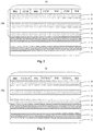
- Fig. 1 schematically illustrates OLED devices according to different embodiments of the present disclosure.
- Fig. 1(a) shows a case where the at least one inorganic layer and the at least one organic layer have the same number of layers.
- the OLED device includes: a substrate 1; a first electrode 2 disposed on the substrate; an organic light emitting layer 3 disposed on the first electrode; a second electrode 4 disposed on the organic light-emitting layer; and a stack of layers 100 disposed on the second electrode.
- the stack of layers 100 includes an inorganic layer 5, an organic layer 6, an inorganic layer 7, an organic layer 8, an inorganic layer 9 and an organic layer 10 which are arranged alternately. Any one of the organic layer 6, the organic layer 8 and the organic layer 10 may include a color conversion layer.
- the organic layer 6, the organic layer 8 and the organic layer 10 are arranged including a color conversion layer.
- the case where only one organic layer includes a color conversion layer is taken as an example to describe the present invention. It is noted that the case where the stack of layers include three inorganic layers and three organic layers is only taken as an example.
- the number of the inorganic layers is not limited to three and may be any desired number, and the number of the inorganic layers is not limited to three and may be any desired number.
- Fig. 1(b) shows a case where the difference between the number of the at least one inorganic layer and the at least one organic layer is one.
- the OLED device includes: a substrate 1; a first electrode 2 disposed on the substrate; an organic light emitting layer 3 disposed on the first electrode; a second electrode 4 disposed on the organic light-emitting layer; and a stack of layers 100' disposed on the second electrode.
- the stack of layers 100' includes an organic layer 6', an inorganic layer 7', an organic layer 8' which are arranged alternately. Any one of the organic layer 6' and the organic layer 8' may include a color conversion layer.
- both of the organic layer 6' and the organic layer 8' may be configured to include a color conversion layer as required.
- the case where only one organic layer includes a color conversion layer is taken as an example to describe the present invention. It is noted the case where the stack of layers include one inorganic layer and two organic layers is only taken as an example.
- the number of the organic layers is not limited to two and may be any desired number, and the number of the inorganic layer is not limited to one and may be any desired number.
- each one of the at least one stack of layers has an inorganic layer(s) and an organic layer(s) which are arranged in order in the direction perpendicular to the upper surface of the substrate, and the organic layer(s) of one stack of layers of the at least one stack of layers is formed as color conversion layer(s).
- Fig. 2 schematically illustrates an OLED device according to one embodiment of the present disclosure.
- Fig. 2 further illustrates more details of Fig. 1(a) .
- the layer that is the most adjacent to the organic light emitting layer in the stack of layers is an inorganic layer.
- the inorganic layer 5, the inorganic layer 7, and the inorganic layer 9 serve as resist layers to block water vapor and air.
- the resist layer includes transparent inorganic materials (e.g., oxides, fluorides, nitrides), or any other materials suitable for blocking water and oxygen.
- the organic layer servers as a flattened layer so as to reduce the stress of the inorganic layer and provide excellent particle-coating effect.
- the flattened layer includes polymer films or any other materials suitable for forming the flattened layer.
- the encapsulation performance of the device can be regulated by adjusting the number and the composition of the resist layer and the flattened layer.
- the substrate may be a rigid substrate or a flexible substrate, which include any materials suitable for forming a substrate, such as high-molecular polymers, metal foils, ultra-thin glasses and the like.
- the first electrode and the second electrode include but are not limited to metals, conductive oxygen compounds, conductive organic molecules, conductive polymers, and/or combinations thereof.
- the color conversion material in the color conversion layer may include organic resins.
- the organic layer 10 includes a color conversion layer.
- the color conversion layer includes conversion areas CCM that are provided with color conversion material and a black matrix BM that is provided among the color conversion areas CCM. It is noted that, the numbers of the conversion areas CCM and the black matrix BM are not limited to the numbers shown in the drawings.
- Fig. 3 further schematically illustrates an OLED device according to one embodiment of the present disclosure.
- the conversion areas CCM include a red conversion area CCM-R, a green conversion area CCM-R and a keeping area CCM-0.
- the organic light emitting layer 3 include blue light emitting material.
- the red conversion area CCM-R is configured to convert the incident blue light to red light
- the green conversion area CCM-G is configured to convert the incident blue light to green light
- the keeping area is configured to keep the incident blue light being still blue light.
- Fig. 4 is a flow chart showing a manufacturing method of an OLED device according to one embodiment of the present disclosure.
- a method of manufacturing the OLED device includes:
- the inorganic layer serves as a resist layer
- the organic layer serves as a flattened layer. This method includes making the at least one inorganic layer and the at least one organic layer have the same number.
- the inorganic layer serves as a resist layer
- the organic layer serves as a flattened layer. This method includes making the numbers of the at least one inorganic layer and the at least one organic layer have a difference of one.
- the color conversion layer may include conversion areas that are provided with conversion material, and forming the color conversion layer further includes forming a black matrix among the conversion areas.
- Forming conversion areas includes forming red conversion areas, green conversion areas and keeping areas which are arranged alternately.
- the organic light emitting layer includes blue light emitting material.
- the red conversion area is configured to convert the incident blue light to red light
- the green conversion area is configured to convert the incident blue light to green light
- the keeping area is configured to keep the incident blue light being still blue light.
- the layer that is the most adjacent to the organic light emitting layer in the stack of layers is an inorganic layer.
- the color conversion material may include organic resins.
- the display panel of embodiments of the present disclosure includes the above OLED device.
- the display device of embodiments of the present disclosure includes the above display panel.
- the display device may be devices having a display function such as display panels, displays, television sets, tablet computers, mobile phones, navigators, etc., which is not limited in the present disclosure.
- the materials of the conversion area, the keeping area, and the black matrix may have the same organic material as the organic layer, such that they can realize a color conversion function while replacing the organic layer in the conventional encapsulation stack of layers consisting of organic layers and inorganic layers. Therefore, as compared with the conventional bottom emitting device, the top emitting device provided in the embodiments of the present disclosure can improve the aperture ratio. Moreover, since the organic layer including the color conversion layer is adopted to replace the organic layer in the conventional encapsulation stack of layers, the device is thinner, the production process is simplified, the manufacturing cost is reduced, and the structure of the obtained device is made more compact.
- the organic layer of one of the at least one of the stack of layers includes the color conversion layer
- the organic layer of one of the at least one of the stack of layers includes the color conversion layer
- the solution that two or more organic layers include the color conversion layer also falls within the scope of the present disclosure.
Landscapes
- Chemical & Material Sciences (AREA)
- Inorganic Chemistry (AREA)
- Physics & Mathematics (AREA)
- Optics & Photonics (AREA)
- Engineering & Computer Science (AREA)
- Manufacturing & Machinery (AREA)
- Electroluminescent Light Sources (AREA)
- Devices For Indicating Variable Information By Combining Individual Elements (AREA)
- Optical Filters (AREA)
Abstract
Description
- The present application claims the priority of Chinese patent application No.
201610402307.3 filed on June 8, 2016 - The present disclosure relates to display technology, and more specifically, to an OLED device and a manufacturing method thereof, a display panel and a display device.
- With the rise in customer demand for audio and video products, there is a growing requirement for the production of high-resolution, high-quality displays. The Organic Light-Emitting Diodes (OLEDs) are considered to be the star product of the next-generation display due to their characteristics such as self-emission, high brightness, wide viewing angle, fast reaction and manufacturable R, G and B full-color components.
- In the current market, the small-to-medium-sized OLEDs have been employed in audio panels and mobile phones as display panels. In the future, the OLED is expected to be further applied to displays of larger sizes such as mobile products, laptops, monitors, wall-hanging TVs and the like. The full-color technology is indispensable and crucial for the OLED.
- The large-sized OLED realizes bottom-emitting function usually by means of the combination of thin-film encapsulation technology with the color filter method (WCF) or the color conversion method (CCM). However, the aperture ratio of the large-sized OLED bottom-emitting devices adopting the above-mentioned two methods is obviously insufficient.
- The embodiments of the present disclosure provide an OLED and a manufacturing method thereof, a display panel and a display device, which can solve the problem in the prior art of the OLED devices of the large-sized OLED having a low aperture ratio and insufficient thinness.
- The present disclosure aims to provide an OLED device.
- In one embodiment of the present disclosure, the provided OLED device includes: a first electrode disposed on a substrate; an organic light emitting layer disposed on the first electrode; a second electrode disposed on the organic light emitting layer; a stack of layers disposed on the second electrode. The stack of layers comprises at least one inorganic layer and at least one organic layer. The at least one inorganic layer and the at least one organic layer are alternately arranged. One organic layer of the at least one organic layer includes a color conversion layer.
- In one embodiment, the at least one inorganic layer serves as a resist layer, the at least one organic layer serves as a flattened layer, and the at least one inorganic layer and the at least one organic layer have the same number of layers.
- In one embodiment, the at least one inorganic layer serves as a resist layer, the at least one organic layer serves as a flattened layer, and the difference between the number of the at least one inorganic layer and the at least one organic layer is one.
- In one embodiment, the color conversion layer includes conversion areas that are provided with color conversion material and a black matrix BM that is provided among the color conversion areas.
- In one embodiment, the conversion areas include red conversion areas, green conversion areas and keeping areas which are arranged alternately, and the organic light emitting layer includes blue light emitting material, the red conversion area is configured to convert the incident blue light to red light, the green conversion area is configured to convert the incident blue light to green light, and the keeping area is configured to keep the incident blue light being still blue light.
- In one embodiment, the layer that is the most adjacent to the organic light emitting layer in the stack of layers is an inorganic layer.
- In one embodiment, the color conversion material includes organic resins.
- The present disclosure also aims to provide a display panel.
- The second aspect of the present disclosure provides a display panel including the above OLED device.
- The present disclosure also aims to provide a display device.
- The third aspect of the present disclosure provides a display device including the above display panel.
- The present disclosure also aims to provide a method of manufacturing an OLED device.
- The four aspect of the present disclosure provides a method of manufacturing an OLED device including: forming a first electrode on a substrate; forming an organic light emitting layer on the first electrode; forming a second electrode on the organic light emitting layer; forming a stack of layers on the second electrode, wherein the stack of layers includes at least one organic layer and at least one inorganic layer, the at least one organic layer and the at least one inorganic layer are alternately arranged, and the method includes configuring an organic layer of the at least one organic layer to include a color conversion layer.
- In one embodiment, the at least one inorganic layer serves as a resist layer, the at least one organic layer serves as a flattened layer. The method includes making the at least one inorganic layer and the at least one organic layer have the same number of layers.
- In one embodiment, the at least one inorganic layer serves as a resist layer, the at least one organic layer serves as a flattened layer. The method includes making the numbers of the at least one inorganic layer and the at least one organic layer have a difference of one.
- In one embodiment, the color conversion layer may include conversion areas that are provided with conversion material, and forming the color conversion layer further includes forming a black matrix among the conversion areas.
- In one embodiment, forming the conversion areas includes forming red conversion areas, green conversion areas and keeping areas which are arranged alternately. The organic light emitting layer includes blue light emitting material, the red conversion area is configured to convert the incident blue light to red light, the green conversion area is configured to convert the incident blue light to green light, and the keeping area is configured to keep the incident blue light being still blue light.
- In one embodiment, the layer that is the most adjacent to the organic light emitting layer in the stack of layers is an inorganic layer.
- In one embodiment, the color conversion material includes organic resins.
- In order to further clarify the technical solutions of the embodiments of the present disclosure, the drawings of the embodiments will be briefly described below. It should be understood that the drawings described below relate only to some embodiments of the present disclosure and are not limitative to the present disclosure.
-
Fig. 1(a) schematically illustrates a configuration of an OLED device according to one embodiment of the present disclosure; -
Fig. 1(b) schematically illustrates a configuration of an OLED device according to one embodiment of the present disclosure; -
Fig. 2 schematically illustrates a configuration of an OLED device according to one embodiment of the present disclosure; -
Fig. 3 schematically illustrates a configuration of an OLED device according to one embodiment of the present disclosure; -
Fig. 4 is a flow chart showing a manufacturing method of an OLED device according to one embodiment of the present disclosure. - In order to make the purpose, technical solutions and advantages of the embodiments of the present disclosure clearer, the technical solution of the embodiments of the present disclosure will be described clearly and completely below in conjunction with the accompanying drawings. It is obvious that the described embodiments are a part of the embodiments of the present disclosure but not all the embodiment of the present disclosure. Based on the described embodiments of the present disclosure, those skilled in the art can obtain other embodiments, without any inventive work, which should fall within the scope of the invention.
- When the elements of the present disclosure and their embodiments are described, the singular form of the word used in the present disclosure the appended claims includes the plural form, and vice versa, unless otherwise explicitly specified in the context. Therefore, when referring to a term with a singular form, the plural form of this term is usually included. The terms "comprise", "include", "contain", "have" are intended to be inclusive and to indicate that there may be additional elements other than the listed elements.
- For the purposes of describing surfaces below, as the indicated directions in the drawings, the terms "up", "down", "left", "right", "vertical", "horizontal", "top", "bottom" and their derivative words should concern the present disclosure. The terms "over", "on the top of", "disposed on" or "disposed on the top of" means that a first element such as a first structure is arranged on a second element such as a second structure, wherein a medium element such as an interface structure may exist between the first element and the second element. The term "contact" means a first element such as a first structure and a second element such as a second structure are connected with or without other elements at the interface of the above two elements.
- In one embodiment of the present disclosure, the provided OLED device includes: a first electrode disposed on a substrate; an organic light emitting layer disposed on the first electrode; a second electrode disposed on the organic light emitting layer; a stack of layers disposed on the second electrode. The stack of layers includes at least one inorganic layer and at least one organic layer. The at least one inorganic layer and at least one organic layer are alternately arranged. One organic layer of the at least one organic layer includes a color conversion layer. The stack of layers serves as an encapsulation layer.
-
Fig. 1 schematically illustrates OLED devices according to different embodiments of the present disclosure. -
Fig. 1(a) shows a case where the at least one inorganic layer and the at least one organic layer have the same number of layers. As shown inFig. 1(a) , the OLED device includes: asubstrate 1; afirst electrode 2 disposed on the substrate; an organiclight emitting layer 3 disposed on the first electrode; asecond electrode 4 disposed on the organic light-emitting layer; and a stack oflayers 100 disposed on the second electrode. The stack oflayers 100 includes aninorganic layer 5, anorganic layer 6, aninorganic layer 7, anorganic layer 8, aninorganic layer 9 and anorganic layer 10 which are arranged alternately. Any one of theorganic layer 6, theorganic layer 8 and theorganic layer 10 may include a color conversion layer. However, at least one of theorganic layer 6, theorganic layer 8 and theorganic layer 10 are arranged including a color conversion layer. The case where only one organic layer includes a color conversion layer is taken as an example to describe the present invention. It is noted that the case where the stack of layers include three inorganic layers and three organic layers is only taken as an example. The number of the inorganic layers is not limited to three and may be any desired number, and the number of the inorganic layers is not limited to three and may be any desired number. -
Fig. 1(b) shows a case where the difference between the number of the at least one inorganic layer and the at least one organic layer is one. As shown inFig. 1(b) , the OLED device includes: asubstrate 1; afirst electrode 2 disposed on the substrate; an organiclight emitting layer 3 disposed on the first electrode; asecond electrode 4 disposed on the organic light-emitting layer; and a stack of layers 100' disposed on the second electrode. The stack of layers 100' includes an organic layer 6', an inorganic layer 7', an organic layer 8' which are arranged alternately. Any one of the organic layer 6' and the organic layer 8' may include a color conversion layer. However, both of the organic layer 6' and the organic layer 8' may be configured to include a color conversion layer as required. The case where only one organic layer includes a color conversion layer is taken as an example to describe the present invention. It is noted the case where the stack of layers include one inorganic layer and two organic layers is only taken as an example. The number of the organic layers is not limited to two and may be any desired number, and the number of the inorganic layer is not limited to one and may be any desired number. - It is possible to effectively increase the aperture ratio of the OLED device while making the device thinner, simplifying the process, reducing the manufacturing cost, and making the structure of the obtained device more compact through the following steps: forming a first electrode on a substrate; forming an organic light emitting layer on the first electrode; forming a second electrode on the organic light emitting layer; forming at least one stack of layers on the second electrode, wherein each one of the at least one stack of layers has an inorganic layer(s) and an organic layer(s) which are arranged in order in the direction perpendicular to the upper surface of the substrate, and the organic layer(s) of one stack of layers of the at least one stack of layers is formed as color conversion layer(s).
- In the following section, as an example, the case where the number of both the at least one inorganic layer and the at least one organic layer are three is described for illustrative purposes.
-
Fig. 2 schematically illustrates an OLED device according to one embodiment of the present disclosure.Fig. 2 further illustrates more details ofFig. 1(a) . In the configuration shown inFig. 2 , the layer that is the most adjacent to the organic light emitting layer in the stack of layers is an inorganic layer. Theinorganic layer 5, theinorganic layer 7, and theinorganic layer 9 serve as resist layers to block water vapor and air. The resist layer includes transparent inorganic materials (e.g., oxides, fluorides, nitrides), or any other materials suitable for blocking water and oxygen. The organic layer servers as a flattened layer so as to reduce the stress of the inorganic layer and provide excellent particle-coating effect. The flattened layer includes polymer films or any other materials suitable for forming the flattened layer. The encapsulation performance of the device can be regulated by adjusting the number and the composition of the resist layer and the flattened layer. - The substrate may be a rigid substrate or a flexible substrate, which include any materials suitable for forming a substrate, such as high-molecular polymers, metal foils, ultra-thin glasses and the like. The first electrode and the second electrode include but are not limited to metals, conductive oxygen compounds, conductive organic molecules, conductive polymers, and/or combinations thereof. The color conversion material in the color conversion layer may include organic resins.
- In the embodiment shown in
Fig. 2 , theorganic layer 10 includes a color conversion layer. As can be seen fromFig. 2 , the color conversion layer includes conversion areas CCM that are provided with color conversion material and a black matrix BM that is provided among the color conversion areas CCM. It is noted that, the numbers of the conversion areas CCM and the black matrix BM are not limited to the numbers shown in the drawings. -
Fig. 3 further schematically illustrates an OLED device according to one embodiment of the present disclosure. As shown inFig. 3 , the conversion areas CCM include a red conversion area CCM-R, a green conversion area CCM-R and a keeping area CCM-0. The organiclight emitting layer 3 include blue light emitting material. The red conversion area CCM-R is configured to convert the incident blue light to red light, the green conversion area CCM-G is configured to convert the incident blue light to green light, and the keeping area is configured to keep the incident blue light being still blue light. -
Fig. 4 is a flow chart showing a manufacturing method of an OLED device according to one embodiment of the present disclosure. In one embodiment, a method of manufacturing the OLED device includes: - S1. forming a first electrode, i.e., forming a first electrode on a substrate;
- S2. forming an organic light emitting layer, i.e., forming an organic light emitting layer on the first electrode;
- S3. forming a second electrode, i.e., forming a second electrode on the organic light emitting layer;
- S4. forming a stack of layers having a color conversion layer, i.e., forming on the second electrode at least one stack of layers which has at least one organic layer and at least one inorganic layer, wherein the at least one organic layer and the at least one inorganic layer are arranged alternately, and this S4 further includes that one organic layer of the at least one organic layer is configured to include a color conversion layer.
- In one embodiment, the inorganic layer serves as a resist layer, the organic layer serves as a flattened layer. This method includes making the at least one inorganic layer and the at least one organic layer have the same number.
- In one embodiment, the inorganic layer serves as a resist layer, the organic layer serves as a flattened layer. This method includes making the numbers of the at least one inorganic layer and the at least one organic layer have a difference of one.
- The color conversion layer may include conversion areas that are provided with conversion material, and forming the color conversion layer further includes forming a black matrix among the conversion areas.
- Forming conversion areas includes forming red conversion areas, green conversion areas and keeping areas which are arranged alternately. The organic light emitting layer includes blue light emitting material. The red conversion area is configured to convert the incident blue light to red light, the green conversion area is configured to convert the incident blue light to green light, and the keeping area is configured to keep the incident blue light being still blue light.
- In one embodiment, the layer that is the most adjacent to the organic light emitting layer in the stack of layers is an inorganic layer. The color conversion material may include organic resins.
- The display panel of embodiments of the present disclosure includes the above OLED device. The display device of embodiments of the present disclosure includes the above display panel. The display device may be devices having a display function such as display panels, displays, television sets, tablet computers, mobile phones, navigators, etc., which is not limited in the present disclosure.
- In the embodiments of the present disclosure, the materials of the conversion area, the keeping area, and the black matrix may have the same organic material as the organic layer, such that they can realize a color conversion function while replacing the organic layer in the conventional encapsulation stack of layers consisting of organic layers and inorganic layers. Therefore, as compared with the conventional bottom emitting device, the top emitting device provided in the embodiments of the present disclosure can improve the aperture ratio. Moreover, since the organic layer including the color conversion layer is adopted to replace the organic layer in the conventional encapsulation stack of layers, the device is thinner, the production process is simplified, the manufacturing cost is reduced, and the structure of the obtained device is made more compact.
- It is noted that, "the organic layer of one of the at least one of the stack of layers includes the color conversion layer" recited in the present disclosure is not intended to limit the number of the organic layer having the color conversion layer to one. The solution that two or more organic layers include the color conversion layer also falls within the scope of the present disclosure.
- Particular embodiments have been described above. These embodiments are presented by way of example only and are not intended to limit the scope of the present disclosure. In fact, the novel embodiments described herein may be embodied in various other forms. Additionally, various omissions, substitutions and modifications in the form of embodiments described herein may be made without departing from the spirit of the present disclosure. The appended claims and their equivalents are intended to cover such forms or modifications that fall within the scope of the spirit of the present disclosure.
Claims (10)
- An OLED device comprising: a first electrode disposed on a substrate; an organic light emitting layer disposed on the first electrode; a second electrode disposed on the organic light emitting layer; a stack of layers disposed on the second electrode, wherein the stack of layers comprises at least one inorganic layer and at least one organic layer, the at least one inorganic layer and the at least one organic layer are alternately arranged,
and an organic layer of the at least one organic layer comprises a color conversion layer. - The OLED device according to claim 1, wherein the at least one inorganic layer serves as a resist layer, the at least one organic layer serves as a flattened layer, and the at least one inorganic layer and the at least one organic layer have the same number of layers.
- The OLED device according to claim 1, wherein the at least one inorganic layer serves as a resist layer, the at least one organic layer serves as a flattened layer, and a difference between the number of the at least one inorganic layer and the at least one organic layer is one.
- The OLED device according to claim 2 or 3, wherein the color conversion layer comprises conversion areas that are provided with color conversion material and a black matrix that is provided among the color conversion areas.
- The OLED device according to claim 4, wherein the conversion areas comprise red conversion areas, green conversion areas and keeping areas which are arranged alternately, and the organic light emitting layer comprises blue light emitting material, the red conversion area is configured to convert the incident blue light to red light, the green conversion area is configured to convert the incident blue light to green light, and the keeping area is configured to keep the incident blue light being still blue light.
- The OLED device according to claim 2, wherein the layer that is the most adjacent to the organic light emitting layer in the stack of layers is an inorganic layer.
- The OLED device according to any one of claims 1-3, wherein the color conversion material comprises organic resin.
- A display panel comprising the OLED device according to any one of claims 1-7.
- A display device comprising the display panel according to claim 8.
- A method of manufacturing an OLED device comprising: forming a first electrode on a substrate; forming an organic light emitting layer on the first electrode; forming a second electrode on the organic light emitting layer; forming a stack of layers on the second electrode, wherein the stack of layers comprises at least one organic layer and at least one inorganic layer, the at least one organic layer and the at least one inorganic layer are alternately arranged,
and the method comprises configuring an organic layer of the at least one organic layer to comprise a color conversion layer.
Applications Claiming Priority (2)
| Application Number | Priority Date | Filing Date | Title |
|---|---|---|---|
| CN201610402307.3A CN105932169A (en) | 2016-06-08 | 2016-06-08 | OLED (Organic Light Emitting Diode) device and manufacturing method thereof, display panel and display device |
| PCT/CN2017/083045 WO2017211148A1 (en) | 2016-06-08 | 2017-05-04 | Oled device, manufacturing method thereof, display panel, and display apparatus |
Publications (2)
| Publication Number | Publication Date |
|---|---|
| EP3471163A1 true EP3471163A1 (en) | 2019-04-17 |
| EP3471163A4 EP3471163A4 (en) | 2020-03-04 |
Family
ID=56833759
Family Applications (1)
| Application Number | Title | Priority Date | Filing Date |
|---|---|---|---|
| EP17777474.2A Withdrawn EP3471163A4 (en) | 2016-06-08 | 2017-05-04 | OLED DEVICE, MANUFACTURING METHOD THEREFOR, DISPLAY PANEL AND DISPLAY DEVICE |
Country Status (5)
| Country | Link |
|---|---|
| US (1) | US10355056B2 (en) |
| EP (1) | EP3471163A4 (en) |
| JP (1) | JP2018525767A (en) |
| CN (1) | CN105932169A (en) |
| WO (1) | WO2017211148A1 (en) |
Families Citing this family (3)
| Publication number | Priority date | Publication date | Assignee | Title |
|---|---|---|---|---|
| CN105932169A (en) | 2016-06-08 | 2016-09-07 | 京东方科技集团股份有限公司 | OLED (Organic Light Emitting Diode) device and manufacturing method thereof, display panel and display device |
| CN111162200A (en) | 2020-01-03 | 2020-05-15 | 武汉天马微电子有限公司 | Display panel and display device |
| CN111864107A (en) * | 2020-07-10 | 2020-10-30 | 武汉华星光电半导体显示技术有限公司 | TFT array substrate, display device and preparation method of TFT array substrate |
Family Cites Families (20)
| Publication number | Priority date | Publication date | Assignee | Title |
|---|---|---|---|---|
| KR100426964B1 (en) | 2002-03-20 | 2004-04-13 | 엘지.필립스 엘시디 주식회사 | Organic Electroluminescent Device and Method for Fabricating the same |
| KR20050029426A (en) * | 2003-09-22 | 2005-03-28 | 삼성에스디아이 주식회사 | Full color oled having color filter layer or color conversion medium |
| KR100581775B1 (en) | 2003-12-30 | 2006-05-23 | 엘지.필립스 엘시디 주식회사 | Organic electroluminescent device and manufacturing method thereof |
| JP2006073219A (en) | 2004-08-31 | 2006-03-16 | Sony Corp | Display device and manufacturing method thereof |
| CN101305643B (en) | 2005-11-11 | 2010-05-19 | 富士电机控股株式会社 | Organic el light emitting display |
| US8174187B2 (en) * | 2007-01-15 | 2012-05-08 | Global Oled Technology Llc | Light-emitting device having improved light output |
| KR100882668B1 (en) * | 2007-07-18 | 2009-02-06 | 삼성모바일디스플레이주식회사 | Organic light emitting display device and manufacturing method thereof |
| JP5162179B2 (en) | 2007-07-31 | 2013-03-13 | 住友化学株式会社 | LIGHT EMITTING ELEMENT, MANUFACTURING METHOD THEREOF, AND LIGHTING DEVICE |
| KR101372851B1 (en) | 2008-07-11 | 2014-03-12 | 삼성디스플레이 주식회사 | Organic light emitting display apparatus |
| JP5214360B2 (en) | 2008-07-29 | 2013-06-19 | シャープ株式会社 | Color conversion organic EL display |
| JP5081324B2 (en) * | 2012-01-25 | 2012-11-28 | 住友化学株式会社 | Active matrix substrate, display panel, display device, and transistor element |
| CN102998734B (en) | 2012-11-19 | 2016-03-23 | 京东方科技集团股份有限公司 | Graphical delayer and manufacture method, display device |
| KR102080008B1 (en) * | 2013-07-12 | 2020-02-24 | 삼성디스플레이 주식회사 | Organic luminescence emitting display device and method for manufacturing the same |
| CN104752620A (en) | 2013-12-26 | 2015-07-01 | 业鑫科技顾问股份有限公司 | Color conversion layer, organic electroluminescence display panel and liquid crystal display panel |
| KR20160011765A (en) * | 2014-07-22 | 2016-02-02 | 삼성디스플레이 주식회사 | Display Device |
| KR20160036722A (en) * | 2014-09-25 | 2016-04-05 | 삼성디스플레이 주식회사 | organic light emitting diode display and manufacturing method thereof |
| KR102356841B1 (en) * | 2014-11-21 | 2022-02-03 | 삼성디스플레이 주식회사 | Organic light emitting display device and method of manufacturing the same |
| CN105394674A (en) | 2015-11-06 | 2016-03-16 | 芜湖市好亦快食品有限公司三山分公司 | Blood-supplementing and eyesight-improving sesame lotus root jelly and preparation method thereof |
| KR102586049B1 (en) * | 2015-11-13 | 2023-10-10 | 삼성디스플레이 주식회사 | Mask frame assembly, apparatus for manufacturing display apparatus and method of manufacturing display apparatus |
| CN105932169A (en) | 2016-06-08 | 2016-09-07 | 京东方科技集团股份有限公司 | OLED (Organic Light Emitting Diode) device and manufacturing method thereof, display panel and display device |
-
2016
- 2016-06-08 CN CN201610402307.3A patent/CN105932169A/en active Pending
-
2017
- 2017-05-04 JP JP2017553353A patent/JP2018525767A/en active Pending
- 2017-05-04 US US15/564,084 patent/US10355056B2/en active Active
- 2017-05-04 WO PCT/CN2017/083045 patent/WO2017211148A1/en not_active Ceased
- 2017-05-04 EP EP17777474.2A patent/EP3471163A4/en not_active Withdrawn
Also Published As
| Publication number | Publication date |
|---|---|
| WO2017211148A1 (en) | 2017-12-14 |
| US20180197920A1 (en) | 2018-07-12 |
| JP2018525767A (en) | 2018-09-06 |
| US10355056B2 (en) | 2019-07-16 |
| CN105932169A (en) | 2016-09-07 |
| EP3471163A4 (en) | 2020-03-04 |
Similar Documents
| Publication | Publication Date | Title |
|---|---|---|
| US9773994B2 (en) | Organic light-emitting diode display for suppressing organic light-emitting element from being damaged | |
| EP3270434B1 (en) | Top-emitting organic electroluminescent display panel, manufacturing method thereof and display device | |
| US10930896B2 (en) | Package method of OLED element and OLED package structure | |
| US11139453B2 (en) | Flexible display panel having blocking walls | |
| US11508933B2 (en) | Display panel and display device | |
| US12150363B2 (en) | Display panel, display screen and display device having larger viewing angle | |
| WO2019233479A1 (en) | Display panel and display device | |
| US11075360B2 (en) | Display panel, display device and method for manufacturing display panel | |
| CN112164709A (en) | Organic light emitting diode display panel, preparation method thereof and display device | |
| JP6014340B2 (en) | Display device | |
| CN103926722B (en) | A kind of manufacture method of display floater, display device and display floater | |
| CN111063708A (en) | Color film substrate and preparation method thereof | |
| US10355056B2 (en) | OLED device and manufacturing method thereof, display panel and display device | |
| CN103887442A (en) | Oled device and method for manufacturing the same | |
| CN108470854A (en) | WOLED display panels and preparation method thereof | |
| KR20210091084A (en) | Organic el display device and method for manufacturing the same | |
| US11502262B2 (en) | Packaging structure of electroluminescent element, method for manufacturing the same, display device | |
| US20260114151A1 (en) | Display panel, display apparatus, and method for manufacturing display panel | |
| US20190348477A1 (en) | Display panel and manufacturing method thereof and display device | |
| US10490774B2 (en) | Flexible AMOLED display | |
| CN107946474B (en) | Organic light emitting diode panel, method for producing the same, and display device | |
| KR100839430B1 (en) | OLED display and manufacturing method thereof | |
| CN116669463B (en) | A display panel, its manufacturing method, and a display device. | |
| WO2021174644A1 (en) | Organic light-emitting diode display panel and display device | |
| CN120201877A (en) | Display panel, preparation method thereof and display device |
Legal Events
| Date | Code | Title | Description |
|---|---|---|---|
| STAA | Information on the status of an ep patent application or granted ep patent |
Free format text: STATUS: UNKNOWN |
|
| STAA | Information on the status of an ep patent application or granted ep patent |
Free format text: STATUS: THE INTERNATIONAL PUBLICATION HAS BEEN MADE |
|
| PUAI | Public reference made under article 153(3) epc to a published international application that has entered the european phase |
Free format text: ORIGINAL CODE: 0009012 |
|
| STAA | Information on the status of an ep patent application or granted ep patent |
Free format text: STATUS: REQUEST FOR EXAMINATION WAS MADE |
|
| 17P | Request for examination filed |
Effective date: 20171011 |
|
| AK | Designated contracting states |
Kind code of ref document: A1 Designated state(s): AL AT BE BG CH CY CZ DE DK EE ES FI FR GB GR HR HU IE IS IT LI LT LU LV MC MK MT NL NO PL PT RO RS SE SI SK SM TR |
|
| AX | Request for extension of the european patent |
Extension state: BA ME |
|
| DAV | Request for validation of the european patent (deleted) | ||
| DAX | Request for extension of the european patent (deleted) | ||
| A4 | Supplementary search report drawn up and despatched |
Effective date: 20200131 |
|
| RIC1 | Information provided on ipc code assigned before grant |
Ipc: H01L 51/52 20060101ALI20200127BHEP Ipc: H01L 27/32 20060101AFI20200127BHEP Ipc: H01L 51/56 20060101ALI20200127BHEP |
|
| STAA | Information on the status of an ep patent application or granted ep patent |
Free format text: STATUS: EXAMINATION IS IN PROGRESS |
|
| 17Q | First examination report despatched |
Effective date: 20210203 |
|
| STAA | Information on the status of an ep patent application or granted ep patent |
Free format text: STATUS: THE APPLICATION IS DEEMED TO BE WITHDRAWN |
|
| 18D | Application deemed to be withdrawn |
Effective date: 20220121 |