EP3471140A1 - Integrated circuit including a plurality of components including a transformer - Google Patents
Integrated circuit including a plurality of components including a transformer Download PDFInfo
- Publication number
- EP3471140A1 EP3471140A1 EP17306368.6A EP17306368A EP3471140A1 EP 3471140 A1 EP3471140 A1 EP 3471140A1 EP 17306368 A EP17306368 A EP 17306368A EP 3471140 A1 EP3471140 A1 EP 3471140A1
- Authority
- EP
- European Patent Office
- Prior art keywords
- transformer
- integrated circuit
- coupled
- differential output
- switch
- Prior art date
- Legal status (The legal status is an assumption and is not a legal conclusion. Google has not performed a legal analysis and makes no representation as to the accuracy of the status listed.)
- Granted
Links
Images


Classifications
-
- H—ELECTRICITY
- H04—ELECTRIC COMMUNICATION TECHNIQUE
- H04B—TRANSMISSION
- H04B1/00—Details of transmission systems, not covered by a single one of groups H04B3/00 - H04B13/00; Details of transmission systems not characterised by the medium used for transmission
- H04B1/38—Transceivers, i.e. devices in which transmitter and receiver form a structural unit and in which at least one part is used for functions of transmitting and receiving
- H04B1/3827—Portable transceivers
- H04B1/3888—Arrangements for carrying or protecting transceivers
-
- H—ELECTRICITY
- H01—ELECTRIC ELEMENTS
- H01F—MAGNETS; INDUCTANCES; TRANSFORMERS; SELECTION OF MATERIALS FOR THEIR MAGNETIC PROPERTIES
- H01F19/00—Fixed transformers or mutual inductances of the signal type
- H01F19/04—Transformers or mutual inductances suitable for handling frequencies considerably beyond the audio range
-
- H—ELECTRICITY
- H01—ELECTRIC ELEMENTS
- H01F—MAGNETS; INDUCTANCES; TRANSFORMERS; SELECTION OF MATERIALS FOR THEIR MAGNETIC PROPERTIES
- H01F27/00—Details of transformers or inductances, in general
- H01F27/28—Coils; Windings; Conductive connections
-
- H—ELECTRICITY
- H01—ELECTRIC ELEMENTS
- H01F—MAGNETS; INDUCTANCES; TRANSFORMERS; SELECTION OF MATERIALS FOR THEIR MAGNETIC PROPERTIES
- H01F17/00—Fixed inductances of the signal type
-
- H—ELECTRICITY
- H01—ELECTRIC ELEMENTS
- H01F—MAGNETS; INDUCTANCES; TRANSFORMERS; SELECTION OF MATERIALS FOR THEIR MAGNETIC PROPERTIES
- H01F27/00—Details of transformers or inductances, in general
- H01F27/28—Coils; Windings; Conductive connections
- H01F27/2804—Printed windings
-
- H—ELECTRICITY
- H01—ELECTRIC ELEMENTS
- H01F—MAGNETS; INDUCTANCES; TRANSFORMERS; SELECTION OF MATERIALS FOR THEIR MAGNETIC PROPERTIES
- H01F27/00—Details of transformers or inductances, in general
- H01F27/28—Coils; Windings; Conductive connections
- H01F27/29—Terminals; Tapping arrangements for signal inductances
-
- H—ELECTRICITY
- H01—ELECTRIC ELEMENTS
- H01F—MAGNETS; INDUCTANCES; TRANSFORMERS; SELECTION OF MATERIALS FOR THEIR MAGNETIC PROPERTIES
- H01F27/00—Details of transformers or inductances, in general
- H01F27/40—Structural association with built-in electric component, e.g. fuse
-
- H—ELECTRICITY
- H01—ELECTRIC ELEMENTS
- H01F—MAGNETS; INDUCTANCES; TRANSFORMERS; SELECTION OF MATERIALS FOR THEIR MAGNETIC PROPERTIES
- H01F41/00—Apparatus or processes specially adapted for manufacturing or assembling magnets, inductances or transformers; Apparatus or processes specially adapted for manufacturing materials characterised by their magnetic properties
- H01F41/02—Apparatus or processes specially adapted for manufacturing or assembling magnets, inductances or transformers; Apparatus or processes specially adapted for manufacturing materials characterised by their magnetic properties for manufacturing cores, coils, or magnets
- H01F41/04—Apparatus or processes specially adapted for manufacturing or assembling magnets, inductances or transformers; Apparatus or processes specially adapted for manufacturing materials characterised by their magnetic properties for manufacturing cores, coils, or magnets for manufacturing coils
-
- H—ELECTRICITY
- H10—SEMICONDUCTOR DEVICES; ELECTRIC SOLID-STATE DEVICES NOT OTHERWISE PROVIDED FOR
- H10D—INORGANIC ELECTRIC SEMICONDUCTOR DEVICES
- H10D1/00—Resistors, capacitors or inductors
- H10D1/20—Inductors
-
- H—ELECTRICITY
- H10—SEMICONDUCTOR DEVICES; ELECTRIC SOLID-STATE DEVICES NOT OTHERWISE PROVIDED FOR
- H10W—GENERIC PACKAGES, INTERCONNECTIONS, CONNECTORS OR OTHER CONSTRUCTIONAL DETAILS OF DEVICES COVERED BY CLASS H10
- H10W20/00—Interconnections in chips, wafers or substrates
- H10W20/40—Interconnections external to wafers or substrates, e.g. back-end-of-line [BEOL] metallisations or vias connecting to gate electrodes
- H10W20/497—Inductive arrangements or effects of, or between, wiring layers
-
- H—ELECTRICITY
- H10—SEMICONDUCTOR DEVICES; ELECTRIC SOLID-STATE DEVICES NOT OTHERWISE PROVIDED FOR
- H10W—GENERIC PACKAGES, INTERCONNECTIONS, CONNECTORS OR OTHER CONSTRUCTIONAL DETAILS OF DEVICES COVERED BY CLASS H10
- H10W44/00—Electrical arrangements for controlling or matching impedance
- H10W44/20—Electrical arrangements for controlling or matching impedance at high-frequency [HF] or radio frequency [RF]
-
- H—ELECTRICITY
- H10—SEMICONDUCTOR DEVICES; ELECTRIC SOLID-STATE DEVICES NOT OTHERWISE PROVIDED FOR
- H10W—GENERIC PACKAGES, INTERCONNECTIONS, CONNECTORS OR OTHER CONSTRUCTIONAL DETAILS OF DEVICES COVERED BY CLASS H10
- H10W44/00—Electrical arrangements for controlling or matching impedance
- H10W44/501—Inductive arrangements
-
- H—ELECTRICITY
- H01—ELECTRIC ELEMENTS
- H01F—MAGNETS; INDUCTANCES; TRANSFORMERS; SELECTION OF MATERIALS FOR THEIR MAGNETIC PROPERTIES
- H01F27/00—Details of transformers or inductances, in general
- H01F27/28—Coils; Windings; Conductive connections
- H01F27/2804—Printed windings
- H01F2027/2809—Printed windings on stacked layers
-
- H—ELECTRICITY
- H03—ELECTRONIC CIRCUITRY
- H03H—IMPEDANCE NETWORKS, e.g. RESONANT CIRCUITS; RESONATORS
- H03H7/00—Multiple-port networks comprising only passive electrical elements as network components
- H03H7/24—Frequency- independent attenuators
- H03H7/25—Frequency- independent attenuators comprising an element controlled by an electric or magnetic variable
-
- H—ELECTRICITY
- H03—ELECTRONIC CIRCUITRY
- H03H—IMPEDANCE NETWORKS, e.g. RESONANT CIRCUITS; RESONATORS
- H03H7/00—Multiple-port networks comprising only passive electrical elements as network components
- H03H7/42—Networks for transforming balanced signals into unbalanced signals and vice versa, e.g. baluns
-
- H—ELECTRICITY
- H10—SEMICONDUCTOR DEVICES; ELECTRIC SOLID-STATE DEVICES NOT OTHERWISE PROVIDED FOR
- H10W—GENERIC PACKAGES, INTERCONNECTIONS, CONNECTORS OR OTHER CONSTRUCTIONAL DETAILS OF DEVICES COVERED BY CLASS H10
- H10W44/00—Electrical arrangements for controlling or matching impedance
- H10W44/20—Electrical arrangements for controlling or matching impedance at high-frequency [HF] or radio frequency [RF]
- H10W44/241—Electrical arrangements for controlling or matching impedance at high-frequency [HF] or radio frequency [RF] for passive devices or passive elements
Definitions
- the present specification relates to an integrated circuit comprising a transceiver, the transceiver including a transformer.
- the present specification also relates to a method of making an integrated circuit comprising a transceiver.
- the Radio Frequency (RF) signal is typically a differential signal.
- An external balun is often used to perform the single ended to differential conversion between an antenna and an integrated transceiver having a differential input.
- the use of an integrated transformer may avoid the use of an external balun, and may lead to cost reductions.
- an integrated circuit comprising a transceiver, the transceiver including a transformer, the transformer comprising:
- a method of making an integrated circuit comprising a transceiver comprising:
- transceiver including a transformer integrated in an integrated circuit can reduce the cost and size of the transceiver. Moreover, since the transformer has separate outputs, each with its own set of associated windings, these outputs can be independently tailored to different applications.
- the first differential output may be coupled to a receive path of the transceiver while the second differential output may be coupled to a transmit path of the transceiver.
- the secondary windings and corresponding outputs can be separately tailored for use with their respective receive/transmit paths.
- the receive path may include a switch that is switchable between an ON state for coupling the receive path to the first differential output and an OFF state for decoupling the receive path from the first differential output.
- the switch may be operable switch to the OFF state to decouple the receive path from the first differential output when the transmit path is active. This may avoid high voltage swings coming into the receive path, which may prevent damage of potentially sensitive components of the receive path.
- the switch may be included in an attenuator of the receive path.
- more than one switch having the functionality set out above may be included in the attenuator.
- Each switch may thus be switchable between an ON state for coupling the receive path to the first differential output when the transmit path is not active and an OFF state for decoupling the receive path from the first differential output when the transmit path is active.
- the switches may operate together (e.g. be operable to switch together (e.g. substantially at the same time)) to couple/decouple the receive path and the first differential output.
- the integrated circuit may include a centre tap.
- the centre tap may be coupled to the first set of secondary winding(s). This may allow the operation of the switch to be optimised.
- the center tap may be operable to connect to ground when the switch is in the ON state. This may reduce the ON state resistance of the switch.
- the center tap may be operable to connect to a supply voltage of the integrated circuit or to a voltage intermediate the supply voltage and ground when the switch is in the OFF state. This may reduce to OFF state capacitance of the switch.
- the input may be coupled to an antenna.
- the first set of secondary winding(s) may have a different number of windings to the second set of secondary winding(s). In this way, the first set of secondary winding(s) may have a different winding ratio with respect to the primary winding(s) than the second set of secondary winding(s). This can allow the transformer to be tuned/optimised for particular applications (e.g. the specific configuration of the receive path and/or the transmit path).
- the integrated circuit may further include a capacitor bank coupled to at least some of the windings of the transformer for tuning an operating frequency of the transformer.
- the primary and secondary winding(s) of the transformer may be substantially concentric.
- the primary and secondary winding(s) of the transformer may be formed from electrically conductive tracks arranged on a surface of a semiconductor substrate of the integrated circuit, allowing them to be conveniently produced (e.g. as part of BEOL processing).
- the primary winding(s) and at least one of the sets of secondary winding(s) may be arranged in a common plane.
- the primary winding(s) may be arranged in-between some of the secondary winding(s) in the common plane, when viewed from above the surface of the semiconductor substrate.
- the windings of at least one of the sets of secondary winding(s) may be arranged in more than one plane.
- winding(s) of the transformer may allow the transformer conveniently and compactly to be integrated on a semiconductor die.
- the input may be a differential input.
- the transformer 10 may include in an integrated transceiver, provided on or in a semiconductor substrate. Further example features of such a transceiver will be discussed in more detail below.
- the windings of the transformer 10 may be formed on or above a major surface of the semiconductor substrate in which the transceiver is integrated.
- the windings of the transformer 10 may be formed from the patterned metal layers (e.g. metal tracks) of a metallisation stack 20. Accordingly, the transformer may be manufactured using standard Back End of Line (BEOL) processing techniques.
- BEOL Back End of Line
- the laminated configuration of the windings in this embodiment can be most clearly appreciated from Figure 2 .
- the conductive features in the stack 26 may be separated by intervening dielectric layers.
- One or more capping layers may be located at or near the top of the stack 26.
- the transformer includes one or more primary windings 12.
- the transformer also includes a first set of one or more secondary windings 14.
- the transformer further includes a second set of one or more secondary windings 16.
- the primary and secondary windings of the transformer 10 in the present example are substantially hexagonal, although other shapes are envisaged.
- the primary 12 and secondary winding(s) 14, 16 of the transformer 10 may be substantially concentric.
- the windings of the transformer 10 are laminated (e.g. provided in the various layers of a metallisation stack.
- a first layer e.g. uppermost layer
- a second layer e.g. intermediate layer
- a third layer e.g. lowermost layer
- the one or more primary windings 12 of the transformer 10 are located in the first layer ( Figure 1A ).
- the first layer also includes a first set of one or more secondary windings 14 of the transformer.
- the secondary windings 14 in this example include an outermost secondary winding 14A and one or more inner secondary windings 14B, 14C.
- the primary winding(s) 12 may be located in-between the secondary windings 14.
- the primary winding(s) 12 may be located in-between the outermost secondary winding 14A and the one or more inner secondary windings 14B, 14C.
- the second set of one or more secondary windings 16 is located in the second layer (see the secondary windings labelled 16A) and the third layer (see the secondary windings labelled 16A).
- the transformer 10 may also include features for interconnecting the various windings.
- metal filled vias 20 may extend between the layers to form interconnections of this kind.
- the second layer shown in Figure 1B includes a bridge portion 22, which is used to cross the winding 14 over the one or more primary windings 12 in the first layer.
- the bridge portion 24 located in the second layer ( Figure 1B ) is used to cross the winding 14 over itself in the first layer.
- metal filled vias 20 may also interconnect the features of the second set of one or more secondary windings 16 located in the second and third layers.
- the transformer also includes an input 2 and two outputs 4, 6.
- the outputs 4, 6 are both differential outputs.
- input 2 is a differential input.
- the input 2 is coupled to the one or more primary windings 12 of the transformer 10.
- the input 2 in this example includes a first terminal 2A located in the first layer ( Figure 1A ) and a second terminal 2B located in the second layer ( Figure 1B ). Note that the second terminal 2B is coupled to one end of the one or more primary windings 12 in the first layer by metal filled vias 20.
- the output 4 is coupled to the ends of the first set of one or more secondary windings 14 of the transformer 10.
- the output 6 is coupled to the ends of the second set of one or more secondary windings 16 of the transformer 10.
- the first set of secondary winding(s) 14 may have a different number of windings to the second set of secondary winding(s) 16. In this way, the first set of secondary winding(s) 14 may have a different winding ratio with respect to the primary winding(s) 12 than the second set of secondary winding(s) 16. This can allow the transformer 10 to be tuned/optimised for particular applications (e.g. the specific configuration of the receive path and/or the transmit path to be described in more detail below).
- FIG 3 shows a transceiver 30 in accordance with an embodiment of the present disclosure.
- the components of the transceiver 30 may be integrated in a semiconductor substrate.
- the transceiver 30 includes a transformer 10 of the kind described above.
- Figure 3 schematically shows the primary 12 and first and second sets 14, 16 of secondary windings of the transformer 10.
- the transceiver 30 in this example includes a receive path 34 and a transmit path 36.
- the first differential output 4 of the transformer 10 is coupled to the receive path 34.
- the second differential output 6 of the transformer 10 is coupled to the transmit path 36.
- the input 2 may be coupled to an antenna 38.
- a first terminal 2A/2B of the input 2 is coupled to an antenna, while the other terminal 2B/2A is coupled to ground 42.
- the transceiver 30 in this example includes a number of capacitor banks 32. These capacitor banks 32 may be coupled to the windings 12, 14, 16 of the transformer 10 for tuning an operating frequency of the transformer.
- Figure 4 shows an example of such a capacitor bank 32.
- the capacitor bank 32 includes a plurality of capacitors 60 arranged in parallel. Each capacitor 60 may be connected in series with a respective switch 62. By selectively opening and closing one or more of the switches 62, the capacitance added to the circuit by the capacitor back 32 may be varied.
- the switches 62 may be programmable. In some examples, the switches may be operable to open/close to compensate for manufacturing variations and/or environmental factors (e.g. temperature).
- the receive path 34 may include a switch 40.
- the switch may be switchable between an ON state and an OFF state.
- the switch 40 may be implemented using one or more MOS transistors (e.g. NMOS).
- the switch 40 couples the receive path 34 to the first differential output 4 of the transformer 10.
- the switch 40 decouples the receive path 34 from the first differential output 4.
- the switch 40 may be operable switch to the OFF state to decouple the receive path 34 from the first differential output 4 when the transmit path 36 is active. This may avoid high voltage swings coming into the receive path 34 from the transmit path 36, which may prevent damage of potentially sensitive components of the receive path 34.
- the transformer 10 may include a number of centre taps.
- the transformer 10 is provided with a first centre tap 44 and a second centre tap 46.
- the first centre tap 44 is coupled to the first set of secondary winding(s) 14.
- the second centre tap 46 is coupled to the second set of secondary winding(s) 16.
- the centre taps may allow the common mode voltage of the receive path 34 and the transmit path 36 to be fixed.
- the center tap 44 may be operable to couple to ground when the switch is in the ON state. This may reduce the ON state resistance of a MOS transistor forming the switch 40. Also, when the input level is high (e.g. (10dBm)) this may reduce or prevent clipping of the signal by a parasitic diode formed by the drain-bulk junction of the switch.
- the center tap 44 may also be operable to couple to a supply voltage of the integrated circuit or to a voltage intermediate the supply voltage and ground when the switch is in the OFF state. This may reduce to OFF state capacitance of a MOS transistor forming the switch. Also, when the output level is high (e.g. (10dBm)) this may similarly reduce or prevent clipping of the signal.
- the receive path 34 and transmit path 36 of the transceiver 30 may include a number components for processing a signal to be sent/received by the antenna 38 via the transformer 10.
- the receive path 34 may include one or more of: an amplifier (e.g. a low noise amplifier (LNA) 44), a mixer 46, an intermediate frequency (IF) filter and an analogue to digital converter 50.
- the transmit path 36 may include one or more of: a power amplifier 52, a phase locked loop (PLL) 54 and a digital to analogue converter 56.
- LNA low noise amplifier
- PLL phase locked loop
- the receive path 34 may also include an attenuator (not shown in Figure 3 ).
- the attenuator may, for instance, be located between the switch 40 and the low noise amplifier 44.
- FIG. 5A shows a part of the receive path 34 including the switch 40 and an attenuator 70.
- the attenuator 70 includes resistors 74, 76, 78.
- the resistors 74, 76 are arranged in series in the receive path 34.
- the resistor 78 is connected between ground and a node located in-between the two series connected resistors 74, 76.
- the attenuator 70 includes a switch 72 arranged in parallel with the series connected pair of resistors 74, 76.
- the switch 72 may be closed so as to bypass the resistors of the attenuator 70, or opened so that the attenuator 70 attenuates the signal in the receive path 34.
- the attenuation provided by the attenuator 70 may be varied by varying the resistors 74, 76, 78 and/or by opening/closing the switch 72.
- the function of the switch 40 may incorporated into the attenuator 70. This may allow the switch 40 to be omitted. An example of this is shown in Figure 5B .
- the attenuator 70 shown in Figure 5B has a similar construction to that of the attenuator 70 in Figure 5A .
- the switch 72 in the attenuator 70 in Figure 5B is operable to function in a manner similar to that described above in respect of the switch 40.
- the switch 72 may be operable switch to an OFF state to decouple the receive path 34 from the first differential output 4 when the transmit path 36 is active. As described previously, this may avoid high voltage swings coming into the receive path 34 from the transmit path 36.
- the resistors 74, 76, 78 may comprise resistor banks as described below in relation to Figure 6 , in which the switches 82 of the resistor bank(s) may also operate (i.e. be opened) to decouple the receive path 34 from the first differential output 4 when the transmit path 36 is active. In this way, high voltage swings through the resistors 74, 76, 78 along the receive path 34 from the transmit path 36 may be avoid when the switch 72 is in the OFF state.
- the resistors 75, 77, 79 may comprise resistor banks as described below in relation to Figure 6 , in which the switches 82 of the resistor bank(s) may also operate (i.e. be opened) to decouple the receive path 34 from the first differential output 4 when the transmit path 36 is active. In this way, high voltage swings through the resistors 75, 77, 79 along the receive path 34 from the transmit path 36 may be avoided when the switch 72 is in the OFF state.
- Figure 8 shows a further example of an attenuator 70, which may be included in the receive path 34.
- the attenuator 70 includes a switch 72, which operates in a manner similar to that described above in respect of Figure 5B .
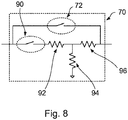
- the attenuator 70 includes resistors 92, 94, 96.
- the resistors 92, 96 are fixed (non-variable) resistors.
- the resistors 92, 96 are arranged in series in the receive path 34.
- the resistor 94 is connected between ground and a node located in-between the two series connected resistors 92, 96.
- a further switch 90 is provided in series with the two series connected resistors 92, 96.
- This switch 90 may operate similarly to the switch 72, as described above.
- the switches 72, 90 may operate together for decoupling the receive path 34 from the first differential output 4 when the transmit path 36 is active.
- the attenuation provided by the attenuator 70 may be varied by opening/closing the switches 72, 90.
- each resistor 74, 76, 78, 75, 77, 79 may be variable resistors.
- each resistor 74, 76, 78, 75, 77, 79 may comprise a programmable bank of resistors.
- An example of such a resistor bank 80 is shown in Figure 6 .
- the resistor bank 80 in Figure 6 includes a plurality of resistors 84 arranged in parallel. Each resistor 84 may be connected in series with a respective switch 82. By selectively opening and closing one or more of the switches 82, the resistor provided by the resistor bank 80 may be varied.
- the switches 82 may be programmable. As noted previously, it is further envisaged that the switches 82 may themselves also operate to may operate as described above for decoupling the receive path 34 from the first differential output 4 when the transmit path 36 is active.
- the attenuators described herein may be fixed or may programmable by software or by an Automatic Gain Control (AGC) algorithm.
- AGC Automatic Gain Control
- an integrated circuit comprising a transceiver including a transformer.
- the transformer includes an input coupled to one or more primary windings.
- the transformer also includes a first differential output coupled to a first set of one or more secondary windings.
- the transformer further includes a second differential output coupled to a second, different set of one or more secondary windings.
- a method of making an integrated circuit comprising a transceiver. The method includes forming a plurality of components on and/or in a semiconductor substrate. At least one of the components comprises a transformer.
- the method includes forming the transformer by forming one or more primary windings coupled to an input, forming a first set of one or more secondary windings coupled to a first differential output, and forming a second, different set of one or more secondary windings coupled to a second differential output.
Landscapes
- Engineering & Computer Science (AREA)
- Power Engineering (AREA)
- Multimedia (AREA)
- Computer Networks & Wireless Communication (AREA)
- Signal Processing (AREA)
- Manufacturing & Machinery (AREA)
- Microelectronics & Electronic Packaging (AREA)
- Semiconductor Integrated Circuits (AREA)
- Dc Digital Transmission (AREA)
Abstract
Description
- The present specification relates to an integrated circuit comprising a transceiver, the transceiver including a transformer. The present specification also relates to a method of making an integrated circuit comprising a transceiver.
- In modern integrated transceivers, the Radio Frequency (RF) signal is typically a differential signal. An external balun is often used to perform the single ended to differential conversion between an antenna and an integrated transceiver having a differential input. The use of an integrated transformer may avoid the use of an external balun, and may lead to cost reductions.
- Aspects of the present disclosure are set out in the accompanying independent and dependent claims. Combinations of features from the dependent claims may be combined with features of the independent claims as appropriate and not merely as explicitly set out in the claims.
- According to an aspect of the present disclosure, there is provided an integrated circuit comprising a transceiver, the transceiver including a transformer, the transformer comprising:
- an input coupled to one or more primary windings of the transformer;
- a first differential output coupled to a first set of one or more secondary windings of the transformer;
- a second differential output coupled to a second, different set of one or more secondary windings of the transformer.
- According to another aspect of the present disclosure, there is provided a method of making an integrated circuit comprising a transceiver, the method comprising:
- providing a semiconductor substrate; and
- forming a plurality of components on and/or in the semiconductor substrate, wherein at least one of the components comprises a transformer, and wherein the method includes forming the transformer by:
- forming one or more primary windings coupled to an input of the transformer;
- forming a first set of one or more secondary windings coupled to a first differential output of the transformer; and
- forming a second, different set of one or more secondary windings coupled to a second differential output of the transformer.
- The provision of a transceiver including a transformer integrated in an integrated circuit can reduce the cost and size of the transceiver. Moreover, since the transformer has separate outputs, each with its own set of associated windings, these outputs can be independently tailored to different applications.
- For instance, in one embodiment, the first differential output may be coupled to a receive path of the transceiver while the second differential output may be coupled to a transmit path of the transceiver. The secondary windings and corresponding outputs can be separately tailored for use with their respective receive/transmit paths.
- In some embodiments, the receive path may include a switch that is switchable between an ON state for coupling the receive path to the first differential output and an OFF state for decoupling the receive path from the first differential output. The switch may be operable switch to the OFF state to decouple the receive path from the first differential output when the transmit path is active. This may avoid high voltage swings coming into the receive path, which may prevent damage of potentially sensitive components of the receive path.
- The switch may be included in an attenuator of the receive path. In some examples, more than one switch having the functionality set out above may be included in the attenuator. Each switch may thus be switchable between an ON state for coupling the receive path to the first differential output when the transmit path is not active and an OFF state for decoupling the receive path from the first differential output when the transmit path is active. In some examples, where more than one such switch is included in the attenuator, the switches may operate together (e.g. be operable to switch together (e.g. substantially at the same time)) to couple/decouple the receive path and the first differential output.
- The integrated circuit may include a centre tap. The centre tap may be coupled to the first set of secondary winding(s). This may allow the operation of the switch to be optimised. For instance, the center tap may be operable to connect to ground when the switch is in the ON state. This may reduce the ON state resistance of the switch. The center tap may be operable to connect to a supply voltage of the integrated circuit or to a voltage intermediate the supply voltage and ground when the switch is in the OFF state. This may reduce to OFF state capacitance of the switch.
- The input may be coupled to an antenna.
- The first set of secondary winding(s) may have a different number of windings to the second set of secondary winding(s). In this way, the first set of secondary winding(s) may have a different winding ratio with respect to the primary winding(s) than the second set of secondary winding(s). This can allow the transformer to be tuned/optimised for particular applications (e.g. the specific configuration of the receive path and/or the transmit path).
- The integrated circuit may further include a capacitor bank coupled to at least some of the windings of the transformer for tuning an operating frequency of the transformer.
- The primary and secondary winding(s) of the transformer may be substantially concentric. The primary and secondary winding(s) of the transformer may be formed from electrically conductive tracks arranged on a surface of a semiconductor substrate of the integrated circuit, allowing them to be conveniently produced (e.g. as part of BEOL processing). The primary winding(s) and at least one of the sets of secondary winding(s) may be arranged in a common plane. The primary winding(s) may be arranged in-between some of the secondary winding(s) in the common plane, when viewed from above the surface of the semiconductor substrate. The windings of at least one of the sets of secondary winding(s) may be arranged in more than one plane.
- These arrangements of the winding(s) of the transformer may allow the transformer conveniently and compactly to be integrated on a semiconductor die.
- The input may be a differential input.
- Embodiments of this disclosure will be described hereinafter, by way of example only, with reference to the accompanying drawings in which like reference signs relate to like elements and in which:
-
Figures 1A, 1B and 1C show the primary and secondary windings of a transformer in accordance with an embodiment of the present disclosure; -
Figure 2 shows a cross-section of part of the transformer ofFigure 1 ; -
Figure 3 shows a transceiver in accordance with an embodiment of the present disclosure; -
Figure 4 shows a capacitor bank in accordance with an embodiment of the present disclosure; -
Figure 5A shows a switch in series with an attenuator in accordance with an embodiment of the present disclosure; -
Figure 5B shows an attenuator in accordance with an embodiment of the present disclosure; -
Figure 6 shows a resistor bank in accordance with an embodiment of the present disclosure; -
Figure 7 shows an attenuator in accordance with an embodiment of the present disclosure; and -
Figure 8 shows an attenuator in accordance with an embodiment of the present disclosure. - Embodiments of this disclosure are described in the following with reference to the accompanying drawings.
-
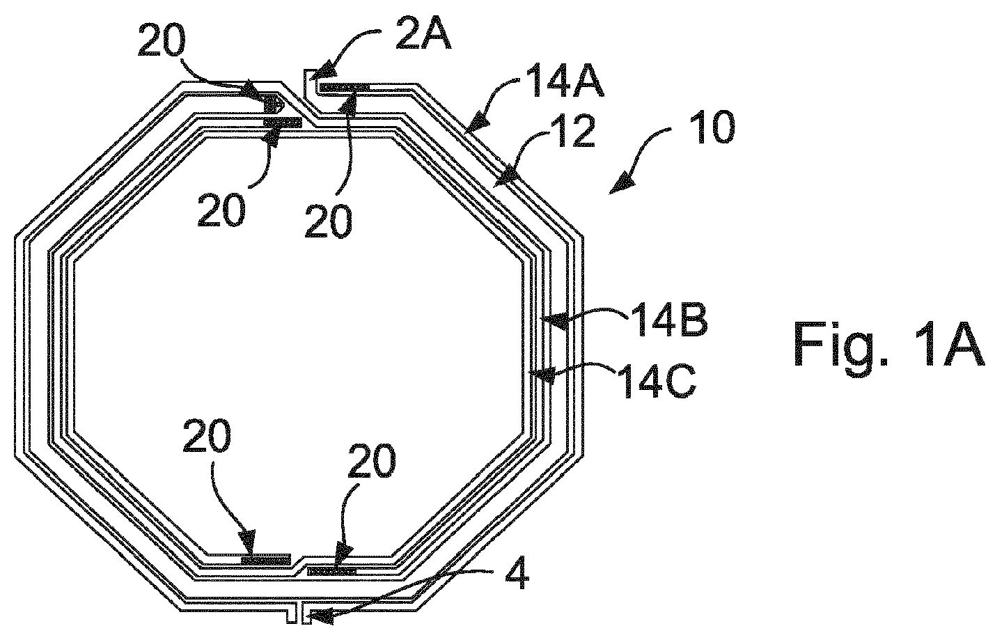
Figures 1A, 1B and 1C show the primary and secondary windings of atransformer 10 in accordance with an embodiment of the present disclosure.Figure 2 shows a cross-section of part of thetransformer 10 ofFigure 1 . - The
transformer 10 may include in an integrated transceiver, provided on or in a semiconductor substrate. Further example features of such a transceiver will be discussed in more detail below. The windings of thetransformer 10 may be formed on or above a major surface of the semiconductor substrate in which the transceiver is integrated. For instance, the windings of thetransformer 10 may be formed from the patterned metal layers (e.g. metal tracks) of ametallisation stack 20. Accordingly, the transformer may be manufactured using standard Back End of Line (BEOL) processing techniques. The laminated configuration of the windings in this embodiment can be most clearly appreciated fromFigure 2 . As is known in the art, the conductive features in thestack 26 may be separated by intervening dielectric layers. One or more capping layers (scratch protection layers) may be located at or near the top of thestack 26. - The transformer includes one or more
primary windings 12. The transformer also includes a first set of one or moresecondary windings 14. The transformer further includes a second set of one or moresecondary windings 16. The primary and secondary windings of thetransformer 10 in the present example are substantially hexagonal, although other shapes are envisaged. The primary 12 and secondary winding(s) 14, 16 of thetransformer 10 may be substantially concentric. - In the present example, the windings of the
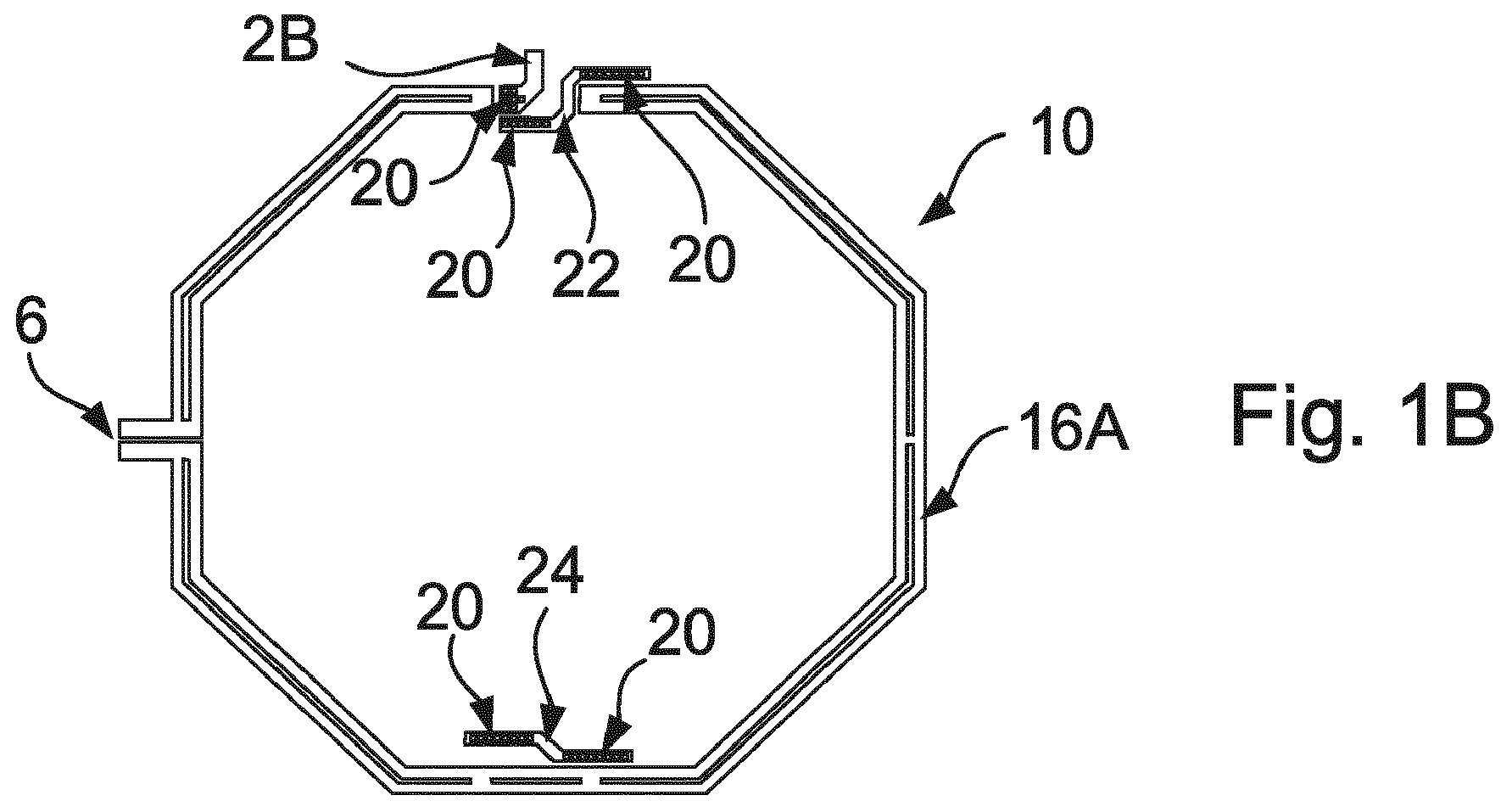
transformer 10 are laminated (e.g. provided in the various layers of a metallisation stack. A first layer (e.g. uppermost layer) may include the features shown inFigure 1A . A second layer (e.g. intermediate layer) may include the features shown in Figure IB. A third layer (e.g. lowermost layer) may include the features shown inFigure 1C . - In the present example, the one or more
primary windings 12 of thetransformer 10 are located in the first layer (Figure 1A ). The first layer also includes a first set of one or moresecondary windings 14 of the transformer. Thesecondary windings 14 in this example include an outermost secondary winding 14A and one or more innersecondary windings secondary windings 14. For example, as shown inFigure 1A , the primary winding(s) 12 may be located in-between the outermost secondary winding 14A and the one or more innersecondary windings - In the present example, the second set of one or more
secondary windings 16 is located in the second layer (see the secondary windings labelled 16A) and the third layer (see the secondary windings labelled 16A). - The
transformer 10 may also include features for interconnecting the various windings. For instance, metal filledvias 20 may extend between the layers to form interconnections of this kind. In another example, the second layer shown inFigure 1B includes abridge portion 22, which is used to cross the winding 14 over the one or moreprimary windings 12 in the first layer. Similarly, thebridge portion 24 located in the second layer (Figure 1B ) is used to cross the winding 14 over itself in the first layer. As can be seen inFigure 2 , metal filledvias 20 may also interconnect the features of the second set of one or moresecondary windings 16 located in the second and third layers. - The transformer also includes an input 2 and two
outputs 4, 6. Theoutputs 4, 6 are both differential outputs. In this example, input 2 is a differential input. - The input 2 is coupled to the one or more
primary windings 12 of thetransformer 10. The input 2 in this example includes afirst terminal 2A located in the first layer (Figure 1A ) and asecond terminal 2B located in the second layer (Figure 1B ). Note that thesecond terminal 2B is coupled to one end of the one or moreprimary windings 12 in the first layer by metal filledvias 20. - The output 4 is coupled to the ends of the first set of one or more
secondary windings 14 of thetransformer 10. Theoutput 6 is coupled to the ends of the second set of one or moresecondary windings 16 of thetransformer 10. - The first set of secondary winding(s) 14 may have a different number of windings to the second set of secondary winding(s) 16. In this way, the first set of secondary winding(s) 14 may have a different winding ratio with respect to the primary winding(s) 12 than the second set of secondary winding(s) 16. This can allow the
transformer 10 to be tuned/optimised for particular applications (e.g. the specific configuration of the receive path and/or the transmit path to be described in more detail below). -
Figure 3 shows atransceiver 30 in accordance with an embodiment of the present disclosure. As noted previously, the components of thetransceiver 30 may be integrated in a semiconductor substrate. Thetransceiver 30 includes atransformer 10 of the kind described above.Figure 3 schematically shows the primary 12 and first andsecond sets transformer 10. - The
transceiver 30 in this example includes a receivepath 34 and a transmitpath 36. The first differential output 4 of thetransformer 10 is coupled to the receivepath 34. The seconddifferential output 6 of thetransformer 10 is coupled to the transmitpath 36. The input 2 may be coupled to anantenna 38. In the present example, afirst terminal 2A/2B of the input 2 is coupled to an antenna, while theother terminal 2B/2A is coupled toground 42. - The
transceiver 30 in this example includes a number ofcapacitor banks 32. Thesecapacitor banks 32 may be coupled to thewindings transformer 10 for tuning an operating frequency of the transformer.Figure 4 shows an example of such acapacitor bank 32. Thecapacitor bank 32 includes a plurality ofcapacitors 60 arranged in parallel. Eachcapacitor 60 may be connected in series with arespective switch 62. By selectively opening and closing one or more of theswitches 62, the capacitance added to the circuit by the capacitor back 32 may be varied. Theswitches 62 may be programmable. In some examples, the switches may be operable to open/close to compensate for manufacturing variations and/or environmental factors (e.g. temperature). - In some embodiments, the receive
path 34 may include aswitch 40. The switch may be switchable between an ON state and an OFF state. Theswitch 40 may be implemented using one or more MOS transistors (e.g. NMOS). - In the ON state, the
switch 40 couples the receivepath 34 to the first differential output 4 of thetransformer 10. In the OFF state, theswitch 40 decouples the receivepath 34 from the first differential output 4. Theswitch 40 may be operable switch to the OFF state to decouple the receivepath 34 from the first differential output 4 when the transmitpath 36 is active. This may avoid high voltage swings coming into the receivepath 34 from the transmitpath 36, which may prevent damage of potentially sensitive components of the receivepath 34. - In some embodiments, the
transformer 10 may include a number of centre taps. In the example shown inFigure 3 , thetransformer 10 is provided with afirst centre tap 44 and asecond centre tap 46. Thefirst centre tap 44 is coupled to the first set of secondary winding(s) 14. Thesecond centre tap 46 is coupled to the second set of secondary winding(s) 16. The centre taps may allow the common mode voltage of the receivepath 34 and the transmitpath 36 to be fixed. - Voltages may be applied (e.g. programmably) to the
centre tap 44 for optimising the performance of theswitch 40. For instance, thecenter tap 44 may be operable to couple to ground when the switch is in the ON state. This may reduce the ON state resistance of a MOS transistor forming theswitch 40. Also, when the input level is high (e.g. (10dBm)) this may reduce or prevent clipping of the signal by a parasitic diode formed by the drain-bulk junction of the switch. Thecenter tap 44 may also be operable to couple to a supply voltage of the integrated circuit or to a voltage intermediate the supply voltage and ground when the switch is in the OFF state. This may reduce to OFF state capacitance of a MOS transistor forming the switch. Also, when the output level is high (e.g. (10dBm)) this may similarly reduce or prevent clipping of the signal. - The receive
path 34 and transmitpath 36 of thetransceiver 30 may include a number components for processing a signal to be sent/received by theantenna 38 via thetransformer 10. For instance, the receivepath 34 may include one or more of: an amplifier (e.g. a low noise amplifier (LNA) 44), amixer 46, an intermediate frequency (IF) filter and an analogue todigital converter 50. The transmitpath 36 may include one or more of: apower amplifier 52, a phase locked loop (PLL) 54 and a digital toanalogue converter 56. - The receive
path 34 may also include an attenuator (not shown inFigure 3 ). The attenuator may, for instance, be located between theswitch 40 and thelow noise amplifier 44. -
Figure 5A shows a part of the receivepath 34 including theswitch 40 and anattenuator 70. Theattenuator 70 includesresistors resistors path 34. Theresistor 78 is connected between ground and a node located in-between the two series connectedresistors attenuator 70 includes aswitch 72 arranged in parallel with the series connected pair ofresistors switch 72 may be closed so as to bypass the resistors of theattenuator 70, or opened so that theattenuator 70 attenuates the signal in the receivepath 34. During operation, the attenuation provided by theattenuator 70 may be varied by varying theresistors switch 72. - It is envisaged that the function of the
switch 40 may incorporated into theattenuator 70. This may allow theswitch 40 to be omitted. An example of this is shown inFigure 5B . - The
attenuator 70 shown inFigure 5B has a similar construction to that of theattenuator 70 inFigure 5A . However, theswitch 72 in theattenuator 70 inFigure 5B is operable to function in a manner similar to that described above in respect of theswitch 40. E.g. theswitch 72 may be operable switch to an OFF state to decouple the receivepath 34 from the first differential output 4 when the transmitpath 36 is active. As described previously, this may avoid high voltage swings coming into the receivepath 34 from the transmitpath 36. In this embodiment, at least some of theresistors Figure 6 , in which theswitches 82 of the resistor bank(s) may also operate (i.e. be opened) to decouple the receivepath 34 from the first differential output 4 when the transmitpath 36 is active. In this way, high voltage swings through theresistors path 34 from the transmitpath 36 may be avoid when theswitch 72 is in the OFF state. -
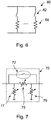
Figure 7 shows another example of anattenuator 70, which may be included in the receivepath 34. In this example, theattenuator 70 includes aswitch 72, which operates in a manner similar to that described above in respect ofFigure 5B . InFigure 7 , theattenuator 70 includesresistors resistor 75 is arranged in series in the receivepath 34. Theresistor 77 is connected between ground and an end of theresistor 75 closest thetransformer 10. Theresistor 79 is connected between ground and an end of theresistor 75 furthest from thetransformer 10. During operation, the attenuation provided by theattenuator 70 may be varied by varying theresistors switch 72. As with the example ofFigure 5B , at least some of theresistors Figure 6 , in which theswitches 82 of the resistor bank(s) may also operate (i.e. be opened) to decouple the receivepath 34 from the first differential output 4 when the transmitpath 36 is active. In this way, high voltage swings through theresistors path 34 from the transmitpath 36 may be avoided when theswitch 72 is in the OFF state. -
Figure 8 shows a further example of anattenuator 70, which may be included in the receivepath 34. In this example, theattenuator 70 includes aswitch 72, which operates in a manner similar to that described above in respect ofFigure 5B . InFigure 8 , theattenuator 70 includesresistors resistors resistors path 34. Theresistor 94 is connected between ground and a node located in-between the two series connectedresistors further switch 90 is provided in series with the two series connectedresistors switch 90 may operate similarly to theswitch 72, as described above. In particular, in this embodiment, it is envisaged that theswitches path 34 from the first differential output 4 when the transmitpath 36 is active. During operation, the attenuation provided by theattenuator 70 may be varied by opening/closing theswitches - In each example attenuator in which variable resistors are used, it is envisaged that the
resistors resistor resistor bank 80 is shown inFigure 6 . Theresistor bank 80 inFigure 6 includes a plurality ofresistors 84 arranged in parallel. Eachresistor 84 may be connected in series with arespective switch 82. By selectively opening and closing one or more of theswitches 82, the resistor provided by theresistor bank 80 may be varied. Theswitches 82 may be programmable. As noted previously, it is further envisaged that theswitches 82 may themselves also operate to may operate as described above for decoupling the receivepath 34 from the first differential output 4 when the transmitpath 36 is active. - It is envisaged that the resistors of the
example attenuators 70 described herein may be replaced with capacitors. As with the resistors described above, it is envisaged that the capacitors may be variable capacitors and/or may be implemented using a capacitor bank. The capacitor bank(s) may be similar to theresistor bank 80 shown inFigure 6 , in which theresistors 84 are replaced with capacitors. - The attenuators described herein may be fixed or may programmable by software or by an Automatic Gain Control (AGC) algorithm.
- Accordingly, there has been described an integrated circuit comprising a transceiver including a transformer. The transformer includes an input coupled to one or more primary windings. The transformer also includes a first differential output coupled to a first set of one or more secondary windings. The transformer further includes a second differential output coupled to a second, different set of one or more secondary windings. A method of making an integrated circuit comprising a transceiver. The method includes forming a plurality of components on and/or in a semiconductor substrate. At least one of the components comprises a transformer. The method includes forming the transformer by forming one or more primary windings coupled to an input, forming a first set of one or more secondary windings coupled to a first differential output, and forming a second, different set of one or more secondary windings coupled to a second differential output.
- Although particular embodiments of this disclosure have been described, it will be appreciated that many modifications/additions and/or substitutions may be made within the scope of the claims.
Claims (15)
- An integrated circuit comprising a transceiver, the transceiver including a transformer, the transformer comprising:an input coupled to one or more primary windings of the transformer;a first differential output coupled to a first set of one or more secondary windings of the transformer;a second differential output coupled to a second, different set of one or more secondary windings of the transformer.
- The integrated circuit of claim 1, wherein:the first differential output is coupled to a receive path of the transceiver; andthe second differential output is coupled to a transmit path of the transceiver.
- The integrated circuit of claim 2, wherein the receive path includes a switch that is switchable between:an ON state for coupling the receive path to the first differential output; andan OFF state for decoupling the receive path from the first differential output, wherein the switch is operable switch to said OFF state to decouple the receive path from the first differential output when the transmit path is active.
- The integrated circuit of claim 3, wherein the switch is included in an attenuator of the receive path.
- The integrated circuit of claim 3 or claim 4, comprising a centre tap coupled to the first set of secondary winding(s), wherein the center tap is operable to:connect to ground when the switch is in the ON state; andconnect to a supply voltage of the integrated circuit or to a voltage intermediate the supply voltage and ground when the switch is in the OFF state.
- The integrated circuit of any preceding claim, wherein the input is coupled to an antenna.
- The integrated circuit of any preceding claim, wherein the first set of secondary winding(s) has a different number of windings to the second set of secondary winding(s), whereby the first set of secondary winding(s) has a different winding ratio with respect to the primary winding(s) than the second set of secondary winding(s).
- The integrated circuit of any preceding claim, further comprising a capacitor bank coupled to at least some of the windings of the transformer for tuning an operating frequency of the transformer.
- The integrated circuit of any preceding claim, wherein the primary and secondary winding(s) of the transformer are substantially concentric.
- The integrated circuit of any preceding claim, wherein the primary and secondary winding(s) of the transformer comprise electrically conductive tracks arranged on a surface of a semiconductor substrate of the integrated circuit.
- The integrated circuit of claim 10, wherein the primary winding(s) and at least one of said sets of secondary winding(s) are arranged in a common plane.
- The integrated circuit of claim 11, wherein the primary winding(s) are arranged in-between some of the secondary winding(s) in said common plane, when viewed from above the surface of the semiconductor substrate.
- The integrated circuit of any preceding claim, wherein the windings of at least one of said sets of secondary winding(s) are arranged in more than one plane.
- The integrated circuit of any preceding claim, wherein the input is a differential input.
- A method of making an integrated circuit comprising a transceiver, the method comprising:providing a semiconductor substrate; andforming a plurality of components on and/or in the semiconductor substrate, wherein at least one of said components comprises a transformer, and wherein the method includes forming the transformer by:forming one or more primary windings coupled to an input of the transformer;forming a first set of one or more secondary windings coupled to a first differential output of the transformer; andforming a second, different set of one or more secondary windings coupled to a second differential output of the transformer.
Priority Applications (3)
| Application Number | Priority Date | Filing Date | Title |
|---|---|---|---|
| EP17306368.6A EP3471140B1 (en) | 2017-10-11 | 2017-10-11 | Integrated circuit including a plurality of components including a transformer |
| US16/046,191 US10367539B2 (en) | 2017-10-11 | 2018-07-26 | Integrated circuit including a plurality of components including a transformer |
| CN201811187058.6A CN109659120B (en) | 2017-10-11 | 2018-10-11 | Integrated circuit containing multiple components including a transformer |
Applications Claiming Priority (1)
| Application Number | Priority Date | Filing Date | Title |
|---|---|---|---|
| EP17306368.6A EP3471140B1 (en) | 2017-10-11 | 2017-10-11 | Integrated circuit including a plurality of components including a transformer |
Publications (2)
| Publication Number | Publication Date |
|---|---|
| EP3471140A1 true EP3471140A1 (en) | 2019-04-17 |
| EP3471140B1 EP3471140B1 (en) | 2022-05-18 |
Family
ID=60162156
Family Applications (1)
| Application Number | Title | Priority Date | Filing Date |
|---|---|---|---|
| EP17306368.6A Active EP3471140B1 (en) | 2017-10-11 | 2017-10-11 | Integrated circuit including a plurality of components including a transformer |
Country Status (3)
| Country | Link |
|---|---|
| US (1) | US10367539B2 (en) |
| EP (1) | EP3471140B1 (en) |
| CN (1) | CN109659120B (en) |
Cited By (1)
| Publication number | Priority date | Publication date | Assignee | Title |
|---|---|---|---|---|
| CN115053455A (en) * | 2019-12-10 | 2022-09-13 | 瑞典爱立信有限公司 | Compact antenna impedance tuner |
Families Citing this family (4)
| Publication number | Priority date | Publication date | Assignee | Title |
|---|---|---|---|---|
| KR102678310B1 (en) * | 2019-06-11 | 2024-06-25 | 삼성전자주식회사 | Switching transformer and electronic device including thereof |
| US11380988B2 (en) | 2020-11-13 | 2022-07-05 | Qualcomm Incorporated | Antenna switching scheme |
| US12340928B2 (en) | 2020-11-18 | 2025-06-24 | Realtek Semiconductor Corporation | Transformer device |
| TWI748878B (en) * | 2020-11-18 | 2021-12-01 | 瑞昱半導體股份有限公司 | Transformer device |
Citations (5)
| Publication number | Priority date | Publication date | Assignee | Title |
|---|---|---|---|---|
| US20060270377A1 (en) * | 2005-05-25 | 2006-11-30 | Broadcom Corporation | Transformer-based multi-band RF front-end architecture |
| US20090284339A1 (en) * | 2008-05-14 | 2009-11-19 | Samsung Electronics Co., Ltd. | Transformers, balanced-unbalanced transformers (baluns) and Integrated circuits including the same |
| US20120025927A1 (en) * | 2010-07-28 | 2012-02-02 | Qualcomm Incorporated | Rf isolation switch circuit |
| US20130157587A1 (en) * | 2011-12-20 | 2013-06-20 | Stmicroelectronics S.A. | Integrated circuit comprising an integrated transformer of the "balun" type with several input and output channels |
| WO2017099578A1 (en) * | 2015-12-07 | 2017-06-15 | Greenpeak Technologies B.V. | On-chip balun circuit and multi-port antenna switch circuit |
Family Cites Families (12)
| Publication number | Priority date | Publication date | Assignee | Title |
|---|---|---|---|---|
| EP1564897A1 (en) * | 2004-02-13 | 2005-08-17 | Thomson Licensing S.A. | Control of a power amplifier for reducing power consumption in a transceiver |
| US7269391B2 (en) * | 2004-03-16 | 2007-09-11 | Broadcom Corporation | Tunable transceiver front end |
| US7848713B2 (en) * | 2007-09-10 | 2010-12-07 | Qualcomm Incorporated | Common mode signal attenuation for a differential duplexer |
| US8229367B2 (en) | 2009-04-14 | 2012-07-24 | Qualcomm, Incorporated | Low noise amplifier with combined input matching, balun, and transmit/receive switch |
| US8493126B2 (en) * | 2010-07-15 | 2013-07-23 | Qualcomm Incorporated | Wideband balun having a single primary and multiple secondaries |
| US8666330B2 (en) * | 2010-09-30 | 2014-03-04 | St-Ericsson Sa | Antenna switch with ESD isolation |
| US9083293B2 (en) * | 2011-05-19 | 2015-07-14 | Mediatek Inc. | Signal transceiver |
| TWI445330B (en) * | 2012-04-06 | 2014-07-11 | Realtek Semiconductor Corp | Transceiver having an on-chip co-transformer |
| CN103684518A (en) * | 2012-09-18 | 2014-03-26 | 北京中电华大电子设计有限责任公司 | Radio frequency circuit shared by transmitting and receiving matching networks based on on-chip transformer |
| US9431473B2 (en) | 2012-11-21 | 2016-08-30 | Qualcomm Incorporated | Hybrid transformer structure on semiconductor devices |
| US20140361814A1 (en) * | 2013-06-11 | 2014-12-11 | Futurewei Technologies, Inc. | High Speed Latch |
| EP3182169B1 (en) * | 2015-12-17 | 2018-12-05 | Mettler-Toledo Safeline Limited | Metal detection apparatus |
-
2017
- 2017-10-11 EP EP17306368.6A patent/EP3471140B1/en active Active
-
2018
- 2018-07-26 US US16/046,191 patent/US10367539B2/en active Active
- 2018-10-11 CN CN201811187058.6A patent/CN109659120B/en active Active
Patent Citations (5)
| Publication number | Priority date | Publication date | Assignee | Title |
|---|---|---|---|---|
| US20060270377A1 (en) * | 2005-05-25 | 2006-11-30 | Broadcom Corporation | Transformer-based multi-band RF front-end architecture |
| US20090284339A1 (en) * | 2008-05-14 | 2009-11-19 | Samsung Electronics Co., Ltd. | Transformers, balanced-unbalanced transformers (baluns) and Integrated circuits including the same |
| US20120025927A1 (en) * | 2010-07-28 | 2012-02-02 | Qualcomm Incorporated | Rf isolation switch circuit |
| US20130157587A1 (en) * | 2011-12-20 | 2013-06-20 | Stmicroelectronics S.A. | Integrated circuit comprising an integrated transformer of the "balun" type with several input and output channels |
| WO2017099578A1 (en) * | 2015-12-07 | 2017-06-15 | Greenpeak Technologies B.V. | On-chip balun circuit and multi-port antenna switch circuit |
Cited By (2)
| Publication number | Priority date | Publication date | Assignee | Title |
|---|---|---|---|---|
| CN115053455A (en) * | 2019-12-10 | 2022-09-13 | 瑞典爱立信有限公司 | Compact antenna impedance tuner |
| CN115053455B (en) * | 2019-12-10 | 2025-10-03 | 瑞典爱立信有限公司 | Compact Antenna Impedance Tuner |
Also Published As
| Publication number | Publication date |
|---|---|
| EP3471140B1 (en) | 2022-05-18 |
| US20190109612A1 (en) | 2019-04-11 |
| US10367539B2 (en) | 2019-07-30 |
| CN109659120B (en) | 2024-07-16 |
| CN109659120A (en) | 2019-04-19 |
Similar Documents
| Publication | Publication Date | Title |
|---|---|---|
| US10367539B2 (en) | Integrated circuit including a plurality of components including a transformer | |
| US9166640B2 (en) | Adjustable impedance matching network | |
| US10193521B2 (en) | Adjustable impedance matching network | |
| CN108292911B (en) | Low phase shift high frequency attenuator | |
| US7526256B2 (en) | Transformer-based multi-band RF front-end architecture | |
| KR101234957B1 (en) | Apparatus for controlling power with an output network | |
| US9300286B2 (en) | Antenna transmit receive switch | |
| CN108476031A (en) | Adaptive Tuning Networks for Composable Filters | |
| WO2014193501A1 (en) | Signal handling apparatus for improving linearity of radio frequency circuits | |
| KR20170093208A (en) | Adjustable rf coupler | |
| CN1954489A (en) | Multi-band low noise amplifier system | |
| US10079586B2 (en) | Package for a tunable filter | |
| US20140139298A1 (en) | Rf switch with transformer and switching method thereof | |
| US20070115086A1 (en) | Multilayer circuit with variable inductor, and method of manufacturing it | |
| CN116208109A (en) | Phase shifter with controllable attenuation and control method thereof | |
| US9667217B2 (en) | High performance integrated tunable impedance matching network with coupled merged inductors | |
| EP3742611A1 (en) | Impedance matching circuit, radio frequency circuit and method | |
| Ji et al. | A multiband directional coupler using SOI CMOS for RF front-end applications | |
| JP4471757B2 (en) | Variable inductor | |
| US20230022015A1 (en) | Compact Antenna Impedance Tuner | |
| Qureshi et al. | A low-loss compact linear varactor based phase-shifter | |
| US12244288B2 (en) | Balun with improved common mode rejection ratio | |
| US20240146289A1 (en) | Tuning device, system and method |
Legal Events
| Date | Code | Title | Description |
|---|---|---|---|
| PUAI | Public reference made under article 153(3) epc to a published international application that has entered the european phase |
Free format text: ORIGINAL CODE: 0009012 |
|
| STAA | Information on the status of an ep patent application or granted ep patent |
Free format text: STATUS: THE APPLICATION HAS BEEN PUBLISHED |
|
| AK | Designated contracting states |
Kind code of ref document: A1 Designated state(s): AL AT BE BG CH CY CZ DE DK EE ES FI FR GB GR HR HU IE IS IT LI LT LU LV MC MK MT NL NO PL PT RO RS SE SI SK SM TR |
|
| AX | Request for extension of the european patent |
Extension state: BA ME |
|
| STAA | Information on the status of an ep patent application or granted ep patent |
Free format text: STATUS: REQUEST FOR EXAMINATION WAS MADE |
|
| 17P | Request for examination filed |
Effective date: 20191017 |
|
| RBV | Designated contracting states (corrected) |
Designated state(s): AL AT BE BG CH CY CZ DE DK EE ES FI FR GB GR HR HU IE IS IT LI LT LU LV MC MK MT NL NO PL PT RO RS SE SI SK SM TR |
|
| STAA | Information on the status of an ep patent application or granted ep patent |
Free format text: STATUS: EXAMINATION IS IN PROGRESS |
|
| 17Q | First examination report despatched |
Effective date: 20210219 |
|
| GRAP | Despatch of communication of intention to grant a patent |
Free format text: ORIGINAL CODE: EPIDOSNIGR1 |
|
| STAA | Information on the status of an ep patent application or granted ep patent |
Free format text: STATUS: GRANT OF PATENT IS INTENDED |
|
| RIC1 | Information provided on ipc code assigned before grant |
Ipc: H03H 7/25 20060101ALI20220118BHEP Ipc: H01L 49/02 20060101ALI20220118BHEP Ipc: H01L 23/66 20060101ALI20220118BHEP Ipc: H01F 27/28 20060101ALI20220118BHEP Ipc: H01F 17/00 20060101ALI20220118BHEP Ipc: H01L 23/64 20060101ALI20220118BHEP Ipc: H01F 19/04 20060101ALI20220118BHEP Ipc: H01P 5/10 20060101ALI20220118BHEP Ipc: H03H 7/42 20060101ALI20220118BHEP Ipc: H01L 23/522 20060101AFI20220118BHEP |
|
| INTG | Intention to grant announced |
Effective date: 20220217 |
|
| GRAS | Grant fee paid |
Free format text: ORIGINAL CODE: EPIDOSNIGR3 |
|
| GRAA | (expected) grant |
Free format text: ORIGINAL CODE: 0009210 |
|
| STAA | Information on the status of an ep patent application or granted ep patent |
Free format text: STATUS: THE PATENT HAS BEEN GRANTED |
|
| AK | Designated contracting states |
Kind code of ref document: B1 Designated state(s): AL AT BE BG CH CY CZ DE DK EE ES FI FR GB GR HR HU IE IS IT LI LT LU LV MC MK MT NL NO PL PT RO RS SE SI SK SM TR |
|
| REG | Reference to a national code |
Ref country code: GB Ref legal event code: FG4D |
|
| REG | Reference to a national code |
Ref country code: CH Ref legal event code: EP |
|
| REG | Reference to a national code |
Ref country code: IE Ref legal event code: FG4D |
|
| REG | Reference to a national code |
Ref country code: DE Ref legal event code: R096 Ref document number: 602017057576 Country of ref document: DE |
|
| REG | Reference to a national code |
Ref country code: AT Ref legal event code: REF Ref document number: 1493635 Country of ref document: AT Kind code of ref document: T Effective date: 20220615 |
|
| REG | Reference to a national code |
Ref country code: LT Ref legal event code: MG9D |
|
| REG | Reference to a national code |
Ref country code: NL Ref legal event code: MP Effective date: 20220518 |
|
| REG | Reference to a national code |
Ref country code: AT Ref legal event code: MK05 Ref document number: 1493635 Country of ref document: AT Kind code of ref document: T Effective date: 20220518 |
|
| PG25 | Lapsed in a contracting state [announced via postgrant information from national office to epo] |
Ref country code: SE Free format text: LAPSE BECAUSE OF FAILURE TO SUBMIT A TRANSLATION OF THE DESCRIPTION OR TO PAY THE FEE WITHIN THE PRESCRIBED TIME-LIMIT Effective date: 20220518 Ref country code: PT Free format text: LAPSE BECAUSE OF FAILURE TO SUBMIT A TRANSLATION OF THE DESCRIPTION OR TO PAY THE FEE WITHIN THE PRESCRIBED TIME-LIMIT Effective date: 20220919 Ref country code: NO Free format text: LAPSE BECAUSE OF FAILURE TO SUBMIT A TRANSLATION OF THE DESCRIPTION OR TO PAY THE FEE WITHIN THE PRESCRIBED TIME-LIMIT Effective date: 20220818 Ref country code: NL Free format text: LAPSE BECAUSE OF FAILURE TO SUBMIT A TRANSLATION OF THE DESCRIPTION OR TO PAY THE FEE WITHIN THE PRESCRIBED TIME-LIMIT Effective date: 20220518 Ref country code: LT Free format text: LAPSE BECAUSE OF FAILURE TO SUBMIT A TRANSLATION OF THE DESCRIPTION OR TO PAY THE FEE WITHIN THE PRESCRIBED TIME-LIMIT Effective date: 20220518 Ref country code: HR Free format text: LAPSE BECAUSE OF FAILURE TO SUBMIT A TRANSLATION OF THE DESCRIPTION OR TO PAY THE FEE WITHIN THE PRESCRIBED TIME-LIMIT Effective date: 20220518 Ref country code: GR Free format text: LAPSE BECAUSE OF FAILURE TO SUBMIT A TRANSLATION OF THE DESCRIPTION OR TO PAY THE FEE WITHIN THE PRESCRIBED TIME-LIMIT Effective date: 20220819 Ref country code: FI Free format text: LAPSE BECAUSE OF FAILURE TO SUBMIT A TRANSLATION OF THE DESCRIPTION OR TO PAY THE FEE WITHIN THE PRESCRIBED TIME-LIMIT Effective date: 20220518 Ref country code: ES Free format text: LAPSE BECAUSE OF FAILURE TO SUBMIT A TRANSLATION OF THE DESCRIPTION OR TO PAY THE FEE WITHIN THE PRESCRIBED TIME-LIMIT Effective date: 20220518 Ref country code: BG Free format text: LAPSE BECAUSE OF FAILURE TO SUBMIT A TRANSLATION OF THE DESCRIPTION OR TO PAY THE FEE WITHIN THE PRESCRIBED TIME-LIMIT Effective date: 20220818 Ref country code: AT Free format text: LAPSE BECAUSE OF FAILURE TO SUBMIT A TRANSLATION OF THE DESCRIPTION OR TO PAY THE FEE WITHIN THE PRESCRIBED TIME-LIMIT Effective date: 20220518 |
|
| PG25 | Lapsed in a contracting state [announced via postgrant information from national office to epo] |
Ref country code: RS Free format text: LAPSE BECAUSE OF FAILURE TO SUBMIT A TRANSLATION OF THE DESCRIPTION OR TO PAY THE FEE WITHIN THE PRESCRIBED TIME-LIMIT Effective date: 20220518 Ref country code: PL Free format text: LAPSE BECAUSE OF FAILURE TO SUBMIT A TRANSLATION OF THE DESCRIPTION OR TO PAY THE FEE WITHIN THE PRESCRIBED TIME-LIMIT Effective date: 20220518 Ref country code: LV Free format text: LAPSE BECAUSE OF FAILURE TO SUBMIT A TRANSLATION OF THE DESCRIPTION OR TO PAY THE FEE WITHIN THE PRESCRIBED TIME-LIMIT Effective date: 20220518 Ref country code: IS Free format text: LAPSE BECAUSE OF FAILURE TO SUBMIT A TRANSLATION OF THE DESCRIPTION OR TO PAY THE FEE WITHIN THE PRESCRIBED TIME-LIMIT Effective date: 20220918 |
|
| PG25 | Lapsed in a contracting state [announced via postgrant information from national office to epo] |
Ref country code: SM Free format text: LAPSE BECAUSE OF FAILURE TO SUBMIT A TRANSLATION OF THE DESCRIPTION OR TO PAY THE FEE WITHIN THE PRESCRIBED TIME-LIMIT Effective date: 20220518 Ref country code: SK Free format text: LAPSE BECAUSE OF FAILURE TO SUBMIT A TRANSLATION OF THE DESCRIPTION OR TO PAY THE FEE WITHIN THE PRESCRIBED TIME-LIMIT Effective date: 20220518 Ref country code: RO Free format text: LAPSE BECAUSE OF FAILURE TO SUBMIT A TRANSLATION OF THE DESCRIPTION OR TO PAY THE FEE WITHIN THE PRESCRIBED TIME-LIMIT Effective date: 20220518 Ref country code: EE Free format text: LAPSE BECAUSE OF FAILURE TO SUBMIT A TRANSLATION OF THE DESCRIPTION OR TO PAY THE FEE WITHIN THE PRESCRIBED TIME-LIMIT Effective date: 20220518 Ref country code: DK Free format text: LAPSE BECAUSE OF FAILURE TO SUBMIT A TRANSLATION OF THE DESCRIPTION OR TO PAY THE FEE WITHIN THE PRESCRIBED TIME-LIMIT Effective date: 20220518 Ref country code: CZ Free format text: LAPSE BECAUSE OF FAILURE TO SUBMIT A TRANSLATION OF THE DESCRIPTION OR TO PAY THE FEE WITHIN THE PRESCRIBED TIME-LIMIT Effective date: 20220518 |
|
| REG | Reference to a national code |
Ref country code: DE Ref legal event code: R097 Ref document number: 602017057576 Country of ref document: DE |
|
| PLBE | No opposition filed within time limit |
Free format text: ORIGINAL CODE: 0009261 |
|
| STAA | Information on the status of an ep patent application or granted ep patent |
Free format text: STATUS: NO OPPOSITION FILED WITHIN TIME LIMIT |
|
| PG25 | Lapsed in a contracting state [announced via postgrant information from national office to epo] |
Ref country code: AL Free format text: LAPSE BECAUSE OF FAILURE TO SUBMIT A TRANSLATION OF THE DESCRIPTION OR TO PAY THE FEE WITHIN THE PRESCRIBED TIME-LIMIT Effective date: 20220518 |
|
| 26N | No opposition filed |
Effective date: 20230221 |
|
| PG25 | Lapsed in a contracting state [announced via postgrant information from national office to epo] |
Ref country code: SI Free format text: LAPSE BECAUSE OF FAILURE TO SUBMIT A TRANSLATION OF THE DESCRIPTION OR TO PAY THE FEE WITHIN THE PRESCRIBED TIME-LIMIT Effective date: 20220518 Ref country code: MC Free format text: LAPSE BECAUSE OF FAILURE TO SUBMIT A TRANSLATION OF THE DESCRIPTION OR TO PAY THE FEE WITHIN THE PRESCRIBED TIME-LIMIT Effective date: 20220518 |
|
| REG | Reference to a national code |
Ref country code: CH Ref legal event code: PL |
|
| REG | Reference to a national code |
Ref country code: BE Ref legal event code: MM Effective date: 20221031 |
|
| GBPC | Gb: european patent ceased through non-payment of renewal fee |
Effective date: 20221011 |
|
| PG25 | Lapsed in a contracting state [announced via postgrant information from national office to epo] |
Ref country code: LU Free format text: LAPSE BECAUSE OF NON-PAYMENT OF DUE FEES Effective date: 20221011 |
|
| PG25 | Lapsed in a contracting state [announced via postgrant information from national office to epo] |
Ref country code: LI Free format text: LAPSE BECAUSE OF NON-PAYMENT OF DUE FEES Effective date: 20221031 Ref country code: CH Free format text: LAPSE BECAUSE OF NON-PAYMENT OF DUE FEES Effective date: 20221031 |
|
| P01 | Opt-out of the competence of the unified patent court (upc) registered |
Effective date: 20230725 |
|
| PG25 | Lapsed in a contracting state [announced via postgrant information from national office to epo] |
Ref country code: BE Free format text: LAPSE BECAUSE OF NON-PAYMENT OF DUE FEES Effective date: 20221031 |
|
| PG25 | Lapsed in a contracting state [announced via postgrant information from national office to epo] |
Ref country code: IE Free format text: LAPSE BECAUSE OF NON-PAYMENT OF DUE FEES Effective date: 20221011 Ref country code: GB Free format text: LAPSE BECAUSE OF NON-PAYMENT OF DUE FEES Effective date: 20221011 |
|
| PG25 | Lapsed in a contracting state [announced via postgrant information from national office to epo] |
Ref country code: IT Free format text: LAPSE BECAUSE OF FAILURE TO SUBMIT A TRANSLATION OF THE DESCRIPTION OR TO PAY THE FEE WITHIN THE PRESCRIBED TIME-LIMIT Effective date: 20220518 |
|
| PG25 | Lapsed in a contracting state [announced via postgrant information from national office to epo] |
Ref country code: HU Free format text: LAPSE BECAUSE OF FAILURE TO SUBMIT A TRANSLATION OF THE DESCRIPTION OR TO PAY THE FEE WITHIN THE PRESCRIBED TIME-LIMIT; INVALID AB INITIO Effective date: 20171011 |
|
| PG25 | Lapsed in a contracting state [announced via postgrant information from national office to epo] |
Ref country code: CY Free format text: LAPSE BECAUSE OF FAILURE TO SUBMIT A TRANSLATION OF THE DESCRIPTION OR TO PAY THE FEE WITHIN THE PRESCRIBED TIME-LIMIT Effective date: 20220511 |
|
| PG25 | Lapsed in a contracting state [announced via postgrant information from national office to epo] |
Ref country code: MK Free format text: LAPSE BECAUSE OF FAILURE TO SUBMIT A TRANSLATION OF THE DESCRIPTION OR TO PAY THE FEE WITHIN THE PRESCRIBED TIME-LIMIT Effective date: 20220511 |
|
| PG25 | Lapsed in a contracting state [announced via postgrant information from national office to epo] |
Ref country code: MT Free format text: LAPSE BECAUSE OF FAILURE TO SUBMIT A TRANSLATION OF THE DESCRIPTION OR TO PAY THE FEE WITHIN THE PRESCRIBED TIME-LIMIT Effective date: 20220511 |
|
| PG25 | Lapsed in a contracting state [announced via postgrant information from national office to epo] |
Ref country code: BG Free format text: LAPSE BECAUSE OF FAILURE TO SUBMIT A TRANSLATION OF THE DESCRIPTION OR TO PAY THE FEE WITHIN THE PRESCRIBED TIME-LIMIT Effective date: 20220518 |
|
| PG25 | Lapsed in a contracting state [announced via postgrant information from national office to epo] |
Ref country code: BG Free format text: LAPSE BECAUSE OF FAILURE TO SUBMIT A TRANSLATION OF THE DESCRIPTION OR TO PAY THE FEE WITHIN THE PRESCRIBED TIME-LIMIT Effective date: 20220518 |
|
| PGFP | Annual fee paid to national office [announced via postgrant information from national office to epo] |
Ref country code: FR Payment date: 20250923 Year of fee payment: 9 |
|
| REG | Reference to a national code |
Ref country code: DE Ref legal event code: R079 Ref document number: 602017057576 Country of ref document: DE Free format text: PREVIOUS MAIN CLASS: H01L0023522000 Ipc: H10W0020400000 |
|
| PG25 | Lapsed in a contracting state [announced via postgrant information from national office to epo] |
Ref country code: TR Free format text: LAPSE BECAUSE OF FAILURE TO SUBMIT A TRANSLATION OF THE DESCRIPTION OR TO PAY THE FEE WITHIN THE PRESCRIBED TIME-LIMIT Effective date: 20220518 |
|
| PGFP | Annual fee paid to national office [announced via postgrant information from national office to epo] |
Ref country code: DE Payment date: 20250923 Year of fee payment: 9 |