EP3469311B1 - System and method for detecting a change on a moving surface - Google Patents
System and method for detecting a change on a moving surface Download PDFInfo
- Publication number
- EP3469311B1 EP3469311B1 EP16751487.6A EP16751487A EP3469311B1 EP 3469311 B1 EP3469311 B1 EP 3469311B1 EP 16751487 A EP16751487 A EP 16751487A EP 3469311 B1 EP3469311 B1 EP 3469311B1
- Authority
- EP
- European Patent Office
- Prior art keywords
- light
- moving surface
- sensor
- sensor system
- generating device
- Prior art date
- Legal status (The legal status is an assumption and is not a legal conclusion. Google has not performed a legal analysis and makes no representation as to the accuracy of the status listed.)
- Active
Links
Images








Classifications
-
- G—PHYSICS
- G01—MEASURING; TESTING
- G01D—MEASURING NOT SPECIALLY ADAPTED FOR A SPECIFIC VARIABLE; ARRANGEMENTS FOR MEASURING TWO OR MORE VARIABLES NOT COVERED IN A SINGLE OTHER SUBCLASS; TARIFF METERING APPARATUS; MEASURING OR TESTING NOT OTHERWISE PROVIDED FOR
- G01D4/00—Tariff metering apparatus
- G01D4/008—Modifications to installed utility meters to enable remote reading
-
- Y—GENERAL TAGGING OF NEW TECHNOLOGICAL DEVELOPMENTS; GENERAL TAGGING OF CROSS-SECTIONAL TECHNOLOGIES SPANNING OVER SEVERAL SECTIONS OF THE IPC; TECHNICAL SUBJECTS COVERED BY FORMER USPC CROSS-REFERENCE ART COLLECTIONS [XRACs] AND DIGESTS
- Y02—TECHNOLOGIES OR APPLICATIONS FOR MITIGATION OR ADAPTATION AGAINST CLIMATE CHANGE
- Y02B—CLIMATE CHANGE MITIGATION TECHNOLOGIES RELATED TO BUILDINGS, e.g. HOUSING, HOUSE APPLIANCES OR RELATED END-USER APPLICATIONS
- Y02B90/00—Enabling technologies or technologies with a potential or indirect contribution to GHG emissions mitigation
- Y02B90/20—Smart grids as enabling technology in buildings sector
-
- Y—GENERAL TAGGING OF NEW TECHNOLOGICAL DEVELOPMENTS; GENERAL TAGGING OF CROSS-SECTIONAL TECHNOLOGIES SPANNING OVER SEVERAL SECTIONS OF THE IPC; TECHNICAL SUBJECTS COVERED BY FORMER USPC CROSS-REFERENCE ART COLLECTIONS [XRACs] AND DIGESTS
- Y04—INFORMATION OR COMMUNICATION TECHNOLOGIES HAVING AN IMPACT ON OTHER TECHNOLOGY AREAS
- Y04S—SYSTEMS INTEGRATING TECHNOLOGIES RELATED TO POWER NETWORK OPERATION, COMMUNICATION OR INFORMATION TECHNOLOGIES FOR IMPROVING THE ELECTRICAL POWER GENERATION, TRANSMISSION, DISTRIBUTION, MANAGEMENT OR USAGE, i.e. SMART GRIDS
- Y04S20/00—Management or operation of end-user stationary applications or the last stages of power distribution; Controlling, monitoring or operating thereof
- Y04S20/30—Smart metering, e.g. specially adapted for remote reading
Definitions
- the invention relates to systems and methods for detecting a change on a moving surface, such as for instance a rotating disc, provided with a mark, of an electricity meter.
- the consumption measured by an electricity meter with a rotating disc can be derived from the number of rotations of the disc, counted or calculated by marking the disc with a dot or image, and hence indicating a full rotation.
- EP 2 950 053 provides a device for detecting a change on a moving surface with at least one light generating device for generating light to be directed to said moving surface; and at least one light sensor for capturing reflected light from said moving surface; wherein said change on said moving surface, is detected based on said reflected light captured by said light sensor, but since the source and detectors are not lying in the plane of movement of the moving surface, this device does not resolve all of the aforementioned problems.
- the invention aims at providing systems and methods for detecting a change on a moving surface which can be applied at a fairly variable distance while achieving the same final output, to be used at any ambient light conditions, and comprising an automatic self-learning or self-adapting calibration, in an easily removable and reproducible way.
- a sensor system as defined in the appended set of claims is designed to be mounted on an electricity meter or its cabinet and optically detect the rotations of the meter disc. Rotations are detected by directing the light of two LEDs on the disc, and detecting the occurrence of the black or red mark on the disc by the sharp change or decrease in reflected light it causes, captured by two phototransistors. Two sets of LED and phototransistor are used to make the sensor system able to detect not only the rotations of the disc but also its rotation direction.
- the sensor system processes the data from the phototransistors internally to obtain the necessary information about the rotation of the meter disc. Once a rotation has been detected, a pulse is sent to the meter module. A register of the total number of rotations is also kept internally so that a meter module system can consult it if necessary.
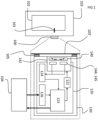
- the device consists of a number of different parts, as depicted in Figure 1 .
- This figure is a functional diagram of the sensor system 100, mounted on the meter cabinet 103 of a watt-hour meter 102, comprising a rotating disc 101.
- the meter cabinet 103 is for instance a transparent or translucent closet made of poly methyl methacrylate (PMMA), polycarbonate or a regular glass type.
- PMMA poly methyl methacrylate
- the sensor system 100 as being attached onto the outside meter cabinet wall 103', comprises of components and functionalities as indicated further within the dashed lines.
- a fixation mechanism 105 is provided in order to fulfill the attachment of the sensor system housing 130 onto the cabinet wall 103'.
- a PCB 120 and its electronic components is provided, as well as an optical system 142, comprising lenses 140 optionally including filters, and light emitters 144 and light receivers 145.
- the signal as captured by a light receiver 145 - and also in connection with the PCB 120, is transmitted for signal conditioning by a signal conditioning element 124 and further processing by means of a central processing unit or CPU 123.
- the CPU 123 is also in direct relation with a driver 121 connected with the PCB 120, for powering the light emitters 144 under control of the CPU 123.
- a bidirectional communication interface 126 connected with the PCB 120 and in direct relation to the CPU 123 allows the retrieval of information from the sensor system 100, like for instance power consumption or power production as well as to send information to the sensor module as for instance configuration parameters or upgrading the application of the CPU 123, with an externally connected device 104, also referred to as meter module.
- Information from the sensor system 100 like for instance power consumption or power production as well as to send information to the sensor module as for instance configuration parameters or upgrading the application of the CPU 123, with an externally connected device 104, also referred to as meter module.
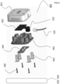
- FIG. 2 An exploded view of an embodiment of the sensor system 200 is presented in Figure 2 , as well as a meter 202 or meter cabinet 203 onto which the sensor system 200 can be mounted.
- This sensor system 200 as illustrated in Figure 2 comprises of the following parts: a cover 210 as part of the housing 130, a PCB 220 and mounted thereon a connector 222 and cable 225 to the meter module 104, an assembling part 230 of the housing 130, a lens plate 240, fixation brackets 250, and screws 260.
- the driver 121, nor the light emitters 144 and light receivers 145 are depicted here, but are mounted onto and connected with the PCB 220.
- the sensor system 100, 200 can be placed on any meter 102, 202 or meter cabinet 103, 203 presenting a flat transparent or translucent surface 103' that is large enough for the sensor system in front of the meter disc 101.
- the fixation mechanism 105 developed for this sensor system 100, 200 presents multiple advantages. It allows positioning the sensor system 100, 200 on a meter 102, 202 or meter cabinet 103, 203 without requiring any additional tool. It also makes it possible for a user to remove the sensor system 100, 200 while leaving the brackets 250 in their position. This allows an easy reading of the meter index without the sensor system 100, 200 being in the field of view.
- a further tool 1800 as shown in Figure 18 comparable with a housing cover in shape and size, and comprising a centralized cross-shaped viewing window 1801 is provided which holds the brackets 250 and allows them to be aligned with the disc 101. While Figure 18 (a) is depicting the front side of the tool 1800, i.e.
- Figure 18 (b) illustrates the backside of the tool 1800, meaning closer to the meter cabinet 103, 203, and moreover showing square-shaped parts of double-sided tape 1856, provided onto the brackets 1850 and being used to fix the brackets 1850 onto the meter cabinet 103, 203.
- the fixation mechanism 105 consists of four brackets 250, 350, 450, of which different views are illustrated in Figure 3 and 4 .
- the brackets 250, 350, 450 are held inside the housing 130, more particularly inside the assembling part 230 of the sensor system 100, 200 using a kind of snaps or clicking mechanism 351 with bumps and notches.
- Double-sided Very High Bond tape 456 is used to fix the brackets 250, 350, 450 onto the transparent surface 103', and to maintain these brackets 250, 350, 450 in their positions, as shown in Figure 4 .
- the surface provided with dual-sided tape is not completely arbitrary, but well-chosen, including the number of attached bracket surfaces are part of the design.
- brackets 250, 350, 450, 550 are held in position within the housing's assembling part 230, 530 - and enabled by means of a pin 531 - as described in Figure 5 .
- This allows the user to move the sensor system 100, 200 on the surface 103', 503' where it will be placed without having the tape 456 come into contact with the surface.
- the brackets 250, 350, 450, 550, 650 can be pressed against the surface 103', 603', as shown in Figure 6 . This makes the double-sided tape 456 on the bracket 250, 350, 450 come into contact with the meter 102, 202 or the meter cabinet 103, 203.
- the brackets 350 are for example provided with at least two bumps 352, 354 and adjacent notches 353, 355 in a longitudinal bracket rod 356.
- the system's housing assembling part 530 is for instance provided with a pin 531 matching in shape and size with either of the notches 553, 555 in the bracket 550.
- the bracket 550 can be retained in at least two positions: a first hold position of the housing's pin 531 in a first notch 555 can be used to facilitate correct positioning of the system 100, 200 to the mounting surface 503', illustrated in Figure 5 , whereas a second hold position of the housing's pin 631 in a second notch 653 can be used for pressing the bracket 650 against the mounting surface 603', as shown in Figure 6 .
- the pressing surface of the bracket 650 is provided with an adhesive such as dual-sided tape, the bracket 650 can be fixed to the mounting surface 603'.
- the bumps and notches may differ in size and/or shape.
- a thick large bump 654 is particularly chosen from pressing the bracket 650 against the mounting surface 603', applying a rather significant force to perform this; a small bump 652 is particularly designed to hold a certain position but also enable easy removal and re-attachment of the housing's assembling part 630 onto the bracket 650.
- the housing 130 of the sensor system 100, 200 consists of two main parts.
- a first black part 230 on the side of the meter 102, 202 holds the lenses 140, provided within a lens plate 240, the PCB 120, 220 and the four brackets 250.
- This assembling part 230 needs to be black to avoid internal reflections of the light from the light emitters 144, such as for instance LEDs to the light receivers 145 e.g. phototransistors, which could have a negative influence on the correct interpretation and functioning of the sensor system 100, 200.
- the second part or cover 210 is on the backside of the sensor system 100, 200 and mainly serves to close the sensor system housing 130, required to achieve the IP51 standard for the sensor system 100, 200 (related e.g. to water drops and dust free applications).
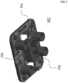
- Figures 7-10 show the assembling part 230, 730, 930 of the housing 130 in accordance with an embodiment of the invention.
- Figure 7 depicts the inner side of the assembling part 730 onto which the PCB is held in position by the snaps 701, particularly attaching, and the pins 702, particularly positioning.
- the inner side of the assembling part 230 is particularly oriented towards the housing's cover 210.
- a baffle 703 between the LEDs 144 and the phototransistors 145 is provided as physical barrier in order to reduce or eliminate internal reflections.
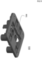
- the assembling part 730 provided with PCB 820 and connector 822 mounted thereon is shown in Figure 8 .
- Figure 9 shows the so-called outer side of the assembling part 930, i.e.
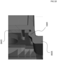
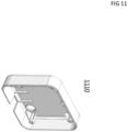
- FIG. 10 A perspective view of the cover part 1110 is presented in Figure 11 , for ensuring a water drops free and dust free system. Both housing parts are attached to each other using four screws 260 as described above referring to the exploded view of Figure 2 .
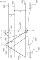
- the main challenge in the design of the optical system 142 is to provide all good signal quality over a distance d with big variable distance range from 0.5cm up to 10cm between the sensor system 1200 mounted onto the outer cabinet surface 1203 and the meter 1202 itself, without any adjustment to be made during installation, as depicted in Figure 12 (b) .
- a dashed line is drawn, being the perpendicular - leaving the disc centre X - to the disc peripheral edge part that is to be measured, and dividing the sensor system 1200 is a Left side and a Right side respectively.
- Figure 12 (c) is giving more detail (not drawn to scale) of the Right side of the optical system, particularly regarding the light emitters and light receivers, their corresponding optical elements and corresponding emitted and/or reflected light beams. Similar optics detail may be understood for the Left side of the sensor system. While referring also to Figure 12 (c) , the meter 1202, or more particularly the meter plate, for instance made of metal, may be provided with a meter glass 1202' put in front it, at a distance ⁇ measured from the meter plate, or at a distance ⁇ taken from the disc 1201 protruding from the meter plate.
- a distance d' is given here as being the distance with big variable distance range between the cabinet surface 1203 onto which the sensor system 1200 may be mounted, and the meter glass 1202' from the meter 1202 itself.
- the distances ⁇ and ⁇ are both variable.
- the distance ⁇ may be smaller than the distance ⁇ meaning that the disc 1201 is protruding from the meter plate, but according to another embodiment, the disc 1201 may be located more inwards in the meter 1202, and therefor it is possible also that the distance ⁇ becomes equal or larger than the distance ⁇ .
- the meter glass 1202' and/or the cabinet surface 1203 may be made of an optical medium such as PMMA or polycarbonate, possibly coloured or darkened, or otherwise treated.
- the refraction of light passing such an optical medium is negligible as compared to the throughput beam of the emitted and reflected light. Although there is a particular loss of signal due to the existence of an optical medium, this will eventually not effect the interpretation of the resulting signal by the sensor system.
- the disc 1201 with the mark 1212 and center X can vary in reflective property from very shiny over matt to corrugate. The designed optical system can cope with all these influences without any adjustments.
- the light source chosen is a LED 1207.
- the LED 1207 is projecting light to the disc 1201 in a parallel beam 1209 by means of a first type of lens 1205.
- the beam 1209 is perpendicular to the meter 1202, meter glass 1202' or meter cabinet surface 1203, to avoid reflections on the (glass) window of the meter 1202 or meter cabinet 1203 directly into the receiving phototransistor 1206.
- the light reflected 1211 by the peripheral edge of the disc 1201 is captured by a phototransistor 1206 after having passed a second type of lens 1204, having a field of view 1210 characterized by an angle ⁇ .
- this phototransistor lens 1204 only manipulates the beam in a vertical direction, i.e. along a direction perpendicular to the meter disc 101. Hence with the horizontal plane or within a certain horizontal range of measurement, the angle ⁇ is not transformed by the lens 1204 and thus angle ⁇ may be considered equal to angle ⁇ ' characterising the field of the phototransistor 1206 itself. Moreover, while referring to Left side and Right side of the sensor system, two LED lenses 1205 and two phototransistor lenses 1204 are installed with corresponding LEDs 1207 and phototransistors 1205.
- one LED lens 1205 and one phototransistor lens 1204 are on the Left side, and one of each are provided on the Right side, including corresponding light emitters 1207 and receivers 1206.
- This specific optical set-up with a LED/phototransistor Left side and a LED/phototransistor Right side respectively is chosen in order to not only measure a change or mark 1212 on the moving disc 1201, but also enabling the sensor system 1200 to detect the direction of rotation of the moving disc 1201.
- the distances L1 and L2 in Figure 12 (a) and (c) are measured from the perpendicular line of the center of the disc peripheral edge part to be measured, i.e. the dotted line outgoing the disc center X, towards the center of the LED 1207 or towards the center of the phototransistor 1206 respectively.
- the distances L1 and L2 are optimized to capture a good signal despite all the variables such as distance range, disc diameter and thickness, disc reflective properties, transparency and color of the meter cabinet without any adjustment required.
- the peripheral edge of the disc 1201 may be ribbed, or either a glossy surface. In this latter case, the reflected beam will be stronger and more directed, and hence the positioning of the lenses, or in other words the accuracy of the distances L1 and L2 becomes more critical.
- the lens plate is a single PMMA (e.g. Plexiglas) piece, made by means of injection molding, that includes four separate lenses: two for the LEDs 1207 and two for the phototransistors 1206.
- the PMMA material is for instance chosen because of the compromise or trade off between manufacturability and functionality.
- Figure 13 shows the lens plate 1300, with the indicated lenses 1304, 1305.
- the central, cylindrical lenses 1305 are for the LEDs 1207 while the outside ones 1304 are for the phototransistors 1206.
- Snap recesses 1301 are foreseen in the lens plate 1300 to be positioned beneath the snaps of the housing, whereas openings 1302 between outer lenses 1304 and the rest of the plate 1300 are made to avoid internal reflection of LED light to the phototransistor lenses 1304.
- Each lens 1304, 1305 is specifically designed for a sensor system 1200 (see also 100, 200 in Figure 1 and 2 ) according to the present invention.
- the LED lenses 1305 are cylindrical lenses that lead to a focused light beam creating a circular spot of 8-10 mm diameter. These lenses 1305 are designed as Fresnel lenses to avoid having a plastic part too thick to mold without issue.
- the small opening angle of the emitted light beam from the LEDs 1207 allows the sensor system 1200 to be used at a distance d or d' with large variable range to the meter, whereas the size of the spot does not change significantly with the distance.
- the phototransistors 1206 are replaced by red colored LEDs to provide a visualization of the optical alignment between emitter and receiver, as illustrated by the dashed line.
- the indicated spots 1401 are red colored.
- the lenses 1304 for the phototransistors 1206 are oriented or pivoted slightly towards the center of the disc, maximizing the amount of LED light reflected to the phototransistors. In Figure 1 this is schematically illustrated - yet in an exaggerated way - by the outer lines drawn within the box representing the lenses 140 of the sensor system 100.
- the LED light spots are not focused on the disc 1201 itself but at infinity and the emitted beams 1209 are parallel to each other and perpendicular to the meter 1202. This creates two spots of constant size, independent of the distance between the sensor system 1200 and the disc 1201, further enabling the sensor system 1200 to be used at over a large distance range from 0.5 to 10 cm from the meter 1202.
- the PCB and its components rely on state-of-the-art existing and standard available material, i.e. not adapted or customized, although particular components, such as the LEDs and the phototransistors for example are particularly chosen according to an embodiment of the invention.
- each step will be described in the logical order for the signal processing.
- the steps of 'Signal generation' up to 'Mark detection' are performed in both signal channels independently, whereas each signal is captured by one of the phototransistors in a predetermined way, i.e. Left signal is captured by Left side phototransistor, and Right signal is captured by Right side phototransistor.
- the step of 'Rotation detection' requires the results of both signals (Left and Right) processed together to perform correctly.
- the LEDs are for example selected as emitting light within the visible spectrum, except using e.g. the color red while the mark on a watt-hour meter disc is often colored red (instead of common black).
- red infrared LED light
- the signal is for instance generated by two blue LEDs projecting light onto the meter disc.
- Each LED is modulated at a frequency of 1kHz, for example for a 25% on and 75% off status. The blue light was chosen to ensure that it is absorbed by all black and red marks or stripes on the meter disc.
- the modulation frequency was selected to make a clear distinction between the intended LED light and the unwanted ambient light coming from many possible types of light sources present in households, such as for instance incandescent light bulbs, LED lamps, halogen lamps, neon tubes, fluocompact lamps and HID lamps. This method is also used to make a clear distinction between the intended LED light and the unwanted light originating from exposure to sunlight. Moreover, light sources of 300 à 400 Hz may cause flicker due to on/off pulsation, whereas modulated or pulsed light is generally preferred for avoiding noise and disturbances. A frequency significantly above the 300-400 Hz range is chosen in order to avoid flicker, and therefor the LED is modulated at 1kHz frequency.
- both LEDs are identical in shape but are shifted over 2t in time (4t being the period of the signal). Crosstalk is herewith avoided.
- the signals used for the rest of the processing are the ones obtained by phototransistors, and a 24-bit ADC at a sampling frequency of 24 kHz. While respecting the Nyquist formula, this implies that for every signal channel 24.000 measuring points per second are generated, whereas each sample point corresponding with particular amplitude is translated and stored into a 24-bit representation within the central processing unit or CPU. Due to the 24-bit representation, a total of 2 24 possible values or levels can be identified for the analysis of amplitude spectra of the captured signals, and hence considering the environmental light many different light signals on different levels of e.g. brightness, and/or intensity can be added, even though they are not important, and will eventually not effect the final result. The resolution of the ADC was chosen to ensure a sufficient resolution in all situations from dark environments to direct sunlight.
- a 10-bit ADC is used to sample the operating point of the phototransistor, after making use e.g. its sensitivity curve in order to transfer all captured signal parts to a sort of leveling out while bringing them on a curve with comparable signal strength. This allows for gain compensation of the phototransistor with respect to ambient light intensity, effectively suppressing signal level variations of the measured LED light intensity, hence providing a more robust and reliable system. A correction for normalization of the signal is thus performed.
- the 10-bit is chosen arbitrary, meaning that other logical variants are also possible to consider.
- the signal obtained from the 24-bit ADC is processed through the following steps:
- the occurrence of the mark on the disc in front of the sensor system can be detected as a dip in the signal intensity, created by the higher absorption of light by the black or red mark compared to the rest of the disc.
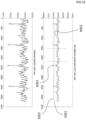
- the mark detection is performed using two thresholds 1501, 1502 as illustrated in Figure 15 , the signal having to pass under the lower one and come back above the higher one for a mark to be detected.
- the thresholds are defined during the calibration procedure as described below.
- absolute minimum 1503 and local dip 1504 are determined for defining the thresholds 1501, 1502 to be used for mark detection and signal calibration.
- the first threshold 1501 is e.g. chosen at 45% below the local dip 1504, whereas the second threshold 1502 is e.g. defined as 45% above the absolute minimum 1503.
- the range between both threshold values 1501, 1502 represents the left over 10%.
- the thresholds are constantly updated to keep up with any change in signal amplitude due to temperature changes and component degradation.
- the algorithm makes full use of the marks detected by the two sensors.
- a pulse is only accounted for once a mark has been detected by both sensors: a positive pulse (energy consumption is larger than possible energy production) if a mark is detected on the left phototransistor subsequently followed by the right phototransistor and a negative pulse (energy production is larger than energy consumption) in the inverse case.
- the algorithm is also robust against a missed mark in either signal, correcting itself automatically by adding two pulses if required.
- the first step during installation of the sensor system is the correct positioning of the sensor system in front of the meter disc. This can be done using the two LED spots. These spots must be focused on the disc and placed symmetrically left and right of the center of the disc. Once the position has been determined using the LED light spots, the four brackets can be pressed against the cabinet, and hence fixed as described above.
- the sensor system calibration is related to the definition of the thresholds as described above. This calibration is performed automatically after powering on of the sensor system. Hence, this means both after an installation by the installer and as recovery method after a power down of the sensor system. Note that the following detail about the procedure is independently executed for each signal channel.
- the calibration method comprises two parts: a bootstrap algorithm providing a first rough version of the thresholds, and a refinement phase, refining and/or updating these thresholds to get the highest possible immunity to noise and signal drift.
- the refinement phase never ends, i.e. it continues adapting the thresholds during the life of the sensor system.
- thresholds On sensor system start-up, no valid thresholds are known. To come to a first version of these thresholds, the algorithm keeps track of the minimum and the average of the signal. The thresholds are continuously redefined between these two evolving measurements. At the same time, these thresholds are used to detect dips in the signal. When a dip is detected, its minimum is recorded. When the last five recorded minima are close enough together and rather far away from all the other measured points, the bootstrap phase is considered to be successful and the controller continues with the refinement phase. Numerous extra checks are in place to prevent premature bootstrapping on a disc that is not moving.
- the minimum of every dip and the minimum between two dips are measured and subsequently used to each update and exponential moving average.
- These slowly-adapting versions are used to update the thresholds. This way, the thresholds evolve along with any drift due to aging or thermal influences.
- the sensor provides feedback to the external metering module and hence to the installer after a successful calibration.
- the sensor can easily be removed from the meter, leaving only the four brackets in place. This allows for an easier reading of the meter index.
- the sensor system is robust against such use and will continue working normally and as before, once put back in clicked mounted position.
Landscapes
- Physics & Mathematics (AREA)
- General Physics & Mathematics (AREA)
- Length Measuring Devices By Optical Means (AREA)
Description
- The invention relates to systems and methods for detecting a change on a moving surface, such as for instance a rotating disc, provided with a mark, of an electricity meter.
- The consumption measured by an electricity meter with a rotating disc can be derived from the number of rotations of the disc, counted or calculated by marking the disc with a dot or image, and hence indicating a full rotation. The following problems are identified in the field of sensors for detecting the rotation of a disc with an indicator mark in an electric power meter:
- No possible use of state-of-the-art sensors or sensor systems at a largely variable distance from an electricity meter. Moreover, further difficulties in detection are observed when the watt-hour meter is enclosed in a transparent/translucent cabinet, in addition to the glass housing of the meter.
- Disturbing effect of ambient light - variable from dark at night to very bright artificial lamps or direct sunlight.
- Installing of a sensor requires particular technical handling for initiating the detection.
- Sensor is disabling visibility of the utility meter: one can no longer look at the details of the electricity meter when the sensor is mounted for detection. The sensor is either fixed or devious in removing and/or reinstalling. Moreover, when reinstalling the exact positioning from previous set-up cannot be achieved.
-
EP 2 950 053 provides a device for detecting a change on a moving surface with at least one light generating device for generating light to be directed to said moving surface; and at least one light sensor for capturing reflected light from said moving surface; wherein said change on said moving surface, is detected based on said reflected light captured by said light sensor, but since the source and detectors are not lying in the plane of movement of the moving surface, this device does not resolve all of the aforementioned problems. - There is a need for a solution for the above stated problems.
- The invention aims at providing systems and methods for detecting a change on a moving surface which can be applied at a fairly variable distance while achieving the same final output, to be used at any ambient light conditions, and comprising an automatic self-learning or self-adapting calibration, in an easily removable and reproducible way.
- The present invention is set out in the appended set of claims.
-
-
Figure 1 schematically shows the functional diagram of a sensor system in an application set-up in accordance with an embodiment of the present invention. -
Figure 2 illustrates an exploded view of the sensor system according to an embodiment of the present invention. -
Figure 3 and 4 illustrate the bracket in different views in accordance with an embodiment of the present invention. -
Figure 5 illustrates the hold position of the bracket according to an embodiment of the present invention. -
Figure 6 illustrates the pressed position of the bracket according to an embodiment of the present invention. -
Figure 7 illustrates one side the assembling part of the housing in accordance with an embodiment of the present invention. -
Figure 8 illustrates the other side of assembling part of the housing provided with PCB and connector in accordance with an embodiment of the present invention. -
Figure 9 illustrates the assembling part of the housing in accordance with an embodiment of the present invention. -
Figure 10 shows detail of the undercut snap depicted inFigure 9 . -
Figure 11 illustrates the cover of the housing according to an embodiment of the invention. -
Figure 12 (a) and(b) illustrate the optical concept according to the present invention. -
Figure 13 illustrates the lens plate and its lenses according to an embodiment of the present invention. -
Figure 14 illustrates the optical alignment of emitter and receiver according an embodiment of the present invention. -
Figure 15 illustrates the dip detection and determination of thresholds in accordance with an embodiment of the present invention. -
Figure 16 illustrates the modulated LED light sources according to an embodiment of the invention. -
Figure 17 is a schematic representation of a Chebyshev bandpass filter used according to an embodiment of the invention. -
Figure 18 illustrates (a) front and (b) backside of an alignment tool used for positioning the brackets according to an embodiment of the invention. - A sensor system as defined in the appended set of claims, is designed to be mounted on an electricity meter or its cabinet and optically detect the rotations of the meter disc. Rotations are detected by directing the light of two LEDs on the disc, and detecting the occurrence of the black or red mark on the disc by the sharp change or decrease in reflected light it causes, captured by two phototransistors. Two sets of LED and phototransistor are used to make the sensor system able to detect not only the rotations of the disc but also its rotation direction.
- The sensor system as defined in the appended set of claims, processes the data from the phototransistors internally to obtain the necessary information about the rotation of the meter disc. Once a rotation has been detected, a pulse is sent to the meter module. A register of the total number of rotations is also kept internally so that a meter module system can consult it if necessary.
- Each part of the sensor system is described in detail below:
- Fixation mechanism
- Housing
- Optical system
- PCB and components
- Algorithms and processing
- Moreover, installation and use of the sensor system is particularly described in subsequent paragraphs.
- Finally, an overview is given of the challenges overcome by means of the present invention.
- According to an embodiment of the invention, the device consists of a number of different parts, as depicted in
Figure 1 . This figure is a functional diagram of thesensor system 100, mounted on themeter cabinet 103 of a watt-hour meter 102, comprising a rotatingdisc 101. Themeter cabinet 103 is for instance a transparent or translucent closet made of poly methyl methacrylate (PMMA), polycarbonate or a regular glass type. More into detail, thesensor system 100 as being attached onto the outside meter cabinet wall 103', comprises of components and functionalities as indicated further within the dashed lines. For instance, afixation mechanism 105 is provided in order to fulfill the attachment of the sensor system housing 130 onto the cabinet wall 103'. Within thehousing 130, aPCB 120 and its electronic components is provided, as well as anoptical system 142, comprisinglenses 140 optionally including filters, and light emitters 144 and light receivers 145. The signal as captured by a light receiver 145 - and also in connection with thePCB 120, is transmitted for signal conditioning by asignal conditioning element 124 and further processing by means of a central processing unit orCPU 123. TheCPU 123 is also in direct relation with adriver 121 connected with thePCB 120, for powering the light emitters 144 under control of theCPU 123. Abidirectional communication interface 126 connected with thePCB 120 and in direct relation to theCPU 123 allows the retrieval of information from thesensor system 100, like for instance power consumption or power production as well as to send information to the sensor module as for instance configuration parameters or upgrading the application of theCPU 123, with an externally connecteddevice 104, also referred to as meter module. Pictures and more detailed schematics will be referred to later on, when discussing specific parts of this diagram. - An exploded view of an embodiment of the
sensor system 200 is presented inFigure 2 , as well as a meter 202 or meter cabinet 203 onto which thesensor system 200 can be mounted. Thissensor system 200 as illustrated inFigure 2 comprises of the following parts: acover 210 as part of thehousing 130, aPCB 220 and mounted thereon aconnector 222 andcable 225 to themeter module 104, an assemblingpart 230 of thehousing 130, alens plate 240,fixation brackets 250, andscrews 260. Nor thedriver 121, nor the light emitters 144 and light receivers 145 are depicted here, but are mounted onto and connected with thePCB 220. - In accordance with an embodiment of the invention, the
sensor system meter 102, 202 ormeter cabinet 103, 203 presenting a flat transparent or translucent surface 103' that is large enough for the sensor system in front of themeter disc 101. Thefixation mechanism 105 developed for thissensor system sensor system meter 102, 202 ormeter cabinet 103, 203 without requiring any additional tool. It also makes it possible for a user to remove thesensor system brackets 250 in their position. This allows an easy reading of the meter index without thesensor system sensor system brackets 250 that were left on themeter 102, 202 or thecabinet 103, 203. According to an alternative embodiment, for example in case there is limited view of thedisc 101 within themeter 102, 202 ormeter cabinet 103, 203, making alignment of thesensor system disc 101 difficult or rather impossible, afurther tool 1800 as shown inFigure 18 , comparable with a housing cover in shape and size, and comprising a centralizedcross-shaped viewing window 1801 is provided which holds thebrackets 250 and allows them to be aligned with thedisc 101. WhileFigure 18 (a) is depicting the front side of thetool 1800, i.e. further away from themeter cabinet 103, 203 onto which thebrackets 1850 are mounted,Figure 18 (b) illustrates the backside of thetool 1800, meaning closer to themeter cabinet 103, 203, and moreover showing square-shaped parts of double-sided tape 1856, provided onto thebrackets 1850 and being used to fix thebrackets 1850 onto themeter cabinet 103, 203. - The
fixation mechanism 105 consists of fourbrackets Figure 3 and 4 . Thebrackets housing 130, more particularly inside the assemblingpart 230 of thesensor system mechanism 351 with bumps and notches. Double-sided VeryHigh Bond tape 456 is used to fix thebrackets brackets Figure 4 . According to an embodiment of the invention, the surface provided with dual-sided tape, is not completely arbitrary, but well-chosen, including the number of attached bracket surfaces are part of the design. It appears to be that a particular surface for attachment is better divided into four respective smaller mounting areas rather than concentrating the attachment surface to a single large area. In a first instance, thebrackets part 230, 530 - and enabled by means of a pin 531 - as described inFigure 5 . This allows the user to move thesensor system tape 456 come into contact with the surface. Once thesensor system brackets Figure 6 . This makes the double-sided tape 456 on thebracket meter 102, 202 or themeter cabinet 103, 203. - Further referring to
Figure 3 , thebrackets 350 are for example provided with at least twobumps adjacent notches longitudinal bracket rod 356. Referring again toFigure 5 , the system'shousing assembling part 530 is for instance provided with apin 531 matching in shape and size with either of thenotches bracket 550. Hence, thebracket 550 can be retained in at least two positions: a first hold position of the housing'spin 531 in afirst notch 555 can be used to facilitate correct positioning of thesystem Figure 5 , whereas a second hold position of the housing'spin 631 in asecond notch 653 can be used for pressing thebracket 650 against the mounting surface 603', as shown inFigure 6 . Furthermore, when the pressing surface of thebracket 650 is provided with an adhesive such as dual-sided tape, thebracket 650 can be fixed to the mounting surface 603'. According to an embodiment of the invention, the bumps and notches may differ in size and/or shape. As depicted for example inFigure 6 , a thicklarge bump 654 is particularly chosen from pressing thebracket 650 against the mounting surface 603', applying a rather significant force to perform this; asmall bump 652 is particularly designed to hold a certain position but also enable easy removal and re-attachment of the housing's assemblingpart 630 onto thebracket 650. - While referring again to
Figure 1 and2 , according to an embodiment of the invention, thehousing 130 of thesensor system black part 230 on the side of themeter 102, 202 holds thelenses 140, provided within alens plate 240, thePCB brackets 250. This assemblingpart 230 needs to be black to avoid internal reflections of the light from the light emitters 144, such as for instance LEDs to the light receivers 145 e.g. phototransistors, which could have a negative influence on the correct interpretation and functioning of thesensor system sensor system sensor system housing 130, required to achieve the IP51 standard for thesensor system 100, 200 (related e.g. to water drops and dust free applications). -
Figures 7-10 show the assemblingpart housing 130 in accordance with an embodiment of the invention.Figure 7 depicts the inner side of the assemblingpart 730 onto which the PCB is held in position by thesnaps 701, particularly attaching, and thepins 702, particularly positioning. As clearly shown inFigure 2 , the inner side of the assemblingpart 230 is particularly oriented towards the housing'scover 210. Abaffle 703 between the LEDs 144 and the phototransistors 145 is provided as physical barrier in order to reduce or eliminate internal reflections. The assemblingpart 730 provided withPCB 820 andconnector 822 mounted thereon is shown inFigure 8 .Figure 9 shows the so-called outer side of the assemblingpart 930, i.e. the side that is oriented to themeter disc 101. By means of asnap 901 thelens plate 240 as illustrated inFigure 2 is positioned and fixed. This is shown in a more detailed way inFigure 10 , wherein thelens plate 1040 is mounted onto the assemblingpart 1030 and moreover fixed by means of thesnap 1001. A perspective view of thecover part 1110 is presented inFigure 11 , for ensuring a water drops free and dust free system. Both housing parts are attached to each other using fourscrews 260 as described above referring to the exploded view ofFigure 2 . - According to an embodiment of the invention, the main challenge in the design of the
optical system 142 is to provide all good signal quality over a distance d with big variable distance range from 0.5cm up to 10cm between thesensor system 1200 mounted onto theouter cabinet surface 1203 and themeter 1202 itself, without any adjustment to be made during installation, as depicted inFigure 12 (b) . Further in this Figure, a dashed line is drawn, being the perpendicular - leaving the disc centre X - to the disc peripheral edge part that is to be measured, and dividing thesensor system 1200 is a Left side and a Right side respectively.Figure 12 (c) is giving more detail (not drawn to scale) of the Right side of the optical system, particularly regarding the light emitters and light receivers, their corresponding optical elements and corresponding emitted and/or reflected light beams. Similar optics detail may be understood for the Left side of the sensor system. While referring also toFigure 12 (c) , themeter 1202, or more particularly the meter plate, for instance made of metal, may be provided with a meter glass 1202' put in front it, at a distance Δ measured from the meter plate, or at a distance δ taken from thedisc 1201 protruding from the meter plate. Hence, a distance d' is given here as being the distance with big variable distance range between thecabinet surface 1203 onto which thesensor system 1200 may be mounted, and the meter glass 1202' from themeter 1202 itself. The distances Δ and δ are both variable. The distance δ may be smaller than the distance Δ meaning that thedisc 1201 is protruding from the meter plate, but according to another embodiment, thedisc 1201 may be located more inwards in themeter 1202, and therefor it is possible also that the distance δ becomes equal or larger than the distance Δ. The meter glass 1202' and/or thecabinet surface 1203 may be made of an optical medium such as PMMA or polycarbonate, possibly coloured or darkened, or otherwise treated. The refraction of light passing such an optical medium is negligible as compared to the throughput beam of the emitted and reflected light. Although there is a particular loss of signal due to the existence of an optical medium, this will eventually not effect the interpretation of the resulting signal by the sensor system. Thedisc 1201 with themark 1212 and center X can vary in reflective property from very shiny over matt to corrugate. The designed optical system can cope with all these influences without any adjustments. - This is achieved by the optical concept as illustrated in
Figure 12 (a) ,(b) and(c) in accordance with an embodiment of the present invention. The light source chosen is aLED 1207. TheLED 1207 is projecting light to thedisc 1201 in aparallel beam 1209 by means of a first type oflens 1205. Thebeam 1209 is perpendicular to themeter 1202, meter glass 1202' ormeter cabinet surface 1203, to avoid reflections on the (glass) window of themeter 1202 ormeter cabinet 1203 directly into the receivingphototransistor 1206. The light reflected 1211 by the peripheral edge of thedisc 1201 is captured by aphototransistor 1206 after having passed a second type oflens 1204, having a field ofview 1210 characterized by an angle α. According to an embodiment of the invention, thisphototransistor lens 1204 only manipulates the beam in a vertical direction, i.e. along a direction perpendicular to themeter disc 101. Hence with the horizontal plane or within a certain horizontal range of measurement, the angle α is not transformed by thelens 1204 and thus angle α may be considered equal to angle α' characterising the field of thephototransistor 1206 itself. Moreover, while referring to Left side and Right side of the sensor system, twoLED lenses 1205 and twophototransistor lenses 1204 are installed withcorresponding LEDs 1207 andphototransistors 1205. More particularly, oneLED lens 1205 and onephototransistor lens 1204 are on the Left side, and one of each are provided on the Right side, including correspondinglight emitters 1207 andreceivers 1206. This specific optical set-up with a LED/phototransistor Left side and a LED/phototransistor Right side respectively is chosen in order to not only measure a change or mark 1212 on the movingdisc 1201, but also enabling thesensor system 1200 to detect the direction of rotation of the movingdisc 1201. The distances L1 and L2 inFigure 12 (a) and(c) are measured from the perpendicular line of the center of the disc peripheral edge part to be measured, i.e. the dotted line outgoing the disc center X, towards the center of theLED 1207 or towards the center of thephototransistor 1206 respectively. - Considering the field of view of the
phototransistor lenses 1204, and/or of thephototransistors 1206, the distances L1 and L2 are optimized to capture a good signal despite all the variables such as distance range, disc diameter and thickness, disc reflective properties, transparency and color of the meter cabinet without any adjustment required. The peripheral edge of thedisc 1201 may be ribbed, or either a glossy surface. In this latter case, the reflected beam will be stronger and more directed, and hence the positioning of the lenses, or in other words the accuracy of the distances L1 and L2 becomes more critical. - According to an embodiment of the invention, there is a particular relation between the distance of the LED L1, and the distance of the phototransistor L2 to the perpendicular from the disc centre X on one hand, and the field of view characterizing angle α of the phototransistor lens, and the field of view characterizing angle α' of the phototransistor on the other hand, such that there is always an overlap between the LED spots and the field of view of the phototransistor. Whereas α ≅ α' within a horizontal range as mentioned above, further referring to
Figure 12 (c) , the following formula may be applied:
- with 15 cm ≥ d' ≥ 0,2 cm, preferably 10 cm ≥ d' ≥ 0,5 cm;
- and 5 cm ≥ δ ≥ 0 cm, preferably 1 cm ≥ δ ≥ 0,1 cm
- and dlp being the distance between the
meter cabinet 1203 and thelens plate 1220 of thesensor system 1200, whereas for example 15mm ≥ dlp ≥ 1mm, preferably 10mm ≥ dlp ≥ 2mm - and L1 is approximately 5mm, given the diameter of the LED lens is about 15mm, and the width of the phototransistor lens is about 12mm.
- According to an embodiment of the present invention, the lens plate is a single PMMA (e.g. Plexiglas) piece, made by means of injection molding, that includes four separate lenses: two for the
LEDs 1207 and two for thephototransistors 1206. The PMMA material is for instance chosen because of the compromise or trade off between manufacturability and functionality.Figure 13 shows thelens plate 1300, with the indicatedlenses cylindrical lenses 1305 are for theLEDs 1207 while theoutside ones 1304 are for thephototransistors 1206. Snap recesses 1301 are foreseen in thelens plate 1300 to be positioned beneath the snaps of the housing, whereasopenings 1302 betweenouter lenses 1304 and the rest of theplate 1300 are made to avoid internal reflection of LED light to thephototransistor lenses 1304. - Each
lens Figure 1 and2 ) according to the present invention. TheLED lenses 1305 are cylindrical lenses that lead to a focused light beam creating a circular spot of 8-10 mm diameter. Theselenses 1305 are designed as Fresnel lenses to avoid having a plastic part too thick to mold without issue. The small opening angle of the emitted light beam from theLEDs 1207 allows thesensor system 1200 to be used at a distance d or d' with large variable range to the meter, whereas the size of the spot does not change significantly with the distance. Thephototransistor lenses 1304, also designed as Fresnel lenses, focus the field of view of eachphototransistor 1206 to a horizontal line of a certain thickness or ellipse-alike view, as shown inFigure 14 . For this picture, thephototransistors 1206 are replaced by red colored LEDs to provide a visualization of the optical alignment between emitter and receiver, as illustrated by the dashed line. The indicatedspots 1401 are red colored. Thelenses 1304 for thephototransistors 1206 are oriented or pivoted slightly towards the center of the disc, maximizing the amount of LED light reflected to the phototransistors. InFigure 1 this is schematically illustrated - yet in an exaggerated way - by the outer lines drawn within the box representing thelenses 140 of thesensor system 100. - The LED light spots are not focused on the
disc 1201 itself but at infinity and the emittedbeams 1209 are parallel to each other and perpendicular to themeter 1202. This creates two spots of constant size, independent of the distance between thesensor system 1200 and thedisc 1201, further enabling thesensor system 1200 to be used at over a large distance range from 0.5 to 10 cm from themeter 1202. - The PCB and its components rely on state-of-the-art existing and standard available material, i.e. not adapted or customized, although particular components, such as the LEDs and the phototransistors for example are particularly chosen according to an embodiment of the invention.
- Due to the large number of operations to be described in this section, each step will be described in the logical order for the signal processing. In accordance with an embodiment of the invention, the steps of 'Signal generation' up to 'Mark detection' as mentioned below, are performed in both signal channels independently, whereas each signal is captured by one of the phototransistors in a predetermined way, i.e. Left signal is captured by Left side phototransistor, and Right signal is captured by Right side phototransistor. The step of 'Rotation detection' requires the results of both signals (Left and Right) processed together to perform correctly.
- According to an embodiment of the invention, the LEDs are for example selected as emitting light within the visible spectrum, except using e.g. the color red while the mark on a watt-hour meter disc is often colored red (instead of common black). In particular, infrared LED light is not preferred, whereas existing coatings in the field often reflect infrared light, and therefor may cause disturbing noise on the signals captured by the sensor system. As a result, the signal is for instance generated by two blue LEDs projecting light onto the meter disc. Each LED is modulated at a frequency of 1kHz, for example for a 25% on and 75% off status. The blue light was chosen to ensure that it is absorbed by all black and red marks or stripes on the meter disc. The modulation frequency was selected to make a clear distinction between the intended LED light and the unwanted ambient light coming from many possible types of light sources present in households, such as for instance incandescent light bulbs, LED lamps, halogen lamps, neon tubes, fluocompact lamps and HID lamps. This method is also used to make a clear distinction between the intended LED light and the unwanted light originating from exposure to sunlight. Moreover, light sources of 300 à 400 Hz may cause flicker due to on/off pulsation, whereas modulated or pulsed light is generally preferred for avoiding noise and disturbances. A frequency significantly above the 300-400 Hz range is chosen in order to avoid flicker, and therefor the LED is modulated at 1kHz frequency.
- Further referring to the presence of two LEDs, it is mentioned that their on/off status schedules differ amongst each other. As shown in
Figure 16 , the pulse interval of both LEDs doesn't coincide, but the pulse of LED2 appears one time interval later than the pulse of the LED1 sequence. According to an embodiment of the invention, a particular symmetry and synchronization between both LED light pulses is applied for an improved working of the sensor system. Both LED1 and LED2 signals are identical in shape but are shifted over 2t in time (4t being the period of the signal). Crosstalk is herewith avoided. - The signals used for the rest of the processing are the ones obtained by phototransistors, and a 24-bit ADC at a sampling frequency of 24 kHz. While respecting the Nyquist formula, this implies that for every signal channel 24.000 measuring points per second are generated, whereas each sample point corresponding with particular amplitude is translated and stored into a 24-bit representation within the central processing unit or CPU. Due to the 24-bit representation, a total of 224 possible values or levels can be identified for the analysis of amplitude spectra of the captured signals, and hence considering the environmental light many different light signals on different levels of e.g. brightness, and/or intensity can be added, even though they are not important, and will eventually not effect the final result. The resolution of the ADC was chosen to ensure a sufficient resolution in all situations from dark environments to direct sunlight.
- Although the signal is AC coupled, a 10-bit ADC is used to sample the operating point of the phototransistor, after making use e.g. its sensitivity curve in order to transfer all captured signal parts to a sort of leveling out while bringing them on a curve with comparable signal strength. This allows for gain compensation of the phototransistor with respect to ambient light intensity, effectively suppressing signal level variations of the measured LED light intensity, hence providing a more robust and reliable system. A correction for normalization of the signal is thus performed. The 10-bit is chosen arbitrary, meaning that other logical variants are also possible to consider.
- The signal obtained from the 24-bit ADC is processed through the following steps:
- 1. The signal is fed through a digital Chebyshev bandpass filter, centered at the 1kHz modulation frequency as illustrated in
Figure 17 wherein c is e.g. 5 Hz. By doing so, the intended LED light is retrieved and distinguished from the ambient light sources. - 2. The filtered signal is compensated for changes in sensitivity of the phototransistor due to ambient light fluctuations, using the also-sampled operating point. A calibration curve was measured and is saved on the controller.
- 3. After compensation, the signal is rectified and the envelope gets detected. In this process, the signal sampling frequency is also lowered, to for
instance 200 Hz, in order to reduce the processor load, while still having enough critical data or signal information for performing an accurate measurement analysis. - Once the envelope of the signal has been computed, the occurrence of the mark on the disc in front of the sensor system can be detected as a dip in the signal intensity, created by the higher absorption of light by the black or red mark compared to the rest of the disc. The mark detection is performed using two
thresholds Figure 15 , the signal having to pass under the lower one and come back above the higher one for a mark to be detected. The thresholds are defined during the calibration procedure as described below. According to an embodiment, absolute minimum 1503 andlocal dip 1504 are determined for defining thethresholds first threshold 1501 is e.g. chosen at 45% below thelocal dip 1504, whereas thesecond threshold 1502 is e.g. defined as 45% above the absolute minimum 1503. Hence the range between boththreshold values - To define whether a pulse must be sent out to the meter module, signaling a full rotation of the disc, the algorithm makes full use of the marks detected by the two sensors. A pulse is only accounted for once a mark has been detected by both sensors: a positive pulse (energy consumption is larger than possible energy production) if a mark is detected on the left phototransistor subsequently followed by the right phototransistor and a negative pulse (energy production is larger than energy consumption) in the inverse case.
- The algorithm is also robust against a missed mark in either signal, correcting itself automatically by adding two pulses if required.
- Changes of direction caused by the transition from consumption to production or reciprocally are also correctly detected thanks to the algorithm taking both signals into account before making a decision on the pulse to be sent out.
- The first step during installation of the sensor system is the correct positioning of the sensor system in front of the meter disc. This can be done using the two LED spots. These spots must be focused on the disc and placed symmetrically left and right of the center of the disc. Once the position has been determined using the LED light spots, the four brackets can be pressed against the cabinet, and hence fixed as described above.
- The sensor system calibration is related to the definition of the thresholds as described above. This calibration is performed automatically after powering on of the sensor system. Hence, this means both after an installation by the installer and as recovery method after a power down of the sensor system. Note that the following detail about the procedure is independently executed for each signal channel.
- The calibration method comprises two parts: a bootstrap algorithm providing a first rough version of the thresholds, and a refinement phase, refining and/or updating these thresholds to get the highest possible immunity to noise and signal drift. According to an embodiment, the refinement phase never ends, i.e. it continues adapting the thresholds during the life of the sensor system.
- On sensor system start-up, no valid thresholds are known. To come to a first version of these thresholds, the algorithm keeps track of the minimum and the average of the signal. The thresholds are continuously redefined between these two evolving measurements. At the same time, these thresholds are used to detect dips in the signal. When a dip is detected, its minimum is recorded. When the last five recorded minima are close enough together and rather far away from all the other measured points, the bootstrap phase is considered to be successful and the controller continues with the refinement phase. Numerous extra checks are in place to prevent premature bootstrapping on a disc that is not moving.
- In the refinement phase, the minimum of every dip and the minimum between two dips are measured and subsequently used to each update and exponential moving average. These slowly-adapting versions are used to update the thresholds. This way, the thresholds evolve along with any drift due to aging or thermal influences.
- The sensor provides feedback to the external metering module and hence to the installer after a successful calibration.
- The sensor can easily be removed from the meter, leaving only the four brackets in place. This allows for an easier reading of the meter index. The sensor system is robust against such use and will continue working normally and as before, once put back in clicked mounted position.
-
- Large distance range (0.5 - 10 cm)
- ∘ Optical design with parallel beams and light sensors or phototransistors with a large field of view due to lenses focusing the light beams to circular spots of about 8 to 10 mm diameter and focusing the light sensors' fields of view to a horizontal line, avoiding noise and reflections from around the disc
- ∘ Positioning centered with respect to disc, no other requirement or tuning necessary. The design of the optical system including lenses, LEDs and phototransistors is such that it allows for a mm-range misalignment (e.g. up to 2-4mm) in both directions perpendicular to the plane of the meter disc (above and below). This contributes directly to ease of installation of the sensor system.
- Variables meter properties
- ∘ Works with all meter discs (red or black mark, polished or corrugated disc)
- ∘ Works through all meter cabinets
- ∘ Works when directly placed on meter if sufficiently large area to place the sensor system
- ∘ Automatic and autonomous calibration, no input required
- Variable environmental conditions
- ∘ Robustness to any sort of ambient light due to modulated LED light and bandpass filtering of the signals
- ∘ Robustness to temperature changes (day versus night, season, light...) due to continuous monitoring of thresholds compared to signal levels
- Installation must be possible very quickly, e.g. in 5 min
- ∘ Easy fixation mechanism, only requirement is having both light spots symmetrically on the meter disc
- ∘ Automatic and autonomous calibration, no input required
- ∘ One size fits all, no tuning required based on meter, environment etc...
- It must be possible to read the meter index
- ∘ Fixation mechanism makes it easy to remove the sensor system to consult the meter index. The sensor system will continue working once clicked back in position on the brackets
- Meters where both consumption and production is possible
- ∘ Concept with two detection spots; makes it possible to determine the direction of the disc rotation
Claims (9)
- A sensor system (1200) for generating information about the movement of a moving surface (1201), adapted for being removable attached to a mounting surface (1203) of an arrangement with the moving surface to be detected for a change, from where said moving surface is viewable, comprising: one light generating device (1207) for generating light to be directed to said moving surface; and one light sensor (1206) for capturing reflected light from said moving surface; the system further comprising first optical means (1205) for focusing light emitted from said light generating device in a parallel beam (1209) perpendicular to the moving surface and second optical means (1204) having a field of view (1210) characterized by angle α for focusing light reflected from said moving surface on said light sensor, wherein a change on said moving surface, is detected based on said reflected light captured by said light sensor; said system further comprising a further light generating device (1207) for generating light to be directed to said moving surface; and a further light sensor for capturing reflected light from said moving surface; wherein said change on said moving surface is further detected based on said reflected light captured by said further light sensor; wherein said one light generating device and said one light sensor being arranged relatively towards each other in that the distance L1 of said one light generating device, and the distance L2 of said one light sensor to the perpendicular X of the moving surface is such that there is an overlap between the parallel beam of said one light generating device and the field of view characterized by angle α' of said one light sensor, and wherein said further light generating device and said further light sensor being arranged relatively towards each other in that the distance L1 of said further light generating device, and the distance L2 of said further light sensor to the perpendicular X of the moving surface is such that there is an overlap between the parallel beam of said further light generating device and the field of view characterized by angle α' of said further light sensor, and wherein said change on said moving surface as detected twice in a respective manner is compared for generating information about the movement of said moving surface.
- The sensor system according to claim 1, further comprising a housing (130) wherein said light generating device, said light sensor and a processing system are mounted, and wherein at least part of said housing is provided with an anti-reflection surface (230) and/or physical barriers (703).
- The sensor system according to claim 1, wherein first optical means (1205) and/or second optical means (1204) are lenses.
- The sensor system according to any of claims 1 to 3, wherein the optical axis of said first optical means is not parallel with the optical axis of said second optical means.
- The sensor system according to any of claims 1 to 4, wherein said first optical means is mounted in said system with its optical axis substantially perpendicular to said moving surface, and at a position such that its distance to said moving surface is comparable or almost equal to the distance between said second optical means and said moving surface.
- The sensor system according to any of claims 1 to 5, wherein at least part of said housing is provided with physical barriers (703) being provided between said first and second optical means respectively.
- The sensor system according to any of claims 1 to 6, wherein said light generating device (1207) is a light- emitting diode or LED, and/or wherein said light sensor (1206) is a phototransistor.
- The sensor system according to any of claims 2 to 7 further comprising at least one bracket (650) for removable attachment of said housing to a mounting surface, from where said first or second change on said moving surface is viewable; wherein said bracket is provided with an adhesive, and mechanical obstructions (652, 653, 654, 655) matching with a mechanical obstruction (631) provided onto said housing.
- A system for generating information about the movement of a moving surface comprising: the sensor system according to any of the claims 1 to 8, adapted for being removably attached to a mounting surface, from where said moving surface is viewable, wherein said mounting surface is part of a utility meter with its disk providing the moving surface.
Applications Claiming Priority (3)
| Application Number | Priority Date | Filing Date | Title |
|---|---|---|---|
| EP16173930 | 2016-06-10 | ||
| BE2016/5526A BE1024178B1 (en) | 2016-06-10 | 2016-06-30 | System and method for detecting a change on a moving surface |
| PCT/EP2016/066975 WO2017211433A1 (en) | 2016-06-10 | 2016-07-15 | System and method for detecting a change on a moving surface |
Publications (3)
| Publication Number | Publication Date |
|---|---|
| EP3469311A1 EP3469311A1 (en) | 2019-04-17 |
| EP3469311C0 EP3469311C0 (en) | 2024-12-04 |
| EP3469311B1 true EP3469311B1 (en) | 2024-12-04 |
Family
ID=57184264
Family Applications (1)
| Application Number | Title | Priority Date | Filing Date |
|---|---|---|---|
| EP16751487.6A Active EP3469311B1 (en) | 2016-06-10 | 2016-07-15 | System and method for detecting a change on a moving surface |
Country Status (4)
| Country | Link |
|---|---|
| US (1) | US10907987B2 (en) |
| EP (1) | EP3469311B1 (en) |
| BE (1) | BE1024178B1 (en) |
| WO (1) | WO2017211433A1 (en) |
Families Citing this family (1)
| Publication number | Priority date | Publication date | Assignee | Title |
|---|---|---|---|---|
| US11118942B2 (en) * | 2018-08-21 | 2021-09-14 | Flex Ltd. | Automated reader for gauge-based meters |
Family Cites Families (6)
| Publication number | Priority date | Publication date | Assignee | Title |
|---|---|---|---|---|
| US5130641A (en) * | 1990-11-29 | 1992-07-14 | Amrplus Partners | Eddy wheel edge sensor |
| GB9425411D0 (en) * | 1994-12-16 | 1995-02-15 | Gen Electric Co Plc | Commodity consuption meters |
| US6271523B1 (en) * | 1997-12-05 | 2001-08-07 | John D. Weaver | Optical sensor system and method for monitoring consumables |
| EP1177411A1 (en) * | 1999-05-10 | 2002-02-06 | Schröter, Michael | Supply meter and method for reading a fixed supply meter |
| FR2987440B1 (en) * | 2012-02-29 | 2014-03-07 | Schneider Electric Ind Sas | METHOD FOR CALIBRATING AN APPARATUS FOR COUNTING TOWERS OF A MARKED MARK IN A CONSUMER COUNTER AND ELECTRONIC APPARATUS FOR COUNTING TOWERS OF SUCH A MARK |
| NL2012883B1 (en) * | 2014-05-26 | 2016-06-08 | Ecometering Ses | Assembly of a consumption meter and a sensor assembly. |
-
2016
- 2016-06-30 BE BE2016/5526A patent/BE1024178B1/en active IP Right Grant
- 2016-07-15 EP EP16751487.6A patent/EP3469311B1/en active Active
- 2016-07-15 WO PCT/EP2016/066975 patent/WO2017211433A1/en not_active Ceased
- 2016-07-15 US US16/308,658 patent/US10907987B2/en active Active
Also Published As
| Publication number | Publication date |
|---|---|
| EP3469311C0 (en) | 2024-12-04 |
| WO2017211433A1 (en) | 2017-12-14 |
| US20190271567A1 (en) | 2019-09-05 |
| EP3469311A1 (en) | 2019-04-17 |
| US10907987B2 (en) | 2021-02-02 |
| BE1024178B1 (en) | 2017-11-29 |
Similar Documents
| Publication | Publication Date | Title |
|---|---|---|
| JP4398702B2 (en) | projector | |
| CN105509926B (en) | Light path coupling device and fluorescence temperature sensing optical system | |
| BRPI1101315B1 (en) | photoelectric sensor and method to help verify that a defined limit for a photoelectric sensor is appropriate | |
| CN109470284A (en) | A background suppression photoelectric sensor | |
| US10907987B2 (en) | System and method for detecting a change on a moving surface | |
| CN111323395B (en) | Device for detecting spectral transmittance | |
| CN210427356U (en) | Calibration light source of chemiluminescence measuring chamber and chemiluminescence measuring chamber | |
| US9712896B2 (en) | Device and method for reading a meter | |
| CN219455954U (en) | Glass detection device | |
| JP2016218587A (en) | Fixed optical information reader and optical information reading method using the same | |
| CN2248872Y (en) | Dual Channel Photoelectric Detection Probe | |
| JP2022508486A (en) | Polarization filter | |
| JP2016133865A (en) | Meter device | |
| CN221594789U (en) | Defect detection device for semitransparent film material | |
| CN213336718U (en) | Testing arrangement of camera lens transmissivity | |
| CN222579906U (en) | A non-contact color turbidity detection device | |
| KR102939686B1 (en) | Image-based meter reading system | |
| EP3059718B1 (en) | Projected beam detector with imaging device | |
| CN215677278U (en) | Brightness detection device and projection equipment | |
| CN218630225U (en) | Wafer recognition device | |
| CN218995699U (en) | Blood coagulation analyzer and blood coagulation analyzer waste cup box monitoring equipment | |
| JP2005049206A (en) | Collimator and infrared crime prevention device | |
| CN211527778U (en) | Device for testing visible light illumination of plastic optical fiber | |
| JPH1048124A (en) | Method and apparatus for detecting fogging of vehicle window glass | |
| CN112908125B (en) | Lens imaging experimental device with automatic focusing state display function |
Legal Events
| Date | Code | Title | Description |
|---|---|---|---|
| STAA | Information on the status of an ep patent application or granted ep patent |
Free format text: STATUS: UNKNOWN |
|
| STAA | Information on the status of an ep patent application or granted ep patent |
Free format text: STATUS: THE INTERNATIONAL PUBLICATION HAS BEEN MADE |
|
| PUAI | Public reference made under article 153(3) epc to a published international application that has entered the european phase |
Free format text: ORIGINAL CODE: 0009012 |
|
| STAA | Information on the status of an ep patent application or granted ep patent |
Free format text: STATUS: REQUEST FOR EXAMINATION WAS MADE |
|
| 17P | Request for examination filed |
Effective date: 20181220 |
|
| AK | Designated contracting states |
Kind code of ref document: A1 Designated state(s): AL AT BE BG CH CY CZ DE DK EE ES FI FR GB GR HR HU IE IS IT LI LT LU LV MC MK MT NL NO PL PT RO RS SE SI SK SM TR |
|
| AX | Request for extension of the european patent |
Extension state: BA ME |
|
| DAV | Request for validation of the european patent (deleted) | ||
| DAX | Request for extension of the european patent (deleted) | ||
| RAP1 | Party data changed (applicant data changed or rights of an application transferred) |
Owner name: LABORELEC CVBA |
|
| STAA | Information on the status of an ep patent application or granted ep patent |
Free format text: STATUS: EXAMINATION IS IN PROGRESS |
|
| 17Q | First examination report despatched |
Effective date: 20210111 |
|
| GRAP | Despatch of communication of intention to grant a patent |
Free format text: ORIGINAL CODE: EPIDOSNIGR1 |
|
| STAA | Information on the status of an ep patent application or granted ep patent |
Free format text: STATUS: GRANT OF PATENT IS INTENDED |
|
| INTG | Intention to grant announced |
Effective date: 20240802 |
|
| GRAS | Grant fee paid |
Free format text: ORIGINAL CODE: EPIDOSNIGR3 |
|
| GRAA | (expected) grant |
Free format text: ORIGINAL CODE: 0009210 |
|
| STAA | Information on the status of an ep patent application or granted ep patent |
Free format text: STATUS: THE PATENT HAS BEEN GRANTED |
|
| AK | Designated contracting states |
Kind code of ref document: B1 Designated state(s): AL AT BE BG CH CY CZ DE DK EE ES FI FR GB GR HR HU IE IS IT LI LT LU LV MC MK MT NL NO PL PT RO RS SE SI SK SM TR |
|
| REG | Reference to a national code |
Ref country code: GB Ref legal event code: FG4D |
|
| REG | Reference to a national code |
Ref country code: CH Ref legal event code: EP |
|
| REG | Reference to a national code |
Ref country code: DE Ref legal event code: R096 Ref document number: 602016090505 Country of ref document: DE |
|
| REG | Reference to a national code |
Ref country code: IE Ref legal event code: FG4D |
|
| U01 | Request for unitary effect filed |
Effective date: 20241211 |
|
| U07 | Unitary effect registered |
Designated state(s): AT BE BG DE DK EE FI FR IT LT LU LV MT NL PT RO SE SI Effective date: 20241220 |
|
| PG25 | Lapsed in a contracting state [announced via postgrant information from national office to epo] |
Ref country code: HR Free format text: LAPSE BECAUSE OF FAILURE TO SUBMIT A TRANSLATION OF THE DESCRIPTION OR TO PAY THE FEE WITHIN THE PRESCRIBED TIME-LIMIT Effective date: 20241204 |
|
| PG25 | Lapsed in a contracting state [announced via postgrant information from national office to epo] |
Ref country code: ES Free format text: LAPSE BECAUSE OF FAILURE TO SUBMIT A TRANSLATION OF THE DESCRIPTION OR TO PAY THE FEE WITHIN THE PRESCRIBED TIME-LIMIT Effective date: 20241204 |
|
| PG25 | Lapsed in a contracting state [announced via postgrant information from national office to epo] |
Ref country code: NO Free format text: LAPSE BECAUSE OF FAILURE TO SUBMIT A TRANSLATION OF THE DESCRIPTION OR TO PAY THE FEE WITHIN THE PRESCRIBED TIME-LIMIT Effective date: 20250304 |
|
| PG25 | Lapsed in a contracting state [announced via postgrant information from national office to epo] |
Ref country code: GR Free format text: LAPSE BECAUSE OF FAILURE TO SUBMIT A TRANSLATION OF THE DESCRIPTION OR TO PAY THE FEE WITHIN THE PRESCRIBED TIME-LIMIT Effective date: 20250305 |
|
| PG25 | Lapsed in a contracting state [announced via postgrant information from national office to epo] |
Ref country code: RS Free format text: LAPSE BECAUSE OF FAILURE TO SUBMIT A TRANSLATION OF THE DESCRIPTION OR TO PAY THE FEE WITHIN THE PRESCRIBED TIME-LIMIT Effective date: 20250304 |
|
| PG25 | Lapsed in a contracting state [announced via postgrant information from national office to epo] |
Ref country code: SM Free format text: LAPSE BECAUSE OF FAILURE TO SUBMIT A TRANSLATION OF THE DESCRIPTION OR TO PAY THE FEE WITHIN THE PRESCRIBED TIME-LIMIT Effective date: 20241204 |
|
| PG25 | Lapsed in a contracting state [announced via postgrant information from national office to epo] |
Ref country code: PL Free format text: LAPSE BECAUSE OF FAILURE TO SUBMIT A TRANSLATION OF THE DESCRIPTION OR TO PAY THE FEE WITHIN THE PRESCRIBED TIME-LIMIT Effective date: 20241204 |
|
| PG25 | Lapsed in a contracting state [announced via postgrant information from national office to epo] |
Ref country code: IS Free format text: LAPSE BECAUSE OF FAILURE TO SUBMIT A TRANSLATION OF THE DESCRIPTION OR TO PAY THE FEE WITHIN THE PRESCRIBED TIME-LIMIT Effective date: 20250404 |
|
| PG25 | Lapsed in a contracting state [announced via postgrant information from national office to epo] |
Ref country code: SK Free format text: LAPSE BECAUSE OF FAILURE TO SUBMIT A TRANSLATION OF THE DESCRIPTION OR TO PAY THE FEE WITHIN THE PRESCRIBED TIME-LIMIT Effective date: 20241204 |
|
| PG25 | Lapsed in a contracting state [announced via postgrant information from national office to epo] |
Ref country code: CZ Free format text: LAPSE BECAUSE OF FAILURE TO SUBMIT A TRANSLATION OF THE DESCRIPTION OR TO PAY THE FEE WITHIN THE PRESCRIBED TIME-LIMIT Effective date: 20241204 |
|
| U20 | Renewal fee for the european patent with unitary effect paid |
Year of fee payment: 10 Effective date: 20250728 |
|
| PLBE | No opposition filed within time limit |
Free format text: ORIGINAL CODE: 0009261 |
|
| STAA | Information on the status of an ep patent application or granted ep patent |
Free format text: STATUS: NO OPPOSITION FILED WITHIN TIME LIMIT |
|
| REG | Reference to a national code |
Ref country code: CH Ref legal event code: L10 Free format text: ST27 STATUS EVENT CODE: U-0-0-L10-L00 (AS PROVIDED BY THE NATIONAL OFFICE) Effective date: 20251015 |
|
| 26N | No opposition filed |
Effective date: 20250905 |
|
| REG | Reference to a national code |
Ref country code: CH Ref legal event code: H13 Free format text: ST27 STATUS EVENT CODE: U-0-0-H10-H13 (AS PROVIDED BY THE NATIONAL OFFICE) Effective date: 20260224 |
|
| GBPC | Gb: european patent ceased through non-payment of renewal fee |
Effective date: 20250715 |
|
| PG25 | Lapsed in a contracting state [announced via postgrant information from national office to epo] |
Ref country code: GB Free format text: LAPSE BECAUSE OF NON-PAYMENT OF DUE FEES Effective date: 20250715 |
|
| PG25 | Lapsed in a contracting state [announced via postgrant information from national office to epo] |
Ref country code: CH Free format text: LAPSE BECAUSE OF NON-PAYMENT OF DUE FEES Effective date: 20250731 |