EP3468022A1 - Switch-mode power converter - Google Patents
Switch-mode power converter Download PDFInfo
- Publication number
- EP3468022A1 EP3468022A1 EP17194694.0A EP17194694A EP3468022A1 EP 3468022 A1 EP3468022 A1 EP 3468022A1 EP 17194694 A EP17194694 A EP 17194694A EP 3468022 A1 EP3468022 A1 EP 3468022A1
- Authority
- EP
- European Patent Office
- Prior art keywords
- current
- switch
- voltage
- power converter
- mode power
- Prior art date
- Legal status (The legal status is an assumption and is not a legal conclusion. Google has not performed a legal analysis and makes no representation as to the accuracy of the status listed.)
- Withdrawn
Links
- 230000001939 inductive effect Effects 0.000 claims abstract description 12
- 239000003990 capacitor Substances 0.000 claims description 20
- 230000001934 delay Effects 0.000 claims description 20
- 230000007423 decrease Effects 0.000 claims description 6
- 239000011159 matrix material Substances 0.000 claims description 4
- 230000001960 triggered effect Effects 0.000 claims description 2
- 230000007704 transition Effects 0.000 description 20
- 238000004088 simulation Methods 0.000 description 6
- 230000008901 benefit Effects 0.000 description 4
- 230000001419 dependent effect Effects 0.000 description 4
- 230000008859 change Effects 0.000 description 3
- 230000000694 effects Effects 0.000 description 3
- 238000007792 addition Methods 0.000 description 2
- 230000003111 delayed effect Effects 0.000 description 2
- 230000010354 integration Effects 0.000 description 2
- 238000013459 approach Methods 0.000 description 1
- 238000006243 chemical reaction Methods 0.000 description 1
- 230000003247 decreasing effect Effects 0.000 description 1
- 230000003503 early effect Effects 0.000 description 1
- 238000001914 filtration Methods 0.000 description 1
- 238000012986 modification Methods 0.000 description 1
- 230000004048 modification Effects 0.000 description 1
- 230000009467 reduction Effects 0.000 description 1
- 230000004044 response Effects 0.000 description 1
- 230000000630 rising effect Effects 0.000 description 1
- 230000035945 sensitivity Effects 0.000 description 1
- 238000004904 shortening Methods 0.000 description 1
- 230000006641 stabilisation Effects 0.000 description 1
- 238000011105 stabilization Methods 0.000 description 1
- 238000006467 substitution reaction Methods 0.000 description 1
Images


Classifications
-
- H—ELECTRICITY
- H02—GENERATION; CONVERSION OR DISTRIBUTION OF ELECTRIC POWER
- H02M—APPARATUS FOR CONVERSION BETWEEN AC AND AC, BETWEEN AC AND DC, OR BETWEEN DC AND DC, AND FOR USE WITH MAINS OR SIMILAR POWER SUPPLY SYSTEMS; CONVERSION OF DC OR AC INPUT POWER INTO SURGE OUTPUT POWER; CONTROL OR REGULATION THEREOF
- H02M3/00—Conversion of DC power input into DC power output
- H02M3/02—Conversion of DC power input into DC power output without intermediate conversion into AC
- H02M3/04—Conversion of DC power input into DC power output without intermediate conversion into AC by static converters
- H02M3/10—Conversion of DC power input into DC power output without intermediate conversion into AC by static converters using discharge tubes with control electrode or semiconductor devices with control electrode
- H02M3/145—Conversion of DC power input into DC power output without intermediate conversion into AC by static converters using discharge tubes with control electrode or semiconductor devices with control electrode using devices of a triode or transistor type requiring continuous application of a control signal
- H02M3/155—Conversion of DC power input into DC power output without intermediate conversion into AC by static converters using discharge tubes with control electrode or semiconductor devices with control electrode using devices of a triode or transistor type requiring continuous application of a control signal using semiconductor devices only
-
- H—ELECTRICITY
- H02—GENERATION; CONVERSION OR DISTRIBUTION OF ELECTRIC POWER
- H02M—APPARATUS FOR CONVERSION BETWEEN AC AND AC, BETWEEN AC AND DC, OR BETWEEN DC AND DC, AND FOR USE WITH MAINS OR SIMILAR POWER SUPPLY SYSTEMS; CONVERSION OF DC OR AC INPUT POWER INTO SURGE OUTPUT POWER; CONTROL OR REGULATION THEREOF
- H02M3/00—Conversion of DC power input into DC power output
- H02M3/02—Conversion of DC power input into DC power output without intermediate conversion into AC
- H02M3/04—Conversion of DC power input into DC power output without intermediate conversion into AC by static converters
- H02M3/10—Conversion of DC power input into DC power output without intermediate conversion into AC by static converters using discharge tubes with control electrode or semiconductor devices with control electrode
- H02M3/145—Conversion of DC power input into DC power output without intermediate conversion into AC by static converters using discharge tubes with control electrode or semiconductor devices with control electrode using devices of a triode or transistor type requiring continuous application of a control signal
- H02M3/155—Conversion of DC power input into DC power output without intermediate conversion into AC by static converters using discharge tubes with control electrode or semiconductor devices with control electrode using devices of a triode or transistor type requiring continuous application of a control signal using semiconductor devices only
- H02M3/156—Conversion of DC power input into DC power output without intermediate conversion into AC by static converters using discharge tubes with control electrode or semiconductor devices with control electrode using devices of a triode or transistor type requiring continuous application of a control signal using semiconductor devices only with automatic control of output voltage or current, e.g. switching regulators
- H02M3/157—Conversion of DC power input into DC power output without intermediate conversion into AC by static converters using discharge tubes with control electrode or semiconductor devices with control electrode using devices of a triode or transistor type requiring continuous application of a control signal using semiconductor devices only with automatic control of output voltage or current, e.g. switching regulators with digital control
-
- H—ELECTRICITY
- H05—ELECTRIC TECHNIQUES NOT OTHERWISE PROVIDED FOR
- H05B—ELECTRIC HEATING; ELECTRIC LIGHT SOURCES NOT OTHERWISE PROVIDED FOR; CIRCUIT ARRANGEMENTS FOR ELECTRIC LIGHT SOURCES, IN GENERAL
- H05B45/00—Circuit arrangements for operating light-emitting diodes [LED]
- H05B45/30—Driver circuits
- H05B45/345—Current stabilisation; Maintaining constant current
-
- H—ELECTRICITY
- H05—ELECTRIC TECHNIQUES NOT OTHERWISE PROVIDED FOR
- H05B—ELECTRIC HEATING; ELECTRIC LIGHT SOURCES NOT OTHERWISE PROVIDED FOR; CIRCUIT ARRANGEMENTS FOR ELECTRIC LIGHT SOURCES, IN GENERAL
- H05B45/00—Circuit arrangements for operating light-emitting diodes [LED]
- H05B45/30—Driver circuits
- H05B45/37—Converter circuits
- H05B45/3725—Switched mode power supply [SMPS]
-
- H—ELECTRICITY
- H02—GENERATION; CONVERSION OR DISTRIBUTION OF ELECTRIC POWER
- H02M—APPARATUS FOR CONVERSION BETWEEN AC AND AC, BETWEEN AC AND DC, OR BETWEEN DC AND DC, AND FOR USE WITH MAINS OR SIMILAR POWER SUPPLY SYSTEMS; CONVERSION OF DC OR AC INPUT POWER INTO SURGE OUTPUT POWER; CONTROL OR REGULATION THEREOF
- H02M1/00—Details of apparatus for conversion
- H02M1/0003—Details of control, feedback or regulation circuits
- H02M1/0016—Control circuits providing compensation of output voltage deviations using feedforward of disturbance parameters
- H02M1/0022—Control circuits providing compensation of output voltage deviations using feedforward of disturbance parameters the disturbance parameters being input voltage fluctuations
Definitions
- the present invention relates to a switch-mode power converter and to an LED power supply including the switch-mode power converter.
- the invention relates to a switch-mode power converter with feed-forward dependent on input and output voltage for reducing or eliminating variations in switching frequency.
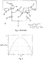
- FIG. 1 illustrates a conventional hysteretic buck converter 10.
- a power source 12 providing an input voltage V in is selectively connected to an inductor 14 by a switching element 16 in the form of a MOSFET.
- a power output 18 is coupled to the inductor 14 for providing an output voltage V out to a load (not shown).
- a diode 20 is connected in parallel with the power source 12 and switching element 16.
- a capacitor 22 is connected in parallel with the power output 18 to filter the output voltage V out .
- a resistor 24 is provided in series with the inductor 14 for sensing the current through the inductor 14.
- a current comparator 26 with hysteresis compares the sensed inductor current with upper and lower reference values and outputs a control signal V CMP for controlling the switching element 16 via a gate drive 28.
- the switching element 16 When the switching element 16 is on, the current I L through the inductor 14 rises at a rate (V in - V out )/L, where L is the inductance of the inductor 14, until it reaches the upper reference value of the current comparator 26.
- the control signal V CMP output by the current comparator 26 then transitions to low, and the switching element 16 is commanded to switch off via the gate drive 28.
- the switching element 16 is off, the inductor current falls at a rate V out /L until it reaches the lower reference value of the current comparator 26.
- the control signal V CMP output by the current comparator 26 then transitions to high, causing the switching element 16 to switch on.
- T on L ⁇ I pp / V in ⁇ V out
- T off L ⁇ I pp / V out
- I pp is the peak-to-peak inductor current ripple
- the conventional hysteretic converter 10 has a fixed current ripple I pp , which is determined by the magnitude of the hysteresis of the current comparator 26.
- This variable frequency is often unwanted, since it can cause audible noise and may be hard to filter.
- the output voltage V out changes frequently with the number of shorted LEDs.
- the switching frequency f will therefore also vary frequently and over a wide range. This makes filtering more complicated and expensive.
- a switch-mode power converter comprising:
- the frequency of the power converter may be stabilized while retaining the fast and stable response of a hysteretic converter. Frequency stabilization may therefore be achieved without using a clock signal.
- the control signal may cause the switching device to have an on-time proportional to V out / V in , and an off-time proportional to 1-V out / V in .
- the switching frequency of the power converter may be independent of duty cycle.
- the current comparator may have no hysteresis.
- the reference current level may correspond to an average current level, in particular when the power converter is in steady state operation.
- the current comparator output signal has a 50% duty cycle when the switch-mode power converter is in steady-state operation.
- the reference current level may be constant.
- the first/second voltage ramp may be triggered by the current comparator output signal.
- the slope of said first/second voltage ramp may be proportional to V in .
- the first/second voltage ramp may be generated by charging a capacitor from a current source.
- the current source may be provided by at least one of the following:
- the first reference voltage may be proportional to (V in -V ou t).
- the second reference voltage may be proportional to V out .
- the first and/or second reference voltage may be provided by at least one of the following:
- the switch-mode power converter may comprise further circuitry for varying one of said first and second time delays to compensate delays in the power converter.
- Said further circuitry may be configured to inject additional current into the control circuit to increase one of the reference voltages and thereby increase the respective time delay. Said further circuitry may be configured to inject additional current into the control circuit when the output signal of the current comparator has a duty cycle not equal to 50%.
- the additional current may be generated by integrating a net current obtained from a first current source having a fixed value and an opposing second current source controlled by the output signal of the current comparator.
- the first / second time delay may be generated using a digital counter.
- the input and/or output voltage may be measured using an analog-to-digital converter.
- a power supply for an LED matrix comprising a switch-mode power converter as defined above.
- This may be useful for providing a constant current output to the LED matrix with a switching frequency substantially independent of output voltage.
- the conventional hysteretic converter 10 shown in Figure 1 exhibits a switching frequency f which varies with output voltage V out .
- the present invention is based on the realisation that the switching frequency may be stabilised by making the hysteresis, and thus the current ripple I pp , dependent on the output voltage V out .
- the current ripple I pp approaches zero, which is acceptable.
- the invention is implemented based on a hysteretic converter with emulated current ripple, also called a median converter because the median of the current is kept constant.
- This converter uses two counters or sawtooth generators to emulate the ripple current.
- a benefit of the median converter is its lower sensitivity to delays in the power stage.
- FIG. 3 shows a median converter 110 with fixed current ripple I pp , useful for understanding the present invention.
- a power source 12 providing an input voltage V in is selectively connected to an inductor 14 by a switching element 16 in the form of a MOSFET.
- a power output 18 is coupled to the inductor 14 for providing an output voltage V out to a load 30 in the form of an LED.
- a diode 20 is connected in parallel with the power source 12 and switching element 16.
- a capacitor 22 is connected in parallel with the power output 18 to filter the output voltage V out .
- a resistor 24 is provided in series with the inductor 14 for sensing the current through the inductor 14.
- a current comparator 126 with no hysteresis compares the sensed inductor current I L with a reference value I REF and outputs a current comparator output signal V CMP .
- the current comparator 126 has no hysteresis.
- a control circuit 140 receives the current comparator output signal V CMP and generates a control signal V Ctrl ' for controlling the switching element 16 via a gate drive 128.
- the current comparator 126 of the median converter 110 toggles at the average current, which is exactly halfway up each slope.
- the current comparator output signal V CMP will have a 50 % duty-cycle.
- the control circuit 140 is therefore required to convert the current comparator output signal V CMP into a control signal V Ctrl suitable for controlling the switching element 16 via the gate drive 128 at the correct timing, i.e. at times at which the inductor current reaches the desired maximum and minimum values.
- the control circuit 140 receives the output V CMP of the current comparator 126, generates first and second time delays ⁇ t 1 ' and ⁇ t 2 ' using sawtooth generators and outputs the control signal V Ctrl ' based on the current comparator output signal V CMP and the first and second time delays. As shown in Figure 4 , the transitions of the control signal V Ctrl ' used for switching the switching element 16 on and off are delayed relative to the transitions of the current comparator output signal V CMP by the first and second time delays ⁇ t 1 ' and ⁇ t 2 'respectively.
- the first time delay ⁇ t 1 ' is generated by comparing a voltage ramp V ramp1 ' having slope V out and a reference voltage V ref1 ' set at a fixed value, for example 1V.
- a current source 152 providing a current proportional to V out , is connected to a capacitor 154, which is selectively shorted to ground by a switch 156.
- the switch 156 is controlled by a signal output from an inverter 157 which inverts the output signal V CMP from the current comparator 126.
- the output voltage V CMP of the current comparator 126 transitions to low when the inductor current I L decreases below the reference value I REF , and the output of the inverter 157 correspondingly transitions high, causing switch 156 to open and the capacitor 154 to start charging from the current source 152.
- the voltage V ramp1 ' across the capacitor 154 increases at a rate proportional to the current output by current source 152, i.e. at a rate proportional to V out .
- a first voltage comparator 158 compares V ramp1 ' with the fixed reference voltage V ref1 ' and its output transitions high when V ramp1 ' increases above V ref1 '. This occurs at a time ⁇ t 1 ', proportional to 1/ V out , after the output V CMP of the current comparator 126 transitions to low.
- the second time delay ⁇ t 2 ' proportional to 1/ (V in -V out ), is generated by comparing a voltage ramp V ramp2 ' having slope V in -V out and a reference voltage V ref2 ' set at a fixed value, for example 1V.
- a current source 162 providing a current proportional to V in -V out , is connected to a capacitor 164, which is selectively shorted to ground by a switch 166.
- the switch 166 is controlled by the output signal V CMP from the current comparator 126.
- the output voltage V CMP of the current comparator 126 transitions to high when the inductor current I L increase above the reference value I REF , causing switch 166 to open and the capacitor 164 to start charging from the current source 162.
- the voltage V ramp2 ' across the capacitor 164 increases at a rate proportional to the current output by current source 162, i.e. at a rate proportional to V in -V out .
- a second voltage comparator 168 compares V ramp2 ' with the fixed reference voltage V ref2 ' and its output transitions high when V ramp2 ' increases above V ref2 '. This occurs at a time ⁇ t 2 ', proportional to 1/ (V in -Vout), after the output V CMP of the current comparator 126 transitions to high.
- the outputs of the first and second voltage comparators 158, 168 are connected to the set and reset inputs respectively of a latch 170.
- the output V ctrl ' of the latch 170 is used to control the switching element 16 via gate drive 128. Since the slope of each analog delay sawtooth ramp V ramp1 ' and V ramp2 ' is related to the input and output voltages V in and V out in the same way as the inductor ripple current, the use of constant reference voltages V ref1 ' and V ref2 ' results in a fixed current ripple I pp or hysteresis, as can be seen in Figure 4 . However, as discussed above, a constant current ripple I pp results in a variable frequency f.
- FIG. 5 shows a converter 210 with variable ripple current I pp (V in , V out ), according to an embodiment of the present invention.
- a power source 12 providing an input voltage V in is selectively connected to an inductor 14 by a switching element 16 in the form of a MOSFET.
- a power output 18 is coupled to the inductor 14 for providing an output voltage V out to a load 30 in the form of an LED.
- a diode 20 is connected in parallel with the power source 12 and switching element 16.
- a capacitor 22 is connected in parallel with the power output 18 to filter the output voltage V out .
- a resistor 24 is provided in series with the inductor 14 for sensing the current through the inductor 14.
- a current comparator 126 with no hysteresis compares the sensed inductor current I L with a reference value I REF and outputs a current comparator output signal V CMP .
- the current comparator 126 has no hysteresis.
- a control circuit 240 receives the current comparator output signal V CMP and generates a control signal Vctri for controlling the switching element 16 via a gate drive 128.
- the control circuit 240 receives the output V CMP of the current comparator 126, generates first and second time delays ⁇ t 1 and ⁇ t 2 using sawtooth generators and outputs a control signal V Ctrl based on the current comparator output signal V CMP and the first and second time delays.
- the transitions of the control signal V Ctrl used for switching the switching element 16 on and off are delayed relative to the transitions of the current comparator output signal V CMP by the first and second time delays ⁇ t 1 and ⁇ t 2 respectively.
- the control circuit 240 in this embodiment differs from the control circuit 140 of the median converter 110 shown in Figure 3 in that it generates first and second time delays ⁇ t 1 and ⁇ t 2 which depend on the input and output voltages V in and V out in such a way as to reduce or eliminate variations in the switching frequency of the converter 240. As a result, the ripple current Ipp is not fixed.
- Ipp V in V out 1 f ⁇ L ⁇ V out ⁇ V in ⁇ V out
- the control circuit 240 generates a first time delay ⁇ t 1 proportional to V out / V in and a second time delay ⁇ t 2 proportional to (V in - V out ) / V in .
- each time delay is inversely proportional to the capacitor charging current and proportional to the voltage comparator reference level.
- the capacitor charging current is proportional to 1/V in for both delay times, while the voltage comparator levels are proportional to V out and (V in -V out ) respectively.
- the first time delay ⁇ t 1 proportional to V out /V in , is generated by comparing a voltage ramp V ramp1 having slope proportional to V in and a reference voltage V ref1 proportional to V out .
- a current source 252 providing a current proportional to V in , is connected to a capacitor 254, which is selectively shorted to ground by a switch 256.
- the switch 256 is controlled by a signal output from an inverter 257 which inverts the output signal V CMP from the current comparator 126.
- the output voltage V CMP of the current comparator 126 transitions to low when the inductor current I L decreases below the reference value I REF , and the output of the inverter 257 correspondingly transitions high, causing switch 256 to open and the capacitor 254 to start charging from the current source 252.
- the voltage V ramp1 across the capacitor 254 increases at a rate proportional to the current output by current source 252, i.e. at a rate proportional to V in .
- a first voltage comparator 258 compares V ramp1 with the reference voltage V ref1 proportional to V out and its output transitions high when V ramp1 increases above V ref1 . This occurs at a time ⁇ t 1 , proportional to V out /V in , after the output V CMP of the current comparator 126 transitions to low.
- the second time delay ⁇ t 2 proportional to (V in - V out ) / V in , is generated by comparing a voltage ramp V ramp2 having slope V in and a reference voltage V ref2 proportional to (V in - V out ).
- a current source 262 providing a current proportional to V in , is connected to a capacitor 264, which is selectively shorted to ground by a switch 266.
- the switch 266 is controlled by the output signal V CMP from the current comparator 126.
- the output voltage V CMP of the current comparator 126 transitions to high when the inductor current I L increase above the reference value I REF , causing switch 266 to open and the capacitor 264 to start charging from the current source 262.
- V ramp2 across the capacitor 264 increases at a rate proportional to the current output by current source 262, i.e. at a rate proportional to V in .
- a second voltage comparator 268 compares V ramp2 with the reference voltage V ref2 proportional to (V in - V out ) and its output transitions high when V ramp2 increases above V ref2 . This occurs at a time ⁇ t 2 , proportional to (V in - V out ) / V in , after the output V CMP of the current comparator 126 transitions to high.
- the outputs of the first and second voltage comparators 258, 268 are connected to the set and reset inputs respectively of a latch 270.
- the output V ctrl of the latch 270 is used to control the switching element 16 via gate drive 128.
- the current ripple I pp now varies with output voltage V out , but the switching frequency f remains substantially constant.
- the current sources 252, 262 proportional to V in used to generate the voltage ramps V ramp1 and V ramp2 input to the first and second voltage comparators 258, 268, may be implemented in various ways, including using a simple resistor ( Figure 6A ), current mirrors ( Figure 6B ), cascoded mirror ( Figures 6C ) or a cascoded mirror with offset compensation ( Figure 6D ).
- a current proportional to V in is generated at the output indicated by the arrow.
- the basic current mirror shown in Figure 6B converts the input supply voltage V in to a proportional current.
- Such a circuit is known to have a moderate output impedance due to the Early effect.
- the output current will be influenced by the voltage on the output terminal.
- the cascoded mirror shown in Figure 6C has a much better output impedance. However, there is an error in the conversion of voltage to current due to the two gate threshold voltages of the MOSFETS Q2, Q4 in series with the resistor R5. The missing current is 2*(threshold voltage)/R5. Especially for low V in , the current will be lower than desired.
- the cascoded mirror with offset compensation shown in Figure 6D includes an additional op amp U2 and transistor Q5 which generates the required extra current.
- the reference levels V ref1 and V ref2 input to the first and second voltage comparators 258, 268 can also be implemented using current mirror arrangements similar to those used for the current sources 252, 262.
- Figures 7A and 7B show cascoded mirrors with offset compensation for generating V ref1 and V ref2 respectively.
- the voltage V ref1 generated across resistive element R7 is proportional to (V in - V out ).
- the voltage V ref2 generated across resistive element R7 is proportional to V out .
- This circuit may be replaced by a resistive voltage divider for generating V ref2 .
- Figure 8 shows results of a simulation of the median converter with fixed current ripple as described above with reference to Figure 3 .
- the output voltage V out increases from about 7.8V to about 11.8V.
- the inductor current I L has a fixed current ripple I pp , but the frequency of the current ripple varies with output voltage V out .
- the output voltage V out increases from about 7.8V to about 11.8V.
- the inductor current I L now has a current ripple I pp of variable magnitude.
- the frequency of the current ripple is substantially fixed at about 500kHz.
- the output voltage V out has a negative slope at 310 ⁇ s, decreasing from about 11.8V to 7.8 V. Again, the frequency of the converter is fixed.
- the power converter of the present invention may include further circuitry for varying one of the first or second time delays ⁇ t 1 , ⁇ t 2 to compensate such delays.
- Figure 11 shows circuitry for generating the current sources 252 and 262 and the reference voltages V ref1 and V ref2 ., and includes further circuitry, in the form of a simple control circuit 280, which can inject some extra current into one of the delay circuits to raise the trigger level V ref1 or V ref2 and make the respective time delay ⁇ t 1 , ⁇ t 2 longer.
- the current sources 252 and 262 are proportional to V in and are implemented using simple resistors R16 and R8.
- the second reference voltage V ref2 proportional to V out , is obtained by a resistive divider.
- the first reference voltage V ref1 proportional to V in -V out , is obtained by a cascoded current mirror with offset compensation (similar to the arrangement shown in Figure 6D ) with further compensation provided by the additional control circuit shown in the dashed rectangle.
- the additional control circuit 280 includes one fixed current source CS1 (in this example, 5 ⁇ A) and one switched current source CS2 (in this example, 0, 10 ⁇ A), controlled by the output voltage V CMP of the current comparator 126, which should have a 50% duty cycle.
- the fixed current source and switched current source of the control circuit deliver zero net current.
- the resulting net current is integrated and the filter voltage output by the control circuit is used to drive a current source that adds to the normal current source.
- a Sample & Hold circuit filters out the switching frequency ripple. The extra current can make the off-time T off longer, by increasing V ref1 .
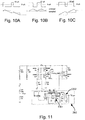
- FIGS 10A-C The effect of the control circuit 280 of Figure 11 is illustrated in Figures 10A-C .
- the current is too low.
- the duty cycle of the current comparator 126 is less than 50%, and the current sampled by the control current decreases, resulting in reduction of V ref1 and a shortening of T off .
- the current is correct.
- the duty cycle of the current comparator 126 is exactly 50%, and the sampled current in the control circuit is zero, so that the control circuit makes no change to V ref1 .
- FIG 10C the current is too high.
- the duty cycle of the current comparator 126 is greater than 50%, and the current sampled by the control current increases, resulting in an increase of V ref1 and a lengthening of T off .
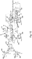
- FIG. 12 A further embodiment of a power converter according to the present invention is shown in Figure 12 , for integration with the circuitry of Figure 11 .
- the diode 20 of the embodiment shown in Figure 5 is replaced by a further switching element 16B.
- the converter is always in Continuous Conduction mode, and the frequency remains close to a constant value
- the converter can enter Discontinuous Current Mode, in which the equations given above no longer apply and the frequency becomes lower. Nonetheless, even in Discontinuous Current Mode, the frequency of this design remains between 250 kHz and 600 kHz, which is a lot better than the conventional hysteretic converter.
- the adjustment of the current ripple is done by means of feed-forward to improve speed and maintain stability. It is an open-loop addition that does not influence stability.
- the invention may be based on a modified median converter with no external components required. All components may be so small they can be integrated, and their values are not critical.
- An extra feedback loop as described above in connection with Figure 11 may reduce the effect of delays in the power stages and current comparator for best current accuracy.
Landscapes
- Engineering & Computer Science (AREA)
- Power Engineering (AREA)
- Dc-Dc Converters (AREA)
Abstract
A switch-mode power converter (210) is described, the switch-mode power converter (210) comprising: an inductive element (14) having an input and an output; a switching device (16) for selectively connecting said input of said inductive element (14) to a power source (12); a power output (18) for connection to a load (30), said power output (180) being coupled to said output of said inductive element (14); a current comparator (126) configured to generate a current comparator output signal (V CMP ) based on a comparison of a current flowing through the inductive element (14) and a reference current level (I REF ); and a control circuit (240) for generating a control signal (V Ctrl ) for controlling the switching device (16), wherein the control circuit (240) is configured to generate said control signal (V Ctrl ) based on the current comparator output signal (V CMP ), a first time delay (t 1 ) proportional to (V in - V out ) / V in and a second time delay (t 2 ) proportional to V out / Vin where Vin is the voltage at the power source (12) and V out is the voltage at the power output (18).
Description
- The present invention relates to a switch-mode power converter and to an LED power supply including the switch-mode power converter. In particular, but not exclusively, the invention relates to a switch-mode power converter with feed-forward dependent on input and output voltage for reducing or eliminating variations in switching frequency.
-
Figure 1 illustrates a conventionalhysteretic buck converter 10. Apower source 12 providing an input voltage Vin is selectively connected to aninductor 14 by aswitching element 16 in the form of a MOSFET. Apower output 18 is coupled to theinductor 14 for providing an output voltage Vout to a load (not shown). Adiode 20 is connected in parallel with thepower source 12 and switchingelement 16. Acapacitor 22 is connected in parallel with thepower output 18 to filter the output voltage Vout. A resistor 24 is provided in series with theinductor 14 for sensing the current through theinductor 14. Acurrent comparator 26 with hysteresis compares the sensed inductor current with upper and lower reference values and outputs a control signal VCMP for controlling theswitching element 16 via agate drive 28. - When the
switching element 16 is on, the current IL through theinductor 14 rises at a rate (Vin - Vout)/L, where L is the inductance of theinductor 14, until it reaches the upper reference value of thecurrent comparator 26. The control signal VCMP output by thecurrent comparator 26 then transitions to low, and theswitching element 16 is commanded to switch off via thegate drive 28. When theswitching element 16 is off, the inductor current falls at a rate Vout/L until it reaches the lower reference value of thecurrent comparator 26. The control signal VCMP output by thecurrent comparator 26 then transitions to high, causing theswitching element 16 to switch on. The on-time Ton (and thus the duration of the rising slope of the current) and off-time Toff (and thus the duration of the falling slope of the current) of thepower converter 10 are given by:

- The conventional
hysteretic converter 10 has a fixed current ripple Ipp, which is determined by the magnitude of the hysteresis of thecurrent comparator 26. As a result, the switching frequency f of the conventionalhysteretic converter 10 depends on the magnitude of the hysteresis Ipp, the input voltage Vin, the output voltage Vout and the inductor value L:
- In the case of a variable output voltage Vout, the switching frequency f shows a parabolic dependence on Vout and varies between zero (at Vout = 0 and Vout = Vin) and a maximum at 50 % duty-cycle (i.e. for Vout / Vin = 0.5). This variable frequency is often unwanted, since it can cause audible noise and may be hard to filter.
- In LED matrix applications, the output voltage Vout changes frequently with the number of shorted LEDs. The switching frequency f will therefore also vary frequently and over a wide range. This makes filtering more complicated and expensive.
- Aspects of the invention are set out in the accompanying claims. Combinations of features from the dependent claims may be combined with features of the independent claims as appropriate and not merely as explicitly set out in the claims.
- According to an aspect of the invention, there is provided a switch-mode power converter comprising:
- an inductive element having an input and an output;
- a switching device for selectively connecting said input of said inductive element to a power source;
- a power output for connection to a load, said power output being coupled to said output of said inductive element;
- a current comparator configured to generate a current comparator output signal based on a comparison of a current flowing through the inductive element and a reference current level; and
- a control circuit for generating a control signal for controlling the switching device, wherein the control circuit is configured to generate said control signal based on the current comparator output signal, a first time delay proportional to (Vin - Vout) / Vin and a second time delay proportional to Vout / Vin where Vin is the voltage at the power source and Vout is the voltage at the power output.
- By making the first time delay proportional to (Vin - Vout) / Vin and the second time delay proportional to Vout / Vin, where Vin is the voltage at the power source and Vout is the voltage at the power output, the frequency of the power converter may be stabilized while retaining the fast and stable response of a hysteretic converter. Frequency stabilization may therefore be achieved without using a clock signal.
- The control signal may cause the switching device to have an on-time proportional to Vout / Vin, and an off-time proportional to 1-Vout / Vin.
- As a result, the switching frequency of the power converter may be independent of duty cycle.
- The current comparator may have no hysteresis.
- The reference current level may correspond to an average current level, in particular when the power converter is in steady state operation.
- In some embodiments of the invention, the current comparator output signal has a 50% duty cycle when the switch-mode power converter is in steady-state operation.
- The reference current level may be constant.
- By holding the reference current level constant, a constant output current is provided during operation with a load connected to the power output.
- In some embodiments of the power converter:
- said control signal commands said switching device to switch on at a time equal to said first time delay after said current comparator output signal indicates that said current decreases to a level below said reference current level, and
- said control signal commands said switching device to switch off at a time equal to said second time delay after said current comparator output signal indicates said current increases to a level above said reference current level.
- In some embodiments of the power converter:
- said first time delay is implemented using a first voltage ramp and a first voltage comparator for comparing said first voltage ramp with a first reference voltage, and/or
- said second time delay is implemented using a second voltage ramp and a second voltage comparator for comparing said second voltage ramp with a second reference voltage.
- The first/second voltage ramp may be triggered by the current comparator output signal.
- The slope of said first/second voltage ramp may be proportional to Vin.
- The first/second voltage ramp may be generated by charging a capacitor from a current source.
- The current source may be provided by at least one of the following:
- a resistance;
- a current mirror;
- a cascoded current mirror; and/or
- a cascoded current mirror with offset compensation.
- The first reference voltage may be proportional to (Vin-Vout).
- The second reference voltage may be proportional to Vout.
- The first and/or second reference voltage may be provided by at least one of the following:
- a voltage divider;
- a current mirror;
- a cascoded mirror; or
- a cascoded mirror with offset compensation.
- The switch-mode power converter may comprise further circuitry for varying one of said first and second time delays to compensate delays in the power converter.
- This may be particularly useful when operating the power converter at very low current, in which case delays in the power stage may result in an error in the current and a current comparator output signal which deviates from a 50% duty cycle. Said further circuitry may be configured to inject additional current into the control circuit to increase one of the reference voltages and thereby increase the respective time delay. Said further circuitry may be configured to inject additional current into the control circuit when the output signal of the current comparator has a duty cycle not equal to 50%. The additional current may be generated by integrating a net current obtained from a first current source having a fixed value and an opposing second current source controlled by the output signal of the current comparator.
- In some embodiments, the first / second time delay may be generated using a digital counter.
- The input and/or output voltage may be measured using an analog-to-digital converter.
- According to a further aspect of the invention, there is provided a power supply for an LED matrix, comprising a switch-mode power converter as defined above.
- This may be useful for providing a constant current output to the LED matrix with a switching frequency substantially independent of output voltage.
- Embodiments of the present invention will be described, by way of example only, with reference to the accompanying drawings in which like reference signs relate to like elements and in which:
-
Figure 1 shows a conventional hysteretic buck converter useful for understanding the present invention; -
Figure 2 illustrates the required current ripple Ipp as a function of duty cycle δ=Vout/Vin for maintaining a substantially constant switching frequency; -
Figure 3 illustrates a median converter with fixed current ripple useful for understanding the present invention; -
Figure 4 illustrates the variation with time of control voltage VCtrl, inductor current IL, current comparator output signal VCMP, and first and second voltage ramps Vramp1 and Vramp2 in the median converter with fixed current ripple ofFigure 3 ; -
Figure 5 illustrates a power converter according to an embodiment of the present invention; -
Figures 6A to 6D illustrate various implementations of thecurrent sources Figure 5 ; -
Figures 7A and 7B show cascoded current mirrors with offset compensation for generating reference voltages proportional to Vin-Vout and Vout respectively for thevoltage comparators Figure 5 ; -
Figure 8 shows the results of a simulation of the median converter with fixed current ripple shown inFigure 3 ; -
Figures 9A-C show the results of simulations of the power converter with variable current ripple shown inFigure 5 ; -
Figures 10A-C illustrate the effect of thecontrol circuit 280 shown inFigure 11 ; -
Figure 11 shows circuitry for generating thecurrent sources voltage comparators Figure 5 ; and -
Figure 12 shows a power converter according to a further embodiment of the present invention. - As discussed above, the conventional
hysteretic converter 10 shown inFigure 1 exhibits a switching frequency f which varies with output voltage Vout. The present invention is based on the realisation that the switching frequency may be stabilised by making the hysteresis, and thus the current ripple Ipp, dependent on the output voltage Vout. - For the switching frequency


- By making the current ripple Ipp dependent on output voltage Vout and duty-cycle δ = Vout/Vin, the switching frequency f becomes constant.
-
Figure 2 shows the required variation of the current ripple Ipp (Vin, Vout) as a function of duty-cycle δ = Vout/Vin, for f = 500 kHz, Vin = 60 V and L = 68 µH. For low and high duty-cycles, the current ripple Ipp approaches zero, which is acceptable. - The invention is implemented based on a hysteretic converter with emulated current ripple, also called a median converter because the median of the current is kept constant. This converter uses two counters or sawtooth generators to emulate the ripple current. A benefit of the median converter is its lower sensitivity to delays in the power stage.
-
Figure 3 shows amedian converter 110 with fixed current ripple Ipp, useful for understanding the present invention. Apower source 12 providing an input voltage Vin is selectively connected to aninductor 14 by a switchingelement 16 in the form of a MOSFET. Apower output 18 is coupled to theinductor 14 for providing an output voltage Vout to aload 30 in the form of an LED. Adiode 20 is connected in parallel with thepower source 12 and switchingelement 16. Acapacitor 22 is connected in parallel with thepower output 18 to filter the output voltage Vout. A resistor 24 is provided in series with theinductor 14 for sensing the current through theinductor 14. Acurrent comparator 126 with no hysteresis compares the sensed inductor current IL with a reference value IREF and outputs a current comparator output signal VCMP. In themedian converter 110, thecurrent comparator 126 has no hysteresis. A control circuit 140 receives the current comparator output signal VCMP and generates a control signal VCtrl' for controlling the switchingelement 16 via agate drive 128. - Assuming the inductor current IL increases and decreases linearly with time, the
current comparator 126 of themedian converter 110 toggles at the average current, which is exactly halfway up each slope. When operating in steady state with the average inductor current at a value corresponding to the setpoint or reference current level IREF of thecurrent comparator 126, the current comparator output signal VCMP will have a 50 % duty-cycle. The control circuit 140 is therefore required to convert the current comparator output signal VCMP into a control signal VCtrl suitable for controlling the switchingelement 16 via thegate drive 128 at the correct timing, i.e. at times at which the inductor current reaches the desired maximum and minimum values. - The control circuit 140 receives the output VCMP of the
current comparator 126, generates first and second time delays Δt1' and Δt2' using sawtooth generators and outputs the control signal VCtrl' based on the current comparator output signal VCMP and the first and second time delays. As shown inFigure 4 , the transitions of the control signal VCtrl' used for switching the switchingelement 16 on and off are delayed relative to the transitions of the current comparator output signal VCMP by the first and second time delays Δt1' and Δt2'respectively. To emulate the fixed current ripple Ipp of the conventional hysteretic converter shown inFigure 1 , the median converter with fixed current ripple shown inFigure 3 generates a first time delay Δt1' proportional to Toff = L · Ipp / (Vout) and a second time delay Δt2'proportional to Ton = L · Ipp / (Vin-Vout) respectively, where Ipp is the required fixed current ripple. - The first time delay Δt1', proportional to 1/ Vout , is generated by comparing a voltage ramp Vramp1' having slope Vout and a reference voltage Vref1' set at a fixed value, for example 1V. A
current source 152, providing a current proportional to Vout, is connected to acapacitor 154, which is selectively shorted to ground by aswitch 156. Theswitch 156 is controlled by a signal output from aninverter 157 which inverts the output signal VCMP from thecurrent comparator 126. During the off time of the switchingelement 16, the output voltage VCMP of thecurrent comparator 126 transitions to low when the inductor current IL decreases below the reference value IREF, and the output of theinverter 157 correspondingly transitions high, causingswitch 156 to open and thecapacitor 154 to start charging from thecurrent source 152. The voltage Vramp1' across thecapacitor 154 increases at a rate proportional to the current output bycurrent source 152, i.e. at a rate proportional to Vout. Afirst voltage comparator 158 compares Vramp1' with the fixed reference voltage Vref1' and its output transitions high when Vramp1' increases above Vref1'. This occurs at a time Δt1', proportional to 1/ Vout, after the output VCMP of thecurrent comparator 126 transitions to low. - The second time delay Δt2', proportional to 1/ (Vin-Vout), is generated by comparing a voltage ramp Vramp2' having slope Vin-Vout and a reference voltage Vref2' set at a fixed value, for example 1V. A
current source 162, providing a current proportional to Vin-Vout, is connected to acapacitor 164, which is selectively shorted to ground by aswitch 166. Theswitch 166 is controlled by the output signal VCMP from thecurrent comparator 126. During the on time of the switchingelement 16, the output voltage VCMP of thecurrent comparator 126 transitions to high when the inductor current IL increase above the reference value IREF, causingswitch 166 to open and thecapacitor 164 to start charging from thecurrent source 162. The voltage Vramp2' across thecapacitor 164 increases at a rate proportional to the current output bycurrent source 162, i.e. at a rate proportional to Vin-Vout. Asecond voltage comparator 168 compares Vramp2' with the fixed reference voltage Vref2' and its output transitions high when Vramp2' increases above Vref2'. This occurs at a time Δt2', proportional to 1/ (Vin-Vout), after the output VCMP of thecurrent comparator 126 transitions to high. - The outputs of the first and
second voltage comparators latch 170. The output Vctrl' of thelatch 170 is used to control the switchingelement 16 viagate drive 128. Since the slope of each analog delay sawtooth ramp Vramp1' and Vramp2' is related to the input and output voltages Vin and Vout in the same way as the inductor ripple current, the use of constant reference voltages Vref1' and Vref2' results in a fixed current ripple Ipp or hysteresis, as can be seen inFigure 4 . However, as discussed above, a constant current ripple Ipp results in a variable frequency f. -
Figure 5 shows aconverter 210 with variable ripple current Ipp(Vin, Vout), according to an embodiment of the present invention. Apower source 12 providing an input voltage Vin is selectively connected to aninductor 14 by a switchingelement 16 in the form of a MOSFET. Apower output 18 is coupled to theinductor 14 for providing an output voltage Vout to aload 30 in the form of an LED. Adiode 20 is connected in parallel with thepower source 12 and switchingelement 16. Acapacitor 22 is connected in parallel with thepower output 18 to filter the output voltage Vout. A resistor 24 is provided in series with theinductor 14 for sensing the current through theinductor 14. Acurrent comparator 126 with no hysteresis compares the sensed inductor current IL with a reference value IREF and outputs a current comparator output signal VCMP. Thecurrent comparator 126 has no hysteresis. - A
control circuit 240 receives the current comparator output signal VCMP and generates a control signal Vctri for controlling the switchingelement 16 via agate drive 128. Thecontrol circuit 240 receives the output VCMP of thecurrent comparator 126, generates first and second time delays Δt1 and Δt2 using sawtooth generators and outputs a control signal VCtrl based on the current comparator output signal VCMP and the first and second time delays. The transitions of the control signal VCtrl used for switching the switchingelement 16 on and off are delayed relative to the transitions of the current comparator output signal VCMP by the first and second time delays Δt1 and Δt2 respectively. Thecontrol circuit 240 in this embodiment differs from the control circuit 140 of themedian converter 110 shown inFigure 3 in that it generates first and second time delays Δt1 and Δt2 which depend on the input and output voltages Vin and Vout in such a way as to reduce or eliminate variations in the switching frequency of theconverter 240. As a result, the ripple current Ipp is not fixed. - As discussed above, for the switching frequency f to be constant, the current ripple Ipp must vary with Vin and Vout as follows:

- Thus the on time Ton is given by:


converter 210 and f is a constant switching frequency. - The
control circuit 240 generates a first time delay Δt1 proportional to Vout / Vin and a second time delay Δt2 proportional to (Vin - Vout) / Vin. - Using sawtooth generators to generate the time delays, each time delay is inversely proportional to the capacitor charging current and proportional to the voltage comparator reference level. In this embodiment, the capacitor charging current is proportional to 1/Vin for both delay times, while the voltage comparator levels are proportional to Vout and (Vin-Vout) respectively.
- The first time delay Δt1, proportional to Vout /Vin, is generated by comparing a voltage ramp Vramp1 having slope proportional to Vin and a reference voltage Vref1 proportional to Vout. A
current source 252, providing a current proportional to Vin, is connected to acapacitor 254, which is selectively shorted to ground by aswitch 256. Theswitch 256 is controlled by a signal output from aninverter 257 which inverts the output signal VCMP from thecurrent comparator 126. During the off time of the switchingelement 16, the output voltage VCMP of thecurrent comparator 126 transitions to low when the inductor current IL decreases below the reference value IREF, and the output of theinverter 257 correspondingly transitions high, causingswitch 256 to open and thecapacitor 254 to start charging from thecurrent source 252. The voltage Vramp1 across thecapacitor 254 increases at a rate proportional to the current output bycurrent source 252, i.e. at a rate proportional to Vin. Afirst voltage comparator 258 compares Vramp1 with the reference voltage Vref1 proportional to Vout and its output transitions high when Vramp1 increases above Vref1. This occurs at a time Δt1, proportional to Vout/Vin, after the output VCMP of thecurrent comparator 126 transitions to low. - The second time delay Δt2, proportional to (Vin - Vout) / Vin, is generated by comparing a voltage ramp Vramp2 having slope Vin and a reference voltage Vref2 proportional to (Vin - Vout). A
current source 262, providing a current proportional to Vin, is connected to acapacitor 264, which is selectively shorted to ground by aswitch 266. Theswitch 266 is controlled by the output signal VCMP from thecurrent comparator 126. During the on time of the switchingelement 16, the output voltage VCMP of thecurrent comparator 126 transitions to high when the inductor current IL increase above the reference value IREF, causingswitch 266 to open and thecapacitor 264 to start charging from thecurrent source 262. The voltage Vramp2 across thecapacitor 264 increases at a rate proportional to the current output bycurrent source 262, i.e. at a rate proportional to Vin. Asecond voltage comparator 268 compares Vramp2 with the reference voltage Vref2 proportional to (Vin - Vout) and its output transitions high when Vramp2 increases above Vref2. This occurs at a time Δt2, proportional to (Vin - Vout) / Vin, after the output VCMP of thecurrent comparator 126 transitions to high. - The outputs of the first and
second voltage comparators latch 270. The output Vctrl of thelatch 270 is used to control the switchingelement 16 viagate drive 128. The current ripple Ipp now varies with output voltage Vout, but the switching frequency f remains substantially constant. - The
current sources second voltage comparators Figure 6A ), current mirrors (Figure 6B ), cascoded mirror (Figures 6C ) or a cascoded mirror with offset compensation (Figure 6D ). In each of the circuits shown inFigures 6A to 6D , a current proportional to Vin is generated at the output indicated by the arrow. The basic current mirror shown inFigure 6B converts the input supply voltage Vin to a proportional current. Such a circuit is known to have a moderate output impedance due to the Early effect. The output current will be influenced by the voltage on the output terminal. The cascoded mirror shown inFigure 6C has a much better output impedance. However, there is an error in the conversion of voltage to current due to the two gate threshold voltages of the MOSFETS Q2, Q4 in series with the resistor R5. The missing current is 2*(threshold voltage)/R5. Especially for low Vin, the current will be lower than desired. The cascoded mirror with offset compensation shown inFigure 6D includes an additional op amp U2 and transistor Q5 which generates the required extra current. - The reference levels Vref1 and Vref2 input to the first and
second voltage comparators current sources Figures 7A and 7B show cascoded mirrors with offset compensation for generating Vref1 and Vref2 respectively. InFigure 7A , the voltage Vref1 generated across resistive element R7 is proportional to (Vin - Vout). InFigure 7B , the voltage Vref2 generated across resistive element R7 is proportional to Vout. This circuit may be replaced by a resistive voltage divider for generating Vref2. These circuits rely on matching and are very suitable for integration. -
Figure 8 shows results of a simulation of the median converter with fixed current ripple as described above with reference toFigure 3 . At time 310µs, the output voltage Vout increases from about 7.8V to about 11.8V. The inductor current IL has a fixed current ripple Ipp, but the frequency of the current ripple varies with output voltage Vout. -
Figure 9A shows the results of a simulation of the converter according to the embodiment of the present invention described above with reference toFigure 5 , with inductance L=47µH and input voltage Vin=60V. As in the previous example, at time 310µs, the output voltage Vout increases from about 7.8V to about 11.8V. The inductor current IL now has a current ripple Ipp of variable magnitude. However the frequency of the current ripple is substantially fixed at about 500kHz. -
Figure 9B shows the results of another simulation of the converter according to the embodiment of the present invention described above with reference toFigure 5 , with inductance L=47µH and input voltage Vin=25V. The frequency of the current ripple is substantially fixed and is only 5% lower than in the example ofFigure 9A with Vin=60V. -
Figure 9C shows the results of another simulation of the converter according to the embodiment of the present invention described above with reference toFigure 5 , with inductance L=47µH and input voltage Vin=25V. In this example, the output voltage Vout has a negative slope at 310µs, decreasing from about 11.8V to 7.8 V. Again, the frequency of the converter is fixed. - In each of the examples shown in
Figures 9A to 9C , there is a clear change in the amplitude of the current ripple and in the duty-cycle, corresponding to the change in output voltage Vout around time 310µs. However, the frequency remains substantially constant. The median converter (Figure 3 ) already benefits from insensitivity to the inductor value and to delays in the power stage. The present invention retains these advantages, in addition to the further advantage of a constant frequency. Although the frequency is not absolutely fixed, since it is not controlled by an oscillator, it spreads much less than in the case of a conventional hysteretic converter. In the ideal case, the frequency does not vary with input voltage Vin or output voltage Vout. However, small deviations in frequency occur with input voltage Vin and output voltage Vout, for example due to non-linearities in the current sources and leakage of the capacitors, and temperature. Power stage delays introduce a further dependence of the frequency on current. Nonetheless, the variation in frequency is expected to be less than 5-10% when operating in Continuous Current Mode. - For very low currents, delays in the power stage may result in an error in the current and an output VCMP of the current comparator not having a 50 % duty-cycle. The power converter of the present invention may include further circuitry for varying one of the first or second time delays Δt1, Δt2 to compensate such delays.
Figure 11 shows circuitry for generating thecurrent sources simple control circuit 280, which can inject some extra current into one of the delay circuits to raise the trigger level Vref1 or Vref2 and make the respective time delay Δt1, Δt2 longer. In this embodiment, thecurrent sources Figure 6D ) with further compensation provided by the additional control circuit shown in the dashed rectangle. Theadditional control circuit 280 includes one fixed current source CS1 (in this example, 5µA) and one switched current source CS2 (in this example, 0, 10µA), controlled by the output voltage VCMP of thecurrent comparator 126, which should have a 50% duty cycle. When the duty cycle is exactly 50%, the fixed current source and switched current source of the control circuit deliver zero net current. When the duty cycle is not exactly 50%, the resulting net current is integrated and the filter voltage output by the control circuit is used to drive a current source that adds to the normal current source. A Sample & Hold circuit filters out the switching frequency ripple. The extra current can make the off-time Toff longer, by increasing Vref1. - The effect of the
control circuit 280 ofFigure 11 is illustrated inFigures 10A-C . InFigure 10A , the current is too low. The duty cycle of thecurrent comparator 126 is less than 50%, and the current sampled by the control current decreases, resulting in reduction of Vref1 and a shortening of Toff. InFigure 10B , the current is correct. The duty cycle of thecurrent comparator 126 is exactly 50%, and the sampled current in the control circuit is zero, so that the control circuit makes no change to Vref1. InFigure 10C , the current is too high. The duty cycle of thecurrent comparator 126 is greater than 50%, and the current sampled by the control current increases, resulting in an increase of Vref1 and a lengthening of Toff. - A further embodiment of a power converter according to the present invention is shown in
Figure 12 , for integration with the circuitry ofFigure 11 . In this embodiment, thediode 20 of the embodiment shown inFigure 5 is replaced by afurther switching element 16B. In this embodiment, the converter is always in Continuous Conduction mode, and the frequency remains close to a constant value However, it is also possible to rely on a good freewheeling diode. When using a diode instead of a switch, the converter can enter Discontinuous Current Mode, in which the equations given above no longer apply and the frequency becomes lower. Nonetheless, even in Discontinuous Current Mode, the frequency of this design remains between 250 kHz and 600 kHz, which is a lot better than the conventional hysteretic converter. - In the embodiments described above, all circuits are analog. However, it is also possible to implement the invention using digital blocks. The sawtooth generators are then replaced by counters with variable increment. Input and output voltages can be measured with ADCs.
- In the present invention as described above, the adjustment of the current ripple is done by means of feed-forward to improve speed and maintain stability. It is an open-loop addition that does not influence stability. The invention may be based on a modified median converter with no external components required. All components may be so small they can be integrated, and their values are not critical. An extra feedback loop as described above in connection with
Figure 11 may reduce the effect of delays in the power stages and current comparator for best current accuracy. - Although particular embodiments of the invention have been described above, it will be appreciated than many modifications, including additions and/or substitutions, may be made within the scope of the appended claims.
Claims (15)
- A switch-mode power converter comprising:an inductive element having an input and an output;a switching device for selectively connecting said input of said inductive element to a power source;a power output for connection to a load, said power output being coupled to said output of said inductive element,a current comparator configured to generate a current comparator output signal based on a comparison of a current flowing through the inductive element and a reference current level; anda control circuit for generating a control signal for controlling the switching device, wherein the control circuit is configured to generate said control signal based on the current comparator output signal, a first time delay proportional to (Vin - Vout) / Vin and a second time delay proportional to Vout / Vin where Vin is the voltage at the power source and Vout is the voltage at the power output.
- A switch-mode power converter according to claim 1, wherein the control signal causes the switching device to have an on-time proportional to Vout / Vin, and an off-time proportional to 1-Vout / Vin.
- A switch-mode power converter according to claim 1 or claim 2, wherein said reference current level corresponds to an average current level.
- A switch-mode power converter according to any one of the preceding claims, wherein:said control signal commands said switching device to switch on at a time equal to said first time delay after said current comparator output signal indicates that said current decreases to a level below said reference current level, andsaid control signal commands said switching device to switch off at a time equal to said second time delay after said current comparator output signal indicates said current increases to a level above said reference current level.
- A switch-mode power converter according to any one of the preceding claims, wherein:said first time delay is implemented using a first voltage ramp and a first voltage comparator for comparing said first voltage ramp with a first reference voltage, and/orsaid second time delay is implemented using a second voltage ramp and a second voltage comparator for comparing said second voltage ramp with a second reference voltage.
- A switch-mode power converter according to claim 5, wherein said first/second voltage ramp is triggered by the current comparator output signal.
- A switch-mode power converter according to claim 5 or claim 6, wherein a slope of said first/second voltage ramp is proportional to Vin.
- A switch-mode power converter according to any one of claims 5 to 7, wherein said first/second voltage ramp is generated by charging a capacitor from a current source.
- A switch-mode power converter according to claim 8, wherein said current source is provided by at least one of the following:a resistance;a current mirror;a cascoded current mirror; ora cascoded current mirror with offset compensation.
- A switch-mode power converter according to any of claims 5 to 9, wherein said first reference voltage is proportional to (Vin-Vout).
- A switch-mode power converter according to any of claims 5 to 10, wherein said second reference voltage is proportional to Vout.
- A switch-mode power converter according to any of claims 5 to 11, wherein said first and/or second reference voltage is provided by at least one of the following:a voltage divider;a current mirror;a cascoded mirror; ora cascoded mirror with offset compensation.
- A switch-mode power converter according to any of claims 5 to 12, comprising further circuitry for varying one of said first and second time delays to compensate delays in the power converter.
- A switch-mode power converter according to any of claims 1 to 13, wherein said first / second time delay is generated using a digital counter.
- A power supply for an LED matrix, comprising a switch-mode power converter according to any of claims 1 to 14.
Priority Applications (1)
| Application Number | Priority Date | Filing Date | Title |
|---|---|---|---|
| EP17194694.0A EP3468022A1 (en) | 2017-10-04 | 2017-10-04 | Switch-mode power converter |
Applications Claiming Priority (1)
| Application Number | Priority Date | Filing Date | Title |
|---|---|---|---|
| EP17194694.0A EP3468022A1 (en) | 2017-10-04 | 2017-10-04 | Switch-mode power converter |
Publications (1)
| Publication Number | Publication Date |
|---|---|
| EP3468022A1 true EP3468022A1 (en) | 2019-04-10 |
Family
ID=60019784
Family Applications (1)
| Application Number | Title | Priority Date | Filing Date |
|---|---|---|---|
| EP17194694.0A Withdrawn EP3468022A1 (en) | 2017-10-04 | 2017-10-04 | Switch-mode power converter |
Country Status (1)
| Country | Link |
|---|---|
| EP (1) | EP3468022A1 (en) |
Cited By (7)
| Publication number | Priority date | Publication date | Assignee | Title |
|---|---|---|---|---|
| CN111279599A (en) * | 2017-12-08 | 2020-06-12 | 德州仪器公司 | Timer for Power Converter Controller |
| FR3102620A1 (en) * | 2019-10-24 | 2021-04-30 | Stmicroelectronics ( Grenoble 2) Sas | Voltage converter |
| CN115133767A (en) * | 2021-03-29 | 2022-09-30 | 华润微集成电路(无锡)有限公司 | Average current controller and buck constant current |
| CN116054543A (en) * | 2023-02-10 | 2023-05-02 | 武汉景捷半导体有限公司 | Multiphase buck converter and current control method |
| CN116169858A (en) * | 2021-11-25 | 2023-05-26 | 无锡华润微电子有限公司 | Control circuit and power conversion circuit |
| US11742755B2 (en) | 2020-07-30 | 2023-08-29 | Stmicroelectronics (Grenoble 2) Sas | Voltage converter and method |
| US11750096B2 (en) | 2020-07-30 | 2023-09-05 | Stmicroelectronics (Grenoble 2) Sas | Voltage converter and method |
Citations (1)
| Publication number | Priority date | Publication date | Assignee | Title |
|---|---|---|---|---|
| US20070262724A1 (en) * | 2006-05-15 | 2007-11-15 | Alexander Mednik | Shunting type pwm dimming circuit for individually controlling brightness of series connected leds operated at constant current and method therefor |
-
2017
- 2017-10-04 EP EP17194694.0A patent/EP3468022A1/en not_active Withdrawn
Patent Citations (1)
| Publication number | Priority date | Publication date | Assignee | Title |
|---|---|---|---|---|
| US20070262724A1 (en) * | 2006-05-15 | 2007-11-15 | Alexander Mednik | Shunting type pwm dimming circuit for individually controlling brightness of series connected leds operated at constant current and method therefor |
Non-Patent Citations (7)
| Title |
|---|
| CHIEN-YING YU ET AL: "A Low-Power DCO Using Interlaced Hysteresis Delay Cells", IEEE TRANSACTIONS ON CIRCUITS AND SYSTEMS II: EXPRESS BRIEFS, IEEE, US, vol. 59, no. 10, 1 October 2012 (2012-10-01), pages 673 - 677, XP011468477, ISSN: 1549-7747, DOI: 10.1109/TCSII.2012.2213357 * |
| CHUNG TAE-JIN ET AL: "A CMOS hysteretic DC-DC buck converter with a low output ripple voltage", SIXTEENTH INTERNATIONAL SYMPOSIUM ON QUALITY ELECTRONIC DESIGN, IEEE, 2 March 2015 (2015-03-02), pages 86 - 89, XP032763951, DOI: 10.1109/ISQED.2015.7085404 * |
| CHUNG-HSIEN TSO ET AL: "A ripple control buck regulator with fixed output frequency", IEEE POWER ELECTRONICS LETTERS, IEEE SERVICE CENTER, NEW YORK, NY, US, vol. 99, no. 3, 1 September 2003 (2003-09-01), pages 61 - 63, XP011428023, ISSN: 1540-7985, DOI: 10.1109/LPEL.2003.819643 * |
| PENGFEI LI ET AL: "A 90 240 MHz Hysteretic Controlled DC-DC Buck Converter With Digital Phase Locked Loop Synchronization", IEEE JOURNAL OF SOLID-STATE CIRCUITS, IEEE SERVICE CENTER, PISCATAWAY, NJ, USA, vol. 46, no. 9, 1 September 2011 (2011-09-01), pages 2108 - 2119, XP011381445, ISSN: 0018-9200, DOI: 10.1109/JSSC.2011.2139550 * |
| PENGFEI LI ET AL: "A Delay-Locked Loop Synchronization Scheme for High-Frequency Multiphase Hysteretic DC-DC Converters", IEEE JOURNAL OF SOLID-STATE CIRCUITS, IEEE SERVICE CENTER, PISCATAWAY, NJ, USA, vol. 44, no. 11, 1 November 2009 (2009-11-01), pages 3131 - 3145, XP011279285, ISSN: 0018-9200, DOI: 10.1109/JSSC.2009.2033508 * |
| SUN ZHUOCHAO ET AL: "A Fixed-frequency hysteretic controlled buck DC-DC converter with improved load regulation", 2014 IEEE INTERNATIONAL SYMPOSIUM ON CIRCUITS AND SYSTEMS (ISCAS), IEEE, 1 June 2014 (2014-06-01), pages 954 - 957, XP032624839, DOI: 10.1109/ISCAS.2014.6865295 * |
| YANQI ZHENG ET AL: "A Fast-Response Pseudo-PWM Buck Converter With PLL-Based Hysteresis Control", IEEE TRANSACTIONS ON VERY LARGE SCALE INTEGRATION (VLSI) SYSTEMS., vol. 20, no. 7, 1 July 2012 (2012-07-01), PISCATAWAY, NJ, USA, pages 1167 - 1174, XP055462995, ISSN: 1063-8210, DOI: 10.1109/TVLSI.2011.2156437 * |
Cited By (10)
| Publication number | Priority date | Publication date | Assignee | Title |
|---|---|---|---|---|
| CN111279599A (en) * | 2017-12-08 | 2020-06-12 | 德州仪器公司 | Timer for Power Converter Controller |
| FR3102620A1 (en) * | 2019-10-24 | 2021-04-30 | Stmicroelectronics ( Grenoble 2) Sas | Voltage converter |
| US11750095B2 (en) | 2019-10-24 | 2023-09-05 | Stmicroelectronics (Grenoble 2) Sas | Voltage converter |
| US11742755B2 (en) | 2020-07-30 | 2023-08-29 | Stmicroelectronics (Grenoble 2) Sas | Voltage converter and method |
| US11750096B2 (en) | 2020-07-30 | 2023-09-05 | Stmicroelectronics (Grenoble 2) Sas | Voltage converter and method |
| US12057773B2 (en) | 2020-07-30 | 2024-08-06 | Stmicroelectronics (Grenoble 2) Sas | Voltage converter and method |
| CN115133767A (en) * | 2021-03-29 | 2022-09-30 | 华润微集成电路(无锡)有限公司 | Average current controller and buck constant current |
| CN116169858A (en) * | 2021-11-25 | 2023-05-26 | 无锡华润微电子有限公司 | Control circuit and power conversion circuit |
| CN116054543A (en) * | 2023-02-10 | 2023-05-02 | 武汉景捷半导体有限公司 | Multiphase buck converter and current control method |
| CN116054543B (en) * | 2023-02-10 | 2024-01-26 | 武汉景捷半导体有限公司 | Multiphase buck converter and current control method |
Similar Documents
| Publication | Publication Date | Title |
|---|---|---|
| EP3468022A1 (en) | Switch-mode power converter | |
| US10181792B2 (en) | Sensor-less buck current regulator with average current mode control | |
| US10594215B2 (en) | Circuits and methods to linearize conversion gain in a DC-DC converter | |
| US9035638B2 (en) | DC/DC converter arrangement and method for DC/DC conversion | |
| KR101225408B1 (en) | Comparator type dc-dc converter | |
| US8487593B2 (en) | System and method for detection and compensation of aggressive output filters for switched mode power supplies | |
| EP2885861B1 (en) | A current-mode controller for step-down (buck) converter | |
| CN114094999B (en) | Converter circuit, corresponding device and method | |
| US20200127565A1 (en) | Voltage regulator with an adaptive off-time generator | |
| WO2009059459A1 (en) | A power regulator system with current limit independent of duty cycle and its regulation method | |
| US9000735B2 (en) | DC-DC controller and operation method thereof | |
| JP6767867B2 (en) | Resonant power converter and control method | |
| EP3513489A1 (en) | Power converter controller with stability compensation | |
| US7498792B2 (en) | Pulse modulation system with nonlinear ramp | |
| US9979302B2 (en) | Device and method for closed-loop control of a power converter | |
| CN113765373A (en) | A control circuit of a voltage conversion circuit | |
| US6930526B1 (en) | Quasi-feedforward PWM modulator | |
| CN119154663A (en) | Closed loop stability ramp implementation for constant on-time buck converter | |
| US6285174B1 (en) | Switching DC-to-Dc converter having on-time signal generation circuit and method for generating signal indicative of converter on-time | |
| KR101774601B1 (en) | Switching regulator control circuit and switching regulator | |
| US8890587B2 (en) | Adaptive slope generator | |
| EP2466739B1 (en) | Circuit to improve stability of a boost converter | |
| CN117581463A (en) | Low on-time control for switching power supplies | |
| US20250202354A1 (en) | Non-linear transient improvements in current mode controllers | |
| CN104467375B (en) | Time signal generator and time signal generating method |
Legal Events
| Date | Code | Title | Description |
|---|---|---|---|
| PUAI | Public reference made under article 153(3) epc to a published international application that has entered the european phase |
Free format text: ORIGINAL CODE: 0009012 |
|
| STAA | Information on the status of an ep patent application or granted ep patent |
Free format text: STATUS: THE APPLICATION HAS BEEN PUBLISHED |
|
| AK | Designated contracting states |
Kind code of ref document: A1 Designated state(s): AL AT BE BG CH CY CZ DE DK EE ES FI FR GB GR HR HU IE IS IT LI LT LU LV MC MK MT NL NO PL PT RO RS SE SI SK SM TR |
|
| AX | Request for extension of the european patent |
Extension state: BA ME |
|
| STAA | Information on the status of an ep patent application or granted ep patent |
Free format text: STATUS: THE APPLICATION IS DEEMED TO BE WITHDRAWN |
|
| 18D | Application deemed to be withdrawn |
Effective date: 20191011 |