EP3467881A1 - Photoconversion device with enhanced photon absorption - Google Patents
Photoconversion device with enhanced photon absorption Download PDFInfo
- Publication number
- EP3467881A1 EP3467881A1 EP18198354.5A EP18198354A EP3467881A1 EP 3467881 A1 EP3467881 A1 EP 3467881A1 EP 18198354 A EP18198354 A EP 18198354A EP 3467881 A1 EP3467881 A1 EP 3467881A1
- Authority
- EP
- European Patent Office
- Prior art keywords
- layer
- layered structure
- active region
- light transmissive
- sub
- Prior art date
- Legal status (The legal status is an assumption and is not a legal conclusion. Google has not performed a legal analysis and makes no representation as to the accuracy of the status listed.)
- Withdrawn
Links
- 238000010521 absorption reaction Methods 0.000 title description 10
- GWEVSGVZZGPLCZ-UHFFFAOYSA-N Titan oxide Chemical compound O=[Ti]=O GWEVSGVZZGPLCZ-UHFFFAOYSA-N 0.000 claims description 24
- 239000000463 material Substances 0.000 claims description 21
- VYPSYNLAJGMNEJ-UHFFFAOYSA-N Silicium dioxide Chemical compound O=[Si]=O VYPSYNLAJGMNEJ-UHFFFAOYSA-N 0.000 claims description 20
- 239000004065 semiconductor Substances 0.000 claims description 18
- 239000000203 mixture Substances 0.000 claims description 11
- 239000000758 substrate Substances 0.000 claims description 11
- JKQOBWVOAYFWKG-UHFFFAOYSA-N molybdenum trioxide Chemical compound O=[Mo](=O)=O JKQOBWVOAYFWKG-UHFFFAOYSA-N 0.000 claims description 10
- 239000006096 absorbing agent Substances 0.000 claims description 9
- 229910052681 coesite Inorganic materials 0.000 claims description 9
- 229910052906 cristobalite Inorganic materials 0.000 claims description 9
- 229910052751 metal Inorganic materials 0.000 claims description 9
- 239000002184 metal Substances 0.000 claims description 9
- 239000000377 silicon dioxide Substances 0.000 claims description 9
- 229910052682 stishovite Inorganic materials 0.000 claims description 9
- 229910052905 tridymite Inorganic materials 0.000 claims description 9
- -1 SiN1.3:H Chemical compound 0.000 claims description 6
- 229920000642 polymer Polymers 0.000 claims description 6
- 229910010272 inorganic material Inorganic materials 0.000 claims description 5
- 239000011147 inorganic material Substances 0.000 claims description 5
- 150000002739 metals Chemical class 0.000 claims description 5
- XLOMVQKBTHCTTD-UHFFFAOYSA-N zinc oxide Inorganic materials [Zn]=O XLOMVQKBTHCTTD-UHFFFAOYSA-N 0.000 claims description 5
- 229910001635 magnesium fluoride Inorganic materials 0.000 claims description 4
- PNEYBMLMFCGWSK-UHFFFAOYSA-N aluminium oxide Inorganic materials [O-2].[O-2].[O-2].[Al+3].[Al+3] PNEYBMLMFCGWSK-UHFFFAOYSA-N 0.000 claims description 3
- 229910052593 corundum Inorganic materials 0.000 claims description 3
- 229910052950 sphalerite Inorganic materials 0.000 claims description 3
- PBCFLUZVCVVTBY-UHFFFAOYSA-N tantalum pentoxide Inorganic materials O=[Ta](=O)O[Ta](=O)=O PBCFLUZVCVVTBY-UHFFFAOYSA-N 0.000 claims description 3
- 229910001845 yogo sapphire Inorganic materials 0.000 claims description 3
- 229910052984 zinc sulfide Inorganic materials 0.000 claims description 3
- 239000004793 Polystyrene Substances 0.000 claims description 2
- 229910052782 aluminium Inorganic materials 0.000 claims description 2
- 229910052802 copper Inorganic materials 0.000 claims description 2
- 229910052737 gold Inorganic materials 0.000 claims description 2
- 229910052759 nickel Inorganic materials 0.000 claims description 2
- 229920003229 poly(methyl methacrylate) Polymers 0.000 claims description 2
- 229920000139 polyethylene terephthalate Polymers 0.000 claims description 2
- 239000005020 polyethylene terephthalate Substances 0.000 claims description 2
- 239000004926 polymethyl methacrylate Substances 0.000 claims description 2
- 229920002223 polystyrene Polymers 0.000 claims description 2
- 229910052709 silver Inorganic materials 0.000 claims description 2
- 229910052719 titanium Inorganic materials 0.000 claims description 2
- 239000012780 transparent material Substances 0.000 claims 4
- 230000004807 localization Effects 0.000 description 13
- 229910021417 amorphous silicon Inorganic materials 0.000 description 10
- XMWRBQBLMFGWIX-UHFFFAOYSA-N C60 fullerene Chemical compound C12=C3C(C4=C56)=C7C8=C5C5=C9C%10=C6C6=C4C1=C1C4=C6C6=C%10C%10=C9C9=C%11C5=C8C5=C8C7=C3C3=C7C2=C1C1=C2C4=C6C4=C%10C6=C9C9=C%11C5=C5C8=C3C3=C7C1=C1C2=C4C6=C2C9=C5C3=C12 XMWRBQBLMFGWIX-UHFFFAOYSA-N 0.000 description 6
- 239000011149 active material Substances 0.000 description 6
- 230000005540 biological transmission Effects 0.000 description 5
- 229910003472 fullerene Inorganic materials 0.000 description 5
- 239000011368 organic material Substances 0.000 description 5
- 150000001875 compounds Chemical class 0.000 description 4
- 235000012239 silicon dioxide Nutrition 0.000 description 4
- XOLBLPGZBRYERU-UHFFFAOYSA-N tin dioxide Chemical compound O=[Sn]=O XOLBLPGZBRYERU-UHFFFAOYSA-N 0.000 description 4
- 239000003989 dielectric material Substances 0.000 description 3
- 238000009792 diffusion process Methods 0.000 description 3
- 239000011521 glass Substances 0.000 description 3
- 230000003287 optical effect Effects 0.000 description 3
- 230000000737 periodic effect Effects 0.000 description 3
- 238000001228 spectrum Methods 0.000 description 3
- PDQRQJVPEFGVRK-UHFFFAOYSA-N 2,1,3-benzothiadiazole Chemical group C1=CC=CC2=NSN=C21 PDQRQJVPEFGVRK-UHFFFAOYSA-N 0.000 description 2
- OKTJSMMVPCPJKN-UHFFFAOYSA-N Carbon Chemical compound [C] OKTJSMMVPCPJKN-UHFFFAOYSA-N 0.000 description 2
- 229920000144 PEDOT:PSS Polymers 0.000 description 2
- 229920002873 Polyethylenimine Polymers 0.000 description 2
- YTPLMLYBLZKORZ-UHFFFAOYSA-N Thiophene Chemical compound C=1C=CSC=1 YTPLMLYBLZKORZ-UHFFFAOYSA-N 0.000 description 2
- 239000000969 carrier Substances 0.000 description 2
- 229920000547 conjugated polymer Polymers 0.000 description 2
- 238000009826 distribution Methods 0.000 description 2
- 238000005286 illumination Methods 0.000 description 2
- 230000031700 light absorption Effects 0.000 description 2
- 238000004519 manufacturing process Methods 0.000 description 2
- 238000000034 method Methods 0.000 description 2
- 229910021424 microcrystalline silicon Inorganic materials 0.000 description 2
- 239000002105 nanoparticle Substances 0.000 description 2
- 239000004038 photonic crystal Substances 0.000 description 2
- 238000002310 reflectometry Methods 0.000 description 2
- 238000012163 sequencing technique Methods 0.000 description 2
- 230000003595 spectral effect Effects 0.000 description 2
- FNQJDLTXOVEEFB-UHFFFAOYSA-N 1,2,3-benzothiadiazole Chemical compound C1=CC=C2SN=NC2=C1 FNQJDLTXOVEEFB-UHFFFAOYSA-N 0.000 description 1
- MQRCTQVBZYBPQE-UHFFFAOYSA-N 189363-47-1 Chemical compound C1=CC=CC=C1N(C=1C=C2C3(C4=CC(=CC=C4C2=CC=1)N(C=1C=CC=CC=1)C=1C=CC=CC=1)C1=CC(=CC=C1C1=CC=C(C=C13)N(C=1C=CC=CC=1)C=1C=CC=CC=1)N(C=1C=CC=CC=1)C=1C=CC=CC=1)C1=CC=CC=C1 MQRCTQVBZYBPQE-UHFFFAOYSA-N 0.000 description 1
- IOERISBWJBHOSC-UHFFFAOYSA-N 2-methylidene-3-oxoindene-1,1-dicarbonitrile Chemical compound C1=CC=C2C(C#N)(C#N)C(=C)C(=O)C2=C1 IOERISBWJBHOSC-UHFFFAOYSA-N 0.000 description 1
- 239000005964 Acibenzolar-S-methyl Substances 0.000 description 1
- 101150071716 PCSK1 gene Proteins 0.000 description 1
- 229920002303 PEDOT-TMA Polymers 0.000 description 1
- 229920001609 Poly(3,4-ethylenedioxythiophene) Polymers 0.000 description 1
- 229920001167 Poly(triaryl amine) Polymers 0.000 description 1
- 125000005605 benzo group Chemical group 0.000 description 1
- WUKWITHWXAAZEY-UHFFFAOYSA-L calcium difluoride Chemical compound [F-].[F-].[Ca+2] WUKWITHWXAAZEY-UHFFFAOYSA-L 0.000 description 1
- 229910001634 calcium fluoride Inorganic materials 0.000 description 1
- 239000002041 carbon nanotube Substances 0.000 description 1
- 229910021393 carbon nanotube Inorganic materials 0.000 description 1
- 238000006243 chemical reaction Methods 0.000 description 1
- 229920001940 conductive polymer Polymers 0.000 description 1
- 239000013078 crystal Substances 0.000 description 1
- 230000002950 deficient Effects 0.000 description 1
- 238000009795 derivation Methods 0.000 description 1
- 230000000694 effects Effects 0.000 description 1
- 230000005611 electricity Effects 0.000 description 1
- 239000010408 film Substances 0.000 description 1
- 238000001914 filtration Methods 0.000 description 1
- 229910052732 germanium Inorganic materials 0.000 description 1
- GNPVGFCGXDBREM-UHFFFAOYSA-N germanium atom Chemical compound [Ge] GNPVGFCGXDBREM-UHFFFAOYSA-N 0.000 description 1
- 229910021389 graphene Inorganic materials 0.000 description 1
- 238000009434 installation Methods 0.000 description 1
- 230000003993 interaction Effects 0.000 description 1
- 239000007769 metal material Substances 0.000 description 1
- 239000000178 monomer Substances 0.000 description 1
- 239000004033 plastic Substances 0.000 description 1
- 229920003023 plastic Polymers 0.000 description 1
- 229920000301 poly(3-hexylthiophene-2,5-diyl) polymer Polymers 0.000 description 1
- 239000002861 polymer material Substances 0.000 description 1
- 229920000123 polythiophene Polymers 0.000 description 1
- 230000001681 protective effect Effects 0.000 description 1
- FYNROBRQIVCIQF-UHFFFAOYSA-N pyrrolo[3,2-b]pyrrole-5,6-dione Chemical class C1=CN=C2C(=O)C(=O)N=C21 FYNROBRQIVCIQF-UHFFFAOYSA-N 0.000 description 1
- 230000005855 radiation Effects 0.000 description 1
- 230000006798 recombination Effects 0.000 description 1
- 238000005215 recombination Methods 0.000 description 1
- KIWUVOGUEXMXSV-UHFFFAOYSA-N rhodanine Chemical compound O=C1CSC(=S)N1 KIWUVOGUEXMXSV-UHFFFAOYSA-N 0.000 description 1
- 239000007787 solid Substances 0.000 description 1
- 125000006850 spacer group Chemical group 0.000 description 1
- 230000001629 suppression Effects 0.000 description 1
- PFZLGKHSYILJTH-UHFFFAOYSA-N thieno[2,3-c]thiophene Chemical compound S1C=C2SC=CC2=C1 PFZLGKHSYILJTH-UHFFFAOYSA-N 0.000 description 1
- URMVZUQDPPDABD-UHFFFAOYSA-N thieno[2,3-f][1]benzothiole Chemical group C1=C2SC=CC2=CC2=C1C=CS2 URMVZUQDPPDABD-UHFFFAOYSA-N 0.000 description 1
- 239000010409 thin film Substances 0.000 description 1
- 229930192474 thiophene Natural products 0.000 description 1
Images


Classifications
-
- H—ELECTRICITY
- H10—SEMICONDUCTOR DEVICES; ELECTRIC SOLID-STATE DEVICES NOT OTHERWISE PROVIDED FOR
- H10F—INORGANIC SEMICONDUCTOR DEVICES SENSITIVE TO INFRARED RADIATION, LIGHT, ELECTROMAGNETIC RADIATION OF SHORTER WAVELENGTH OR CORPUSCULAR RADIATION
- H10F10/00—Individual photovoltaic cells, e.g. solar cells
- H10F10/10—Individual photovoltaic cells, e.g. solar cells having potential barriers
- H10F10/17—Photovoltaic cells having only PIN junction potential barriers
-
- H—ELECTRICITY
- H10—SEMICONDUCTOR DEVICES; ELECTRIC SOLID-STATE DEVICES NOT OTHERWISE PROVIDED FOR
- H10F—INORGANIC SEMICONDUCTOR DEVICES SENSITIVE TO INFRARED RADIATION, LIGHT, ELECTROMAGNETIC RADIATION OF SHORTER WAVELENGTH OR CORPUSCULAR RADIATION
- H10F30/00—Individual radiation-sensitive semiconductor devices in which radiation controls the flow of current through the devices, e.g. photodetectors
- H10F30/20—Individual radiation-sensitive semiconductor devices in which radiation controls the flow of current through the devices, e.g. photodetectors the devices having potential barriers, e.g. phototransistors
- H10F30/21—Individual radiation-sensitive semiconductor devices in which radiation controls the flow of current through the devices, e.g. photodetectors the devices having potential barriers, e.g. phototransistors the devices being sensitive to infrared, visible or ultraviolet radiation
- H10F30/22—Individual radiation-sensitive semiconductor devices in which radiation controls the flow of current through the devices, e.g. photodetectors the devices having potential barriers, e.g. phototransistors the devices being sensitive to infrared, visible or ultraviolet radiation the devices having only one potential barrier, e.g. photodiodes
- H10F30/223—Individual radiation-sensitive semiconductor devices in which radiation controls the flow of current through the devices, e.g. photodetectors the devices having potential barriers, e.g. phototransistors the devices being sensitive to infrared, visible or ultraviolet radiation the devices having only one potential barrier, e.g. photodiodes the potential barrier being a PIN barrier
- H10F30/2235—Individual radiation-sensitive semiconductor devices in which radiation controls the flow of current through the devices, e.g. photodetectors the devices having potential barriers, e.g. phototransistors the devices being sensitive to infrared, visible or ultraviolet radiation the devices having only one potential barrier, e.g. photodiodes the potential barrier being a PIN barrier the devices comprising Group IV amorphous materials
-
- H—ELECTRICITY
- H10—SEMICONDUCTOR DEVICES; ELECTRIC SOLID-STATE DEVICES NOT OTHERWISE PROVIDED FOR
- H10F—INORGANIC SEMICONDUCTOR DEVICES SENSITIVE TO INFRARED RADIATION, LIGHT, ELECTROMAGNETIC RADIATION OF SHORTER WAVELENGTH OR CORPUSCULAR RADIATION
- H10F77/00—Constructional details of devices covered by this subclass
- H10F77/40—Optical elements or arrangements
- H10F77/42—Optical elements or arrangements directly associated or integrated with photovoltaic cells, e.g. light-reflecting means or light-concentrating means
-
- H—ELECTRICITY
- H10—SEMICONDUCTOR DEVICES; ELECTRIC SOLID-STATE DEVICES NOT OTHERWISE PROVIDED FOR
- H10K—ORGANIC ELECTRIC SOLID-STATE DEVICES
- H10K30/00—Organic devices sensitive to infrared radiation, light, electromagnetic radiation of shorter wavelength or corpuscular radiation
- H10K30/20—Organic devices sensitive to infrared radiation, light, electromagnetic radiation of shorter wavelength or corpuscular radiation comprising organic-organic junctions, e.g. donor-acceptor junctions
- H10K30/211—Organic devices sensitive to infrared radiation, light, electromagnetic radiation of shorter wavelength or corpuscular radiation comprising organic-organic junctions, e.g. donor-acceptor junctions comprising multiple junctions, e.g. double heterojunctions
-
- H—ELECTRICITY
- H10—SEMICONDUCTOR DEVICES; ELECTRIC SOLID-STATE DEVICES NOT OTHERWISE PROVIDED FOR
- H10K—ORGANIC ELECTRIC SOLID-STATE DEVICES
- H10K30/00—Organic devices sensitive to infrared radiation, light, electromagnetic radiation of shorter wavelength or corpuscular radiation
- H10K30/80—Constructional details
- H10K30/81—Electrodes
- H10K30/82—Transparent electrodes, e.g. indium tin oxide [ITO] electrodes
-
- H—ELECTRICITY
- H10—SEMICONDUCTOR DEVICES; ELECTRIC SOLID-STATE DEVICES NOT OTHERWISE PROVIDED FOR
- H10K—ORGANIC ELECTRIC SOLID-STATE DEVICES
- H10K30/00—Organic devices sensitive to infrared radiation, light, electromagnetic radiation of shorter wavelength or corpuscular radiation
- H10K30/80—Constructional details
- H10K30/87—Light-trapping means
-
- H—ELECTRICITY
- H10—SEMICONDUCTOR DEVICES; ELECTRIC SOLID-STATE DEVICES NOT OTHERWISE PROVIDED FOR
- H10K—ORGANIC ELECTRIC SOLID-STATE DEVICES
- H10K30/00—Organic devices sensitive to infrared radiation, light, electromagnetic radiation of shorter wavelength or corpuscular radiation
- H10K30/50—Photovoltaic [PV] devices
-
- Y—GENERAL TAGGING OF NEW TECHNOLOGICAL DEVELOPMENTS; GENERAL TAGGING OF CROSS-SECTIONAL TECHNOLOGIES SPANNING OVER SEVERAL SECTIONS OF THE IPC; TECHNICAL SUBJECTS COVERED BY FORMER USPC CROSS-REFERENCE ART COLLECTIONS [XRACs] AND DIGESTS
- Y02—TECHNOLOGIES OR APPLICATIONS FOR MITIGATION OR ADAPTATION AGAINST CLIMATE CHANGE
- Y02E—REDUCTION OF GREENHOUSE GAS [GHG] EMISSIONS, RELATED TO ENERGY GENERATION, TRANSMISSION OR DISTRIBUTION
- Y02E10/00—Energy generation through renewable energy sources
- Y02E10/50—Photovoltaic [PV] energy
- Y02E10/52—PV systems with concentrators
-
- Y—GENERAL TAGGING OF NEW TECHNOLOGICAL DEVELOPMENTS; GENERAL TAGGING OF CROSS-SECTIONAL TECHNOLOGIES SPANNING OVER SEVERAL SECTIONS OF THE IPC; TECHNICAL SUBJECTS COVERED BY FORMER USPC CROSS-REFERENCE ART COLLECTIONS [XRACs] AND DIGESTS
- Y02—TECHNOLOGIES OR APPLICATIONS FOR MITIGATION OR ADAPTATION AGAINST CLIMATE CHANGE
- Y02E—REDUCTION OF GREENHOUSE GAS [GHG] EMISSIONS, RELATED TO ENERGY GENERATION, TRANSMISSION OR DISTRIBUTION
- Y02E10/00—Energy generation through renewable energy sources
- Y02E10/50—Photovoltaic [PV] energy
- Y02E10/548—Amorphous silicon PV cells
-
- Y—GENERAL TAGGING OF NEW TECHNOLOGICAL DEVELOPMENTS; GENERAL TAGGING OF CROSS-SECTIONAL TECHNOLOGIES SPANNING OVER SEVERAL SECTIONS OF THE IPC; TECHNICAL SUBJECTS COVERED BY FORMER USPC CROSS-REFERENCE ART COLLECTIONS [XRACs] AND DIGESTS
- Y02—TECHNOLOGIES OR APPLICATIONS FOR MITIGATION OR ADAPTATION AGAINST CLIMATE CHANGE
- Y02E—REDUCTION OF GREENHOUSE GAS [GHG] EMISSIONS, RELATED TO ENERGY GENERATION, TRANSMISSION OR DISTRIBUTION
- Y02E10/00—Energy generation through renewable energy sources
- Y02E10/50—Photovoltaic [PV] energy
- Y02E10/549—Organic PV cells
Definitions
- the present application relates to photoconversion devices such as photovoltaic cells or photodetectors. More in particular, the application is related to a light transmissive layered structure to achieve light localization in the active region of a photovoltaic device.
- Light localization has been used effectively to enhance the performance of many devices that rely on an efficient interaction between light and matter.
- Light localization refers to an increase of the light intensity in a local region on the axis or longitudinal direction of the light propagation.
- Light localization can be achieved using Fabry-Perot type cavities, periodic gratings, photonic crystals, micro-resonators, periodic or non-periodic distribution of layers that alternate high and low index of refraction materials, and many other distributions of dielectric or metallic materials.
- photons (light) absorbed by the photovoltaic active material are converted to electron-hole pairs or charged carriers.
- An effective absorption of the light by such photovoltaic material can be achieved when the thickness of such layer is longer than the material photon absorption length in a broad range of the solar spectrum. This length varies from one photovoltaic material to another but, an effective absorption of photons in a broad range of the solar spectrum may require the use of 10s or 100s of microns of active material.
- drawbacks are linked to the use of such thick material layers as, an increase in material cost, an increase in electron-hole recombination due to the finite carrier drift or diffusion length, or a reduction in transparency for cells meant to be used as windows, for instance, in Building integrated photovoltaics (BIPV).
- BIPV Building integrated photovoltaics
- U.S. Pat. No. 4,126,150 sets forth a transparent layer which thickness is adjusted to increase the solar radiation absorption efficiency.
- U.S. Pat. No. 4,442,310 discloses a spacer layer in between the back metal contact and the body of the active material to reduce the reflectivity of the photovoltaic cell in a particular wavelength range.
- a similar approached applied to dye sensitized solar cells and using a one-dimensional photonic crystal to achieve reflection was disclosed in US 2011/0030792 A1 .
- the main object of the present invention is to increase absorption in a photodetector or photovoltaic cell. This effect is achieved by using an optical layered structure to achieve light localization in the photovoltaic active region of the device. Light localization as opposed to conventional light trapping offers the possibility to increase absorption without light diffusion or scattering.
- the photodetector or photovoltaic cell comprises a first light transmissive electrical contact underlying one surface of the active photosensitive region, a photosensitive region, a light transmissive electrical contact overlying the opposite surface of the photosensitive region, and a light transmissive layered structure separated in two layered parts, one part underlying the first electrical contact and a second part overlying the second electrical contact.
- the present invention integrates a photodetector or photovoltaic cell in a structure of light transmissive parts 2 that can be comprised of sub-layers, where the index of refraction of a given sub-layer is different than the index of refraction of the adjacent layer. It is understood that sub-layers become indistinguishable when the index of refraction is the same at all wavelengths.
- the thickness of each part (2A, 2B) is determined to effectively localize light (photons) in the active region of the device depending on the number of sub-layers. Such a design allows to achieve light localization in a broad wavelength range within the absorption band of the active region 4.
- active region 4 is meant the portion of the device in which light (or photons) can be absorbed to generate carriers.
- the light transmissive layered structure comprises at least two parts, one part 2A underlying and in contact the first light transmissive electrode 3, which is underlying the active region 4, and a second part 2B overlying and in contact with the second transmissive electrode 5 which is overlying the active region 4.
- the layered structure acts as a single element with one purpose, i.e. localizing light. To localize light effectively the constants of both parts must be interdependent.
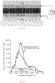
- the invention comprises a photodetector or photovoltaic device comprising a light transmissive substrate 1, a first part 2A of the light transmissive layered structure 2 overlying the substrate 1, a light transmissive first electrical contact 3 overlying the first part of the layered structure 2A, an active region 4 overlying the first part of the layered structure, a second light transmissive electrical contact 5 overlying the active region 4, and the second part 2B of the light transmissive layered structure 2 overlying the second light transmissive electrical contact 5.
- the photovoltaic active region 4 is described as an amorphous silicon PIN junction solar cell.
- the thickness of the active region 4 ranges from 20 to 100 nanometers. It is evident to those skilled in the art that the photovoltaic active region could be of other similar material configurations, e.g. microcrystalline silicon or amorphous silicon and germanium. It is also evident to those skill in the art that the photovoltaic active region 4 could be of other material configurations such as a two-junction semiconductor cell, a triple-junction semiconductor cell, or a tandem semiconductor with a three terminal structure cell. The latter structures may contain additional light transmissive electrical contacts interlayered in the active region.
- the photovoltaic active region 4 can also be described as an organic, or partially organic type semiconductor junction including: a transparent n-type semiconductor acting as an electron transporting or an electron pass filter layer underneath an absorber layer composed of a blend of two or more organic semi-conductor materials being at least one of them an electron donor and at least one of the an electron accpetor, underneath a transparent p-type semi-conductor acting as a hole transporting or a hole pass filter layer.
- the order of the n-type and p-type filters may be interchanged.
- the n-type material layer may comprise a transparent, either homogenous or with a nanoparticle, or both, morphology layer (thickness between 1 nm and 100 nm) of either ZnO, or In doped ZnO, or Al doped ZnO, or Ga doped ZnO, or Mn doped ZnO, or TiO 2 , or SnO 2 , or Poly[(9,9-bis(3'-(N,N-dimethylamino)propyl)-2,7-fluorene)-alt-2,7-(9,9-dioctylfluorene)] (PFN), or derivatives of PFN, Polyethylenimine (PEI) and derivatives, or a combination of them, the absorber layer may be a layer (thickness between 18 nm and 200 nm) comprising the blend of two organic materials, being one of them an electron donor conjugated polymer with alternating electron-donor and electron
- the absorber layer in the partially organic type semiconductor junction for the active region 4 may comprise a blend layer (thickness between 18 nm and 200 nm) of two organic materials, being one of them a ⁇ -PTPTBT polymer, where the electron donating unit is a thiophene-phenylene-thiophene (TPT) and the acceptor unit is 2,1,3-benzothiadiazole (BT), and being the other one C 60 or a soluble derivative of the fullerene family of compounds, or a nonfullerene electron acceptor.
- TPT thiophene-phenylene-thiophene
- BT 2,1,3-benzothiadiazole
- the absorber layer in the partially organic type semiconductor junction for the active region 4 may comprise a blend layer (thickness between 18 nm and 200 nm) of two organic materials, being the electron donor the polymer poly[(2,6-(4,8- bis(5-(2-ethylhexyl)thiophen-2-yl)benzo[1,2-b:4,5-b']- dithiophene))-alt-(5,5-(1',3'-di-2-thienyl-5',7'-bis(2-ethylhexyl)benzo[1',2'-c:4',5'-c']dithiophene-4,8-dione))] (PBDB-T), and the electron acceptor the non-fullerene acceptor 3,9-bis(2-methylene-(3-(1,1-dicyanomethylene)indanone))-5,5,11,11-tetrakis(4- hexylphenyl)dithi
- the absorber layer in the partially organic type semiconductor junction for the active region 4 can be composed of a blend layer (thickness between 18 nm and 200 nm) of two organic materials, being one of them polythiophene polymer (P3HT) or an oligomer of the thiopene unit, and the other one C 60 or a soluble derivative of the fullerene family of compounds, or a nonfullerene electron acceptor.
- P3HT polythiophene polymer
- oligomer of the thiopene unit the other one C 60 or a soluble derivative of the fullerene family of compounds, or a nonfullerene electron acceptor.
- the active region 4 comprises an intrinsic type conductivity region of amorphous silicon having a good optical absorption and regions of opposite conductivity type forming a p-i-n type semiconductor.
- the first part 2A of the layered structure comprises at least one or many sub-layers of light transmissive materials as dielectric materials or thin metals. It is understood that what differentiates a sub-layer from another sub-layer of the layered structure in the present invention is the index of refraction. It is also understood that two sub-layers become indistinguishable when the index of refraction is the same at all wavelengths.
- the index of the first sub-layer of such first part 2A of the layered structure overlying the substrate material 1 must have an index of refraction different than the index of the second sub-layer overlying the first.
- the second sub-layer overlying the first must have an index of refraction different than the first sub-layer underlying the second and the third sub-layer overlying the second sub-layer. This sequencing is repeated up to the last sub-layer underlying the first transmissive electrical contact 3.
- the second part 2B of the layered structure comprises at least one or many sub-layers of light transmissive materials as dielectric materials or thin metals.
- the index of the first sub-layer of such second layered structure overlying the second electrical contact must have an index of refraction different than the one of the second sub-layer overlying the first.
- the second sub-layer overlying the first must have an index of refraction different than the first sub-layer underlying such second sub-layer and the third sub-layer overlying such second sub-layer. This sequencing is repeated up to the last sub-layer.
- the total number of sub-layers, material and thickness of each sub-layer are chosen to maximize the performance of photovoltaic device.
- the thickness of each sub-layer may range from one atom thick layer to 200 nm.
- the exact selection of material and thickness for each sub-layer depends on the constants of the of rest of sub-layers and the constants of the other layers of the device 3, 4, and 5. Maximize the performance of the device must be understood as to achieve an optimal light localization that maximizes the efficiency of light to electricity conversion, minimizes the fabrication cost of the device, and optimizes other useful properties of the photovoltaic device as the light transmission in the visible region, filtering in the UV or Infrared, or the color hue of the vision obtained by the human eye through the device.
- An optimal light localization must be understood as limited to the spectral region of maximum sun light absorption by amorphous silicon, the active material 4.
- the substrate 1 of the invention can be of any light transmissive rigid or flexible material on which the photovoltaic cell can be grown upon as glass, crystal, transparent metal, semiconductor, plastic. Examples of these materials are silica (SiO2), borosilicate (BK7) and PET.
- the first and second transmissive electrical contacts (3 and 5) may comprise a thin metal layer from the elements of the group of Ag, Al, Au, Ti, Ni, Cu,... or combinations thereof, or a transparent conductive oxide layer from the group of ITO, ZnO, AI:ZnO, SnO2, FTO, or conductive polymers such as PEDOT, PEDOT:PSS, PEDOT-TMA or a carbon nanotube, or a graphene layer.
- Each sub-layer of the layered structure 2 may comprise a transparent inorganic material such as TiO2, SiO2, SiN1.3:H, SiO2:F, Ta2O5, ZnO, Al2O3, ZnS, MgF2,CaF2,or mixtures of them.
- the sub-layers may comprise polymer materials such as PMMA, Polystyrene, PET, or mixtures of polymers and inorganic materials, polymers and thin metals, or inorganic materials and thin metals.
- the solid line in Fig. 2 represents the absorbed number of photons under AM1.5 illumination of 1 sun as a function of the wavelength of the incident light for the cell of the present invention.
- the dashed line represents the photo-carrier generation efficiency under the same illumination conditions as a function of the wavelength of the incident light for the comparison cell.
- the body of the cell of the present invention comprises a silica glass substrate.
- a 260 nm thick AZO electrode underlying an 40 nm p-i-n amorphous silicon diode, a 90 nm ITO electrode overlying the p-i-n diode, and a six sub-layer structure separated into two parts.
- the first part 2A is composed of a 10 nm sub-layer 2A1 of TiO2, overlying the substrate and underlying a 32.5 nm SiO2 sub-layer 2A2, underlying a second 15 nm TiO2 sub-layer 2A3, which is underlying the AZO electrode.
- the second part 2B is composed of a 50 nm TiO2 sub-layer 2B1 overlying the ITO electrode, a 97.5 nm SiO2 sub-layer 2B2 overlying the first TiO2 sub-layer 2B1 of that second part and underlying the last 50 nm TiO2 sub-layer 2B3 which is the last layer that also isolates the rest of the device from air.
- the body of the comparison cell is the same except that it does not include the layered structure 2 for light localization.
- Figure 4 is a graph comparing the predicted external quantum efficiency and short circuit current density of the invention (solid line) with a semi-transparent cell which does not include the structure 2 (dashed line), while Figure 5 is a graph comparing the predicted light transmission of the invention (solid line) with a semi-transparent cell which does not include the structure 2 (dashed line).
- the embodiment of the invention comprises: a light transmissive substrate made of glass with an index of refraction of approximately 1.54, a first part 2A of the light transmissive layered structure 2 overlying the substrate 1 composed of a 14.5 nm sub-layer of TiO2 and a 5 nm sub-layer of ZnO, a light transmissive first electrical contact 3 composed of a 7 nm Ag layer overlying the first part of the layered structure 2A, an active region 4 overlying the first part of the layered structure, comprising an electron transporting layer comprising a 15 nm layer of n-type ZnO, an 80 nm blend layer comprising the polymer PTB7-Th and the fullerene derivative PC 71 BM mixed in a 1:2 weight ratio, and a hole transporting layer comprising a 5 nm layer of p-type MoO 3 , a second light transmissive electrical contact 5 composed of a 10 nm Ag layer overlying the
- the embodiment of the semi-transparent cell which does not include the structure 2 is the same as the embodiment of the invention except that the structure 2 is eliminated and the absorber layer is 95 nm thick instead of 80 nm.
- the invention allows for a tremendous 25% increase in short circuit current density using an absorber layer which is 15 nm thinner than the absorber layer for the semi-transparent cell which does not include the structure 2.
- light transmission in the visible is very similar for both embodiments except for a small reduction in the red for the embodiment of the invention that will give that cell a slightly bluish hue.
Landscapes
- Physics & Mathematics (AREA)
- Electromagnetism (AREA)
- Photovoltaic Devices (AREA)
Abstract
A photovoltaic device cell comprising a first light transmissive electrical contact, an active region, a second light transmissive electrical contact, and a layered structure enclosing the active region, the layered structure being formed of two parts, a first part underlying the first light transmissive electrical contact and a second part overlying the second electrical contact and wherein the constants of the layers in these layered structures are interdependent such that light is localized within the active region.
Description
- The present application relates to photoconversion devices such as photovoltaic cells or photodetectors. More in particular, the application is related to a light transmissive layered structure to achieve light localization in the active region of a photovoltaic device.
- Light localization has been used effectively to enhance the performance of many devices that rely on an efficient interaction between light and matter. Light localization refers to an increase of the light intensity in a local region on the axis or longitudinal direction of the light propagation. Light localization can be achieved using Fabry-Perot type cavities, periodic gratings, photonic crystals, micro-resonators, periodic or non-periodic distribution of layers that alternate high and low index of refraction materials, and many other distributions of dielectric or metallic materials. In photovoltaic devices, photons (light) absorbed by the photovoltaic active material are converted to electron-hole pairs or charged carriers. An effective absorption of the light by such photovoltaic material can be achieved when the thickness of such layer is longer than the material photon absorption length in a broad range of the solar spectrum. This length varies from one photovoltaic material to another but, an effective absorption of photons in a broad range of the solar spectrum may require the use of 10s or 100s of microns of active material. Several drawbacks are linked to the use of such thick material layers as, an increase in material cost, an increase in electron-hole recombination due to the finite carrier drift or diffusion length, or a reduction in transparency for cells meant to be used as windows, for instance, in Building integrated photovoltaics (BIPV). Several techniques to increase light absorption in thin-film devices and methods of manufacturing the same have been disclosed in patents and journal publications.
-
U.S. Pat. No. 4,126,150 sets forth a transparent layer which thickness is adjusted to increase the solar radiation absorption efficiency. - J. Meier et al. Thin Solid Films 451-452 (2004) 518-524 report on the use of an antireflection multilayer design in order to couple more light inside an amorphous silicon pi-n cell.
-
U.S. Pat. No. 4,442,310 discloses a spacer layer in between the back metal contact and the body of the active material to reduce the reflectivity of the photovoltaic cell in a particular wavelength range. A similar approached applied to dye sensitized solar cells and using a one-dimensional photonic crystal to achieve reflection was disclosed inUS 2011/0030792 A1 . - R. R. Lunt et al. Applied Physics Letters 98 (2011) Art. No. 113305 report on the use of distributed Bragg reflector mirror to increase reflectivity in the infrared which subsequently increases the efficiency of a low efficiency transparent organic solar cell. In amorphous silicon cells, typically, an increase in the absorption light trapping is achieved by introducing a textured substrate and special back reflectors. This leads to a large suppression of losses due to optical reflection outside the cell or to light transmission to the back contact as described by Ruud E. I. Schropp and M. Zeman in "Amorphous and Microcrystalline Silicon Solar Cells," published by Kluwer Academic Publishers (1998) p. 160-162. However, textured substrates or textured layers are a source of diffusion which in a transparent cell to be used for instance, in automobile windshields or in architectural installations would lead to a loss of clear vision.
- The main object of the present invention is to increase absorption in a photodetector or photovoltaic cell. This effect is achieved by using an optical layered structure to achieve light localization in the photovoltaic active region of the device. Light localization as opposed to conventional light trapping offers the possibility to increase absorption without light diffusion or scattering. The photodetector or photovoltaic cell comprises a first light transmissive electrical contact underlying one surface of the active photosensitive region, a photosensitive region, a light transmissive electrical contact overlying the opposite surface of the photosensitive region, and a light transmissive layered structure separated in two layered parts, one part underlying the first electrical contact and a second part overlying the second electrical contact.
- To complete the description and in order to provide for a better understanding of the invention, a set of drawings is provided.
-
Figure 1 is the cross-sectional representation of the photovoltaic device of the present invention. -
Figure 2 is a graph comparing the absorbed photons, which is proportional to the photo-carrier generation efficiency, for the photovoltaic cell of the present invention when the active material is amorphous silicon to a cell with no light localization with the same thickness of amorphous silicon as active material. -
Figure 3 is the cross-sectional representation of the best mode layered structure for light localization. -
Figure 4 is a graph comparing the predicted external quantum efficiency and short circuit current density of the present invention with a semi-transparent cell which does not include the light transmissive layered structure of the present invention. -
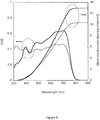
Figure 5 is a graph comparing the predicted light transmission of the present invention with a semi-transparent cell which does not include the light transmissive layered structure of the present invention. - The present invention integrates a photodetector or photovoltaic cell in a structure of light
transmissive parts 2 that can be comprised of sub-layers, where the index of refraction of a given sub-layer is different than the index of refraction of the adjacent layer. It is understood that sub-layers become indistinguishable when the index of refraction is the same at all wavelengths. The thickness of each part (2A, 2B) is determined to effectively localize light (photons) in the active region of the device depending on the number of sub-layers. Such a design allows to achieve light localization in a broad wavelength range within the absorption band of theactive region 4. Byactive region 4 is meant the portion of the device in which light (or photons) can be absorbed to generate carriers. The light transmissive layered structure comprises at least two parts, onepart 2A underlying and in contact the first lighttransmissive electrode 3, which is underlying theactive region 4, and asecond part 2B overlying and in contact with the secondtransmissive electrode 5 which is overlying theactive region 4. However, the layered structure acts as a single element with one purpose, i.e. localizing light. To localize light effectively the constants of both parts must be interdependent. - In one embodiment, the invention comprises a photodetector or photovoltaic device comprising a light
transmissive substrate 1, afirst part 2A of the light transmissivelayered structure 2 overlying thesubstrate 1, a light transmissive firstelectrical contact 3 overlying the first part of thelayered structure 2A, anactive region 4 overlying the first part of the layered structure, a second light transmissiveelectrical contact 5 overlying theactive region 4, and thesecond part 2B of the light transmissivelayered structure 2 overlying the second light transmissiveelectrical contact 5. - The photovoltaic
active region 4 is described as an amorphous silicon PIN junction solar cell. The thickness of theactive region 4 ranges from 20 to 100 nanometers. It is evident to those skilled in the art that the photovoltaic active region could be of other similar material configurations, e.g. microcrystalline silicon or amorphous silicon and germanium. It is also evident to those skill in the art that the photovoltaicactive region 4 could be of other material configurations such as a two-junction semiconductor cell, a triple-junction semiconductor cell, or a tandem semiconductor with a three terminal structure cell. The latter structures may contain additional light transmissive electrical contacts interlayered in the active region. - The photovoltaic
active region 4 can also be described as an organic, or partially organic type semiconductor junction including: a transparent n-type semiconductor acting as an electron transporting or an electron pass filter layer underneath an absorber layer composed of a blend of two or more organic semi-conductor materials being at least one of them an electron donor and at least one of the an electron accpetor, underneath a transparent p-type semi-conductor acting as a hole transporting or a hole pass filter layer. The order of the n-type and p-type filters may be interchanged. - For the partially organic type semiconductor junction in 4, the n-type material layer may comprise a transparent, either homogenous or with a nanoparticle, or both, morphology layer (thickness between 1 nm and 100 nm) of either ZnO, or In doped ZnO, or Al doped ZnO, or Ga doped ZnO, or Mn doped ZnO, or TiO2, or SnO2, or Poly[(9,9-bis(3'-(N,N-dimethylamino)propyl)-2,7-fluorene)-alt-2,7-(9,9-dioctylfluorene)] (PFN), or derivatives of PFN, Polyethylenimine (PEI) and derivatives, or a combination of them, the absorber layer may be a layer (thickness between 18 nm and 200 nm) comprising the blend of two organic materials, being one of them an electron donor conjugated polymer with alternating electron-donor and electron-acceptor monomers where the donor is a derivative of benzo[1,2-b:4,5-b']dithiophene, whereas as for the acceptor many different types of compounds can be used, for example, though not exclusively, thiophene, benzothiadiazole or diketopyrrolopyrrole derivatives, such as for instance, the electron donor conjugated polymer poly[4,8-bis(5-(2-ethylhexyl)thiophen-2-yl)benzo[1,2-b;4,5-b']dithiophene-2,6-diyl-alt-(4-(2-ethylhexyl)-3-fluorothieno[3,4-b]thiophene-)-2-carboxylate-2-6-diyl)] (PTB7-Th), and being the other organic material in the blend an electron acceptor as C60, or a soluble derivative of the fullerene family of compounds, or a non-fullerene electron acceptor, such as for instance, IHIC which is based on an electron-rich fused hexacyclic unit end-capped with an electron-
deficient unit 1,1-dicyano-methylene-3-indanone (IC), or ATT-1 containing an effective thieno[3,4-b]thiophene and 2-(1,1-dicyanomethylene)rhodanine combination, and the p-type material may comprise a transparent either homogenous or with a nanoparticle morphology layer (thickness between 1 nm and 100 nm) of either MoO3, or PEDOT:PSS, PCPDTPhSO3Na (CPE-K), or WO3, or NiO, PTAA, Spiro-TAD or a combination of them. - Alternatively, the absorber layer in the partially organic type semiconductor junction for the
active region 4 may comprise a blend layer (thickness between 18 nm and 200 nm) of two organic materials, being one of them a α-PTPTBT polymer, where the electron donating unit is a thiophene-phenylene-thiophene (TPT) and the acceptor unit is 2,1,3-benzothiadiazole (BT), and being the other one C60 or a soluble derivative of the fullerene family of compounds, or a nonfullerene electron acceptor. - Alternatively, the absorber layer in the partially organic type semiconductor junction for the
active region 4 may comprise a blend layer (thickness between 18 nm and 200 nm) of two organic materials, being the electron donor the polymer poly[(2,6-(4,8- bis(5-(2-ethylhexyl)thiophen-2-yl)benzo[1,2-b:4,5-b']- dithiophene))-alt-(5,5-(1',3'-di-2-thienyl-5',7'-bis(2-ethylhexyl)benzo[1',2'-c:4',5'-c']dithiophene-4,8-dione))] (PBDB-T), and the electron acceptor thenon-fullerene acceptor 3,9-bis(2-methylene-(3-(1,1-dicyanomethylene)indanone))-5,5,11,11-tetrakis(4- hexylphenyl)dithieno[2,3-d:2',3'-d']-s-indaceno[1,2-b:5,6-b']- dithiophene (ITIC). - Alternatively, the absorber layer in the partially organic type semiconductor junction for the
active region 4 can be composed of a blend layer (thickness between 18 nm and 200 nm) of two organic materials, being one of them polythiophene polymer (P3HT) or an oligomer of the thiopene unit, and the other one C60 or a soluble derivative of the fullerene family of compounds, or a nonfullerene electron acceptor. - In
Fig. 1 theactive region 4 comprises an intrinsic type conductivity region of amorphous silicon having a good optical absorption and regions of opposite conductivity type forming a p-i-n type semiconductor. Thefirst part 2A of the layered structure comprises at least one or many sub-layers of light transmissive materials as dielectric materials or thin metals. It is understood that what differentiates a sub-layer from another sub-layer of the layered structure in the present invention is the index of refraction. It is also understood that two sub-layers become indistinguishable when the index of refraction is the same at all wavelengths. The index of the first sub-layer of suchfirst part 2A of the layered structure overlying thesubstrate material 1 must have an index of refraction different than the index of the second sub-layer overlying the first. The second sub-layer overlying the first must have an index of refraction different than the first sub-layer underlying the second and the third sub-layer overlying the second sub-layer. This sequencing is repeated up to the last sub-layer underlying the first transmissiveelectrical contact 3. Thesecond part 2B of the layered structure comprises at least one or many sub-layers of light transmissive materials as dielectric materials or thin metals. The index of the first sub-layer of such second layered structure overlying the second electrical contact must have an index of refraction different than the one of the second sub-layer overlying the first. The second sub-layer overlying the first must have an index of refraction different than the first sub-layer underlying such second sub-layer and the third sub-layer overlying such second sub-layer. This sequencing is repeated up to the last sub-layer. The total number of sub-layers, material and thickness of each sub-layer are chosen to maximize the performance of photovoltaic device. The thickness of each sub-layer may range from one atom thick layer to 200 nm. The exact selection of material and thickness for each sub-layer depends on the constants of the of rest of sub-layers and the constants of the other layers of thedevice active material 4. Such spectral region comprises the visible and near infra-red portions of the light spectrum which wavelength ranges from 400 to 800 nanometers. Thesubstrate 1 of the invention can be of any light transmissive rigid or flexible material on which the photovoltaic cell can be grown upon as glass, crystal, transparent metal, semiconductor, plastic. Examples of these materials are silica (SiO2), borosilicate (BK7) and PET. - The first and second transmissive electrical contacts (3 and 5) may comprise a thin metal layer from the elements of the group of Ag, Al, Au, Ti, Ni, Cu,... or combinations thereof, or a transparent conductive oxide layer from the group of ITO, ZnO, AI:ZnO, SnO2, FTO, or conductive polymers such as PEDOT, PEDOT:PSS, PEDOT-TMA or a carbon nanotube, or a graphene layer. Each sub-layer of the
layered structure 2 may comprise a transparent inorganic material such as TiO2, SiO2, SiN1.3:H, SiO2:F, Ta2O5, ZnO, Al2O3, ZnS, MgF2,CaF2,or mixtures of them. Alternatively the sub-layers may comprise polymer materials such as PMMA, Polystyrene, PET, or mixtures of polymers and inorganic materials, polymers and thin metals, or inorganic materials and thin metals. - Referring to
Fig. 2 a comparison is shown of the absorbed number of photons which is directly proportional to the photo-carrier generation efficiency of the solar cell of the present invention to the absorbed number of photons of a similar solar cell, which does not include thelayered structure 2 for light localization. The solid line inFig. 2 represents the absorbed number of photons under AM1.5 illumination of 1 sun as a function of the wavelength of the incident light for the cell of the present invention. The dashed line represents the photo-carrier generation efficiency under the same illumination conditions as a function of the wavelength of the incident light for the comparison cell. - The absorbed number of photons of both cells is computed numerically. The body of the cell of the present invention comprises a silica glass substrate. A 260 nm thick AZO electrode underlying an 40 nm p-i-n amorphous silicon diode, a 90 nm ITO electrode overlying the p-i-n diode, and a six sub-layer structure separated into two parts. Referring to
Figure 3 , thefirst part 2A is composed of a 10 nm sub-layer 2A1 of TiO2, overlying the substrate and underlying a 32.5 nm SiO2 sub-layer 2A2, underlying a second 15 nm TiO2 sub-layer 2A3, which is underlying the AZO electrode. Thesecond part 2B is composed of a 50 nm TiO2 sub-layer 2B1 overlying the ITO electrode, a 97.5 nm SiO2 sub-layer 2B2 overlying the first TiO2 sub-layer 2B1 of that second part and underlying the last 50 nm TiO2 sub-layer 2B3 which is the last layer that also isolates the rest of the device from air. The body of the comparison cell is the same except that it does not include thelayered structure 2 for light localization. -
Figure 4 is a graph comparing the predicted external quantum efficiency and short circuit current density of the invention (solid line) with a semi-transparent cell which does not include the structure 2 (dashed line), whileFigure 5 is a graph comparing the predicted light transmission of the invention (solid line) with a semi-transparent cell which does not include the structure 2 (dashed line). For these graphs inFigures 4 and5 , the embodiment of the invention comprises: a light transmissive substrate made of glass with an index of refraction of approximately 1.54, afirst part 2A of the light transmissive layeredstructure 2 overlying thesubstrate 1 composed of a 14.5 nm sub-layer of TiO2 and a 5 nm sub-layer of ZnO, a light transmissive firstelectrical contact 3 composed of a 7 nm Ag layer overlying the first part of the layeredstructure 2A, anactive region 4 overlying the first part of the layered structure, comprising an electron transporting layer comprising a 15 nm layer of n-type ZnO, an 80 nm blend layer comprising the polymer PTB7-Th and the fullerene derivative PC71BM mixed in a 1:2 weight ratio, and a hole transporting layer comprising a 5 nm layer of p-type MoO3, a second light transmissiveelectrical contact 5 composed of a 10 nm Ag layer overlying theactive region 4, and thesecond part 2B of the light transmissive layeredstructure 2 overlying the second light transmissiveelectrical contact 5 composed of a 40 nm layer of MgF2, a 90 nm layer of MoO3, a 130 nm layer of MgF2, and a 110 nm layer of MoO3, and a protective glass with and index of refraction of 1.54 overlaying 2B. For these graphs inFigures 4 and5 , the embodiment of the semi-transparent cell which does not include thestructure 2 is the same as the embodiment of the invention except that thestructure 2 is eliminated and the absorber layer is 95 nm thick instead of 80 nm. Note that the invention allows for a tremendous 25% increase in short circuit current density using an absorber layer which is 15 nm thinner than the absorber layer for the semi-transparent cell which does not include thestructure 2. Note also that light transmission in the visible is very similar for both embodiments except for a small reduction in the red for the embodiment of the invention that will give that cell a slightly bluish hue. - In this text, the term "comprises" and its derivations (such as "comprising", etc.) should not be understood in an excluding sense, that is, these terms should not be interpreted as excluding the possibility that what is described and defined may include further elements. On the other hand, the invention is obviously not limited to the specific embodiment(s) described herein, but also encompasses any variations that may be considered by any person skilled in the art (for example, as regards the choice of materials, dimensions, components, configuration, etc.), within the spirit of the invention.
Claims (11)
- A photovoltaic device comprisinga first light transmissive electrical contact structured to connect the photovoltaic device to an external circuit;an active region which is made of a partially organic type semiconductor junction comprising a semi-transparent electron transporting layer underneath an absorber layer composed of a mixture of two or more organic semi-conductor materials underneath a semi-transparent hole transporting layer;a second light transmissive electrical contact structured to connect the photovoltaic device to the external circuit, wherein the first light transmissive electrical contact and the second light transmissive electrical contact are each in direct contact with the active region; anda light transmissive layered structure enclosing the active region, the light transmissive layered structure being formed of a first layered structure part and a second layered structure part, the first layered structure part underlying and directly in contact with the first light transmissive electrical contact, and the second layered structure part overlying and directly in contact with the second light transmissive electrical contact, wherein the first layered structure part and the second layered structure part act as a single element such that light is localized within the active region,wherein the first layered structure part and the second layered structure part each comprises two or more sub-layers of different transparent materials, the transparent materials are independently selected from the group consisting of TiO2, SiO2, SiN1.3:H, SiO2:F, Ta2O5, ZnO, Al2O3, ZnS, MgF2, PMMA, Polystyrene, PET, mixtures of polymers, inorganic materials, and thin metals, and each sub-layer is a continuous layer covering the entire surface area of the active region;wherein the index of refraction of a first sub-layer of transparent material of both first layered structure part and the second layered structure part is different from an adjacent sub-layer of transparent material; andwherein the first and the second light transmissive electrical contacts comprise a thin layer of a metal selected from the group consisting of Ag, Al, Au, Ti, Ni, Cu, and combinations thereof.
- A photovoltaic device as in claim 1 wherein the active region is made of a two-junction semiconductor type cell.
- A photovoltaic device as in claim 1 wherein the active region is made of a triple-junction semiconductor type cell.
- A photovoltaic device as in claim 1 wherein the active region is made of tandem semiconductor type cell with a three terminal structure comprising additional light transmissive electrical contacts interlayered in the active region.
- A photovoltaic device as in claim 1 having a light transmissive substrate underlying the first layered structure.
- A photodetector comprising the photovoltaic device of claim 1.
- The photovoltaic device according to claim 1, wherein the first layered structure part comprises a first sub-layer of TiO2, a second sub-layer of SiO2, and a third sub-layer of TiO2.
- The photovoltaic device according to claim 1, wherein each sub-layer consists of a single material independently selected from the group consisting of TiO2, SiO2, SiN1.3:H, SiO2:F, Ta2O5, ZnO, Al2O3, ZnS, and MgF.
- A photovoltaic device according to claim 1 where the thickness of the active region is between 20 nm and 200 nm.
- A photovoltaic device according to claim 1 wherein a light transmissive layered structure enclosing the active region contains one or more inorganic material sub-layers consisting of MoO3.
- A photovoltaic device according to claim 1 wherein the order of the semi-transparent electron and hole transporting layers in the active region is interchanged.
Applications Claiming Priority (1)
| Application Number | Priority Date | Filing Date | Title |
|---|---|---|---|
| US15/723,923 US10205042B2 (en) | 2012-01-26 | 2017-10-03 | Photoconversion device with enhanced photon absorption |
Publications (1)
| Publication Number | Publication Date |
|---|---|
| EP3467881A1 true EP3467881A1 (en) | 2019-04-10 |
Family
ID=63787740
Family Applications (1)
| Application Number | Title | Priority Date | Filing Date |
|---|---|---|---|
| EP18198354.5A Withdrawn EP3467881A1 (en) | 2017-10-03 | 2018-10-02 | Photoconversion device with enhanced photon absorption |
Country Status (1)
| Country | Link |
|---|---|
| EP (1) | EP3467881A1 (en) |
Citations (5)
| Publication number | Priority date | Publication date | Assignee | Title |
|---|---|---|---|---|
| US4126150A (en) | 1977-03-28 | 1978-11-21 | Rca Corporation | Photovoltaic device having increased absorption efficiency |
| US4442310A (en) | 1982-07-15 | 1984-04-10 | Rca Corporation | Photodetector having enhanced back reflection |
| US20110030792A1 (en) | 2008-04-18 | 2011-02-10 | Hernan Miguez | Solar to electric energy conversion device |
| US20130192666A1 (en) * | 2012-01-26 | 2013-08-01 | Universitat Politecnica De Catalunya | Photoconversion device with enhanced photon absorption |
| US20170241836A1 (en) * | 2014-10-07 | 2017-08-24 | Technische Universität Dresden | Apparatus for spectrometrically capturing light with a photodiode which is monolithically integrated in the layer structure of a wavelength-selective filter |
-
2018
- 2018-10-02 EP EP18198354.5A patent/EP3467881A1/en not_active Withdrawn
Patent Citations (5)
| Publication number | Priority date | Publication date | Assignee | Title |
|---|---|---|---|---|
| US4126150A (en) | 1977-03-28 | 1978-11-21 | Rca Corporation | Photovoltaic device having increased absorption efficiency |
| US4442310A (en) | 1982-07-15 | 1984-04-10 | Rca Corporation | Photodetector having enhanced back reflection |
| US20110030792A1 (en) | 2008-04-18 | 2011-02-10 | Hernan Miguez | Solar to electric energy conversion device |
| US20130192666A1 (en) * | 2012-01-26 | 2013-08-01 | Universitat Politecnica De Catalunya | Photoconversion device with enhanced photon absorption |
| US20170241836A1 (en) * | 2014-10-07 | 2017-08-24 | Technische Universität Dresden | Apparatus for spectrometrically capturing light with a photodiode which is monolithically integrated in the layer structure of a wavelength-selective filter |
Non-Patent Citations (6)
| Title |
|---|
| J. MEIER ET AL., THIN SOLID FILMS, vol. 451-452, 2004, pages 518 - 524 |
| MANTILLA-PEREZ, PAOLA: "Oxide Layers in Organic Solar Cells for an Optimal Photon Management", 20 September 2017 (2017-09-20), pages p. 481 - 499, XP009510662, ISBN: 978-0-12-811165-9, Retrieved from the Internet <URL:https://www.sciencedirect.com/science/article/pii/B9780128111659000120> [retrieved on 20190122] * |
| R. R. LUNT ET AL., APPLIED PHYSICS LETTERS, vol. 98, 2011 |
| ROMERO-GÓMEZ PABLO ET AL: "Semi-transparent polymer solar cells", JOURNAL OF PHOTONICS FOR ENERGY, SOCIETY OF PHOTO-OPTICAL INSTRUMENTATION ENGINEERS, 1000 20TH ST. BELLINGHAM WA 98225-6705 USA, vol. 5, no. 1, 15 February 2015 (2015-02-15), pages 57212-1 - 57212-13, XP060053829, DOI: 10.1117/1.JPE.5.057212 * |
| RUUD E. I. SCHROPP; M. ZEMAN: "Amorphous and Microcrystalline Silicon Solar Cells", 1998, KLUWER ACADEMIC PUBLISHERS, pages: 160 - 162 |
| YUELIN PENG ET AL: "ITO-Free Transparent Organic Solar Cell with Distributed Bragg Reflector for Solar Harvesting Windows", ENERGIES, vol. 10, no. 5, 17 May 2017 (2017-05-17), pages 707-1 - 707-13, XP055546363, DOI: 10.3390/en10050707 * |
Similar Documents
| Publication | Publication Date | Title |
|---|---|---|
| US11424423B2 (en) | Transparent photovoltaic cells | |
| US10205042B2 (en) | Photoconversion device with enhanced photon absorption | |
| CN104134750B (en) | Semi-transparent Mingguang City's conversion devices | |
| Zhang et al. | Colorful semitransparent polymer solar cells employing a bottom periodic one-dimensional photonic crystal and a top conductive PEDOT: PSS layer | |
| ES2369583T3 (en) | FIBROUS PHOTOVOLTAIC DEVICES AND APPLICATIONS OF THE SAME. | |
| KR102170089B1 (en) | Organic photosensitive devices with reflectors | |
| CN101911331B (en) | Lateral organic optoelectronic devices and applications thereof | |
| Salehin et al. | Design of blue, green and red colorful semitransparent films using Ag/SnO2/Ag color filter for integrated into solar cells | |
| Lee et al. | Microcavity-integrated colored semitransparent hybrid photovoltaics with improved efficiency and color purity | |
| US9842947B2 (en) | Photoconversion device with enhanced photon absorption | |
| EP3467881A1 (en) | Photoconversion device with enhanced photon absorption | |
| US11444256B2 (en) | Filter-free tunable spectrum photodetectors | |
| US9748423B2 (en) | Photovoltaic device with fiber array for sun tracking | |
| Rani et al. | 1D‐Photonic Crystals Enabling Selective Chromaticity for Colored Perovskite Solar Cells | |
| CN112014909A (en) | Indoor organic solar cell color rendering regulation and control device based on one-dimensional photonic crystals and application | |
| HK1192649B (en) | Transparent photovoltaic cells | |
| HK1192649A (en) | Transparent photovoltaic cells |
Legal Events
| Date | Code | Title | Description |
|---|---|---|---|
| PUAI | Public reference made under article 153(3) epc to a published international application that has entered the european phase |
Free format text: ORIGINAL CODE: 0009012 |
|
| STAA | Information on the status of an ep patent application or granted ep patent |
Free format text: STATUS: THE APPLICATION HAS BEEN PUBLISHED |
|
| AK | Designated contracting states |
Kind code of ref document: A1 Designated state(s): AL AT BE BG CH CY CZ DE DK EE ES FI FR GB GR HR HU IE IS IT LI LT LU LV MC MK MT NL NO PL PT RO RS SE SI SK SM TR |
|
| AX | Request for extension of the european patent |
Extension state: BA ME |
|
| STAA | Information on the status of an ep patent application or granted ep patent |
Free format text: STATUS: THE APPLICATION IS DEEMED TO BE WITHDRAWN |
|
| 18D | Application deemed to be withdrawn |
Effective date: 20191011 |