EP3467526A1 - Switch failure detection system - Google Patents
Switch failure detection system Download PDFInfo
- Publication number
- EP3467526A1 EP3467526A1 EP18198010.3A EP18198010A EP3467526A1 EP 3467526 A1 EP3467526 A1 EP 3467526A1 EP 18198010 A EP18198010 A EP 18198010A EP 3467526 A1 EP3467526 A1 EP 3467526A1
- Authority
- EP
- European Patent Office
- Prior art keywords
- time varying
- varying signal
- fault
- signal
- analysis module
- Prior art date
- Legal status (The legal status is an assumption and is not a legal conclusion. Google has not performed a legal analysis and makes no representation as to the accuracy of the status listed.)
- Granted
Links
Images




Classifications
-
- G—PHYSICS
- G01—MEASURING; TESTING
- G01R—MEASURING ELECTRIC VARIABLES; MEASURING MAGNETIC VARIABLES
- G01R31/00—Arrangements for testing electric properties; Arrangements for locating electric faults; Arrangements for electrical testing characterised by what is being tested not provided for elsewhere
- G01R31/327—Testing of circuit interrupters, switches or circuit-breakers
-
- G—PHYSICS
- G01—MEASURING; TESTING
- G01R—MEASURING ELECTRIC VARIABLES; MEASURING MAGNETIC VARIABLES
- G01R31/00—Arrangements for testing electric properties; Arrangements for locating electric faults; Arrangements for electrical testing characterised by what is being tested not provided for elsewhere
- G01R31/327—Testing of circuit interrupters, switches or circuit-breakers
- G01R31/3277—Testing of circuit interrupters, switches or circuit-breakers of low voltage devices, e.g. domestic or industrial devices, such as motor protections, relays, rotation switches
- G01R31/3278—Testing of circuit interrupters, switches or circuit-breakers of low voltage devices, e.g. domestic or industrial devices, such as motor protections, relays, rotation switches of relays, solenoids or reed switches
-
- G—PHYSICS
- G01—MEASURING; TESTING
- G01R—MEASURING ELECTRIC VARIABLES; MEASURING MAGNETIC VARIABLES
- G01R31/00—Arrangements for testing electric properties; Arrangements for locating electric faults; Arrangements for electrical testing characterised by what is being tested not provided for elsewhere
- G01R31/327—Testing of circuit interrupters, switches or circuit-breakers
- G01R31/3271—Testing of circuit interrupters, switches or circuit-breakers of high voltage or medium voltage devices
- G01R31/3275—Fault detection or status indication
-
- G—PHYSICS
- G01—MEASURING; TESTING
- G01R—MEASURING ELECTRIC VARIABLES; MEASURING MAGNETIC VARIABLES
- G01R31/00—Arrangements for testing electric properties; Arrangements for locating electric faults; Arrangements for electrical testing characterised by what is being tested not provided for elsewhere
- G01R31/327—Testing of circuit interrupters, switches or circuit-breakers
- G01R31/3277—Testing of circuit interrupters, switches or circuit-breakers of low voltage devices, e.g. domestic or industrial devices, such as motor protections, relays, rotation switches
Definitions
- the present invention is directed to the detection and identification of failed switches in electrical systems. More particularly, the present invention is directed to series switch failure detection and identification.
- the solution is provided by a method of determining a fault in two or more series switches of an electrical system.
- the electrical system includes, at least one AC power source, at least one sensor, at least two series switches, and a fault analysis module including a processor and a memory.
- the method includes applying, by the at least one AC power source, at least one time varying signal to the electrical system.
- the method further includes receiving, by the fault analysis module, at least one measurement, from the at least one sensor, of the at least one time varying signal, at, at least one node of the electrical system.
- the method further includes receiving, by the fault analysis module, at least one predetermined signal parameter and determining, by the fault analysis module, the presence of a fault, based on the at least one measurement and the at least one predetermined signal parameter.
- the electrical system may comprise at least two capacitors, each one of the series switches being connected in parallel with a corresponding one of the capacitors. The capacitors may have different values of capacitance to one another.
- a switch failure detection system capable of identifying a failed switch in an electrical system.
- Embodiments of the present disclosure for example, in comparison to concepts failing to include one or more of the features disclosed herein, provide a switch failure detection system capable of analyzing the impedance of an electrical system to isolate a failed switch.
- FIG. 1 A block diagram of an electrical system 100 is shown in FIG. 1 .
- a load 110 having a power source 115 (e.g., 50-60 Hz AC) selectively communicatively connected thereto via a switching circuit 120 including at least two series switches.
- the switching circuit 120 may include at least one one-time switch 122 configured to selectively connect a circuit to the load 110 including at least one primary switch 124 and/or at least one secondary switch 126.
- the at least two series switches includes the at least one primary switch 124 and/or at least one secondary switch 126.
- the at least two series switches includes the at least one primary switch 124.
- the secondary switch 126 may be configured to selectively connect the power source 115 to the load 110 via a pathway separate from the primary switch 124.
- the at least one one-time switch 122 selectively connects a circuit to the load 110 which does not include the primary switch 124.
- the at least one one-time switch 122 selectively connects the circuit to the load 110 which includes the secondary switch 126 and does not include the primary switch 124.
- the at least one one-time switch 122 selectively connects the circuit to the load 110 which includes the secondary switch 126 and does not include the primary switch 124, after the primary switch 124 has failed.
- the circuit to the load 110 may include the secondary switch 126 and be configured to allow the operation of the electrical system 100 until the primary switch 124 is repaired and/or replaced.
- a primary switch capacitor 128 may be included in parallel with the primary switch 124.
- a secondary switch capacitor 130 may be included in parallel with the secondary switch 126.
- a fault sensor 150 may be connected to the switching circuit 120 in parallel with the at least two series switches.
- the fault sensor 150 includes a power supply 152 which further includes an energy storage unit 154 (e.g., battery, fuel cell, and/or capacitor), a switched mode power supply 156 (SMPS), and a split rail isolation transformer 158.
- a dual threshold operate/release relay emulator 160 triggers the fault sensor 150 to begin a test sequence to determine whether the switching circuit 120 is operating properly.
- the fault sensor 150 may receive an external coil input signal 162 which may cause the dual threshold operate/release relay emulator 160 to begin the test sequence.
- the fault sensor 150 further includes an isolation region 164 which is configured to shield the components therein from spurious signals that could affect the accuracy of the measurements conducted by the fault sensor 150 during the test sequence.
- the activation of the at least one primary switch 124 may initiate the test sequence.
- a delay timer 168 is also activated during the test sequence.
- the delay timer 168 delays further implementation of the test sequence for a predetermined length of time allowing the at least one primary switch 124 to close.
- a test signal 172 is applied to the load 110 by a test signal generation module 170 via a circuit including the primary switch 124.
- the signal generation module 170 may include a signal generator 174.
- An amplifier/driver 176 boosts the power of the test signal 172 and applies the test signal 172 via a signal generator coupling circuit 178 to the load 110 and switching circuit 120.
- the amplifier/driver 176 may include a push-pull amplifier.
- the signal generator coupling circuit 178 may include a voltage follower.
- the test signal exhibits a frequency of at least about 1 kilohertz (1 kHz), at least about 10 kilohertz (10 kHz), at least about 100 kilohertz (100 kHz), at least about 300 kilohertz (300 kHz), at least about 500 kilohertz (500 kHz), less than about 100 megahertz (100 MHz), less than about 10 megahertz (10 MHz), less than about 1 megahertz (1 MHz), and combinations thereof.
- the test signal 172 may be detected by a signal receiver module 180 of the fault sensor 150.
- the signal receiver module 180 may include a signal receiver coupling circuit 182, a filter module 184 which may be configured to remove spurious signals (e.g., line noise), a signal amplifier 186, and a detection circuit 188 (e.g., amplitude detection, phase angle detection, and combinations thereof).
- the signal receiver coupling circuit 182 may including a voltage follower.
- the signal amplifier 186 may include a push-pull amplifier.
- a fault analysis module 190 receives and analyzes the test signal 172 amplitude and/or phase angle measured by the detection circuit 188.
- the fault analysis module 190 may include a processor and a memory containing instructions that when executed by the processor cause the fault analysis module 190 to analyze the test signal 172 and notify a user if a fault is detected.
- a comparison module 192 compares the test signal 172 to predetermined signal parameters corresponding to the position of the at least one primary switch 124.
- a fault relay identification module 194 analyzes the test signal 172 opposite the predetermined signal parameters and determines if the at least one primary switch 124 has failed. If a plurality of the at least one primary switches 124 are present, the fault relay identification module 194 may further determine which of the at least one primary switches 124 has failed.
- the fault analysis module 190 may generate a relay fault signal 196.
- the relay fault signal 196 may be connected to a means (e.g., display, computer, wireless device (e.g., cellphone, tablet, laptop)) to notify a user of the fault.
- the fault analysis module 190 may additionally cause a one-time switch activation module 198 to activate the at least one one-time switch 122 to select an alternative circuit pathway.
- the alternative circuit pathway includes the at least one secondary switch 126.
- FIG. 2 is a schematic diagram of an example circuit 200 illustrative of series switch fault detection.
- the circuit 200 includes a grounded AC power source 210 in series with a first resistor 220.
- a node 230 is electrically connected in series with the first resistor 220.
- a first series switch 240 is electrically connected in series with the node 230.
- the first series switch 240 includes a first relay 242 in parallel with a first capacitor 244.
- a node 250 is further electrically connected in series with the first series switch 240.
- a second series switch 260 is electrically connected in series with the node 250.
- the second series switch 260 includes, a second relay 262 in parallel with a second capacitor 264.
- a node 270 is further electrically connected in series with the second series switch 260.
- a second resistor 280 is further electrically connected to the node 270.
- a sensor 290 e.g., an oscilloscope
- a capacitance of the first capacitor 244 and a capacitance of the second capacitor 264 are different.
- FIG. 3 is a data table 300 illustrating the voltages measured by the sensor 290 at node 230 and at node 270 for each of the position combinations of the first relay 242 and the second relay 262. As seen in the data of FIG. 3 , each switch combination results in a unique combination of voltages measured by the sensor 290. The uniqueness of the data resulting from the relay positions allows a user to determine to position of the relays 242, 262 based on the data. The determination of the position of the relays 242, 262 may also be automated, such as by employing the fault analysis module 190 as described in FIG. 1 .
- the data collected by the sensor 290 may be analyzed by the fault analysis module 190 to determine which relay or relays have failed (i.e. are open). The fault analysis module 190 may then generate a relay fault signal 196 to notify a user that a relay has failed.
- FIG. 4 is a schematic diagram of an example circuit 400 illustrative of series switch fault detection.
- the circuit 400 includes a grounded first AC power source 410.
- the first AC power source 410 may be a high frequency AC power source.
- high frequency it is meant a frequency greater than about 1 kilohertz (1 kHz).
- the test signal exhibits a frequency of at least about 1 kilohertz (1 kHz), at least about 10 kilohertz (10 kHz), at least about 100 kilohertz (100 kHz), at least about 300 kilohertz (300 kHz), at least about 500 kilohertz (500 kHz), less than about 100 megahertz (100 MHz), less than about 10 megahertz (10 MHz), less than about 1 megahertz (1 MHz), and combinations thereof.
- the first AC power source 410 may exhibit a frequency of at least 1 kilohertz (1 kHz), at least 3 kilohertz (3 kHz), at least 10 kilohertz (10 kHz), at least 40 kilohertz (40 kHz), at least 60 kilohertz (60 kHz), at least 100 kilohertz (100 kHz), at least 500 kilohertz (500 kHz), at least 1 gigahertz (1 GHz), and combinations thereof.
- a first resistor 420 is electrically connected in series with the first AC power source 410.
- a node A designated by 430 is electrically connected in series to the first resistor 420.
- a first capacitor 440 is electrically connected in series to the node A 430.
- a node B designated by 450 is connected in series with the first capacitor 440.
- a first inductor 460 is electrically connected to the node B 450.
- a node C designated by 470 is electrically connected in series with the first inductor 460.
- a resistor 480 is electrically connected in series to the node C 470.
- a grounded second AC power source 490 is electrically connected to the resistor 480.
- the second AC power source 490 may be a low frequency AC power source. By low frequency it is meant a frequency less than about 1 kilohertz (1 kHz).
- the second AC power source 490 may exhibit a frequency of less than 1 kilohertz (1 kHz), less than 500 hertz (500 Hz), less than 100 hertz (100 Hz), less than 65 hertz (65 Hz), less than 60 hertz (60 Hz), less than 50 hertz (50 Hz), less than 40 hertz (40 Hz), and combinations thereof.
- a first series switch 500 is electrically connected to the node B 450.
- the first series switch 500 includes, includes a first relay 502 in parallel with a first series switch capacitor 504.
- a node F designated by 510 is further electrically connected in series with the first series switch 500.
- a second series switch 520 is electrically connected in series with the node F 510.
- the second series switch 520 includes a second relay 522 in parallel with a second series switch capacitor 524.
- a node D designated by 530 is further electrically connected in series with the second series switch 520.
- a second inductor 540 is electrically connected to the node D 530.
- a node G designated by 550 is electrically connected in series to the second inductor 540.
- a grounded resistor 560 is electrically connected in series with the node G 550.
- a second capacitor 570 is electrically connected to the node D 530.
- a node E designated by 580 is electrically connected in series with the second capacitor 570.
- a grounded resistor 590 is electrically connected in series with the node E 580.
- At least one sensor may be electrically connected to the circuit 400 and configured to measure a characteristic (e.g., voltage) at one or more of the nodes 430, 450, 510, 530, 550, and/or 580.
- a capacitance of the first series switch capacitor 504 and a capacitance of the second series switch capacitor 524 are different.
- the first AC power source 410 provides a high frequency signal of about 500 kilohertz (500 kHz) and the second AC power source 490 provides a low frequency signal of about 50 hertz (50 Hz).
- FIG. 5 illustrates a sensor view 600 of data collected at various nodes of the circuit 400 with both the first relay 502 and the second relay 522 closed.
- Trace 1 601 is the waveform at node C 470.
- Trace 2 602 is the waveform at node B 450.
- Trace 3 603 is the waveform at node E 580.
- Trace 4 604 is the waveform at node G 550.
- FIG. 6 is an expanded sensor view 650 of the waveform measured at node B 450.
- the waveform of FIG. 6 illustrates the superposition of the 500 kHz signal 652 from the first AC power source 410 and the 50 Hz signal 654 from the second AC power source 490.
- the path of the signals will include at least one of the first series switch capacitor 504 and/or second series switch capacitor 524.
- the inclusion of additional capacitance in the signal path may alter the impedance encountered by the signals.
- the impedance is dependent on the frequency of the signals.
- a capacitor may act as a high pass filter. Thus, allowing a high frequency signal to pass substantially unattenuated. The same capacitor may substantially attenuate a low frequency signal.
- FIG. 7 illustrates a sensor view 700 including a left portion 701 corresponding to the waveforms with both relays 502, 522 closed.
- the sensor view 700 also includes a right portion 702 corresponding to the waveforms with the first relay 502 open and the second relay 522 closed.
- Trace 1 705 is the waveform at node B 450.
- Trace 2 706 is the waveform at node D 530.
- Trace 3 707 is the waveform at node G 550.
- Trace 4 708 is the waveform at node E 580.
- the additional capacitance present when the first relay 502 is open results in substantial attenuation of the signal.
- the waveforms generated by the first AC power source 410 and the second AC power source 490 encounter distinct impedances corresponding to the positions of the relays 502, 522.
- the distinct impedances result in distinct waveforms present at the various nodes of the circuit 400.
- a user such as a service technician, may view the waveforms to determine which of the relays is open and thus in need of repair or replacement.
- the fault analysis module 190 may analyze the waveforms to determine which relay or relays is open and is potentially in need of repair or replacement.
- the fault analysis module 190 may additionally inform a user that one or more relays may need repair or replacement.
- fault determination may be performed in electrical systems having more than two series switches.
- Fault determination and identification may be performed in systems having at least 3 series switches, at least 5 series switches, at least 7 series switches, at least 10 series switches, at least 20 series switches, or more.
- additional signal sources e.g., AC power source
- at least 3 signal sources, at least 4 signal sources, at least 5 signal sources, or more may be employed.
- the frequency of the signal sources may range from about 1 hertz (1 Hz) to at least 1 gigahertz (1 GHz), at least 2 gigahertz (2 GHz), at least 5 gigahertz (5 GHz), at least 10 gigahertz (10 GHz), or more.
- the shape of the waveform may include sinusoidal, square, and/or sawtooth.
- FIG. 8 is a flowchart 800 of a method of determining a failed switch in an electrical system.
- the at least one AC power source applies at least one time varying signal to the electrical system.
- the fault analysis module receives at least one measurement, from the at least one sensor, of the at least one time varying signal, at at least one node of the electrical system.
- the fault analysis module receives at least one predetermined signal parameter.
- the fault analysis module determines the presence of a fault, based on the at least one measurement and the at least one predetermined signal parameter.
Landscapes
- Physics & Mathematics (AREA)
- General Physics & Mathematics (AREA)
- Testing Electric Properties And Detecting Electric Faults (AREA)
- Protection Of Static Devices (AREA)
Abstract
Description
- The present invention is directed to the detection and identification of failed switches in electrical systems. More particularly, the present invention is directed to series switch failure detection and identification.
- Electrical systems typically employ multiple switches and relays to activate and/or deactivate various system components during operation. The failure of one switch may cause the entire system to be taken out of service until the failed switch is identified and replaced. Conventional processes for the identification of failed switches typically involve testing the operation of each switch individually by a technician. Individual testing may be extremely time consuming and result in the electrical system being out of service for an extended period of time.
- The solution is provided by a method of determining a fault in two or more series switches of an electrical system. The electrical system includes, at least one AC power source, at least one sensor, at least two series switches, and a fault analysis module including a processor and a memory. The method includes applying, by the at least one AC power source, at least one time varying signal to the electrical system. The method further includes receiving, by the fault analysis module, at least one measurement, from the at least one sensor, of the at least one time varying signal, at, at least one node of the electrical system. The method further includes receiving, by the fault analysis module, at least one predetermined signal parameter and determining, by the fault analysis module, the presence of a fault, based on the at least one measurement and the at least one predetermined signal parameter. The electrical system may comprise at least two capacitors, each one of the series switches being connected in parallel with a corresponding one of the capacitors. The capacitors may have different values of capacitance to one another.
- Other features and advantages of various embodiments of the present invention will be apparent from the following more detailed description, taken in conjunction with the accompanying drawings in which:
-
FIG. 1 is a block diagram of an electrical system including a series switch failure detection system, according to an embodiment.FIG. 2 is a schematic of an exemplary circuit, according to an embodiment. -
FIG. 3 is a data table of measured characteristics of the circuit ofFIG. 2 , according to an embodiment. -
FIG. 4 is a schematic of an exemplary circuit, according to an embodiment. -
FIG. 5 is an image of a multi-channel oscilloscope display of measured characteristics of the circuit ofFIG. 4 , according to an embodiment. -
FIG. 6 is an expanded view ofchannel 2 of the oscilloscope display ofFIG. 5 , according to an embodiment. -
FIG. 7 is an image of a multi-channel oscilloscope display of measured characteristics of the circuit ofFIG. 4 , according to an embodiment. -
FIG. 8 is a flow chart of a fault detection method, according to an embodiment. - Wherever possible, the same reference numbers will be used throughout the drawings to represent the same parts.
- Provided is a switch failure detection system capable of identifying a failed switch in an electrical system. Embodiments of the present disclosure, for example, in comparison to concepts failing to include one or more of the features disclosed herein, provide a switch failure detection system capable of analyzing the impedance of an electrical system to isolate a failed switch.
- A block diagram of an
electrical system 100 is shown inFIG. 1 . In the embodiment ofFIG. 1 , aload 110 having a power source 115 (e.g., 50-60 Hz AC) selectively communicatively connected thereto via aswitching circuit 120 including at least two series switches. Theswitching circuit 120 may include at least one one-time switch 122 configured to selectively connect a circuit to theload 110 including at least oneprimary switch 124 and/or at least onesecondary switch 126. In some embodiments, the at least two series switches includes the at least oneprimary switch 124 and/or at least onesecondary switch 126. In some embodiments, the at least two series switches includes the at least oneprimary switch 124. In some embodiments, thesecondary switch 126 may be configured to selectively connect thepower source 115 to theload 110 via a pathway separate from theprimary switch 124. In some embodiments, the at least one one-time switch 122 selectively connects a circuit to theload 110 which does not include theprimary switch 124. In one embodiment, the at least one one-time switch 122 selectively connects the circuit to theload 110 which includes thesecondary switch 126 and does not include theprimary switch 124. In one embodiment, the at least one one-time switch 122 selectively connects the circuit to theload 110 which includes thesecondary switch 126 and does not include theprimary switch 124, after theprimary switch 124 has failed. In an embodiment, the circuit to theload 110 may include thesecondary switch 126 and be configured to allow the operation of theelectrical system 100 until theprimary switch 124 is repaired and/or replaced. In some embodiments, aprimary switch capacitor 128 may be included in parallel with theprimary switch 124. In some embodiments, asecondary switch capacitor 130 may be included in parallel with thesecondary switch 126. - In the embodiment of
FIG. 1 , afault sensor 150 may be connected to theswitching circuit 120 in parallel with the at least two series switches. Thefault sensor 150 includes apower supply 152 which further includes an energy storage unit 154 (e.g., battery, fuel cell, and/or capacitor), a switched mode power supply 156 (SMPS), and a splitrail isolation transformer 158. A dual threshold operate/release relay emulator 160 triggers thefault sensor 150 to begin a test sequence to determine whether theswitching circuit 120 is operating properly. In some embodiments, thefault sensor 150 may receive an externalcoil input signal 162 which may cause the dual threshold operate/release relay emulator 160 to begin the test sequence. - The
fault sensor 150 further includes anisolation region 164 which is configured to shield the components therein from spurious signals that could affect the accuracy of the measurements conducted by thefault sensor 150 during the test sequence. In some embodiments, the activation of the at least oneprimary switch 124 may initiate the test sequence. - A
delay timer 168 is also activated during the test sequence. Thedelay timer 168 delays further implementation of the test sequence for a predetermined length of time allowing the at least oneprimary switch 124 to close. Following the delay period atest signal 172 is applied to theload 110 by a testsignal generation module 170 via a circuit including theprimary switch 124. Thesignal generation module 170 may include asignal generator 174. An amplifier/driver 176 boosts the power of thetest signal 172 and applies thetest signal 172 via a signalgenerator coupling circuit 178 to theload 110 andswitching circuit 120. In some embodiments, the amplifier/driver 176 may include a push-pull amplifier. In some embodiments, the signalgenerator coupling circuit 178 may include a voltage follower. In some embodiments, the test signal exhibits a frequency of at least about 1 kilohertz (1 kHz), at least about 10 kilohertz (10 kHz), at least about 100 kilohertz (100 kHz), at least about 300 kilohertz (300 kHz), at least about 500 kilohertz (500 kHz), less than about 100 megahertz (100 MHz), less than about 10 megahertz (10 MHz), less than about 1 megahertz (1 MHz), and combinations thereof. - The
test signal 172 may be detected by asignal receiver module 180 of thefault sensor 150. Thesignal receiver module 180 may include a signalreceiver coupling circuit 182, afilter module 184 which may be configured to remove spurious signals (e.g., line noise), asignal amplifier 186, and a detection circuit 188 (e.g., amplitude detection, phase angle detection, and combinations thereof). In some embodiments, the signalreceiver coupling circuit 182 may including a voltage follower. In some embodiments, thesignal amplifier 186 may include a push-pull amplifier. - A
fault analysis module 190 receives and analyzes thetest signal 172 amplitude and/or phase angle measured by thedetection circuit 188. Thefault analysis module 190 may include a processor and a memory containing instructions that when executed by the processor cause thefault analysis module 190 to analyze thetest signal 172 and notify a user if a fault is detected. Acomparison module 192 compares thetest signal 172 to predetermined signal parameters corresponding to the position of the at least oneprimary switch 124. A faultrelay identification module 194 analyzes thetest signal 172 opposite the predetermined signal parameters and determines if the at least oneprimary switch 124 has failed. If a plurality of the at least oneprimary switches 124 are present, the faultrelay identification module 194 may further determine which of the at least oneprimary switches 124 has failed. - If the
fault analysis module 190 determines at least one of the at least one primary switches has failed thefault analysis module 190 may generate arelay fault signal 196. Therelay fault signal 196 may be connected to a means (e.g., display, computer, wireless device (e.g., cellphone, tablet, laptop)) to notify a user of the fault. Thefault analysis module 190 may additionally cause a one-timeswitch activation module 198 to activate the at least one one-time switch 122 to select an alternative circuit pathway. In some embodiments, the alternative circuit pathway includes the at least onesecondary switch 126. -
FIG. 2 is a schematic diagram of anexample circuit 200 illustrative of series switch fault detection. In the example ofFIG. 2 , thecircuit 200 includes a groundedAC power source 210 in series with afirst resistor 220. Anode 230 is electrically connected in series with thefirst resistor 220. Afirst series switch 240 is electrically connected in series with thenode 230. Thefirst series switch 240 includes afirst relay 242 in parallel with afirst capacitor 244. Anode 250 is further electrically connected in series with thefirst series switch 240. Asecond series switch 260 is electrically connected in series with thenode 250. Thesecond series switch 260 includes, asecond relay 262 in parallel with asecond capacitor 264. Anode 270 is further electrically connected in series with thesecond series switch 260. Asecond resistor 280 is further electrically connected to thenode 270. A sensor 290 (e.g., an oscilloscope) is electrically connected to thecircuit 200 and configured to measure a voltage atnode 230 and atnode 270. In some embodiments, a capacitance of thefirst capacitor 244 and a capacitance of thesecond capacitor 264 are different. -
FIG. 3 is a data table 300 illustrating the voltages measured by thesensor 290 atnode 230 and atnode 270 for each of the position combinations of thefirst relay 242 and thesecond relay 262. As seen in the data ofFIG. 3 , each switch combination results in a unique combination of voltages measured by thesensor 290. The uniqueness of the data resulting from the relay positions allows a user to determine to position of therelays relays fault analysis module 190 as described inFIG. 1 . - For example, if it is desired that both
relays sensor 290 may be analyzed by thefault analysis module 190 to determine which relay or relays have failed (i.e. are open). Thefault analysis module 190 may then generate arelay fault signal 196 to notify a user that a relay has failed. -
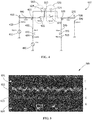
FIG. 4 is a schematic diagram of anexample circuit 400 illustrative of series switch fault detection. In the example ofFIG. 4 , thecircuit 400 includes a grounded firstAC power source 410. In some embodiments, the firstAC power source 410 may be a high frequency AC power source. By high frequency it is meant a frequency greater than about 1 kilohertz (1 kHz). In some embodiments, the test signal exhibits a frequency of at least about 1 kilohertz (1 kHz), at least about 10 kilohertz (10 kHz), at least about 100 kilohertz (100 kHz), at least about 300 kilohertz (300 kHz), at least about 500 kilohertz (500 kHz), less than about 100 megahertz (100 MHz), less than about 10 megahertz (10 MHz), less than about 1 megahertz (1 MHz), and combinations thereof. In another embodiment, the firstAC power source 410 may exhibit a frequency of at least 1 kilohertz (1 kHz), at least 3 kilohertz (3 kHz), at least 10 kilohertz (10 kHz), at least 40 kilohertz (40 kHz), at least 60 kilohertz (60 kHz), at least 100 kilohertz (100 kHz), at least 500 kilohertz (500 kHz), at least 1 gigahertz (1 GHz), and combinations thereof. Afirst resistor 420 is electrically connected in series with the firstAC power source 410. A node A designated by 430 is electrically connected in series to thefirst resistor 420. Afirst capacitor 440 is electrically connected in series to thenode A 430. A node B designated by 450 is connected in series with thefirst capacitor 440. - In the example of
FIG. 4 , afirst inductor 460 is electrically connected to thenode B 450. A node C designated by 470 is electrically connected in series with thefirst inductor 460. Aresistor 480 is electrically connected in series to thenode C 470. A grounded secondAC power source 490 is electrically connected to theresistor 480. In some embodiments, the secondAC power source 490 may be a low frequency AC power source. By low frequency it is meant a frequency less than about 1 kilohertz (1 kHz). In some embodiments, the secondAC power source 490 may exhibit a frequency of less than 1 kilohertz (1 kHz), less than 500 hertz (500 Hz), less than 100 hertz (100 Hz), less than 65 hertz (65 Hz), less than 60 hertz (60 Hz), less than 50 hertz (50 Hz), less than 40 hertz (40 Hz), and combinations thereof. - In the example of
FIG. 4 , afirst series switch 500 is electrically connected to thenode B 450. Thefirst series switch 500 includes, includes afirst relay 502 in parallel with a firstseries switch capacitor 504. A node F designated by 510 is further electrically connected in series with thefirst series switch 500. Asecond series switch 520 is electrically connected in series with thenode F 510. Thesecond series switch 520 includes asecond relay 522 in parallel with a secondseries switch capacitor 524. A node D designated by 530 is further electrically connected in series with thesecond series switch 520. Asecond inductor 540 is electrically connected to thenode D 530. A node G designated by 550 is electrically connected in series to thesecond inductor 540. A groundedresistor 560 is electrically connected in series with thenode G 550. Asecond capacitor 570 is electrically connected to thenode D 530. A node E designated by 580 is electrically connected in series with thesecond capacitor 570. A groundedresistor 590 is electrically connected in series with thenode E 580. At least one sensor (not shown) may be electrically connected to thecircuit 400 and configured to measure a characteristic (e.g., voltage) at one or more of thenodes series switch capacitor 504 and a capacitance of the secondseries switch capacitor 524 are different. - In the example of
FIG. 4 , the firstAC power source 410 provides a high frequency signal of about 500 kilohertz (500 kHz) and the secondAC power source 490 provides a low frequency signal of about 50 hertz (50 Hz). -
FIG. 5 illustrates asensor view 600 of data collected at various nodes of thecircuit 400 with both thefirst relay 502 and thesecond relay 522 closed.Trace 1 601 is the waveform atnode C 470.Trace 2 602 is the waveform atnode B 450. Trace 3 603 is the waveform atnode E 580. Trace 4 604 is the waveform atnode G 550. -
FIG. 6 , is an expandedsensor view 650 of the waveform measured atnode B 450. The waveform ofFIG. 6 illustrates the superposition of the 500 kHz signal 652 from the firstAC power source 410 and the 50 Hz signal 654 from the secondAC power source 490. - If at least one of the
first relay 502 orsecond relay 522 is opened, the path of the signals will include at least one of the firstseries switch capacitor 504 and/or secondseries switch capacitor 524. The inclusion of additional capacitance in the signal path may alter the impedance encountered by the signals. The impedance is dependent on the frequency of the signals. For example, a capacitor may act as a high pass filter. Thus, allowing a high frequency signal to pass substantially unattenuated. The same capacitor may substantially attenuate a low frequency signal.FIG. 7 illustrates asensor view 700 including aleft portion 701 corresponding to the waveforms with bothrelays sensor view 700 also includes aright portion 702 corresponding to the waveforms with thefirst relay 502 open and thesecond relay 522 closed.Trace 1 705 is the waveform atnode B 450.Trace 2 706 is the waveform atnode D 530. Trace 3 707 is the waveform atnode G 550. Trace 4 708 is the waveform atnode E 580. As seen inFIG. 7 , the additional capacitance present when thefirst relay 502 is open, results in substantial attenuation of the signal. - As illustrated in
FIG. 7 , the waveforms generated by the firstAC power source 410 and the secondAC power source 490 encounter distinct impedances corresponding to the positions of therelays circuit 400. In some embodiments, a user, such as a service technician, may view the waveforms to determine which of the relays is open and thus in need of repair or replacement. In some embodiments, thefault analysis module 190 may analyze the waveforms to determine which relay or relays is open and is potentially in need of repair or replacement. Thefault analysis module 190 may additionally inform a user that one or more relays may need repair or replacement. - In an embodiment, fault determination may be performed in electrical systems having more than two series switches. Fault determination and identification may be performed in systems having at least 3 series switches, at least 5 series switches, at least 7 series switches, at least 10 series switches, at least 20 series switches, or more. In some embodiments, additional signal sources (e.g., AC power source) may be employed to provide additional complexity to the waveform for analysis. In some embodiments, at least 3 signal sources, at least 4 signal sources, at least 5 signal sources, or more may be employed. In some embodiments, the frequency of the signal sources may range from about 1 hertz (1 Hz) to at least 1 gigahertz (1 GHz), at least 2 gigahertz (2 GHz), at least 5 gigahertz (5 GHz), at least 10 gigahertz (10 GHz), or more. In some embodiments, the shape of the waveform may include sinusoidal, square, and/or sawtooth.
-
FIG. 8 is aflowchart 800 of a method of determining a failed switch in an electrical system. Atblock 810, the at least one AC power source applies at least one time varying signal to the electrical system. Atblock 820, the fault analysis module receives at least one measurement, from the at least one sensor, of the at least one time varying signal, at at least one node of the electrical system. Atblock 830, the fault analysis module receives at least one predetermined signal parameter. Atblock 840, the fault analysis module determines the presence of a fault, based on the at least one measurement and the at least one predetermined signal parameter.
Claims (15)
- A method of determining a fault in at least one series switch (240) of an electrical system (100), the electrical system (100) including, at least one AC power source (115), at least one sensor (290), at least two series switches, and a fault analysis module (190) including a processor and a memory, the method comprising:applying, by the at least one AC power source (115), at least one time varying signal to the electrical system (100);receiving, by the fault analysis module (190), at least one measurement, from the at least one sensor (290), of the at least one time varying signal, at, at least one node (230) of the electrical system (100);receiving, by the fault analysis module (190), at least one predetermined signal parameter; anddetermining, by the fault analysis module (190), the presence of a fault, based on the at least one measurement and the at least one predetermined signal parameter.
- The method of claim 1, wherein the at least one time varying signal includes at least two time varying signals, and the at least one measurement includes at least two measurements.
- The method of claim 2, wherein the at least two measurements are determined at, at least two nodes of the electrical system.
- The method of claim 1, 2, or 3, wherein the at least one measurement includes a voltage measurement, and the predetermined signal parameter includes at least one voltage.
- The method of any preceding claim, wherein the at least one time varying signal includes a first time varying signal having a frequency less than 1 kilohertz.
- The method of claim 5, wherein the at least one time varying signal further includes a second time varying signal having a frequency greater than 1 kilohertz.
- The method of claim 6, wherein the at least one time varying signal further includes a third time varying signal having a frequency different from the first time varying signal and the second time varying signal.
- The method of claim 1, further comprising notifying a user of the presence of a fault.
- The method of claim 1, wherein the time varying signal includes a sinusoidal waveform, square waveform, or sawtooth waveform.
- A series switch (240) fault detection system, including at least two series switches, a processor and a memory containing instructions that when executed by the processor cause the system to:apply, by at least one AC power source (115), at least one time varying signal to the system;receive, by a fault analysis module (190), at least one measurement, from at least one sensor (290), of the at least one time varying signal, at, at least one node (230) of the electrical system (100);receive, by the fault analysis module (190), at least one predetermined signal parameter; anddetermine, by the fault analysis module (190), the presence of a fault, based on the at least one measurement and the at least one predetermined signal parameter.
- The system of claim 10, wherein the at least one time varying signal includes a first time varying signal having a frequency less than 1 kilohertz.
- The system of claim 11, wherein the at least one time varying signal further includes a second time varying signal having a frequency greater than 1 kilohertz.
- The system of claim 12, wherein the at least one time varying signal further includes a third time varying signal having a frequency different from the first time varying signal and the second time varying signal.
- The system of any one of claims 10 to 13, wherein the at least one measurement includes at least two measurements.
- The system of claim 14, wherein the at least two measurements are determined at, at least two nodes of the electrical system.
Applications Claiming Priority (1)
| Application Number | Priority Date | Filing Date | Title |
|---|---|---|---|
| US15/723,842 US10627447B2 (en) | 2017-10-03 | 2017-10-03 | Switch failure detection system |
Publications (2)
| Publication Number | Publication Date |
|---|---|
| EP3467526A1 true EP3467526A1 (en) | 2019-04-10 |
| EP3467526B1 EP3467526B1 (en) | 2022-09-07 |
Family
ID=63720604
Family Applications (1)
| Application Number | Title | Priority Date | Filing Date |
|---|---|---|---|
| EP18198010.3A Active EP3467526B1 (en) | 2017-10-03 | 2018-10-01 | Switch failure detection system |
Country Status (4)
| Country | Link |
|---|---|
| US (1) | US10627447B2 (en) |
| EP (1) | EP3467526B1 (en) |
| JP (1) | JP7115949B2 (en) |
| CN (1) | CN109596977B (en) |
Families Citing this family (9)
| Publication number | Priority date | Publication date | Assignee | Title |
|---|---|---|---|---|
| JP7223996B2 (en) * | 2019-06-04 | 2023-02-17 | パナソニックIpマネジメント株式会社 | Time switch, information processing device, and information processing system |
| KR102851360B1 (en) | 2019-10-29 | 2025-08-26 | 주식회사 엘지에너지솔루션 | Error detecting method of charging switch unit and battery system using the same |
| CN111508761A (en) * | 2020-03-27 | 2020-08-07 | 西安交通大学 | System for monitoring high-voltage isolating switch contact |
| GB2595940A (en) * | 2020-06-10 | 2021-12-15 | Eaton Intelligent Power Ltd | Short circuit test device |
| BE1029400B1 (en) * | 2021-05-12 | 2022-12-12 | Phoenix Contact Gmbh & Co | Contact monitoring device for a three-pole changeover contact |
| US11699998B2 (en) | 2021-08-17 | 2023-07-11 | Allison Transmission, Inc. | Switch assembly with feedback signal for fault detection |
| CN113866513B (en) * | 2021-09-26 | 2024-07-19 | 北京计算机技术及应用研究所 | A multi-purpose switch quantity detection device |
| CN114200188B (en) * | 2021-12-06 | 2024-03-29 | 天津航空机电有限公司 | Bidirectional current detection device and method for switching device and intelligent switch |
| CN118962430B (en) * | 2024-10-12 | 2025-01-24 | 国网山西省电力公司忻州供电公司 | A diagnostic method and system for a power distribution network fault self-diagnosis switch device |
Citations (3)
| Publication number | Priority date | Publication date | Assignee | Title |
|---|---|---|---|---|
| JPS593270A (en) * | 1982-06-28 | 1984-01-09 | Omron Tateisi Electronics Co | Apparatus for inspecting disconnection of switching circuit |
| US20060212745A1 (en) * | 2005-03-15 | 2006-09-21 | Zoltan Zansky | Power relay or switch contact tester |
| US20150137819A1 (en) * | 2013-10-31 | 2015-05-21 | Lear Corporation | System and Method for Monitoring Relay Contacts |
Family Cites Families (25)
| Publication number | Priority date | Publication date | Assignee | Title |
|---|---|---|---|---|
| US3414776A (en) | 1966-02-07 | 1968-12-03 | Automatic Elect Lab | Relay release monitor |
| US3560664A (en) | 1969-02-06 | 1971-02-02 | Automatic Elect Lab | Apparatus for monitoring a plurality of relays |
| US3775573A (en) | 1972-10-02 | 1973-11-27 | Gte Automatic Electric Lab Inc | Contact status sensing arrangement |
| US4977478A (en) | 1989-04-07 | 1990-12-11 | Alcatel Na, Inc., | Contact status detector |
| US4929932A (en) | 1989-04-24 | 1990-05-29 | Eastman Kodak Company | Solid state relay having visual contact monitor |
| US5096147A (en) | 1990-11-19 | 1992-03-17 | Sel Division, Alcatel Canada Inc. | In-circuit contact monitor |
| CA2093064C (en) | 1992-06-10 | 1998-08-11 | Dennis W. Waggamon | Contact status monitor |
| US5277244A (en) | 1992-10-20 | 1994-01-11 | Hunter Fan Company | Relay contact monitoring system |
| GB9313928D0 (en) | 1993-07-06 | 1993-08-18 | Fenner Co Ltd J H | Improvements in and relating to electromechanical relays |
| US5742513A (en) | 1996-05-15 | 1998-04-21 | Abb Power T&D Company Inc. | Methods and systems for automatic testing of a relay |
| DE19718041A1 (en) | 1997-04-29 | 1998-11-12 | Daimler Benz Ag | Circuit arrangement and method for checking the contacting of a switch or push button |
| US6680589B2 (en) | 2001-08-08 | 2004-01-20 | A-L Components, Corp. | Relay contact monitoring device |
| US7259565B2 (en) * | 2003-09-15 | 2007-08-21 | General Electric Company | Testing an electrical switchgear system |
| US7298148B2 (en) | 2006-03-02 | 2007-11-20 | Emerson Electric Co. | Relay controller |
| JP2007333623A (en) * | 2006-06-16 | 2007-12-27 | Hitachi Ltd | AC output circuit with failure detection function |
| CN201364376Y (en) * | 2008-12-16 | 2009-12-16 | 苏州科技学院 | Relay automatic testing device |
| US8208235B2 (en) * | 2009-09-04 | 2012-06-26 | Lutron Electronics Co., Inc. | Method of detecting a fault condition of a load control device |
| CA2724136A1 (en) * | 2009-12-23 | 2011-06-23 | Franklin Fueling Systems, Inc. | System and method for detecting a switching device malfunction |
| US8624601B2 (en) | 2010-10-04 | 2014-01-07 | Enerdel, Inc. | System and method for determining physical status of switch elements |
| WO2012046613A1 (en) * | 2010-10-08 | 2012-04-12 | 三洋電機株式会社 | Ground fault detection circuit, and ground fault detection device |
| JP2013206643A (en) * | 2012-03-28 | 2013-10-07 | Hitachi Ltd | Relay fusion detector of battery system, and battery system using the same |
| US20140002093A1 (en) | 2012-06-27 | 2014-01-02 | Leviton Manufacturing Co., Inc. | Relay contact monitoring and control |
| US9304159B2 (en) * | 2013-01-08 | 2016-04-05 | Eaton Corporation | Detection and location of electrical connections having a micro-interface abnormality in an electrical system |
| US9236209B2 (en) * | 2013-04-03 | 2016-01-12 | Tektronix, Inc. | Relay failure detection system |
| JP6414520B2 (en) * | 2015-07-14 | 2018-10-31 | 株式会社デンソー | Inspection system |
-
2017
- 2017-10-03 US US15/723,842 patent/US10627447B2/en active Active
-
2018
- 2018-09-28 JP JP2018183047A patent/JP7115949B2/en active Active
- 2018-09-29 CN CN201811146914.3A patent/CN109596977B/en active Active
- 2018-10-01 EP EP18198010.3A patent/EP3467526B1/en active Active
Patent Citations (3)
| Publication number | Priority date | Publication date | Assignee | Title |
|---|---|---|---|---|
| JPS593270A (en) * | 1982-06-28 | 1984-01-09 | Omron Tateisi Electronics Co | Apparatus for inspecting disconnection of switching circuit |
| US20060212745A1 (en) * | 2005-03-15 | 2006-09-21 | Zoltan Zansky | Power relay or switch contact tester |
| US20150137819A1 (en) * | 2013-10-31 | 2015-05-21 | Lear Corporation | System and Method for Monitoring Relay Contacts |
Also Published As
| Publication number | Publication date |
|---|---|
| US10627447B2 (en) | 2020-04-21 |
| JP7115949B2 (en) | 2022-08-09 |
| EP3467526B1 (en) | 2022-09-07 |
| CN109596977B (en) | 2022-12-13 |
| JP2019066476A (en) | 2019-04-25 |
| US20190101593A1 (en) | 2019-04-04 |
| CN109596977A (en) | 2019-04-09 |
Similar Documents
| Publication | Publication Date | Title |
|---|---|---|
| EP3467526B1 (en) | Switch failure detection system | |
| US6261285B1 (en) | High-frequency surgical device and operation monitoring device for a high-frequency surgical device | |
| CA2712919C (en) | Method and apparatus for testing afci device for series arc detection | |
| US20140117910A1 (en) | Self-Diagnostics Within Power Electronics | |
| KR100249252B1 (en) | System for detecting troubles in cmos integrated circuit | |
| AU2014331196B2 (en) | Method and apparatus for monitoring at least one electronic switching contact for a vehicle | |
| CN108446197A (en) | A kind of control protection board automatic checkout system and method | |
| US11221356B2 (en) | Single-fault-tolerant isolation resistance determination in a photovoltaic system | |
| CN100554983C (en) | Broadband UHF partial discharge signal and pattern generator | |
| US11263100B2 (en) | Testing method and device to determine problem source of server failure | |
| Dolce et al. | Test instrument for the automatic compliance check of cast resin insulated windings for power transformers | |
| KR20190020233A (en) | Simulated signal generating Apparatus and method for partial discharge simulation | |
| EP2778694B1 (en) | Apparatus and method for insulation testing of an electrical supply network | |
| US9646775B2 (en) | Terminal blocks including integral safety relays having independently testable contacts | |
| US9551744B2 (en) | Detecting early failures in printed wiring boards | |
| KR20250062321A (en) | Device and method for diagnosing power equipment insulators in switchboards and estimating faulty power equipment | |
| RU2612325C1 (en) | Method of relay protection for power facilities | |
| WO2012076122A1 (en) | Apparatus for detecting an arc and associated method | |
| RU199233U1 (en) | ARC BREAKDOWN PROTECTION DEVICE | |
| EP3857245B1 (en) | Method and arrangement for performing a switch-off test in an inverter | |
| CN110632385B (en) | A waveform remote testing device based on embedded system | |
| RU2776137C1 (en) | Device for monitoring the closed state of contacts of contact pairs of mechanical switching devices | |
| Audone et al. | Malfunction detection in susceptibility testing | |
| CN110658423A (en) | Partial discharge monitoring system with compatibility function for voltage indication system | |
| Wild | Unipolar and Bipolar Test Voltage in Conventional Partial Discharge Measurement Setups |
Legal Events
| Date | Code | Title | Description |
|---|---|---|---|
| PUAI | Public reference made under article 153(3) epc to a published international application that has entered the european phase |
Free format text: ORIGINAL CODE: 0009012 |
|
| STAA | Information on the status of an ep patent application or granted ep patent |
Free format text: STATUS: THE APPLICATION HAS BEEN PUBLISHED |
|
| AK | Designated contracting states |
Kind code of ref document: A1 Designated state(s): AL AT BE BG CH CY CZ DE DK EE ES FI FR GB GR HR HU IE IS IT LI LT LU LV MC MK MT NL NO PL PT RO RS SE SI SK SM TR |
|
| AX | Request for extension of the european patent |
Extension state: BA ME |
|
| STAA | Information on the status of an ep patent application or granted ep patent |
Free format text: STATUS: REQUEST FOR EXAMINATION WAS MADE |
|
| 17P | Request for examination filed |
Effective date: 20191008 |
|
| RBV | Designated contracting states (corrected) |
Designated state(s): AL AT BE BG CH CY CZ DE DK EE ES FI FR GB GR HR HU IE IS IT LI LT LU LV MC MK MT NL NO PL PT RO RS SE SI SK SM TR |
|
| GRAP | Despatch of communication of intention to grant a patent |
Free format text: ORIGINAL CODE: EPIDOSNIGR1 |
|
| STAA | Information on the status of an ep patent application or granted ep patent |
Free format text: STATUS: GRANT OF PATENT IS INTENDED |
|
| INTG | Intention to grant announced |
Effective date: 20220509 |
|
| GRAS | Grant fee paid |
Free format text: ORIGINAL CODE: EPIDOSNIGR3 |
|
| GRAA | (expected) grant |
Free format text: ORIGINAL CODE: 0009210 |
|
| STAA | Information on the status of an ep patent application or granted ep patent |
Free format text: STATUS: THE PATENT HAS BEEN GRANTED |
|
| AK | Designated contracting states |
Kind code of ref document: B1 Designated state(s): AL AT BE BG CH CY CZ DE DK EE ES FI FR GB GR HR HU IE IS IT LI LT LU LV MC MK MT NL NO PL PT RO RS SE SI SK SM TR |
|
| REG | Reference to a national code |
Ref country code: GB Ref legal event code: FG4D |
|
| REG | Reference to a national code |
Ref country code: CH Ref legal event code: EP Ref country code: AT Ref legal event code: REF Ref document number: 1517491 Country of ref document: AT Kind code of ref document: T Effective date: 20220915 |
|
| REG | Reference to a national code |
Ref country code: IE Ref legal event code: FG4D |
|
| REG | Reference to a national code |
Ref country code: DE Ref legal event code: R096 Ref document number: 602018040260 Country of ref document: DE |
|
| REG | Reference to a national code |
Ref country code: LT Ref legal event code: MG9D |
|
| RAP2 | Party data changed (patent owner data changed or rights of a patent transferred) |
Owner name: TE CONNECTIVITY SOLUTIONS GMBH Owner name: TE CONNECTIVITY GERMANY GMBH |
|
| REG | Reference to a national code |
Ref country code: NL Ref legal event code: MP Effective date: 20220907 |
|
| REG | Reference to a national code |
Ref country code: GB Ref legal event code: 732E Free format text: REGISTERED BETWEEN 20221222 AND 20221228 |
|
| PG25 | Lapsed in a contracting state [announced via postgrant information from national office to epo] |
Ref country code: SE Free format text: LAPSE BECAUSE OF FAILURE TO SUBMIT A TRANSLATION OF THE DESCRIPTION OR TO PAY THE FEE WITHIN THE PRESCRIBED TIME-LIMIT Effective date: 20220907 Ref country code: RS Free format text: LAPSE BECAUSE OF FAILURE TO SUBMIT A TRANSLATION OF THE DESCRIPTION OR TO PAY THE FEE WITHIN THE PRESCRIBED TIME-LIMIT Effective date: 20220907 Ref country code: NO Free format text: LAPSE BECAUSE OF FAILURE TO SUBMIT A TRANSLATION OF THE DESCRIPTION OR TO PAY THE FEE WITHIN THE PRESCRIBED TIME-LIMIT Effective date: 20221207 Ref country code: LV Free format text: LAPSE BECAUSE OF FAILURE TO SUBMIT A TRANSLATION OF THE DESCRIPTION OR TO PAY THE FEE WITHIN THE PRESCRIBED TIME-LIMIT Effective date: 20220907 Ref country code: LT Free format text: LAPSE BECAUSE OF FAILURE TO SUBMIT A TRANSLATION OF THE DESCRIPTION OR TO PAY THE FEE WITHIN THE PRESCRIBED TIME-LIMIT Effective date: 20220907 Ref country code: FI Free format text: LAPSE BECAUSE OF FAILURE TO SUBMIT A TRANSLATION OF THE DESCRIPTION OR TO PAY THE FEE WITHIN THE PRESCRIBED TIME-LIMIT Effective date: 20220907 |
|
| REG | Reference to a national code |
Ref country code: DE Ref legal event code: R081 Ref document number: 602018040260 Country of ref document: DE Owner name: TE CONNECTIVITY SOLUTIONS GMBH, CH Free format text: FORMER OWNERS: TE CONNECTIVITY CORPORATION, BERWYN, PA, US; TE CONNECTIVITY GERMANY GMBH, 64625 BENSHEIM, DE; TE CONNECTIVITY SOLUTIONS GMBH, STEINACH, CH Ref country code: DE Ref legal event code: R081 Ref document number: 602018040260 Country of ref document: DE Owner name: TE CONNECTIVITY GERMANY GMBH, DE Free format text: FORMER OWNERS: TE CONNECTIVITY CORPORATION, BERWYN, PA, US; TE CONNECTIVITY GERMANY GMBH, 64625 BENSHEIM, DE; TE CONNECTIVITY SOLUTIONS GMBH, STEINACH, CH |
|
| REG | Reference to a national code |
Ref country code: AT Ref legal event code: MK05 Ref document number: 1517491 Country of ref document: AT Kind code of ref document: T Effective date: 20220907 |
|
| PG25 | Lapsed in a contracting state [announced via postgrant information from national office to epo] |
Ref country code: HR Free format text: LAPSE BECAUSE OF FAILURE TO SUBMIT A TRANSLATION OF THE DESCRIPTION OR TO PAY THE FEE WITHIN THE PRESCRIBED TIME-LIMIT Effective date: 20220907 Ref country code: GR Free format text: LAPSE BECAUSE OF FAILURE TO SUBMIT A TRANSLATION OF THE DESCRIPTION OR TO PAY THE FEE WITHIN THE PRESCRIBED TIME-LIMIT Effective date: 20221208 |
|
| PG25 | Lapsed in a contracting state [announced via postgrant information from national office to epo] |
Ref country code: SM Free format text: LAPSE BECAUSE OF FAILURE TO SUBMIT A TRANSLATION OF THE DESCRIPTION OR TO PAY THE FEE WITHIN THE PRESCRIBED TIME-LIMIT Effective date: 20220907 Ref country code: RO Free format text: LAPSE BECAUSE OF FAILURE TO SUBMIT A TRANSLATION OF THE DESCRIPTION OR TO PAY THE FEE WITHIN THE PRESCRIBED TIME-LIMIT Effective date: 20220907 Ref country code: PT Free format text: LAPSE BECAUSE OF FAILURE TO SUBMIT A TRANSLATION OF THE DESCRIPTION OR TO PAY THE FEE WITHIN THE PRESCRIBED TIME-LIMIT Effective date: 20230109 Ref country code: ES Free format text: LAPSE BECAUSE OF FAILURE TO SUBMIT A TRANSLATION OF THE DESCRIPTION OR TO PAY THE FEE WITHIN THE PRESCRIBED TIME-LIMIT Effective date: 20220907 Ref country code: CZ Free format text: LAPSE BECAUSE OF FAILURE TO SUBMIT A TRANSLATION OF THE DESCRIPTION OR TO PAY THE FEE WITHIN THE PRESCRIBED TIME-LIMIT Effective date: 20220907 Ref country code: AT Free format text: LAPSE BECAUSE OF FAILURE TO SUBMIT A TRANSLATION OF THE DESCRIPTION OR TO PAY THE FEE WITHIN THE PRESCRIBED TIME-LIMIT Effective date: 20220907 |
|
| PG25 | Lapsed in a contracting state [announced via postgrant information from national office to epo] |
Ref country code: SK Free format text: LAPSE BECAUSE OF FAILURE TO SUBMIT A TRANSLATION OF THE DESCRIPTION OR TO PAY THE FEE WITHIN THE PRESCRIBED TIME-LIMIT Effective date: 20220907 Ref country code: PL Free format text: LAPSE BECAUSE OF FAILURE TO SUBMIT A TRANSLATION OF THE DESCRIPTION OR TO PAY THE FEE WITHIN THE PRESCRIBED TIME-LIMIT Effective date: 20220907 Ref country code: IS Free format text: LAPSE BECAUSE OF FAILURE TO SUBMIT A TRANSLATION OF THE DESCRIPTION OR TO PAY THE FEE WITHIN THE PRESCRIBED TIME-LIMIT Effective date: 20230107 Ref country code: EE Free format text: LAPSE BECAUSE OF FAILURE TO SUBMIT A TRANSLATION OF THE DESCRIPTION OR TO PAY THE FEE WITHIN THE PRESCRIBED TIME-LIMIT Effective date: 20220907 |
|
| REG | Reference to a national code |
Ref country code: CH Ref legal event code: PL |
|
| REG | Reference to a national code |
Ref country code: DE Ref legal event code: R097 Ref document number: 602018040260 Country of ref document: DE |
|
| REG | Reference to a national code |
Ref country code: BE Ref legal event code: MM Effective date: 20221031 |
|
| PG25 | Lapsed in a contracting state [announced via postgrant information from national office to epo] |
Ref country code: NL Free format text: LAPSE BECAUSE OF FAILURE TO SUBMIT A TRANSLATION OF THE DESCRIPTION OR TO PAY THE FEE WITHIN THE PRESCRIBED TIME-LIMIT Effective date: 20220907 Ref country code: MC Free format text: LAPSE BECAUSE OF FAILURE TO SUBMIT A TRANSLATION OF THE DESCRIPTION OR TO PAY THE FEE WITHIN THE PRESCRIBED TIME-LIMIT Effective date: 20220907 Ref country code: LU Free format text: LAPSE BECAUSE OF NON-PAYMENT OF DUE FEES Effective date: 20221001 Ref country code: AL Free format text: LAPSE BECAUSE OF FAILURE TO SUBMIT A TRANSLATION OF THE DESCRIPTION OR TO PAY THE FEE WITHIN THE PRESCRIBED TIME-LIMIT Effective date: 20220907 |
|
| PLBE | No opposition filed within time limit |
Free format text: ORIGINAL CODE: 0009261 |
|
| STAA | Information on the status of an ep patent application or granted ep patent |
Free format text: STATUS: NO OPPOSITION FILED WITHIN TIME LIMIT |
|
| PG25 | Lapsed in a contracting state [announced via postgrant information from national office to epo] |
Ref country code: LI Free format text: LAPSE BECAUSE OF NON-PAYMENT OF DUE FEES Effective date: 20221031 Ref country code: DK Free format text: LAPSE BECAUSE OF FAILURE TO SUBMIT A TRANSLATION OF THE DESCRIPTION OR TO PAY THE FEE WITHIN THE PRESCRIBED TIME-LIMIT Effective date: 20220907 Ref country code: CH Free format text: LAPSE BECAUSE OF NON-PAYMENT OF DUE FEES Effective date: 20221031 |
|
| 26N | No opposition filed |
Effective date: 20230608 |
|
| PG25 | Lapsed in a contracting state [announced via postgrant information from national office to epo] |
Ref country code: SI Free format text: LAPSE BECAUSE OF FAILURE TO SUBMIT A TRANSLATION OF THE DESCRIPTION OR TO PAY THE FEE WITHIN THE PRESCRIBED TIME-LIMIT Effective date: 20220907 |
|
| PG25 | Lapsed in a contracting state [announced via postgrant information from national office to epo] |
Ref country code: BE Free format text: LAPSE BECAUSE OF NON-PAYMENT OF DUE FEES Effective date: 20221031 |
|
| PG25 | Lapsed in a contracting state [announced via postgrant information from national office to epo] |
Ref country code: IE Free format text: LAPSE BECAUSE OF NON-PAYMENT OF DUE FEES Effective date: 20221001 |
|
| PG25 | Lapsed in a contracting state [announced via postgrant information from national office to epo] |
Ref country code: HU Free format text: LAPSE BECAUSE OF FAILURE TO SUBMIT A TRANSLATION OF THE DESCRIPTION OR TO PAY THE FEE WITHIN THE PRESCRIBED TIME-LIMIT; INVALID AB INITIO Effective date: 20181001 |
|
| PG25 | Lapsed in a contracting state [announced via postgrant information from national office to epo] |
Ref country code: CY Free format text: LAPSE BECAUSE OF FAILURE TO SUBMIT A TRANSLATION OF THE DESCRIPTION OR TO PAY THE FEE WITHIN THE PRESCRIBED TIME-LIMIT Effective date: 20220907 |
|
| PG25 | Lapsed in a contracting state [announced via postgrant information from national office to epo] |
Ref country code: MK Free format text: LAPSE BECAUSE OF FAILURE TO SUBMIT A TRANSLATION OF THE DESCRIPTION OR TO PAY THE FEE WITHIN THE PRESCRIBED TIME-LIMIT Effective date: 20220907 Ref country code: IT Free format text: LAPSE BECAUSE OF FAILURE TO SUBMIT A TRANSLATION OF THE DESCRIPTION OR TO PAY THE FEE WITHIN THE PRESCRIBED TIME-LIMIT Effective date: 20220907 |
|
| PG25 | Lapsed in a contracting state [announced via postgrant information from national office to epo] |
Ref country code: BG Free format text: LAPSE BECAUSE OF FAILURE TO SUBMIT A TRANSLATION OF THE DESCRIPTION OR TO PAY THE FEE WITHIN THE PRESCRIBED TIME-LIMIT Effective date: 20220907 |
|
| PG25 | Lapsed in a contracting state [announced via postgrant information from national office to epo] |
Ref country code: MT Free format text: LAPSE BECAUSE OF FAILURE TO SUBMIT A TRANSLATION OF THE DESCRIPTION OR TO PAY THE FEE WITHIN THE PRESCRIBED TIME-LIMIT Effective date: 20220907 |
|
| PGFP | Annual fee paid to national office [announced via postgrant information from national office to epo] |
Ref country code: GB Payment date: 20250904 Year of fee payment: 8 |
|
| PGFP | Annual fee paid to national office [announced via postgrant information from national office to epo] |
Ref country code: FR Payment date: 20250908 Year of fee payment: 8 |
|
| PG25 | Lapsed in a contracting state [announced via postgrant information from national office to epo] |
Ref country code: TR Free format text: LAPSE BECAUSE OF FAILURE TO SUBMIT A TRANSLATION OF THE DESCRIPTION OR TO PAY THE FEE WITHIN THE PRESCRIBED TIME-LIMIT Effective date: 20220907 |
|
| PGFP | Annual fee paid to national office [announced via postgrant information from national office to epo] |
Ref country code: DE Payment date: 20250902 Year of fee payment: 8 |