EP3467524A1 - Sensor interfaces, sensor arrangements, and open circuit detection methods for sensor interfaces and arrangements - Google Patents
Sensor interfaces, sensor arrangements, and open circuit detection methods for sensor interfaces and arrangements Download PDFInfo
- Publication number
- EP3467524A1 EP3467524A1 EP18199088.8A EP18199088A EP3467524A1 EP 3467524 A1 EP3467524 A1 EP 3467524A1 EP 18199088 A EP18199088 A EP 18199088A EP 3467524 A1 EP3467524 A1 EP 3467524A1
- Authority
- EP
- European Patent Office
- Prior art keywords
- circuit
- sensor
- bias
- drive circuit
- voltage source
- Prior art date
- Legal status (The legal status is an assumption and is not a legal conclusion. Google has not performed a legal analysis and makes no representation as to the accuracy of the status listed.)
- Granted
Links
Images


Classifications
-
- G—PHYSICS
- G01—MEASURING; TESTING
- G01R—MEASURING ELECTRIC VARIABLES; MEASURING MAGNETIC VARIABLES
- G01R31/00—Arrangements for testing electric properties; Arrangements for locating electric faults; Arrangements for electrical testing characterised by what is being tested not provided for elsewhere
- G01R31/28—Testing of electronic circuits, e.g. by signal tracer
- G01R31/282—Testing of electronic circuits specially adapted for particular applications not provided for elsewhere
- G01R31/2829—Testing of circuits in sensor or actuator systems
-
- G—PHYSICS
- G01—MEASURING; TESTING
- G01D—MEASURING NOT SPECIALLY ADAPTED FOR A SPECIFIC VARIABLE; ARRANGEMENTS FOR MEASURING TWO OR MORE VARIABLES NOT COVERED IN A SINGLE OTHER SUBCLASS; TARIFF METERING APPARATUS; MEASURING OR TESTING NOT OTHERWISE PROVIDED FOR
- G01D3/00—Indicating or recording apparatus with provision for the special purposes referred to in the subgroups
- G01D3/08—Indicating or recording apparatus with provision for the special purposes referred to in the subgroups with provision for safeguarding the apparatus, e.g. against abnormal operation, against breakdown
-
- G—PHYSICS
- G01—MEASURING; TESTING
- G01R—MEASURING ELECTRIC VARIABLES; MEASURING MAGNETIC VARIABLES
- G01R31/00—Arrangements for testing electric properties; Arrangements for locating electric faults; Arrangements for electrical testing characterised by what is being tested not provided for elsewhere
- G01R31/50—Testing of electric apparatus, lines, cables or components for short-circuits, continuity, leakage current or incorrect line connections
- G01R31/52—Testing for short-circuits, leakage current or ground faults
-
- G—PHYSICS
- G01—MEASURING; TESTING
- G01R—MEASURING ELECTRIC VARIABLES; MEASURING MAGNETIC VARIABLES
- G01R31/00—Arrangements for testing electric properties; Arrangements for locating electric faults; Arrangements for electrical testing characterised by what is being tested not provided for elsewhere
- G01R31/50—Testing of electric apparatus, lines, cables or components for short-circuits, continuity, leakage current or incorrect line connections
- G01R31/54—Testing for continuity
-
- G—PHYSICS
- G05—CONTROLLING; REGULATING
- G05F—SYSTEMS FOR REGULATING ELECTRIC OR MAGNETIC VARIABLES
- G05F1/00—Automatic systems in which deviations of an electric quantity from one or more predetermined values are detected at the output of the system and fed back to a device within the system to restore the detected quantity to its predetermined value or values, i.e. retroactive systems
- G05F1/10—Regulating voltage or current
-
- H—ELECTRICITY
- H03—ELECTRONIC CIRCUITRY
- H03K—PULSE TECHNIQUE
- H03K17/00—Electronic switching or gating, i.e. not by contact-making and –breaking
- H03K17/08—Modifications for protecting switching circuit against overcurrent or overvoltage
- H03K17/081—Modifications for protecting switching circuit against overcurrent or overvoltage without feedback from the output circuit to the control circuit
- H03K17/0812—Modifications for protecting switching circuit against overcurrent or overvoltage without feedback from the output circuit to the control circuit by measures taken in the control circuit
-
- H—ELECTRICITY
- H03—ELECTRONIC CIRCUITRY
- H03K—PULSE TECHNIQUE
- H03K17/00—Electronic switching or gating, i.e. not by contact-making and –breaking
- H03K17/18—Modifications for indicating state of switch
-
- H—ELECTRICITY
- H03—ELECTRONIC CIRCUITRY
- H03K—PULSE TECHNIQUE
- H03K17/00—Electronic switching or gating, i.e. not by contact-making and –breaking
- H03K17/51—Electronic switching or gating, i.e. not by contact-making and –breaking characterised by the components used
- H03K17/56—Electronic switching or gating, i.e. not by contact-making and –breaking characterised by the components used by the use, as active elements, of semiconductor devices
Definitions
- the present disclosure relates to sensor interfaces, and more particularly to open circuit detection in sensor interfaces and sensor arrangements.
- Sensing circuits are commonly used to monitor parameters in equipment or processes at remote locations. Examples of systems employing sensors are gas turbine engines and braking systems, which can employ sensors for monitoring parameters like temperature during operation. In some applications it can be necessary to monitor the sensor and associated interface during operation for open circuit conditions, which if undetected could otherwise cause the sensing circuit to provide an unreliable indication of a monitored parameter.
- One approach to open circuit monitoring is to apply a voltage potential across the sensing circuit and measure current flow through the sensing circuit. When the sensing circuit is closed the resistance of the sensing circuit is relatively low, and the associated high current flow indicates that the circuit is closed. When the sensing circuit develops an open condition resistance increases, the associated low current flow providing indication of the open condition.
- the open monitoring is typically done such that the monitoring activity has limited impact on the accuracy of the parameter being measured by the sensing circuit during open monitoring.
- a sensor interface includes a sensor circuit, a drive circuit connected to the sensor circuit with active and inactive states, and a back-bias circuit.
- the back-bias circuit is connected between the drive circuit and the sensor circuit.
- the back-bias circuit is arranged to allow current to flow from the drive circuit to the sensor circuit when the drive circuit is in the active state.
- the back-bias circuit is also arranged to limit current flow from the drive circuit to the sensor circuit when the drive circuit is in inactive state.
- the sensor interface can include a diode.
- the diode can connect the drive circuit to the sensor circuit.
- the diode can be arranged to oppose current flow from the sensor circuit to the drive circuit.
- the back-bias circuit can include a back-bias resistor.
- the back-bias resistor can be connected to the diode.
- the back-bias resistor can have electrical resistance that is less than or equal to resistance of the drive circuit when in the inactive state.
- the back-bias circuit can include a back-bias voltage source.
- the back-bias resistor can connect the back-bias voltage source to the diode.
- the drive circuit can include a drive voltage source.
- the drive circuit can connect the drive voltage source to the diode.
- Voltage of the back-bias voltage source can be less than voltage of the drive voltage source to back-bias the diode.
- the drive circuit can include a switch.
- the switch can connect the drive circuit to the sensor circuit.
- the switch can have off-state resistance that is greater than or equal to resistance of the back-bias circuit. It is contemplated that the switch can include a solid-state switch device with a gate. A controller can be operatively connected to the gate of the solid-state switch device.
- the switch can connect the drive voltage source of the drive circuit to the sensor circuit.
- the sensor circuit can include a high-side lead and a low-side lead.
- the back-bias circuit can be connected to the high-side lead.
- the drive circuit can be connected to the high-side lead.
- a differential voltage source can be connected in series between the high-side lead and the low-side lead.
- a thermocouple connected in series between the high-side lead and the low-side lead.
- a sensor arrangement includes a sensor interface as described above.
- the sensor circuit includes a high-side lead and a low-side lead.
- a differential voltage source is connected in series between the high-side lead and the low-side lead of the sensor circuit.
- a diode is connected to the sensor circuit and is arranged oppose current flow from the sensor circuit to the drive circuit.
- the drive circuit includes a switch, the switch connecting the drive circuit to the diode.
- the back-bias circuit is connected to the high-side lead through the diode, the back-bias circuit having resistance that is less than or equal to resistance of the drive circuit in the inactive state.
- the back-bias circuit can include a back-bias voltage source.
- the back-bias voltage source can be connected to the diode.
- the drive circuit can include a drive voltage source.
- the drive voltage source can be connected to the diode.
- Voltage of the back-bias voltage source can be less than voltage of the drive voltage source.
- the back-bias circuit can include a back-bias resistor.
- the back-bias resistor can be connected to the diode.
- the back-bias resistor can have resistance that less than or equal to resistance of the drive circuit in the inactive state.
- the differential voltage source can include a thermocouple.
- a brake friction pad can be in thermal communication with the differential voltage source or the thermocouple.
- An open circuit detection method for a sensor interface as described above includes applying voltage to the sensor circuit when the drive circuit is in the active state and determining whether the sensor circuit is open based on current flow from the drive circuit to the sensor circuit when the drive circuit is in the active state.
- a diode connecting the drive circuit to the sensor interface is back-biased to limit current flow from the drive circuit to the sensor interface when the drive circuit is in the inactive state
- Fig. 1 a partial view of an exemplary embodiment of a sensor interface in accordance with the disclosure is shown in Fig. 1 and is designated generally by reference character 100.
- the systems and methods described herein can be used for open circuit detection in sensor circuits and sensor circuit arrangements for differential voltage sources, such as thermocouples employed for monitoring friction pad temperature in aircraft braking systems, though the present disclosure is not limited to braking systems or to thermocouple differential voltage sources in general.
- Sensor arrangement 200 includes sensor interface 100 with a sensor circuit 102, a differential voltage source 202, and a readout circuit 204.
- Readout circuit 204 is connected to sensor circuit 102 and therethrough to differential voltage source 202. Connection through sensor circuit 102 places readout circuit 204 in electrical communication with differential voltage source 202, sensor circuit 102 thereby communicating a differential voltage signal A from differential voltage source 202 to readout circuit 204.
- Readout circuit 204 is arranged to receive a voltage signal A from sensor circuit 102. Based on voltage signal A, readout circuit 204 provides an output B to an output lead associated with the magnitude of voltage signal A. Generating output B can include, by way of non-limiting example, amplification via an amplifier (not shown for reasons of clarity). Examples of suitable readout circuits include that described in U.S. Patent No. 4,166, 243 to West et al., issued on August 28, 1979 , the contents of which are incorporated herein by reference in its entirety.
- Differential voltage source 202 is arranged to generate voltage signal A.
- Voltage signal A can arise, for example, according to change in a device operatively connected to differential voltage source 202.
- differential voltage source 202 can include a thermocouple 206. Thermocouple 206 is disposed in thermal communication C with a device of interest 10, voltage signal A varying according to change in temperature of device of interest 10.
- Device of interest 10 can be a friction pad of landing gear system for an aircraft 12.
- Sensor interface 100 includes sensor circuit 102, a diode 104, a back-bias circuit 106 and a drive circuit 108.
- Diode 104 is arranged to oppose current flow from sensor circuit 102 to drive circuit 108, and has an anode 110 and a cathode 112.
- Cathode 112 is connected to sensor circuit 102.
- Anode 110 is connected to both back-bias circuit 106 and drive circuit 108 through an intermediate node 116.
- a controller 114 is operably connected to drive circuit 108. Controller 114 and is arranged to cause drive circuit to apply a test voltage to sensor circuit 102 for open detection. Controller 114 is also disposed in communication with readout circuit 204 to monitor the affect the test voltage on readout circuit output B, controller 114 thereby determining whether sensor circuit 102 is open. In this respect controller 114 is arranged to toggle drive circuit between an active state (shown in Fig. 3 ), wherein drive circuit applies a drive voltage 138 to diode 104 sufficient to forward bias diode 104 and test sensor circuit 102 for an open circuit condition, and an inactive state (shown in Fig. 4 ), wherein an intervening switch 124 (shown in Fig.
- open detection functionality can provide indication of whether voltage signal A is reliably indicative of the condition of device of interest 10. This can be important is certain types of differential voltage sources, such as thermocouples, where voltage output by a differential voltage source when open can be within the expected range of output voltages of the differential voltage source.
- sensor interface 100 includes back-bias circuit 106.
- Back-bias circuit 106 is connected between drive circuit 108 and sensor circuit 102. More particularly, back-bias circuit 106 is connected to anode 110 at 110 through an intermediate node 116 and is arranged to accept leakage current from drive circuit 108 through intermediate node 116 when drive circuit 108 is in the inactive state (shown in Fig. 4 ). Back-bias circuiting current flow from drive circuit 108 into back-bias circuit 106 when drive circuit 108 is in the inactive state prevents substantially all leakage current from drive circuit 108 from reaching sensor circuit 102, improving accuracy of sensor circuit 102 when drive circuit 108 is inactive.
- Sensor circuit 102 includes a low-side lead 118 and a high-side lead 120.
- Differential voltage source 202 is connected in series between low-side lead 118 and high-side lead 120.
- differential voltage source 202 is indicated as a thermocouple. This is for illustration purposes only and is non-limiting.
- Diode 104 is connected to high-side lead 120. More particularly cathode 112 of diode 104 is connected to high-side lead for detection an open circuit, e.g., open circuit 16, in sensor circuit 102.
- Drive circuit 108 includes a drive voltage source 122 and a switch 124.
- Drive voltage source 122 is arranged to apply a drive voltage 138 to intermediate node 116 when connected thereto by switch 124 for applying voltage from drive circuit 108 to sensor circuit 102 when drive circuit 108 is in the active state (shown in Fig. 3 ).
- Switch 124 can include one or more solid-state switch device 126.
- Solid-state switch device 126 can be an NMOS-type or a PMOS type solid-state switch device and has a gate 128, a source 130, and a drain 132. Drain 132 is connected to intermediate node 116, and therethrough to anode 110 of diode 104 and to back-bias circuit 106.
- Source 130 is connected to drive voltage source 122.
- Gate 128 is connected to controller 114 (shown in Fig. 1 ) and receives therethrough command signals D.
- Solid-state switch device 126 is arranged such that command signals D toggles solid-state switch device 126 between an on-state and an off-state.
- solid-state switch device 126 connects drive voltage source 122 to high-side lead 120. This places placing drive circuit 108 in the active state (shown in Fig. 3 ).
- solid-state switch device 126 applies an off-state resistance 134 to drive circuit 108.
- Application of off-state resistance 134 to drive circuit 108 places drive circuit in the inactive state (shown in Fig. 4 ).
- Back-bias circuit 106 includes a back-bias circuit 140 arranged to back-bias circuit current flow from drive circuit 108 into back-bias circuit 106 when drive circuit 108 is in the inactive state (shown in Fig. 4 ).
- back-bias circuit 106 includes a back-bias resistor 142 and a back-bias voltage source 144.
- Back-bias resistor 142 is connected to diode 104. More particularly, back-bias resistor 142 is connected in intermediate node 116, and therethrough to both the anode 110 of diode 104 and the drain 132 of solid-state switch device 126.
- back-bias resistor 142 have an electrical resistance that is less than or equal to the electrical resistance of drive circuit 108 when in the inactive state (shown in Fig. 4 ). In certain embodiments, the electrical resistance of back-bias resistor 142 is less than or equal to the electrical resistance of solid-state switch device 126 in the off-state, i.e., is less than or equal to off-state resistance 134.
- Back-bias voltage source 144 is connected to back-bias resistor 142. More particularly, back-bias voltage source 144 is connected to back-bias resistor 142, and therethrough to intermediate node 116, and thereby to both anode 110 of diode 104 and drain 132 of solid-state switch device 126. It is contemplated that back-bias voltage source 144 have a negative back-bias voltage 146. Back-bias voltage 146 is less than drive voltage 138, less meaning that the magnitude (i.e. absolute value) of back-bias voltage 146 is larger than the magnitude of drive voltage 138.
- negative voltage causes leakage current flowing through the body diode of solid-state switch device 126 to flow to back-bias voltage source 144, back-biasing diode 104, and preventing voltage associated with the leakage from forward biasing diode 104 - isolating the leakage current from sensor circuit 102.
- sensor interface 100 is shown in an active state, shown in Fig. 3 , and in an inactive state (shown in Fig. 4 ).
- drive circuit 108 applies voltage sufficient to forward bias diode 104, allowing a current flow I to traverse diode 104. It is contemplated that current flow I be off-scale, meaning the resultant differential voltage signal A (shown in Fig. 1 ) is outside the range of differential output voltages from differential voltage source 202 (shown in Fig. 1 ).
- back-bias circuit 106 Attenuates leakage current i flowing through diode 104. It is contemplated that back-bias circuit 106 limit leakage current flow i such that the associated voltage is insufficient to forward bias diode 104, current flowing diode 104 having very little (if any) impact on the accuracy of differential voltage signal A (shown in Fig. 1 ).
- Table 300 shows leakage current flow i through diode 104 as a function of back-bias voltage 146 of back-bias voltage source 144, resistance of back-bias resistor 142, off-state state resistance 134 of drive circuit 108, and drive voltage 138.
- voltage applied to anode 110 of diode 104 was found to be insufficient to forward bias diode 104, resulting in leakage current flow i of magnitude insufficient to degrade differential voltage signal A (shown in Fig. 1 ).
- back-bias resistor 142 has infinite resistance leakage current i through diode 104 am about 4.5 micro-amps, which can consume an unacceptable portion of the error budget in some sensor arrangement.
- the second row of table 300 shows a first exemplary implementation of sensor interface 100 (shown in Fig. 1 ).
- a back bias circuit is connected to anode 110 of diode 104 with a back-bias resistance of 1 mega-ohm and a back-bias voltage of-5 volts, and an open-detect voltage of+ 5 volts applied through a switch with an off-state resistance of 1 mega-ohm
- the resulting voltage at anode 110 drops from the 440 millivolts exhibited in condition 1 to - 5 volts.
- leakage current in condition 2 drops to about -0.2 micro-amps. Leakage currents in this range are acceptable insofar as the accuracy impact to sensor arrangement 200 (shown in Fig. 1 ) is more than offset by the advantages of the added open circuit detection capability provided by drive circuit 108.
- the third row of table 300 shows an implementation of sensor interface 100 where in the inactive-state resistance of drive circuit 108 is increased to 10 mega-ohms in comparison to condition 2. This causes the voltage applied to anode 110 of diode 104 to further drop. Notably, leakage current i remain substantially equivalent to that of condition 2, indicating the added expense of selecting a solid-state switch device with increased off-state resistance brings little additional benefit for the added expense.
- the fourth row of table 300 shows an implementation of sensor interface 100 where in the inactive-state resistance of drive circuit 108 is decreased to 0.5 mega-ohms in comparison to condition 2. This causes the voltage applied to anode 110 of diode 104 to increase to about -1.6 volts. Notably, leakage current i remain substantially equivalent to that of conditions 2 and 3 as this voltage too is insufficient to forward bias diode 104. This suggests that it may be possible to select a switch 124 with lower off-state resistance, which can potentially reduce the cost of drive circuit 108.
- the fifth row of table 300 indicates that there is a point where further reduction in the off-state resistance of switch 124 begins to drive leakage current i to unacceptable levels notwithstanding the advantageous effect of back-biasing diode 104.
- the off-state resistance of switch 124 drops to 0.1 mega-ohms voltage applied to anode 110 of diode 104 rises to 0.7 volts - which is sufficient to forward bias diode 104 - and results in a leakage current of 27 micro-amps, which can consume an unacceptable portion of the error budget of sensor arrangement 200.
- Method 400 includes monitoring voltage from a differential voltage source, e.g., differential voltage source 202 (shown in Fig. 1 ), as shown with box 410.
- a differential voltage source e.g., differential voltage source 202 (shown in Fig. 1 )
- the drive circuit is determined to either be in an active state (shown in Fig. 3 ) or an inactive state (shown in Fig. 4 ), as shown with box 420.
- a diode e.g., diode 104 (shown in Fig. 1 ) is back-biased, as show with box 430.
- a voltage from a drive circuit e.g., drive circuit 108
- Direct current (DC) off-scale drive circuitry can be used to detect open conditions in sensing circuits, e.g., sensor circuit 102 (shown in Fig. 1 ).
- DC off-scale drive circuitry can consume relatively large portions of the required accuracy band of the sensor communicative with the sensing circuit.
- the impact of open circuit monitoring using DC off-scale drive circuitry can increase the sensor error by 1.65% or more, which can exceed the error budget in some application.
- Switched open circuit monitoring circuits employ a switched DC off-scale driver circuits, e.g., drive circuit 108 (shown in Fig. 1 ).
- switched DC off-scale driver circuits can generally reduce the accuracy penalty associated with open condition monitoring to increases in sensor error on the order of about 0.8%. While generally satisfactory for its intended purpose, errors of this side can still be prohibitive in some applications, thermocouples used for temperature sensing in aircraft brake systems, where errors of 0.8% can drive temperature accuracy errors of 3 degrees Celsius or more, potentially making open circuit monitoring prohibitive in such applications.
- DC off-scale drive circuitry for open condition monitoring is supplemented a back-biased diode, e.g., diode 104 (shown in Fig. 1 ).
- the back-biased diode is connected to a drive voltage source, e.g., drive voltage source 122 (shown in Fig. 2 ), for checking for open condition of the sensor circuit by applying a positive voltage to the anode.
- a back-bias circuit e.g., back-bias circuit 106, allows only a very small amount of leakage current to reach the sensing circuit by limiting the forward bias voltage applied to the diode.
- the methods and systems of the present disclosure provide for open detectors and methods of detecting open circuits with superior properties including reduced current leakage from the detection circuit to the monitored circuit through the use of a back-biased diode.
- a resistor with resistance that is slightly less than the on-resistance of the switch connecting the diode to the voltage source is also employed to further reduce leakage from the detection circuit to the monitored circuit.
Landscapes
- Physics & Mathematics (AREA)
- General Physics & Mathematics (AREA)
- Engineering & Computer Science (AREA)
- Electromagnetism (AREA)
- Radar, Positioning & Navigation (AREA)
- Automation & Control Theory (AREA)
- General Engineering & Computer Science (AREA)
- Electronic Switches (AREA)
Abstract
Description
- The present disclosure relates to sensor interfaces, and more particularly to open circuit detection in sensor interfaces and sensor arrangements.
- Sensing circuits are commonly used to monitor parameters in equipment or processes at remote locations. Examples of systems employing sensors are gas turbine engines and braking systems, which can employ sensors for monitoring parameters like temperature during operation. In some applications it can be necessary to monitor the sensor and associated interface during operation for open circuit conditions, which if undetected could otherwise cause the sensing circuit to provide an unreliable indication of a monitored parameter.
- One approach to open circuit monitoring is to apply a voltage potential across the sensing circuit and measure current flow through the sensing circuit. When the sensing circuit is closed the resistance of the sensing circuit is relatively low, and the associated high current flow indicates that the circuit is closed. When the sensing circuit develops an open condition resistance increases, the associated low current flow providing indication of the open condition. The open monitoring is typically done such that the monitoring activity has limited impact on the accuracy of the parameter being measured by the sensing circuit during open monitoring.
- Such conventional methods and systems have generally been considered satisfactory for their intended purpose. However, there is still a need in the art for improved sensor interfaces, sensor arrangements, and open detection methods for sensor interfaces and sensor arrangements. The present disclosure provides a solution for this need.
- A sensor interface includes a sensor circuit, a drive circuit connected to the sensor circuit with active and inactive states, and a back-bias circuit. The back-bias circuit is connected between the drive circuit and the sensor circuit. The back-bias circuit is arranged to allow current to flow from the drive circuit to the sensor circuit when the drive circuit is in the active state. The back-bias circuit is also arranged to limit current flow from the drive circuit to the sensor circuit when the drive circuit is in inactive state.
- In certain embodiments, the sensor interface can include a diode. The diode can connect the drive circuit to the sensor circuit. The diode can be arranged to oppose current flow from the sensor circuit to the drive circuit. The back-bias circuit can include a back-bias resistor. The back-bias resistor can be connected to the diode. The back-bias resistor can have electrical resistance that is less than or equal to resistance of the drive circuit when in the inactive state. The back-bias circuit can include a back-bias voltage source. The back-bias resistor can connect the back-bias voltage source to the diode.
- In accordance with certain embodiments, the drive circuit can include a drive voltage source. The drive circuit can connect the drive voltage source to the diode. Voltage of the back-bias voltage source can be less than voltage of the drive voltage source to back-bias the diode. The drive circuit can include a switch. The switch can connect the drive circuit to the sensor circuit. The switch can have off-state resistance that is greater than or equal to resistance of the back-bias circuit. It is contemplated that the switch can include a solid-state switch device with a gate. A controller can be operatively connected to the gate of the solid-state switch device.
- It is also contemplated that, in accordance with certain embodiments, the switch can connect the drive voltage source of the drive circuit to the sensor circuit. The sensor circuit can include a high-side lead and a low-side lead. The back-bias circuit can be connected to the high-side lead. The drive circuit can be connected to the high-side lead. A differential voltage source can be connected in series between the high-side lead and the low-side lead. A thermocouple connected in series between the high-side lead and the low-side lead.
- A sensor arrangement includes a sensor interface as described above. The sensor circuit includes a high-side lead and a low-side lead. A differential voltage source is connected in series between the high-side lead and the low-side lead of the sensor circuit. A diode is connected to the sensor circuit and is arranged oppose current flow from the sensor circuit to the drive circuit. The drive circuit includes a switch, the switch connecting the drive circuit to the diode. The back-bias circuit is connected to the high-side lead through the diode, the back-bias circuit having resistance that is less than or equal to resistance of the drive circuit in the inactive state.
- In certain embodiments, the back-bias circuit can include a back-bias voltage source. The back-bias voltage source can be connected to the diode. The drive circuit can include a drive voltage source. The drive voltage source can be connected to the diode. Voltage of the back-bias voltage source can be less than voltage of the drive voltage source. The back-bias circuit can include a back-bias resistor. The back-bias resistor can be connected to the diode. The back-bias resistor can have resistance that less than or equal to resistance of the drive circuit in the inactive state. The differential voltage source can include a thermocouple. A brake friction pad can be in thermal communication with the differential voltage source or the thermocouple.
- An open circuit detection method for a sensor interface as described above includes applying voltage to the sensor circuit when the drive circuit is in the active state and determining whether the sensor circuit is open based on current flow from the drive circuit to the sensor circuit when the drive circuit is in the active state. When the drive circuit is in the inactive state a diode connecting the drive circuit to the sensor interface is back-biased to limit current flow from the drive circuit to the sensor interface when the drive circuit is in the inactive state
- These and other features of the systems and methods of the subject disclosure will become more readily apparent to those skilled in the art from the following detailed description of the preferred embodiments taken in conjunction with the drawings.
- So that those skilled in the art to which the subject disclosure appertains will readily understand how to make and use the devices and methods of the subject disclosure without undue experimentation, embodiments thereof will be described in detail herein below with reference to certain figures, wherein:
-
Fig. 1 is a block diagram of an exemplary embodiment of a sensor arrangement constructed in accordance with the present disclosure, schematically showing a sensor interface with a drive circuit and a back-bias circuit; -
Fig. 2 is a circuit diagram of the sensor interface ofFig. 1 , schematically showing circuit elements of the sensor circuit, the drive circuit, and the back-bias circuit; -
Figs. 3 and4 are block diagrams of the sensor interface ofFig. 1 , showing the drive circuit in an active state and in an inactive state; -
Fig. 5 is a table of leakage current between the sensor circuit and drive circuit according to different implementations of the sensor interface ofFig. 1 , showing implementations with little or no leakage current flow from the drive circuit to the sensor circuit; and -
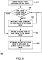
Fig. 6 is a block diagram of an open circuit detection method for the sensor interface and sensor arrangement ofFig. 1 , showing steps of the method. - Reference will now be made to the drawings wherein like reference numerals identify similar structural features or aspects of the subject disclosure. For purposes of explanation and illustration, and not limitation, a partial view of an exemplary embodiment of a sensor interface in accordance with the disclosure is shown in
Fig. 1 and is designated generally byreference character 100. Other embodiments of sensor interfaces, sensor arrangements, and open circuit detection methods in accordance with the disclosure, or aspects thereof, are provided inFigs. 2-6 , as will be described. The systems and methods described herein can be used for open circuit detection in sensor circuits and sensor circuit arrangements for differential voltage sources, such as thermocouples employed for monitoring friction pad temperature in aircraft braking systems, though the present disclosure is not limited to braking systems or to thermocouple differential voltage sources in general. - Referring to
Fig. 1 , asensor arrangement 200 is shown.Sensor arrangement 200 includessensor interface 100 with asensor circuit 102, adifferential voltage source 202, and areadout circuit 204.Readout circuit 204 is connected tosensor circuit 102 and therethrough todifferential voltage source 202. Connection throughsensor circuit 102places readout circuit 204 in electrical communication withdifferential voltage source 202,sensor circuit 102 thereby communicating a differential voltage signal A fromdifferential voltage source 202 toreadout circuit 204. -
Readout circuit 204 is arranged to receive a voltage signal A fromsensor circuit 102. Based on voltage signal A,readout circuit 204 provides an output B to an output lead associated with the magnitude of voltage signal A. Generating output B can include, by way of non-limiting example, amplification via an amplifier (not shown for reasons of clarity). Examples of suitable readout circuits include that described inU.S. Patent No. 4,166, 243 to West et al., issued on August 28, 1979 , the contents of which are incorporated herein by reference in its entirety. -
Differential voltage source 202 is arranged to generate voltage signal A. Voltage signal A can arise, for example, according to change in a device operatively connected todifferential voltage source 202. In certain embodimentsdifferential voltage source 202 can include athermocouple 206.Thermocouple 206 is disposed in thermal communication C with a device ofinterest 10, voltage signal A varying according to change in temperature of device ofinterest 10. Device ofinterest 10 can be a friction pad of landing gear system for anaircraft 12. -
Sensor interface 100 includessensor circuit 102, adiode 104, a back-bias circuit 106 and adrive circuit 108.Diode 104 is arranged to oppose current flow fromsensor circuit 102 to drivecircuit 108, and has ananode 110 and acathode 112.Cathode 112 is connected tosensor circuit 102.Anode 110 is connected to both back-bias circuit 106 and drivecircuit 108 through anintermediate node 116. - A
controller 114 is operably connected to drivecircuit 108.Controller 114 and is arranged to cause drive circuit to apply a test voltage tosensor circuit 102 for open detection.Controller 114 is also disposed in communication withreadout circuit 204 to monitor the affect the test voltage on readout circuit output B,controller 114 thereby determining whethersensor circuit 102 is open. In thisrespect controller 114 is arranged to toggle drive circuit between an active state (shown inFig. 3 ), wherein drive circuit applies adrive voltage 138 todiode 104 sufficient to forwardbias diode 104 andtest sensor circuit 102 for an open circuit condition, and an inactive state (shown inFig. 4 ), wherein an intervening switch 124 (shown inFig. 2 ) is toggled to an off-state to remove thedrive voltage 138 fromdiode 104. Examples of suitable open detection controllers include those described inU.S. Patent No. 8,274,238 to Szczeszynski et al., issued on September 25, 2012 , the contents of which is incorporated herein by reference in its entirety. - As will be appreciated by those of skill in art, open detection functionality can provide indication of whether voltage signal A is reliably indicative of the condition of device of
interest 10. This can be important is certain types of differential voltage sources, such as thermocouples, where voltage output by a differential voltage source when open can be within the expected range of output voltages of the differential voltage source. - As will also be appreciated by those of skill in the art in view of the present disclosure, some open detection circuits can leak current into the monitored sensor circuit. Such leakage currents can alter the magnitude of voltage signal generated by the differential voltage source connected to the sensor circuit. Although such leakage currents generally do not alter the differential voltage source output voltage signal significantly, the leakage current can consume a relatively large portion of the error budge in certain sensor arrangements, rendering incorporation of open circuit detection impossible for certain types of sensor arrangements. As a countermeasure to excessive inactive state current leakage flow, e.g., leakage current flow i (shown in
Fig. 4 ),sensor interface 100 includes back-bias circuit 106. - Back-
bias circuit 106 is connected betweendrive circuit 108 andsensor circuit 102. More particularly, back-bias circuit 106 is connected to anode 110 at 110 through anintermediate node 116 and is arranged to accept leakage current fromdrive circuit 108 throughintermediate node 116 whendrive circuit 108 is in the inactive state (shown inFig. 4 ). Back-bias circuiting current flow fromdrive circuit 108 into back-bias circuit 106 whendrive circuit 108 is in the inactive state prevents substantially all leakage current fromdrive circuit 108 from reachingsensor circuit 102, improving accuracy ofsensor circuit 102 whendrive circuit 108 is inactive. - With reference to
Fig. 2 ,sensor interface 100 is shown.Sensor circuit 102 includes a low-side lead 118 and a high-side lead 120.Differential voltage source 202 is connected in series between low-side lead 118 and high-side lead 120. In the illustrated exemplary embodimentsdifferential voltage source 202 is indicated as a thermocouple. This is for illustration purposes only and is non-limiting.Diode 104 is connected to high-side lead 120. More particularlycathode 112 ofdiode 104 is connected to high-side lead for detection an open circuit, e.g.,open circuit 16, insensor circuit 102. -
Drive circuit 108 includes adrive voltage source 122 and aswitch 124.Drive voltage source 122 is arranged to apply adrive voltage 138 tointermediate node 116 when connected thereto byswitch 124 for applying voltage fromdrive circuit 108 tosensor circuit 102 whendrive circuit 108 is in the active state (shown inFig. 3 ). - Switch 124 can include one or more solid-
state switch device 126. Solid-state switch device 126 can be an NMOS-type or a PMOS type solid-state switch device and has agate 128, asource 130, and adrain 132.Drain 132 is connected tointermediate node 116, and therethrough to anode 110 ofdiode 104 and to back-bias circuit 106.Source 130 is connected to drivevoltage source 122.Gate 128 is connected to controller 114 (shown inFig. 1 ) and receives therethrough command signals D. - Solid-
state switch device 126 is arranged such that command signals D toggles solid-state switch device 126 between an on-state and an off-state. In the on-state, solid-state switch device 126 connectsdrive voltage source 122 to high-side lead 120. This places placingdrive circuit 108 in the active state (shown inFig. 3 ). In the off-state, solid-state switch device 126 applies an off-state resistance 134 to drivecircuit 108. Application of off-state resistance 134 to drivecircuit 108 places drive circuit in the inactive state (shown inFig. 4 ). - Back-
bias circuit 106 includes a back-bias circuit 140 arranged to back-bias circuit current flow fromdrive circuit 108 into back-bias circuit 106 whendrive circuit 108 is in the inactive state (shown inFig. 4 ). In this respect back-bias circuit 106 includes a back-bias resistor 142 and a back-bias voltage source 144. Back-bias resistor 142 is connected todiode 104. More particularly, back-bias resistor 142 is connected inintermediate node 116, and therethrough to both theanode 110 ofdiode 104 and thedrain 132 of solid-state switch device 126. It is contemplated that back-bias resistor 142 have an electrical resistance that is less than or equal to the electrical resistance ofdrive circuit 108 when in the inactive state (shown inFig. 4 ). In certain embodiments, the electrical resistance of back-bias resistor 142 is less than or equal to the electrical resistance of solid-state switch device 126 in the off-state, i.e., is less than or equal to off-state resistance 134. - Back-
bias voltage source 144 is connected to back-bias resistor 142. More particularly, back-bias voltage source 144 is connected to back-bias resistor 142, and therethrough tointermediate node 116, and thereby to bothanode 110 ofdiode 104 and drain 132 of solid-state switch device 126. It is contemplated that back-bias voltage source 144 have a negative back-bias voltage 146. Back-bias voltage 146 is less thandrive voltage 138, less meaning that the magnitude (i.e. absolute value) of back-bias voltage 146 is larger than the magnitude ofdrive voltage 138. In cooperation with the relative resistances of back-bias resistor 142 and off-state resistance 134 of solid-state switch device 126, negative voltage causes leakage current flowing through the body diode of solid-state switch device 126 to flow to back-bias voltage source 144, back-biasingdiode 104, and preventing voltage associated with the leakage from forward biasing diode 104 - isolating the leakage current fromsensor circuit 102. - With reference to
Figs. 3 and4 ,sensor interface 100 is shown in an active state, shown inFig. 3 , and in an inactive state (shown inFig. 4 ). In the activestate drive circuit 108 applies voltage sufficient to forwardbias diode 104, allowing a current flow I to traversediode 104. It is contemplated that current flow I be off-scale, meaning the resultant differential voltage signal A (shown inFig. 1 ) is outside the range of differential output voltages from differential voltage source 202 (shown inFig. 1 ). - In the inactive state (shown in
Fig. 4 ) back-bias circuit 106 attenuates leakage current i flowing throughdiode 104. It is contemplated that back-bias circuit 106 limit leakage current flow i such that the associated voltage is insufficient toforward bias diode 104, current flowingdiode 104 having very little (if any) impact on the accuracy of differential voltage signal A (shown inFig. 1 ). - Referring now to
Fig. 5 , a table 300 of exemplary leakage current flows is shown for conditions 1-5 ofsensor interface 100. Table 300 shows leakage current flow i throughdiode 104 as a function of back-bias voltage 146 of back-bias voltage source 144, resistance of back-bias resistor 142, off-state state resistance 134 ofdrive circuit 108, and drivevoltage 138. Notably, in conditions 2-4 voltage applied to anode 110 ofdiode 104 was found to be insufficient toforward bias diode 104, resulting in leakage current flow i of magnitude insufficient to degrade differential voltage signal A (shown inFig. 1 ). - As shown in the first row of table 300, when back-
bias resistor 142 has infinite resistance leakage current i throughdiode 104 am about 4.5 micro-amps, which can consume an unacceptable portion of the error budget in some sensor arrangement. - The second row of table 300 shows a first exemplary implementation of sensor interface 100 (shown in
Fig. 1 ). Notably, when a back bias circuit is connected to anode 110 ofdiode 104 with a back-bias resistance of 1 mega-ohm and a back-bias voltage of-5 volts, and an open-detectvoltage of+ 5 volts applied through a switch with an off-state resistance of 1 mega-ohm, the resulting voltage atanode 110 drops from the 440 millivolts exhibited incondition 1 to - 5 volts. Since -5 volts is insufficient toforward bias diode 104, leakage current incondition 2 drops to about -0.2 micro-amps. Leakage currents in this range are acceptable insofar as the accuracy impact to sensor arrangement 200 (shown inFig. 1 ) is more than offset by the advantages of the added open circuit detection capability provided bydrive circuit 108. - The third row of table 300 shows an implementation of
sensor interface 100 where in the inactive-state resistance ofdrive circuit 108 is increased to 10 mega-ohms in comparison tocondition 2. This causes the voltage applied to anode 110 ofdiode 104 to further drop. Notably, leakage current i remain substantially equivalent to that ofcondition 2, indicating the added expense of selecting a solid-state switch device with increased off-state resistance brings little additional benefit for the added expense. - The fourth row of table 300 shows an implementation of
sensor interface 100 where in the inactive-state resistance ofdrive circuit 108 is decreased to 0.5 mega-ohms in comparison tocondition 2. This causes the voltage applied to anode 110 ofdiode 104 to increase to about -1.6 volts. Notably, leakage current i remain substantially equivalent to that ofconditions forward bias diode 104. This suggests that it may be possible to select aswitch 124 with lower off-state resistance, which can potentially reduce the cost ofdrive circuit 108. - The fifth row of table 300 indicates that there is a point where further reduction in the off-state resistance of
switch 124 begins to drive leakage current i to unacceptable levels notwithstanding the advantageous effect of back-biasingdiode 104. Notably, when the off-state resistance ofswitch 124 drops to 0.1 mega-ohms voltage applied to anode 110 ofdiode 104 rises to 0.7 volts - which is sufficient to forward bias diode 104 - and results in a leakage current of 27 micro-amps, which can consume an unacceptable portion of the error budget ofsensor arrangement 200. - With reference to
Fig. 6 , an opencircuit detection method 400 for a sensor interface, e.g., sensor interface 100 (shown inFig. 1 ), is shown.Method 400 includes monitoring voltage from a differential voltage source, e.g., differential voltage source 202 (shown inFig. 1 ), as shown withbox 410. During monitoring the drive circuit is determined to either be in an active state (shown inFig. 3 ) or an inactive state (shown inFig. 4 ), as shown withbox 420. When the circuit is in the inactive state a diode, e.g., diode 104 (shown inFig. 1 ), is back-biased, as show withbox 430. When the circuit is in the active state a voltage from a drive circuit, e.g.,drive circuit 108, is applied to the sensor circuit, as shown withbox 440. Based on resultant current flow in the sensor circuit a determination is made as to whether the sensor circuit is open or closed, as shown withbox 450. - Direct current (DC) off-scale drive circuitry can be used to detect open conditions in sensing circuits, e.g., sensor circuit 102 (shown in
Fig. 1 ). In some sensor circuits, such as in high accuracy low level applications, DC off-scale drive circuitry can consume relatively large portions of the required accuracy band of the sensor communicative with the sensing circuit. In certain applications the impact of open circuit monitoring using DC off-scale drive circuitry can increase the sensor error by 1.65% or more, which can exceed the error budget in some application. - One approach to the problem open monitoring inducing error in sensor circuit output is the use of a switched open monitoring circuit. Switched open circuit monitoring circuits employ a switched DC off-scale driver circuits, e.g., drive circuit 108 (shown in
Fig. 1 ). Such switched DC off-scale driver circuits can generally reduce the accuracy penalty associated with open condition monitoring to increases in sensor error on the order of about 0.8%. While generally satisfactory for its intended purpose, errors of this side can still be prohibitive in some applications, thermocouples used for temperature sensing in aircraft brake systems, where errors of 0.8% can drive temperature accuracy errors of 3 degrees Celsius or more, potentially making open circuit monitoring prohibitive in such applications. - In embodiments described herein DC off-scale drive circuitry for open condition monitoring is supplemented a back-biased diode, e.g., diode 104 (shown in
Fig. 1 ). The back-biased diode is connected to a drive voltage source, e.g., drive voltage source 122 (shown inFig. 2 ), for checking for open condition of the sensor circuit by applying a positive voltage to the anode. In certain embodiments, back-biasing of the diode by a back-bias circuit, e.g., back-bias circuit 106, allows only a very small amount of leakage current to reach the sensing circuit by limiting the forward bias voltage applied to the diode. This prevents the open circuit monitoring circuitry from reducing the accuracy of the measurement information conveyed by the differential voltage signal carried by the sensing circuit. Applicant's demonstration experimentation with the circuit arrangement has shown that the error associated with open condition monitoring can be restricted by 0.01% or less with the use of a back-bias circuit, e.g., back-bias circuit 106 (shown inFig. 1 ), incorporating the back-biased diode. - The methods and systems of the present disclosure, as described above and shown in the drawings, provide for open detectors and methods of detecting open circuits with superior properties including reduced current leakage from the detection circuit to the monitored circuit through the use of a back-biased diode. In certain embodiments a resistor with resistance that is slightly less than the on-resistance of the switch connecting the diode to the voltage source is also employed to further reduce leakage from the detection circuit to the monitored circuit. While the apparatus and methods of the subject disclosure have been shown and described with reference to preferred embodiments, those skilled in the art will readily appreciate that changes and/or modifications may be made thereto without departing from the scope of the subject disclosure.
Claims (15)
- A sensor interface (100), comprising:a sensor circuit (102);a drive circuit (108) connected to the sensor circuit with active and inactive states; anda back-bias circuit (106) connected between the drive circuit (108) and the sensor circuit (102),wherein the back-bias circuit (106) is arranged to allow current to flow from the drive circuit (108) to the sensor circuit (102) when the drive circuit (108) is in the active state, andwherein the back-bias circuit (106) is arranged to limit current flow from the drive circuit (108) to the sensor circuit (102) when the drive circuit (108) is in the inactive state.
- The sensor interface as recited in claim 1, further comprising a diode (104) connecting the drive circuit (108) to the sensor circuit (102), the diode (104) arranged to oppose current flow from the sensor circuit (102) to the drive circuit (108).
- The sensor interface as recited in claim 2, wherein back-bias circuit (106) includes a back-bias resistor (142), the back-bias resistor (142) connected to the diode, and preferably wherein the back-bias resistor (142) has electrical resistance that is less than or equal to resistance of the drive circuit (102) when in the inactive state.
- The sensor interface as recited in claim 2, wherein the back-bias circuit (106) includes a back-bias voltage source (144), a back-bias resistor (142) of the back-bias circuit (106) connecting the back-bias voltage source (144) to the diode (104), and preferably wherein the drive circuit (102) includes a drive voltage source, the drive circuit connecting the drive voltage source to the diode (104), wherein the back-bias voltage source is less than the drive voltage source.
- The sensor interface as recited in any preceding claim, wherein the drive circuit (108) includes a switch, the switch connecting the drive circuit to the sensor circuit (102).
- The sensor interface as recited in claim 5, wherein the switch has off-state resistance greater than or equal to resistance of the back-bias circuit, and/or wherein the drive circuit includes a drive voltage source, the switch connecting the drive voltage source to the sensor circuit, and/or wherein the switch includes a solid-state switch device with a gate, and further comprising a controller operatively connected to the gate of the solid-state switch device.
- The sensor interface as recited in any preceding claim, wherein the sensor circuit (102) includes a high-side lead and a low-side lead, the back-bias circuit (106) and the drive circuit (102) both connected to the high-side lead, and preferably further comprising a differential voltage source connected in series between the high-side lead and the low-side lead.
- The sensor interface as recited in claim 7, further comprising a thermocouple connected in series between the high-side lead and the low-side lead.
- A sensor arrangement (200), comprising:a sensor interface (100) as recited in any preceding claim, wherein the sensor circuit (102) includes a high-side lead and a low-side lead, the back-bias circuit connected to the high-side lead;a differential voltage source connected in series between the high-side lead and the low-side lead of the sensor circuit;a diode (104) connected to the sensor circuit and arranged oppose current flow from the sensor circuit to the drive circuit (108),wherein the drive circuit (108) includes a switch, the switch connecting the drive circuit (108) to the diode (104), and wherein the back-bias circuit (106) is connected to the diode (104) and has resistance that is less than or equal to resistance of the drive circuit (108) in the inactive state.
- The sensor arrangement as recited in claim 9, wherein the back-bias circuit (106) includes a back-bias voltage source (144), the back-bias voltage source (144) connected to the diode (104), wherein the drive circuit (108) includes a drive voltage source, the drive voltage source connected to the diode (104), wherein voltage of the back-bias voltage source (144) is lower than voltage of the drive voltage source.
- The sensor arrangement as recited in claim 9 or 10, wherein magnitude of the back-bias voltage source is greater than magnitude of the drive voltage source.
- The sensor arrangement as recited in any of claims 9 to 11, wherein the back-bias circuit (106) includes a back-bias resistor (142), the back-bias resistor (142) connected to the diode (104), wherein the back-bias resistor (142) has resistance that is less than or equal to resistance of the drive circuit (108) in the inactive state.
- The sensor arrangement as recited in any of claims 9 to 12, wherein the differential voltage source (202) includes a thermocouple.
- The sensor arrangement as recited in any of claims 9 to 13, further comprising a brake friction pad in thermal communication with the differential voltage source.
- An open circuit detection method, comprising:at a sensor interface (100) having a sensor circuit (102), a drive circuit (108) connected to the sensor circuit (102) with active and inactive states, and a back-bias circuit connected between the drive circuit (108) and the sensor circuit (102),applying voltage from the drive circuit (108) to the sensor circuit (102) when the drive circuit (108) is in the active state; anddetermining whether the sensor circuit (102) is open based on current flow from the drive circuit to the sensor circuit when the drive circuit is in the active state; andback-biasing a diode (104) connecting the drive circuit (102) to the sensor interface when the drive circuit is in the inactive state to limit current flow to the sensor interface (100) when the drive circuit (108) is in the inactive state.
Applications Claiming Priority (1)
| Application Number | Priority Date | Filing Date | Title |
|---|---|---|---|
| US15/727,356 US10732231B2 (en) | 2017-10-06 | 2017-10-06 | Sensor interfaces, sensor arrangements, and open circuit detection methods for sensor interfaces and arrangements |
Publications (2)
| Publication Number | Publication Date |
|---|---|
| EP3467524A1 true EP3467524A1 (en) | 2019-04-10 |
| EP3467524B1 EP3467524B1 (en) | 2020-07-01 |
Family
ID=63794370
Family Applications (1)
| Application Number | Title | Priority Date | Filing Date |
|---|---|---|---|
| EP18199088.8A Active EP3467524B1 (en) | 2017-10-06 | 2018-10-08 | Sensor interfaces, sensor arrangements, and open circuit detection methods for sensor interfaces and arrangements |
Country Status (2)
| Country | Link |
|---|---|
| US (1) | US10732231B2 (en) |
| EP (1) | EP3467524B1 (en) |
Families Citing this family (1)
| Publication number | Priority date | Publication date | Assignee | Title |
|---|---|---|---|---|
| US11852662B2 (en) | 2021-10-20 | 2023-12-26 | Hamilton Sundstrand Corporation | Open-wire detection for analog differential inputs using an alternating current (AC) bias |
Citations (7)
| Publication number | Priority date | Publication date | Assignee | Title |
|---|---|---|---|---|
| US3944288A (en) * | 1974-02-04 | 1976-03-16 | Kelsey-Hayes Company | Skid control system for two-wheeled vehicles |
| US4143926A (en) * | 1977-01-27 | 1979-03-13 | Kelsey-Hayes Co. | Skid control system |
| US4166243A (en) | 1978-04-21 | 1979-08-28 | General Motors Corporation | Thermocouple failure detector |
| US5352938A (en) * | 1992-12-14 | 1994-10-04 | Delco Electronics Corporation | Analog to digital signal conversion |
| US20010035723A1 (en) * | 2000-02-23 | 2001-11-01 | Pelrine Ronald E. | Biologically powered electroactive polymer generators |
| US8274238B2 (en) | 2007-01-04 | 2012-09-25 | Allegro Microsystems, Inc. | Electronic circuit for driving a diode load |
| CN105686884A (en) * | 2016-01-07 | 2016-06-22 | 邱彦明 | An intelligent temperature protection device |
Family Cites Families (3)
| Publication number | Priority date | Publication date | Assignee | Title |
|---|---|---|---|---|
| US7626344B2 (en) * | 2007-08-03 | 2009-12-01 | Osram Sylvania Inc. | Programmed ballast with resonant inverter and method for discharge lamps |
| CN103427395B (en) | 2012-05-21 | 2017-03-01 | 台达电子工业股份有限公司 | Open circuit protection circuit, open circuit protection method and lighting device |
| JP6469481B2 (en) | 2015-03-03 | 2019-02-13 | ローム株式会社 | Insulation synchronous rectification type DC / DC converter, secondary side controller, power supply device using the same, power supply adapter, and electronic equipment |
-
2017
- 2017-10-06 US US15/727,356 patent/US10732231B2/en active Active
-
2018
- 2018-10-08 EP EP18199088.8A patent/EP3467524B1/en active Active
Patent Citations (7)
| Publication number | Priority date | Publication date | Assignee | Title |
|---|---|---|---|---|
| US3944288A (en) * | 1974-02-04 | 1976-03-16 | Kelsey-Hayes Company | Skid control system for two-wheeled vehicles |
| US4143926A (en) * | 1977-01-27 | 1979-03-13 | Kelsey-Hayes Co. | Skid control system |
| US4166243A (en) | 1978-04-21 | 1979-08-28 | General Motors Corporation | Thermocouple failure detector |
| US5352938A (en) * | 1992-12-14 | 1994-10-04 | Delco Electronics Corporation | Analog to digital signal conversion |
| US20010035723A1 (en) * | 2000-02-23 | 2001-11-01 | Pelrine Ronald E. | Biologically powered electroactive polymer generators |
| US8274238B2 (en) | 2007-01-04 | 2012-09-25 | Allegro Microsystems, Inc. | Electronic circuit for driving a diode load |
| CN105686884A (en) * | 2016-01-07 | 2016-06-22 | 邱彦明 | An intelligent temperature protection device |
Also Published As
| Publication number | Publication date |
|---|---|
| US20190107571A1 (en) | 2019-04-11 |
| US10732231B2 (en) | 2020-08-04 |
| EP3467524B1 (en) | 2020-07-01 |
Similar Documents
| Publication | Publication Date | Title |
|---|---|---|
| EP2467939B1 (en) | Detection and compensation of multiplexer leakage current | |
| EP3049779B1 (en) | Method and apparatus for determining an actual junction temperature of an igbt device | |
| US9726705B2 (en) | Sensor interface circuits | |
| EP2609408B1 (en) | Process fluid temperature measurement | |
| US9772369B2 (en) | Precision measurement of voltage drop across a semiconductor switching element | |
| CN107436407B (en) | Measurements in Switching Devices | |
| CN104583787A (en) | Devices for diagnosing circuit assemblies | |
| KR100838751B1 (en) | How to diagnose the condition of burn-in device | |
| EP2760093B1 (en) | Power switch fault detection system | |
| EP3467524B1 (en) | Sensor interfaces, sensor arrangements, and open circuit detection methods for sensor interfaces and arrangements | |
| US10371735B2 (en) | Method and system for monitoring electrical isolation | |
| CN115622372A (en) | Driver device for NMOS power transistors and blocking circuits in stress test mode | |
| EP3348977B1 (en) | Failure tolerant thermovoltage acquisition for thermocouple applications | |
| EP4096349B1 (en) | Positive temperature coefficient resistor heater assembly health monitoring | |
| JP5319982B2 (en) | Semiconductor device | |
| KR20060050363A (en) | Shunt detection method in sensor | |
| US10393597B2 (en) | Over-temperature detector with test mode | |
| KR101499988B1 (en) | How to diagnose the trouble of cooling fan for hybrid vehicle | |
| CN109792148B (en) | Protective circuit | |
| US10585135B2 (en) | Built in test of remote isolation | |
| EP3719463B1 (en) | Highly failure tolerant temperature acquisition for thermocouple applications | |
| CN118914668A (en) | Device and method for measuring contact resistance | |
| Odungide | Self-Validating Sensors, Types and Uncertainty: A Literature Review | |
| JPS63173976A (en) | Semiconductor test head apparatus | |
| US20120038407A1 (en) | Circuit Arrangement and Input Assembly |
Legal Events
| Date | Code | Title | Description |
|---|---|---|---|
| PUAI | Public reference made under article 153(3) epc to a published international application that has entered the european phase |
Free format text: ORIGINAL CODE: 0009012 |
|
| STAA | Information on the status of an ep patent application or granted ep patent |
Free format text: STATUS: THE APPLICATION HAS BEEN PUBLISHED |
|
| AK | Designated contracting states |
Kind code of ref document: A1 Designated state(s): AL AT BE BG CH CY CZ DE DK EE ES FI FR GB GR HR HU IE IS IT LI LT LU LV MC MK MT NL NO PL PT RO RS SE SI SK SM TR |
|
| AX | Request for extension of the european patent |
Extension state: BA ME |
|
| STAA | Information on the status of an ep patent application or granted ep patent |
Free format text: STATUS: REQUEST FOR EXAMINATION WAS MADE |
|
| 17P | Request for examination filed |
Effective date: 20191008 |
|
| RBV | Designated contracting states (corrected) |
Designated state(s): AL AT BE BG CH CY CZ DE DK EE ES FI FR GB GR HR HU IE IS IT LI LT LU LV MC MK MT NL NO PL PT RO RS SE SI SK SM TR |
|
| RIC1 | Information provided on ipc code assigned before grant |
Ipc: G01R 31/28 20060101AFI20191126BHEP Ipc: G01R 31/02 20060101ALI20191126BHEP |
|
| GRAP | Despatch of communication of intention to grant a patent |
Free format text: ORIGINAL CODE: EPIDOSNIGR1 |
|
| STAA | Information on the status of an ep patent application or granted ep patent |
Free format text: STATUS: GRANT OF PATENT IS INTENDED |
|
| INTG | Intention to grant announced |
Effective date: 20200108 |
|
| GRAS | Grant fee paid |
Free format text: ORIGINAL CODE: EPIDOSNIGR3 |
|
| GRAA | (expected) grant |
Free format text: ORIGINAL CODE: 0009210 |
|
| STAA | Information on the status of an ep patent application or granted ep patent |
Free format text: STATUS: THE PATENT HAS BEEN GRANTED |
|
| AK | Designated contracting states |
Kind code of ref document: B1 Designated state(s): AL AT BE BG CH CY CZ DE DK EE ES FI FR GB GR HR HU IE IS IT LI LT LU LV MC MK MT NL NO PL PT RO RS SE SI SK SM TR |
|
| REG | Reference to a national code |
Ref country code: CH Ref legal event code: EP Ref country code: AT Ref legal event code: REF Ref document number: 1286663 Country of ref document: AT Kind code of ref document: T Effective date: 20200715 |
|
| REG | Reference to a national code |
Ref country code: IE Ref legal event code: FG4D |
|
| REG | Reference to a national code |
Ref country code: DE Ref legal event code: R096 Ref document number: 602018005700 Country of ref document: DE |
|
| REG | Reference to a national code |
Ref country code: LT Ref legal event code: MG4D |
|
| PG25 | Lapsed in a contracting state [announced via postgrant information from national office to epo] |
Ref country code: BG Free format text: LAPSE BECAUSE OF FAILURE TO SUBMIT A TRANSLATION OF THE DESCRIPTION OR TO PAY THE FEE WITHIN THE PRESCRIBED TIME-LIMIT Effective date: 20201001 |
|
| REG | Reference to a national code |
Ref country code: NL Ref legal event code: MP Effective date: 20200701 |
|
| REG | Reference to a national code |
Ref country code: AT Ref legal event code: MK05 Ref document number: 1286663 Country of ref document: AT Kind code of ref document: T Effective date: 20200701 |
|
| PG25 | Lapsed in a contracting state [announced via postgrant information from national office to epo] |
Ref country code: FI Free format text: LAPSE BECAUSE OF FAILURE TO SUBMIT A TRANSLATION OF THE DESCRIPTION OR TO PAY THE FEE WITHIN THE PRESCRIBED TIME-LIMIT Effective date: 20200701 Ref country code: LT Free format text: LAPSE BECAUSE OF FAILURE TO SUBMIT A TRANSLATION OF THE DESCRIPTION OR TO PAY THE FEE WITHIN THE PRESCRIBED TIME-LIMIT Effective date: 20200701 Ref country code: CZ Free format text: LAPSE BECAUSE OF FAILURE TO SUBMIT A TRANSLATION OF THE DESCRIPTION OR TO PAY THE FEE WITHIN THE PRESCRIBED TIME-LIMIT Effective date: 20200701 Ref country code: AT Free format text: LAPSE BECAUSE OF FAILURE TO SUBMIT A TRANSLATION OF THE DESCRIPTION OR TO PAY THE FEE WITHIN THE PRESCRIBED TIME-LIMIT Effective date: 20200701 Ref country code: PT Free format text: LAPSE BECAUSE OF FAILURE TO SUBMIT A TRANSLATION OF THE DESCRIPTION OR TO PAY THE FEE WITHIN THE PRESCRIBED TIME-LIMIT Effective date: 20201102 Ref country code: NO Free format text: LAPSE BECAUSE OF FAILURE TO SUBMIT A TRANSLATION OF THE DESCRIPTION OR TO PAY THE FEE WITHIN THE PRESCRIBED TIME-LIMIT Effective date: 20201001 Ref country code: GR Free format text: LAPSE BECAUSE OF FAILURE TO SUBMIT A TRANSLATION OF THE DESCRIPTION OR TO PAY THE FEE WITHIN THE PRESCRIBED TIME-LIMIT Effective date: 20201002 Ref country code: ES Free format text: LAPSE BECAUSE OF FAILURE TO SUBMIT A TRANSLATION OF THE DESCRIPTION OR TO PAY THE FEE WITHIN THE PRESCRIBED TIME-LIMIT Effective date: 20200701 Ref country code: HR Free format text: LAPSE BECAUSE OF FAILURE TO SUBMIT A TRANSLATION OF THE DESCRIPTION OR TO PAY THE FEE WITHIN THE PRESCRIBED TIME-LIMIT Effective date: 20200701 Ref country code: SE Free format text: LAPSE BECAUSE OF FAILURE TO SUBMIT A TRANSLATION OF THE DESCRIPTION OR TO PAY THE FEE WITHIN THE PRESCRIBED TIME-LIMIT Effective date: 20200701 |
|
| PG25 | Lapsed in a contracting state [announced via postgrant information from national office to epo] |
Ref country code: RS Free format text: LAPSE BECAUSE OF FAILURE TO SUBMIT A TRANSLATION OF THE DESCRIPTION OR TO PAY THE FEE WITHIN THE PRESCRIBED TIME-LIMIT Effective date: 20200701 Ref country code: PL Free format text: LAPSE BECAUSE OF FAILURE TO SUBMIT A TRANSLATION OF THE DESCRIPTION OR TO PAY THE FEE WITHIN THE PRESCRIBED TIME-LIMIT Effective date: 20200701 Ref country code: LV Free format text: LAPSE BECAUSE OF FAILURE TO SUBMIT A TRANSLATION OF THE DESCRIPTION OR TO PAY THE FEE WITHIN THE PRESCRIBED TIME-LIMIT Effective date: 20200701 Ref country code: IS Free format text: LAPSE BECAUSE OF FAILURE TO SUBMIT A TRANSLATION OF THE DESCRIPTION OR TO PAY THE FEE WITHIN THE PRESCRIBED TIME-LIMIT Effective date: 20201101 |
|
| PG25 | Lapsed in a contracting state [announced via postgrant information from national office to epo] |
Ref country code: NL Free format text: LAPSE BECAUSE OF FAILURE TO SUBMIT A TRANSLATION OF THE DESCRIPTION OR TO PAY THE FEE WITHIN THE PRESCRIBED TIME-LIMIT Effective date: 20200701 |
|
| REG | Reference to a national code |
Ref country code: DE Ref legal event code: R097 Ref document number: 602018005700 Country of ref document: DE |
|
| PG25 | Lapsed in a contracting state [announced via postgrant information from national office to epo] |
Ref country code: SM Free format text: LAPSE BECAUSE OF FAILURE TO SUBMIT A TRANSLATION OF THE DESCRIPTION OR TO PAY THE FEE WITHIN THE PRESCRIBED TIME-LIMIT Effective date: 20200701 Ref country code: IT Free format text: LAPSE BECAUSE OF FAILURE TO SUBMIT A TRANSLATION OF THE DESCRIPTION OR TO PAY THE FEE WITHIN THE PRESCRIBED TIME-LIMIT Effective date: 20200701 Ref country code: EE Free format text: LAPSE BECAUSE OF FAILURE TO SUBMIT A TRANSLATION OF THE DESCRIPTION OR TO PAY THE FEE WITHIN THE PRESCRIBED TIME-LIMIT Effective date: 20200701 Ref country code: RO Free format text: LAPSE BECAUSE OF FAILURE TO SUBMIT A TRANSLATION OF THE DESCRIPTION OR TO PAY THE FEE WITHIN THE PRESCRIBED TIME-LIMIT Effective date: 20200701 Ref country code: DK Free format text: LAPSE BECAUSE OF FAILURE TO SUBMIT A TRANSLATION OF THE DESCRIPTION OR TO PAY THE FEE WITHIN THE PRESCRIBED TIME-LIMIT Effective date: 20200701 |
|
| PLBE | No opposition filed within time limit |
Free format text: ORIGINAL CODE: 0009261 |
|
| STAA | Information on the status of an ep patent application or granted ep patent |
Free format text: STATUS: NO OPPOSITION FILED WITHIN TIME LIMIT |
|
| PG25 | Lapsed in a contracting state [announced via postgrant information from national office to epo] |
Ref country code: AL Free format text: LAPSE BECAUSE OF FAILURE TO SUBMIT A TRANSLATION OF THE DESCRIPTION OR TO PAY THE FEE WITHIN THE PRESCRIBED TIME-LIMIT Effective date: 20200701 |
|
| 26N | No opposition filed |
Effective date: 20210406 |
|
| PG25 | Lapsed in a contracting state [announced via postgrant information from national office to epo] |
Ref country code: SK Free format text: LAPSE BECAUSE OF FAILURE TO SUBMIT A TRANSLATION OF THE DESCRIPTION OR TO PAY THE FEE WITHIN THE PRESCRIBED TIME-LIMIT Effective date: 20200701 Ref country code: LU Free format text: LAPSE BECAUSE OF NON-PAYMENT OF DUE FEES Effective date: 20201008 Ref country code: MC Free format text: LAPSE BECAUSE OF FAILURE TO SUBMIT A TRANSLATION OF THE DESCRIPTION OR TO PAY THE FEE WITHIN THE PRESCRIBED TIME-LIMIT Effective date: 20200701 |
|
| REG | Reference to a national code |
Ref country code: BE Ref legal event code: MM Effective date: 20201031 |
|
| PG25 | Lapsed in a contracting state [announced via postgrant information from national office to epo] |
Ref country code: BE Free format text: LAPSE BECAUSE OF NON-PAYMENT OF DUE FEES Effective date: 20201031 Ref country code: SI Free format text: LAPSE BECAUSE OF FAILURE TO SUBMIT A TRANSLATION OF THE DESCRIPTION OR TO PAY THE FEE WITHIN THE PRESCRIBED TIME-LIMIT Effective date: 20200701 |
|
| PG25 | Lapsed in a contracting state [announced via postgrant information from national office to epo] |
Ref country code: IE Free format text: LAPSE BECAUSE OF NON-PAYMENT OF DUE FEES Effective date: 20201008 |
|
| REG | Reference to a national code |
Ref country code: CH Ref legal event code: PL |
|
| PG25 | Lapsed in a contracting state [announced via postgrant information from national office to epo] |
Ref country code: TR Free format text: LAPSE BECAUSE OF FAILURE TO SUBMIT A TRANSLATION OF THE DESCRIPTION OR TO PAY THE FEE WITHIN THE PRESCRIBED TIME-LIMIT Effective date: 20200701 Ref country code: MT Free format text: LAPSE BECAUSE OF FAILURE TO SUBMIT A TRANSLATION OF THE DESCRIPTION OR TO PAY THE FEE WITHIN THE PRESCRIBED TIME-LIMIT Effective date: 20200701 Ref country code: CY Free format text: LAPSE BECAUSE OF FAILURE TO SUBMIT A TRANSLATION OF THE DESCRIPTION OR TO PAY THE FEE WITHIN THE PRESCRIBED TIME-LIMIT Effective date: 20200701 |
|
| PG25 | Lapsed in a contracting state [announced via postgrant information from national office to epo] |
Ref country code: MK Free format text: LAPSE BECAUSE OF FAILURE TO SUBMIT A TRANSLATION OF THE DESCRIPTION OR TO PAY THE FEE WITHIN THE PRESCRIBED TIME-LIMIT Effective date: 20200701 |
|
| PG25 | Lapsed in a contracting state [announced via postgrant information from national office to epo] |
Ref country code: LI Free format text: LAPSE BECAUSE OF NON-PAYMENT OF DUE FEES Effective date: 20211031 Ref country code: CH Free format text: LAPSE BECAUSE OF NON-PAYMENT OF DUE FEES Effective date: 20211031 |
|
| P01 | Opt-out of the competence of the unified patent court (upc) registered |
Effective date: 20230522 |
|
| PGFP | Annual fee paid to national office [announced via postgrant information from national office to epo] |
Ref country code: GB Payment date: 20250923 Year of fee payment: 8 |
|
| PGFP | Annual fee paid to national office [announced via postgrant information from national office to epo] |
Ref country code: FR Payment date: 20250924 Year of fee payment: 8 |
|
| PGFP | Annual fee paid to national office [announced via postgrant information from national office to epo] |
Ref country code: DE Payment date: 20250923 Year of fee payment: 8 |