EP3467521A1 - Discrete input determining circuit and method - Google Patents
Discrete input determining circuit and method Download PDFInfo
- Publication number
- EP3467521A1 EP3467521A1 EP18198161.4A EP18198161A EP3467521A1 EP 3467521 A1 EP3467521 A1 EP 3467521A1 EP 18198161 A EP18198161 A EP 18198161A EP 3467521 A1 EP3467521 A1 EP 3467521A1
- Authority
- EP
- European Patent Office
- Prior art keywords
- input
- voltage
- output
- discrete
- input voltage
- Prior art date
- Legal status (The legal status is an assumption and is not a legal conclusion. Google has not performed a legal analysis and makes no representation as to the accuracy of the status listed.)
- Granted
Links
Images

Classifications
-
- G—PHYSICS
- G01—MEASURING; TESTING
- G01R—MEASURING ELECTRIC VARIABLES; MEASURING MAGNETIC VARIABLES
- G01R19/00—Arrangements for measuring currents or voltages or for indicating presence or sign thereof
- G01R19/165—Indicating that current or voltage is either above or below a predetermined value or within or outside a predetermined range of values
- G01R19/16533—Indicating that current or voltage is either above or below a predetermined value or within or outside a predetermined range of values characterised by the application
- G01R19/16557—Logic probes, i.e. circuits indicating logic state (high, low, O)
-
- G—PHYSICS
- G01—MEASURING; TESTING
- G01R—MEASURING ELECTRIC VARIABLES; MEASURING MAGNETIC VARIABLES
- G01R15/00—Details of measuring arrangements of the types provided for in groups G01R17/00 - G01R29/00, G01R33/00 - G01R33/26 or G01R35/00
- G01R15/04—Voltage dividers
-
- G—PHYSICS
- G01—MEASURING; TESTING
- G01R—MEASURING ELECTRIC VARIABLES; MEASURING MAGNETIC VARIABLES
- G01R19/00—Arrangements for measuring currents or voltages or for indicating presence or sign thereof
- G01R19/0038—Circuits for comparing several input signals and for indicating the result of this comparison, e.g. equal, different, greater, smaller (comparing pulses or pulse trains according to amplitude)
-
- G—PHYSICS
- G01—MEASURING; TESTING
- G01R—MEASURING ELECTRIC VARIABLES; MEASURING MAGNETIC VARIABLES
- G01R19/00—Arrangements for measuring currents or voltages or for indicating presence or sign thereof
- G01R19/165—Indicating that current or voltage is either above or below a predetermined value or within or outside a predetermined range of values
- G01R19/16566—Circuits and arrangements for comparing voltage or current with one or several thresholds and for indicating the result not covered by subgroups G01R19/16504, G01R19/16528, G01R19/16533
- G01R19/1659—Circuits and arrangements for comparing voltage or current with one or several thresholds and for indicating the result not covered by subgroups G01R19/16504, G01R19/16528, G01R19/16533 to indicate that the value is within or outside a predetermined range of values (window)
-
- H—ELECTRICITY
- H02—GENERATION; CONVERSION OR DISTRIBUTION OF ELECTRIC POWER
- H02H—EMERGENCY PROTECTIVE CIRCUIT ARRANGEMENTS
- H02H3/00—Emergency protective circuit arrangements for automatic disconnection directly responsive to an undesired change from normal electric working condition with or without subsequent reconnection ; integrated protection
- H02H3/26—Emergency protective circuit arrangements for automatic disconnection directly responsive to an undesired change from normal electric working condition with or without subsequent reconnection ; integrated protection responsive to difference between voltages or between currents; responsive to phase angle between voltages or between currents
- H02H3/32—Emergency protective circuit arrangements for automatic disconnection directly responsive to an undesired change from normal electric working condition with or without subsequent reconnection ; integrated protection responsive to difference between voltages or between currents; responsive to phase angle between voltages or between currents involving comparison of the voltage or current values at corresponding points in different conductors of a single system, e.g. of currents in go and return conductors
-
- G—PHYSICS
- G01—MEASURING; TESTING
- G01R—MEASURING ELECTRIC VARIABLES; MEASURING MAGNETIC VARIABLES
- G01R31/00—Arrangements for testing electric properties; Arrangements for locating electric faults; Arrangements for electrical testing characterised by what is being tested not provided for elsewhere
- G01R31/005—Testing of electric installations on transport means
- G01R31/008—Testing of electric installations on transport means on air- or spacecraft, railway rolling stock or sea-going vessels
Definitions
- This disclosure relates generally to the field of aircraft, and more particularly to a discrete input determining circuit and a discrete input determining method.
- Avionics products often provide circuits to read, ascertain or otherwise determine discrete inputs from other equipment in the aircraft.
- the discrete inputs may conform, for example, to one of two types: OPEN/GND or 28V/OPEN.
- Avionics products have typically used two different circuits to accommodate the two discrete types, providing internal pullups for the OPEN/GND discrete input and internal pulldowns for 28V/OPEN discrete input. Therefore, the avionics products have frequently provided a quantity of each circuit type to cover a variety of possible aircraft applications. For any given application, rarely are all the discrete inputs of both types utilized, and often there is a shortage of one type or the other. This may result in valuable hardware being left unused, reducing the flexibility and cost-effectiveness of the product.
- a discrete input determining circuit comprises an input biasing network connected to a discrete input for providing a first input voltage, a voltage divider network for dividing the first input voltage into a second input voltage and a third input voltage, a first comparator and a second comparator.
- a non-inverting input terminal of the first comparator receives the second input voltage
- an inverting input terminal of the second comparator receives the third input voltage.
- An inverting input terminal of the first comparator and a non-inverting input terminal of the second comparator receive a reference voltage, and an output terminal of the first comparator and an output terminal of the second comparator are configured to provide a logic output.
- a discrete input determining method comprises biasing the discrete input to provide a first input voltage, dividing the first input voltage into a second input voltage and a third input voltage, comparing the second input with a reference voltage and outputting a first output, comparing the reference voltage with the third input and outputting a second output, and outputting a logic output by a logic function between the first output and the second output.
- connection and “coupled” are not restricted to physical or mechanical connections or couplings, and can include electrical connections or couplings, whether direct or indirect.
- Terms indicating specific locations such as “top”, “bottom”, “left”, and “right”, are descriptions with reference to specific accompanying drawings. Embodiments disclosed in the present disclosure may be placed in a manner different from that shown in the figures. Therefore, the location terms used herein should not be limited to locations described in specific embodiments.
- FIG. 1 illustrates a schematic diagram of a discrete input determining circuit 100.
- the discrete input determining circuit 100 comprises an input biasing network 110 connected to a discrete input for providing a first input voltage V 1 , a voltage divider network 120 for dividing the first input voltage V 1 into a second input voltage V 2 and a third input voltage V 3 , a first comparator 130 and a second comparator 140.
- a non-inverting input terminal "+" of the first comparator 130 receives the second input voltage V 2
- an inverting input terminal "-" of the second comparator 140 receives the third input voltage V 3 .
- An inverting input terminal "-" of the first comparator 130 and a non-inverting input terminal "+” of the second comparator 140 receive a reference voltage V ref .
- An output terminal of the first comparator 130 and an output terminal of the second comparator 140 are configured to provide a logic output F.
- the input biasing network 110 comprises a first power supply 111 and a first resistive load R 1 .
- the first resistive load R 1 is connected between the discrete input and the first power supply 111, and a node P 1 between the discrete input and the first resistive load R 1 is connected to the voltage divider network 120.
- the first input voltage V 1 is a voltage at the node P 1 and the first input voltage V 1 is less than a positive voltage V+ of the discrete input, for example, the positive voltage V+ is equal to 28 volts. It is to be appreciated that 28 volts is used herein for illustrative purposes; however, virtually any voltage would be within the scope of the subject innovation.
- the voltage divider network 120 can include a second resistive load R 2 and a third resistive load R 3 connection in series between the node P 1 and a ground.
- the second input voltage V 2 is a voltage at a node P 2 between the node P 1 and the second resistive load R 2
- the third input voltage V 3 is a voltage at a node P 3 between the second resistive load R 2 and the third resistive load R 3 .
- the second input voltage V 2 is less than the first input voltage V 1
- the third input voltage V 3 is less than the second input voltage V 2 .
- the voltage divider network 120 further comprises a fourth resistive load R 4 connection in series between the node P 1 and the node P 2 , in this case, the second input voltage V 2 is less than the first input voltage V 1 .
- the first input voltage V 1 is determined by the relationship among the first power supply 111, the first resistive load R 1 , the second resistive load R 2 , the third resistive load R 3 , and the fourth resistive load R 4 .
- the non-inverting input terminal "+” can be connected to the node P 2 for receiving the second input voltage V 2 , and the inverting input terminal "-" receives the reference voltage V ref .
- the first comparator 130 outputs a logic high level; when the second input voltage V 2 is less than the reference voltage V ref , the first comparator 130 outputs a logic low level.
- the second comparator 140 the non-inverting input terminal "+” receives the reference voltage V ref , and the inverting input terminal "-” is connected to the node P 3 for receiving the third input voltage V 3 .
- the second comparator 140 When the third input voltage V 3 is larger than the reference voltage V ref , the second comparator 140 outputs the logic low level; when the third input voltage V 3 is less than the reference voltage V ref , the second comparator 140 outputs the logic high level.
- the first comparator 130 and the second comparator 140 can be replaced by a window comparator or a dual comparator.
- the output terminal of the first comparator 130 and the output terminal of the second comparator 140 can be open-collector type outputs that are wired together to implement a logic AND function so as to provide the logic output F, in this case, the discrete input determining circuit 100 further comprises an output configuration network 150, wherein the output configuration network 150 comprises a second power supply 151 and a fifth resistive load R 5 connected between the second power supply 151 and the logic output F.
- the discrete input determining circuit 100 can accommodate both OPEN/GND and 28V/OPEN discrete input types, and application of the discrete input determining circuit is more flexible and cost effective.
- the logic output can be routed to any general-purpose input or output (GPIO) pin on a microprocessor or a field programmable gate array (FPGA) used for the host product data processing.
- GPIO general-purpose input or output
- FPGA field programmable gate array
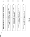
- FIG. 2 illustrates a flow chart of a discrete input determining method 200 in accordance with an embodiment of the present disclosure.
- the discrete input determining method 200 may include the steps as follows.
- a first input voltage is provided by biasing a discrete input.
- the first input voltage is divided into a second input voltage and a third input voltage.
- the first input voltage is less than the positive voltage of the discrete input
- the second input voltage is less than the first input voltage
- the third input voltage is less than the second input voltage.
- the second input voltage is compared with a reference voltage and a first output signal is outputted.
- the second input voltage when the discrete input is in an OPEN state, the second input voltage is larger than the reference voltage so that the first output is a logic high level; when the discrete input is in the positive voltage state, the second input voltage is larger than the reference voltage so that the first output is the logic high level; when the discrete input is in a GND state, the second input voltage is less than the reference voltage so that the first output voltage is a logic low level.
- the reference voltage is compared with the third input voltage and a second output is outputted.
- the reference voltage when the discrete input is in the OPEN state, the reference voltage is larger than the third input voltage so that the second output is the logic high level; when the discrete input is in the positive voltage state, the reference voltage is less than the third input voltage so that the second output is the logic low level; when the discrete input is in the GND state, the reference voltage is larger than the third input voltage so that the second output is the logic high level.
- a logic output is outputted by a logic function between the first output and the second output.
- the logic function comprises a logic AND function, wherein when the discrete input is in the OPEN state, the logic output is the logic high level; when the discrete input is in the positive voltage state or the GND state, the logic output is the logic low level.
- steps of the discrete input determining method in accordance with embodiments of the present disclosure are illustrated as functional blocks, the order of the blocks and the separation of the steps among the various blocks shown in FIG. 2 are not intended to be limiting.
- the blocks may be performed in a different order and a step associated with one block may be combined with one or more other blocks or may be subdivided into a number of blocks.
Landscapes
- Physics & Mathematics (AREA)
- General Physics & Mathematics (AREA)
- Logic Circuits (AREA)
- Semiconductor Integrated Circuits (AREA)
Abstract
Description
- This disclosure relates generally to the field of aircraft, and more particularly to a discrete input determining circuit and a discrete input determining method.
- Avionics products often provide circuits to read, ascertain or otherwise determine discrete inputs from other equipment in the aircraft. The discrete inputs may conform, for example, to one of two types: OPEN/GND or 28V/OPEN. Avionics products have typically used two different circuits to accommodate the two discrete types, providing internal pullups for the OPEN/GND discrete input and internal pulldowns for 28V/OPEN discrete input. Therefore, the avionics products have frequently provided a quantity of each circuit type to cover a variety of possible aircraft applications. For any given application, rarely are all the discrete inputs of both types utilized, and often there is a shortage of one type or the other. This may result in valuable hardware being left unused, reducing the flexibility and cost-effectiveness of the product.
- In one aspect of the present disclosure, a discrete input determining circuit is provided. The discrete input determining circuit comprises an input biasing network connected to a discrete input for providing a first input voltage, a voltage divider network for dividing the first input voltage into a second input voltage and a third input voltage, a first comparator and a second comparator. A non-inverting input terminal of the first comparator receives the second input voltage, and an inverting input terminal of the second comparator receives the third input voltage. An inverting input terminal of the first comparator and a non-inverting input terminal of the second comparator receive a reference voltage, and an output terminal of the first comparator and an output terminal of the second comparator are configured to provide a logic output.
- In another aspect of the present disclosure, a discrete input determining method is provided. The discrete input determining method comprises biasing the discrete input to provide a first input voltage, dividing the first input voltage into a second input voltage and a third input voltage, comparing the second input with a reference voltage and outputting a first output, comparing the reference voltage with the third input and outputting a second output, and outputting a logic output by a logic function between the first output and the second output.
- These and other features, aspects, and advantages of the present disclosure will become better understood when the following detailed description is read with reference to the accompanying drawings in which like characters represent like parts throughout the drawings, wherein:
-
FIG. 1 is an example schematic diagram of a discrete input determining circuit in accordance with aspects described herein; and -
FIG. 2 is an example flow chart of a discrete input determining method in accordance with aspects described herein. - Embodiments of the present disclosure will be described hereinbelow with reference to the accompanying drawings. In the following description, well-known functions or constructions are not described in detail to avoid obscuring the disclosure in unnecessary detail.
- Unless defined otherwise, technical and scientific terms used herein have the same meaning as is commonly understood by one of ordinary skill in the art to which this disclosure belongs. The terms "first", "second", and the like, as used herein do not denote any order, quantity, or importance, but rather are used to distinguish one element from another. Also, the terms "a" and "an" do not denote a limitation of quantity, but rather denote the presence of at least one of the referenced items. The term "or" is meant to be inclusive and mean either or all of the listed items. The use of "including," "comprising" or "having" and variations thereof herein are meant to encompass the items listed thereafter and equivalents thereof as well as additional items. The terms "connected" and "coupled" are not restricted to physical or mechanical connections or couplings, and can include electrical connections or couplings, whether direct or indirect. In addition, Terms indicating specific locations, such as "top", "bottom", "left", and "right", are descriptions with reference to specific accompanying drawings. Embodiments disclosed in the present disclosure may be placed in a manner different from that shown in the figures. Therefore, the location terms used herein should not be limited to locations described in specific embodiments.
-
FIG. 1 illustrates a schematic diagram of a discreteinput determining circuit 100. As shown inFIG.1 , the discreteinput determining circuit 100 comprises aninput biasing network 110 connected to a discrete input for providing a first input voltage V1, avoltage divider network 120 for dividing the first input voltage V1 into a second input voltage V2 and a third input voltage V3, afirst comparator 130 and asecond comparator 140. A non-inverting input terminal "+" of thefirst comparator 130 receives the second input voltage V2, and an inverting input terminal "-" of thesecond comparator 140 receives the third input voltage V3. An inverting input terminal "-" of thefirst comparator 130 and a non-inverting input terminal "+" of thesecond comparator 140 receive a reference voltage Vref. An output terminal of thefirst comparator 130 and an output terminal of thesecond comparator 140 are configured to provide a logic output F. - In one embodiment, the
input biasing network 110 comprises afirst power supply 111 and a first resistive load R1. The first resistive load R1 is connected between the discrete input and thefirst power supply 111, and a node P1 between the discrete input and the first resistive load R1 is connected to thevoltage divider network 120. When the discrete input is in the OPEN state, the first input voltage V1 is a voltage at the node P1 and the first input voltage V1 is less than a positive voltage V+ of the discrete input, for example, the positive voltage V+ is equal to 28 volts. It is to be appreciated that 28 volts is used herein for illustrative purposes; however, virtually any voltage would be within the scope of the subject innovation. - The
voltage divider network 120 can include a second resistive load R2 and a third resistive load R3 connection in series between the node P1 and a ground. The second input voltage V2 is a voltage at a node P2 between the node P1 and the second resistive load R2, and the third input voltage V3 is a voltage at a node P3 between the second resistive load R2 and the third resistive load R3. In this case, the second input voltage V2 is less than the first input voltage V1, and the third input voltage V3 is less than the second input voltage V2. In another embodiment, thevoltage divider network 120 further comprises a fourth resistive load R4 connection in series between the node P1 and the node P2, in this case, the second input voltage V2 is less than the first input voltage V1. In one embodiment, when the discrete input is in an OPEN state, the first input voltage V1 is determined by the relationship among thefirst power supply 111, the first resistive load R1, the second resistive load R2, the third resistive load R3, and the fourth resistive load R4. - As for the
first comparator 130, the non-inverting input terminal "+" can be connected to the node P2 for receiving the second input voltage V2, and the inverting input terminal "-" receives the reference voltage Vref. For example, when the second input voltage V2 is larger than the reference voltage Vref, thefirst comparator 130 outputs a logic high level; when the second input voltage V2 is less than the reference voltage Vref, thefirst comparator 130 outputs a logic low level. As for thesecond comparator 140, the non-inverting input terminal "+" receives the reference voltage Vref, and the inverting input terminal "-" is connected to the node P3 for receiving the third input voltage V3. When the third input voltage V3 is larger than the reference voltage Vref, thesecond comparator 140 outputs the logic low level; when the third input voltage V3 is less than the reference voltage Vref, thesecond comparator 140 outputs the logic high level. In an optional embodiment, thefirst comparator 130 and thesecond comparator 140 can be replaced by a window comparator or a dual comparator. - The output terminal of the
first comparator 130 and the output terminal of thesecond comparator 140 can be open-collector type outputs that are wired together to implement a logic AND function so as to provide the logic output F, in this case, the discreteinput determining circuit 100 further comprises anoutput configuration network 150, wherein theoutput configuration network 150 comprises asecond power supply 151 and a fifth resistive load R5 connected between thesecond power supply 151 and the logic output F. - The discrete
input determining circuit 100 can accommodate both OPEN/GND and 28V/OPEN discrete input types, and application of the discrete input determining circuit is more flexible and cost effective. The logic output can be routed to any general-purpose input or output (GPIO) pin on a microprocessor or a field programmable gate array (FPGA) used for the host product data processing. -
FIG. 2 illustrates a flow chart of a discreteinput determining method 200 in accordance with an embodiment of the present disclosure. The discreteinput determining method 200 may include the steps as follows. - In
step 201, a first input voltage is provided by biasing a discrete input. - In
step 202, the first input voltage is divided into a second input voltage and a third input voltage. In one embodiment, the first input voltage is less than the positive voltage of the discrete input, and the second input voltage is less than the first input voltage, and the third input voltage is less than the second input voltage. - In
step 203, the second input voltage is compared with a reference voltage and a first output signal is outputted. In one embodiment, when the discrete input is in an OPEN state, the second input voltage is larger than the reference voltage so that the first output is a logic high level; when the discrete input is in the positive voltage state, the second input voltage is larger than the reference voltage so that the first output is the logic high level; when the discrete input is in a GND state, the second input voltage is less than the reference voltage so that the first output voltage is a logic low level. - In
step 204, the reference voltage is compared with the third input voltage and a second output is outputted. In one embodiment, when the discrete input is in the OPEN state, the reference voltage is larger than the third input voltage so that the second output is the logic high level; when the discrete input is in the positive voltage state, the reference voltage is less than the third input voltage so that the second output is the logic low level; when the discrete input is in the GND state, the reference voltage is larger than the third input voltage so that the second output is the logic high level. - In
step 205, a logic output is outputted by a logic function between the first output and the second output. In one embodiment, the logic function comprises a logic AND function, wherein when the discrete input is in the OPEN state, the logic output is the logic high level; when the discrete input is in the positive voltage state or the GND state, the logic output is the logic low level. - While steps of the discrete input determining method in accordance with embodiments of the present disclosure are illustrated as functional blocks, the order of the blocks and the separation of the steps among the various blocks shown in
FIG. 2 are not intended to be limiting. For example, the blocks may be performed in a different order and a step associated with one block may be combined with one or more other blocks or may be subdivided into a number of blocks. - While the disclosure has been illustrated and described in typical embodiments, it is not intended to be limited to the details shown, since various modifications and substitutions can be made without departing in any way from the spirit of the present disclosure. As such, further modifications and equivalents of the disclosure herein disclosed may occur to persons skilled in the art using no more than routine experimentation, and all such modifications and equivalents are believed to be within the scope of the disclosure as defined by the following claims.
Claims (13)
- A discrete input determining circuit (100), comprising:an input biasing network (110) connected to a discrete input for providing a first input voltage (V1);a voltage divider network (120) for dividing the first input voltage (V1) into a second input voltage (V2) and a third input voltage (V3);a first comparator (130), wherein a non-inverting input terminal of the first comparator receives the second input voltage (V2); anda second comparator (140), wherein an inverting input terminal of the second comparator receives the third input voltage (V3);wherein an inverting input terminal of the first comparator and a non-inverting input terminal of the second comparator receive a reference voltage (Vref), and an output terminal of the first comparator and an output terminal of the second comparator are configured to provide a logic output (F).
- The discrete input determining circuit according to claim 1, wherein the input biasing network comprises a first power supply (151) and a first resistive load (R1) connected between the discrete input and the first power supply, and a node (Pi) between the discrete input and the first resistive load is connected to the voltage divider network.
- The discrete input determining circuit according to either of claim 1 or 2, wherein the first input voltage is less than a positive voltage of the discrete input.
- The discrete input determining circuit according to any preceding claim, wherein the voltage divider network comprises a second resistive load (R2) between the second input voltage and the third input voltage and a third resistive load (R3) between the third input voltage and a ground.
- The discrete input determining circuit according to claim 4, wherein the voltage divider network further comprises a fourth resistive load (R4) between the first input voltage and the second input voltage.
- The discrete input determining circuit according to any preceding claim, wherein the output terminal of the first comparator and the output terminal of the second comparator are wired together to implement a logic AND function so as to provide the logic output.
- The discrete input determining circuit according to claim 6, further comprising an output configuration network (150) comprising a second power supply (151) and a fifth resistive load (R5) connected between the second power supply and the logic output.
- A method of determining a discrete input, comprising:biasing (201) the discrete input to provide a first input voltage;dividing (202) the first input voltage into a second input voltage and a third input voltage;comparing (203) the second input with a reference voltage and outputting a first output;comparing (204) the reference voltage with the third input and outputting a second output; andoutputting (205) a logic output by a logic function between the first output and the second output.
- The method according to claim 8, wherein the first input voltage is less than a positive voltage of the discrete input, and the second input voltage is less than the first input voltage, and the third input voltage is less than the second input voltage.
- The method according to claim 9, wherein when the discrete input is in an OPEN state, the second input voltage is larger than the reference voltage so that the first output is a logic high level, and the reference voltage is larger than the third input voltage so that the second output is the logic high level.
- The method according to either of claim 9 or 10, wherein when the discrete input is in a positive voltage state, the second input voltage is larger than the reference voltage so that the first output is a logic high level, and the reference voltage is less than the third input voltage so that the second output is a logic low level.
- The method according to any of claims 9 to 11, wherein when the discrete input is in a GND state, the second input voltage is less than the reference voltage so that the first output is a logic low level, and the reference voltage is larger than the third input voltage so that the second output is a logic high level.
- The method according to any of claims 8 to 12, wherein the logic function comprises a logic AND function, wherein the logic output is a logic high level when the discrete input is in an OPEN state, the logic output is a logic low level when the discrete input is in a GND state, and the logic output is a logic low level when the discrete input is in a positive voltage state.
Applications Claiming Priority (1)
| Application Number | Priority Date | Filing Date | Title |
|---|---|---|---|
| US15/726,809 US10365304B2 (en) | 2017-10-06 | 2017-10-06 | Discrete input determining circuit and method |
Publications (2)
| Publication Number | Publication Date |
|---|---|
| EP3467521A1 true EP3467521A1 (en) | 2019-04-10 |
| EP3467521B1 EP3467521B1 (en) | 2025-08-27 |
Family
ID=63722201
Family Applications (1)
| Application Number | Title | Priority Date | Filing Date |
|---|---|---|---|
| EP18198161.4A Active EP3467521B1 (en) | 2017-10-06 | 2018-10-02 | Discrete input determining circuit and method |
Country Status (2)
| Country | Link |
|---|---|
| US (2) | US10365304B2 (en) |
| EP (1) | EP3467521B1 (en) |
Families Citing this family (4)
| Publication number | Priority date | Publication date | Assignee | Title |
|---|---|---|---|---|
| US10365304B2 (en) * | 2017-10-06 | 2019-07-30 | Ge Aviation Systems Llc | Discrete input determining circuit and method |
| CN112098762B (en) * | 2020-09-22 | 2024-08-16 | 陕西千山航空电子有限责任公司 | Discrete switching value acquisition and detection circuit |
| FR3118490B1 (en) | 2020-12-30 | 2023-01-13 | Thales Sa | Discrete interface configured to manage at least two active states and one inactive state in a device |
| IT202200000683A1 (en) * | 2022-01-18 | 2023-07-18 | St Microelectronics Srl | TEST SYSTEM OF AN ELECTRONIC CIRCUIT, IN PARTICULAR INTEGRATED CIRCUIT, INCLUDING A VOLTAGE MONITORING CIRCUIT AND CORRESPONDING PROCEDURE AND COMPUTER PRODUCT |
Citations (5)
| Publication number | Priority date | Publication date | Assignee | Title |
|---|---|---|---|---|
| EP0556549A1 (en) * | 1992-02-20 | 1993-08-25 | Motorola, Inc. | A discriminator device |
| EP0652517A2 (en) * | 1993-11-05 | 1995-05-10 | Ilc Data Device Corporation | Multiple channel discrete to digital interface |
| FR2854286A1 (en) * | 2003-04-24 | 2004-10-29 | Honeywell | Processing unit input stage, has biased input and two comparators for comparing input voltage to two threshold voltages, in order to supply to processing circuit two bits representative of type of sensor connected to the input |
| US20070080007A1 (en) * | 2005-10-06 | 2007-04-12 | Denso Corporation | Electric power generation control apparatus |
| EP3396399A1 (en) * | 2017-04-11 | 2018-10-31 | Hamilton Sundstrand Corporation | Voltage monitor self testing |
Family Cites Families (27)
| Publication number | Priority date | Publication date | Assignee | Title |
|---|---|---|---|---|
| US4055777A (en) | 1976-11-02 | 1977-10-25 | The United States Of America As Represented By The Administrator Of The National Aeronautics And Space Administration | Window comparator |
| US4321543A (en) * | 1980-04-14 | 1982-03-23 | Rca Corporation | Three-condition display system |
| JP2768520B2 (en) | 1989-02-17 | 1998-06-25 | ローベルト ボツシユ ゲゼルシヤフト ミツト ベシユレンクテル ハフツング | Network Interface |
| US5440254A (en) * | 1992-10-20 | 1995-08-08 | Exar Corporation | Accurate low voltage detect circuit |
| US5488323A (en) | 1994-12-14 | 1996-01-30 | United Technologies Corporation | True hysteresis window comparator for use in monitoring changes in switch resistance |
| FR2772923B1 (en) | 1997-12-23 | 2000-03-17 | Sextant Avionique | ELECTRONIC ELECTRICAL VOLTAGE MONITORING CIRCUIT |
| JP2004191333A (en) * | 2002-12-13 | 2004-07-08 | Matsushita Electric Ind Co Ltd | Binary power supply voltage detection circuit |
| US8344638B2 (en) * | 2008-07-29 | 2013-01-01 | Point Somee Limited Liability Company | Apparatus, system and method for cascaded power conversion |
| US7928744B2 (en) | 2008-12-02 | 2011-04-19 | Analog Devices, Inc. | Monitoring circuit having a self test function |
| GB2484442B (en) * | 2009-07-28 | 2013-12-25 | Skyworks Solutions Inc | Process, voltage, and temperature sensor |
| US8823418B2 (en) * | 2009-09-17 | 2014-09-02 | Taiwan Semiconductor Manufacturing Co., Ltd. | Power on detection circuit |
| JP4849164B2 (en) | 2009-09-29 | 2012-01-11 | 株式会社デンソー | Voltage monitoring device |
| US8461810B2 (en) * | 2009-12-17 | 2013-06-11 | Magnachip Semiconductor, Ltd. | Circuit for generating boosted voltage and method for operating the same |
| US8476836B2 (en) * | 2010-05-07 | 2013-07-02 | Cree, Inc. | AC driven solid state lighting apparatus with LED string including switched segments |
| US8645583B2 (en) * | 2010-09-23 | 2014-02-04 | Intersil Americas Inc. | Zero pin serial interface |
| US8816654B2 (en) | 2010-09-27 | 2014-08-26 | Cooper Technologies Company | Universal-voltage discrete input circuit |
| CN201893771U (en) | 2010-11-19 | 2011-07-06 | 陕西千山航空电子有限责任公司 | Universal interface circuit for discrete magnitude acquisition of airborne equipment |
| US9329063B2 (en) * | 2011-02-04 | 2016-05-03 | Semiconductor Components Industries, Llc | Electronic device with flexible data and power interface |
| US8373408B2 (en) | 2011-02-22 | 2013-02-12 | Sendyne Corporation | High precision algorithmically assisted voltage divider with fault detection |
| US8710872B2 (en) * | 2012-05-18 | 2014-04-29 | Infineon Technologies Austria Ag | Driver circuit for driving semiconductor switches |
| US8868294B2 (en) * | 2012-09-28 | 2014-10-21 | Firestone Industrial Products Company, Llc | Adjustable hysteresis circuit for control of air suspension |
| CN202998052U (en) | 2012-11-16 | 2013-06-12 | 深圳市多尼卡电子技术有限公司 | Discrete input control circuit and airplane electronic device |
| CN202995310U (en) | 2012-11-16 | 2013-06-12 | 深圳市多尼卡电子技术有限公司 | Discrete signal control circuit and airplane electronic device |
| JP5972808B2 (en) * | 2013-01-30 | 2016-08-17 | ルネサスエレクトロニクス株式会社 | Monitor circuit, semiconductor integrated circuit, semiconductor device, and power supply voltage control method thereof |
| CN103618524B (en) | 2013-11-27 | 2016-02-24 | 中国航空工业集团公司第六三一研究所 | A kind for the treatment of circuit of general discrete amount and method |
| KR102229022B1 (en) * | 2014-03-18 | 2021-03-17 | 삼성전자주식회사 | Device of detecting card having magnetic field monitor and System including the same |
| US10365304B2 (en) * | 2017-10-06 | 2019-07-30 | Ge Aviation Systems Llc | Discrete input determining circuit and method |
-
2017
- 2017-10-06 US US15/726,809 patent/US10365304B2/en active Active
-
2018
- 2018-10-02 EP EP18198161.4A patent/EP3467521B1/en active Active
-
2019
- 2019-07-26 US US16/522,839 patent/US10690702B2/en active Active
Patent Citations (5)
| Publication number | Priority date | Publication date | Assignee | Title |
|---|---|---|---|---|
| EP0556549A1 (en) * | 1992-02-20 | 1993-08-25 | Motorola, Inc. | A discriminator device |
| EP0652517A2 (en) * | 1993-11-05 | 1995-05-10 | Ilc Data Device Corporation | Multiple channel discrete to digital interface |
| FR2854286A1 (en) * | 2003-04-24 | 2004-10-29 | Honeywell | Processing unit input stage, has biased input and two comparators for comparing input voltage to two threshold voltages, in order to supply to processing circuit two bits representative of type of sensor connected to the input |
| US20070080007A1 (en) * | 2005-10-06 | 2007-04-12 | Denso Corporation | Electric power generation control apparatus |
| EP3396399A1 (en) * | 2017-04-11 | 2018-10-31 | Hamilton Sundstrand Corporation | Voltage monitor self testing |
Non-Patent Citations (1)
| Title |
|---|
| N.A. N.A.: "TPS3700-Q1 Window Comparator for Over-and Undervoltage Detection", 1 July 2017 (2017-07-01), pages 1 - 26, XP055558478, Retrieved from the Internet <URL:http://www.ti.com/lit/ds/symlink/tps3700-q1.pdf> [retrieved on 20190219] * |
Also Published As
| Publication number | Publication date |
|---|---|
| US10365304B2 (en) | 2019-07-30 |
| US10690702B2 (en) | 2020-06-23 |
| EP3467521B1 (en) | 2025-08-27 |
| US20190346488A1 (en) | 2019-11-14 |
| US20190107565A1 (en) | 2019-04-11 |
Similar Documents
| Publication | Publication Date | Title |
|---|---|---|
| US10690702B2 (en) | Discrete input determining circuit and method | |
| US9484920B2 (en) | Switching circuit and electronic device | |
| US10146265B1 (en) | Main board slot power control circuit | |
| US20080010406A1 (en) | Apparatus and method for discerning a host interface | |
| CN110287361A (en) | A kind of personage's picture screening technique and device | |
| CN206627597U (en) | One kind detection USB socket water inlet open circuit potential | |
| US7459903B1 (en) | Multi-level voltage detection circuit | |
| US20200004709A1 (en) | Adaption Apparatus, And Device Identification Method And Apparatus | |
| US20130311120A1 (en) | Battery voltage detection method and apparatus | |
| US20160139653A1 (en) | Computer system and matching circuit thereof | |
| US8840425B2 (en) | Connector apparatus and adapter apparatus with indication function | |
| WO2016070484A1 (en) | Feedback separated circuit, and motherboard and daughterboard combination detection method therefor | |
| US20130127447A1 (en) | Electrical parameter detection device for peripheral component interconnect devices | |
| CN107210744B (en) | Connector component information detection | |
| CN109189144A (en) | Method, device and system for controlling power supply voltage | |
| EP2753040A1 (en) | Terminating resistance generation device for differential input mode communication and differential input mode communication device | |
| US6246210B1 (en) | System for identifying electric devices | |
| US20140185250A1 (en) | Motherboard with compatible interface | |
| CN108804647A (en) | A kind of method and device of video sequence | |
| CN113835808B (en) | Display screen adaptation method, device, equipment and storage medium | |
| US9466981B2 (en) | Signal line power receiving circuit, signal line power supply circuit and signal line power supply system | |
| US20160233624A1 (en) | Electronic device and charging interface | |
| US9793665B2 (en) | Bar juice electronic device connection system | |
| CN112114264A (en) | Detection system for battery electric quantity | |
| KR20140092547A (en) | USB OTG auto change device |
Legal Events
| Date | Code | Title | Description |
|---|---|---|---|
| PUAI | Public reference made under article 153(3) epc to a published international application that has entered the european phase |
Free format text: ORIGINAL CODE: 0009012 |
|
| STAA | Information on the status of an ep patent application or granted ep patent |
Free format text: STATUS: THE APPLICATION HAS BEEN PUBLISHED |
|
| AK | Designated contracting states |
Kind code of ref document: A1 Designated state(s): AL AT BE BG CH CY CZ DE DK EE ES FI FR GB GR HR HU IE IS IT LI LT LU LV MC MK MT NL NO PL PT RO RS SE SI SK SM TR |
|
| AX | Request for extension of the european patent |
Extension state: BA ME |
|
| STAA | Information on the status of an ep patent application or granted ep patent |
Free format text: STATUS: REQUEST FOR EXAMINATION WAS MADE |
|
| 17P | Request for examination filed |
Effective date: 20191010 |
|
| RBV | Designated contracting states (corrected) |
Designated state(s): AL AT BE BG CH CY CZ DE DK EE ES FI FR GB GR HR HU IE IS IT LI LT LU LV MC MK MT NL NO PL PT RO RS SE SI SK SM TR |
|
| STAA | Information on the status of an ep patent application or granted ep patent |
Free format text: STATUS: EXAMINATION IS IN PROGRESS |
|
| 17Q | First examination report despatched |
Effective date: 20210921 |
|
| GRAP | Despatch of communication of intention to grant a patent |
Free format text: ORIGINAL CODE: EPIDOSNIGR1 |
|
| STAA | Information on the status of an ep patent application or granted ep patent |
Free format text: STATUS: GRANT OF PATENT IS INTENDED |
|
| RIC1 | Information provided on ipc code assigned before grant |
Ipc: G01R 31/00 20060101ALN20250318BHEP Ipc: G01R 19/165 20060101AFI20250318BHEP |
|
| INTG | Intention to grant announced |
Effective date: 20250327 |
|
| GRAS | Grant fee paid |
Free format text: ORIGINAL CODE: EPIDOSNIGR3 |
|
| GRAA | (expected) grant |
Free format text: ORIGINAL CODE: 0009210 |
|
| STAA | Information on the status of an ep patent application or granted ep patent |
Free format text: STATUS: THE PATENT HAS BEEN GRANTED |
|
| AK | Designated contracting states |
Kind code of ref document: B1 Designated state(s): AL AT BE BG CH CY CZ DE DK EE ES FI FR GB GR HR HU IE IS IT LI LT LU LV MC MK MT NL NO PL PT RO RS SE SI SK SM TR |
|
| REG | Reference to a national code |
Ref country code: GB Ref legal event code: FG4D |
|
| REG | Reference to a national code |
Ref country code: CH Ref legal event code: EP |
|
| REG | Reference to a national code |
Ref country code: DE Ref legal event code: R096 Ref document number: 602018084926 Country of ref document: DE |
|
| REG | Reference to a national code |
Ref country code: IE Ref legal event code: FG4D |
|
| P01 | Opt-out of the competence of the unified patent court (upc) registered |
Free format text: CASE NUMBER: UPC_APP_4693_3467521/2025 Effective date: 20250826 |
|
| PGFP | Annual fee paid to national office [announced via postgrant information from national office to epo] |
Ref country code: GB Payment date: 20250923 Year of fee payment: 8 |
|
| PGFP | Annual fee paid to national office [announced via postgrant information from national office to epo] |
Ref country code: FR Payment date: 20250923 Year of fee payment: 8 |
|
| REG | Reference to a national code |
Ref country code: NL Ref legal event code: MP Effective date: 20250827 |
|
| PG25 | Lapsed in a contracting state [announced via postgrant information from national office to epo] |
Ref country code: IS Free format text: LAPSE BECAUSE OF FAILURE TO SUBMIT A TRANSLATION OF THE DESCRIPTION OR TO PAY THE FEE WITHIN THE PRESCRIBED TIME-LIMIT Effective date: 20251227 |
|
| PGFP | Annual fee paid to national office [announced via postgrant information from national office to epo] |
Ref country code: DE Payment date: 20250902 Year of fee payment: 8 |
|
| PG25 | Lapsed in a contracting state [announced via postgrant information from national office to epo] |
Ref country code: NO Free format text: LAPSE BECAUSE OF FAILURE TO SUBMIT A TRANSLATION OF THE DESCRIPTION OR TO PAY THE FEE WITHIN THE PRESCRIBED TIME-LIMIT Effective date: 20251127 |
|
| REG | Reference to a national code |
Ref country code: LT Ref legal event code: MG9D |
|
| PG25 | Lapsed in a contracting state [announced via postgrant information from national office to epo] |
Ref country code: PT Free format text: LAPSE BECAUSE OF FAILURE TO SUBMIT A TRANSLATION OF THE DESCRIPTION OR TO PAY THE FEE WITHIN THE PRESCRIBED TIME-LIMIT Effective date: 20251229 |
|
| PG25 | Lapsed in a contracting state [announced via postgrant information from national office to epo] |
Ref country code: FI Free format text: LAPSE BECAUSE OF FAILURE TO SUBMIT A TRANSLATION OF THE DESCRIPTION OR TO PAY THE FEE WITHIN THE PRESCRIBED TIME-LIMIT Effective date: 20250827 |
|
| PG25 | Lapsed in a contracting state [announced via postgrant information from national office to epo] |
Ref country code: HR Free format text: LAPSE BECAUSE OF FAILURE TO SUBMIT A TRANSLATION OF THE DESCRIPTION OR TO PAY THE FEE WITHIN THE PRESCRIBED TIME-LIMIT Effective date: 20250827 Ref country code: NL Free format text: LAPSE BECAUSE OF FAILURE TO SUBMIT A TRANSLATION OF THE DESCRIPTION OR TO PAY THE FEE WITHIN THE PRESCRIBED TIME-LIMIT Effective date: 20250827 |
|
| PG25 | Lapsed in a contracting state [announced via postgrant information from national office to epo] |
Ref country code: GR Free format text: LAPSE BECAUSE OF FAILURE TO SUBMIT A TRANSLATION OF THE DESCRIPTION OR TO PAY THE FEE WITHIN THE PRESCRIBED TIME-LIMIT Effective date: 20251128 |
|
| PG25 | Lapsed in a contracting state [announced via postgrant information from national office to epo] |
Ref country code: SE Free format text: LAPSE BECAUSE OF FAILURE TO SUBMIT A TRANSLATION OF THE DESCRIPTION OR TO PAY THE FEE WITHIN THE PRESCRIBED TIME-LIMIT Effective date: 20250827 |
|
| PG25 | Lapsed in a contracting state [announced via postgrant information from national office to epo] |
Ref country code: LV Free format text: LAPSE BECAUSE OF FAILURE TO SUBMIT A TRANSLATION OF THE DESCRIPTION OR TO PAY THE FEE WITHIN THE PRESCRIBED TIME-LIMIT Effective date: 20250827 |
|
| PG25 | Lapsed in a contracting state [announced via postgrant information from national office to epo] |
Ref country code: PL Free format text: LAPSE BECAUSE OF FAILURE TO SUBMIT A TRANSLATION OF THE DESCRIPTION OR TO PAY THE FEE WITHIN THE PRESCRIBED TIME-LIMIT Effective date: 20250827 Ref country code: BG Free format text: LAPSE BECAUSE OF FAILURE TO SUBMIT A TRANSLATION OF THE DESCRIPTION OR TO PAY THE FEE WITHIN THE PRESCRIBED TIME-LIMIT Effective date: 20250827 |
|
| PG25 | Lapsed in a contracting state [announced via postgrant information from national office to epo] |
Ref country code: RS Free format text: LAPSE BECAUSE OF FAILURE TO SUBMIT A TRANSLATION OF THE DESCRIPTION OR TO PAY THE FEE WITHIN THE PRESCRIBED TIME-LIMIT Effective date: 20251127 |
|
| PG25 | Lapsed in a contracting state [announced via postgrant information from national office to epo] |
Ref country code: ES Free format text: LAPSE BECAUSE OF FAILURE TO SUBMIT A TRANSLATION OF THE DESCRIPTION OR TO PAY THE FEE WITHIN THE PRESCRIBED TIME-LIMIT Effective date: 20250827 |
|
| REG | Reference to a national code |
Ref country code: AT Ref legal event code: MK05 Ref document number: 1830482 Country of ref document: AT Kind code of ref document: T Effective date: 20250827 |
|
| PG25 | Lapsed in a contracting state [announced via postgrant information from national office to epo] |
Ref country code: RO Free format text: LAPSE BECAUSE OF FAILURE TO SUBMIT A TRANSLATION OF THE DESCRIPTION OR TO PAY THE FEE WITHIN THE PRESCRIBED TIME-LIMIT Effective date: 20250827 |
|
| PG25 | Lapsed in a contracting state [announced via postgrant information from national office to epo] |
Ref country code: SM Free format text: LAPSE BECAUSE OF FAILURE TO SUBMIT A TRANSLATION OF THE DESCRIPTION OR TO PAY THE FEE WITHIN THE PRESCRIBED TIME-LIMIT Effective date: 20250827 |
|
| PG25 | Lapsed in a contracting state [announced via postgrant information from national office to epo] |
Ref country code: DK Free format text: LAPSE BECAUSE OF FAILURE TO SUBMIT A TRANSLATION OF THE DESCRIPTION OR TO PAY THE FEE WITHIN THE PRESCRIBED TIME-LIMIT Effective date: 20250827 |
|
| PG25 | Lapsed in a contracting state [announced via postgrant information from national office to epo] |
Ref country code: AT Free format text: LAPSE BECAUSE OF FAILURE TO SUBMIT A TRANSLATION OF THE DESCRIPTION OR TO PAY THE FEE WITHIN THE PRESCRIBED TIME-LIMIT Effective date: 20250827 |
|
| PG25 | Lapsed in a contracting state [announced via postgrant information from national office to epo] |
Ref country code: IT Free format text: LAPSE BECAUSE OF FAILURE TO SUBMIT A TRANSLATION OF THE DESCRIPTION OR TO PAY THE FEE WITHIN THE PRESCRIBED TIME-LIMIT Effective date: 20250827 |
|
| PG25 | Lapsed in a contracting state [announced via postgrant information from national office to epo] |
Ref country code: CZ Free format text: LAPSE BECAUSE OF FAILURE TO SUBMIT A TRANSLATION OF THE DESCRIPTION OR TO PAY THE FEE WITHIN THE PRESCRIBED TIME-LIMIT Effective date: 20250827 |
|
| PG25 | Lapsed in a contracting state [announced via postgrant information from national office to epo] |
Ref country code: SK Free format text: LAPSE BECAUSE OF FAILURE TO SUBMIT A TRANSLATION OF THE DESCRIPTION OR TO PAY THE FEE WITHIN THE PRESCRIBED TIME-LIMIT Effective date: 20250827 Ref country code: EE Free format text: LAPSE BECAUSE OF FAILURE TO SUBMIT A TRANSLATION OF THE DESCRIPTION OR TO PAY THE FEE WITHIN THE PRESCRIBED TIME-LIMIT Effective date: 20250827 |
|
| REG | Reference to a national code |
Ref country code: CH Ref legal event code: H13 Free format text: ST27 STATUS EVENT CODE: U-0-0-H10-H13 (AS PROVIDED BY THE NATIONAL OFFICE) Effective date: 20260527 |
|
| REG | Reference to a national code |
Ref country code: DE Ref legal event code: R097 Ref document number: 602018084926 Country of ref document: DE |
|
| PG25 | Lapsed in a contracting state [announced via postgrant information from national office to epo] |
Ref country code: LU Free format text: LAPSE BECAUSE OF NON-PAYMENT OF DUE FEES Effective date: 20251002 |
|
| REG | Reference to a national code |
Ref country code: BE Ref legal event code: MM Effective date: 20251031 |
|
| PG25 | Lapsed in a contracting state [announced via postgrant information from national office to epo] |
Ref country code: LT Free format text: LAPSE BECAUSE OF FAILURE TO SUBMIT A TRANSLATION OF THE DESCRIPTION OR TO PAY THE FEE WITHIN THE PRESCRIBED TIME-LIMIT Effective date: 20250827 Ref country code: MC Free format text: LAPSE BECAUSE OF FAILURE TO SUBMIT A TRANSLATION OF THE DESCRIPTION OR TO PAY THE FEE WITHIN THE PRESCRIBED TIME-LIMIT Effective date: 20250827 |
|
| PLBE | No opposition filed within time limit |
Free format text: ORIGINAL CODE: 0009261 |
|
| STAA | Information on the status of an ep patent application or granted ep patent |
Free format text: STATUS: NO OPPOSITION FILED WITHIN TIME LIMIT |
|
| REG | Reference to a national code |
Ref country code: CH Ref legal event code: L10 Free format text: ST27 STATUS EVENT CODE: U-0-0-L10-L00 (AS PROVIDED BY THE NATIONAL OFFICE) Effective date: 20260708 |
|
| PG25 | Lapsed in a contracting state [announced via postgrant information from national office to epo] |
Ref country code: CH Free format text: LAPSE BECAUSE OF NON-PAYMENT OF DUE FEES Effective date: 20251031 Ref country code: BE Free format text: LAPSE BECAUSE OF NON-PAYMENT OF DUE FEES Effective date: 20251031 |
|
| 26N | No opposition filed |
Effective date: 20260528 |