EP3466341A1 - X-ray detector structure - Google Patents
X-ray detector structure Download PDFInfo
- Publication number
- EP3466341A1 EP3466341A1 EP18195865.3A EP18195865A EP3466341A1 EP 3466341 A1 EP3466341 A1 EP 3466341A1 EP 18195865 A EP18195865 A EP 18195865A EP 3466341 A1 EP3466341 A1 EP 3466341A1
- Authority
- EP
- European Patent Office
- Prior art keywords
- detector
- layer
- enclosure
- filler
- filler layer
- Prior art date
- Legal status (The legal status is an assumption and is not a legal conclusion. Google has not performed a legal analysis and makes no representation as to the accuracy of the status listed.)
- Granted
Links
Images



Classifications
-
- A—HUMAN NECESSITIES
- A61—MEDICAL OR VETERINARY SCIENCE; HYGIENE
- A61B—DIAGNOSIS; SURGERY; IDENTIFICATION
- A61B6/00—Apparatus or devices for radiation diagnosis; Apparatus or devices for radiation diagnosis combined with radiation therapy equipment
- A61B6/42—Arrangements for detecting radiation specially adapted for radiation diagnosis
- A61B6/4283—Arrangements for detecting radiation specially adapted for radiation diagnosis characterised by a detector unit being housed in a cassette
-
- A—HUMAN NECESSITIES
- A61—MEDICAL OR VETERINARY SCIENCE; HYGIENE
- A61B—DIAGNOSIS; SURGERY; IDENTIFICATION
- A61B6/00—Apparatus or devices for radiation diagnosis; Apparatus or devices for radiation diagnosis combined with radiation therapy equipment
-
- A—HUMAN NECESSITIES
- A61—MEDICAL OR VETERINARY SCIENCE; HYGIENE
- A61B—DIAGNOSIS; SURGERY; IDENTIFICATION
- A61B6/00—Apparatus or devices for radiation diagnosis; Apparatus or devices for radiation diagnosis combined with radiation therapy equipment
- A61B6/10—Safety means specially adapted therefor
- A61B6/102—Protection against mechanical damage, e.g. anti-collision devices
-
- A—HUMAN NECESSITIES
- A61—MEDICAL OR VETERINARY SCIENCE; HYGIENE
- A61B—DIAGNOSIS; SURGERY; IDENTIFICATION
- A61B6/00—Apparatus or devices for radiation diagnosis; Apparatus or devices for radiation diagnosis combined with radiation therapy equipment
- A61B6/42—Arrangements for detecting radiation specially adapted for radiation diagnosis
-
- A—HUMAN NECESSITIES
- A61—MEDICAL OR VETERINARY SCIENCE; HYGIENE
- A61B—DIAGNOSIS; SURGERY; IDENTIFICATION
- A61B6/00—Apparatus or devices for radiation diagnosis; Apparatus or devices for radiation diagnosis combined with radiation therapy equipment
- A61B6/44—Constructional features of apparatus for radiation diagnosis
-
- A—HUMAN NECESSITIES
- A61—MEDICAL OR VETERINARY SCIENCE; HYGIENE
- A61B—DIAGNOSIS; SURGERY; IDENTIFICATION
- A61B6/00—Apparatus or devices for radiation diagnosis; Apparatus or devices for radiation diagnosis combined with radiation therapy equipment
- A61B6/44—Constructional features of apparatus for radiation diagnosis
- A61B6/4411—Constructional features of apparatus for radiation diagnosis the apparatus being modular
-
- G—PHYSICS
- G01—MEASURING; TESTING
- G01T—MEASUREMENT OF NUCLEAR OR X-RADIATION
- G01T1/00—Measuring X-radiation, gamma radiation, corpuscular radiation, or cosmic radiation
-
- G—PHYSICS
- G01—MEASURING; TESTING
- G01T—MEASUREMENT OF NUCLEAR OR X-RADIATION
- G01T1/00—Measuring X-radiation, gamma radiation, corpuscular radiation, or cosmic radiation
- G01T1/16—Measuring radiation intensity
- G01T1/24—Measuring radiation intensity with semiconductor detectors
- G01T1/244—Auxiliary details, e.g. casings, cooling, damping or insulation against damage by, e.g. heat, pressure or the like
Definitions
- the materials utilized to for the components of the detector are rigid in nature in order to provide structural integrity to the detector and to provide a level of protection for the internal components.
- significant stresses are applied to the detector, such as when placing a patient in a standing position on the detector prior to obtaining the x-ray image with the detector and imaging system.
- shock mounts are capable of only directing the forces applied to the enclosure directly through the mounts, without being able to significantly dissipate the effects of the applied force across the enclosure. Further, the inclusions of the shock mounts complicate the internal structure of the detector where space is at a premium. Also, the shock mounts do not address the effects of the force on the enclosure, and thus do not provide a significant benefit to the structure of the detector enclosure.
- the apertures 126 can be formed to extend completely through the filler/force distribution layer 124, or can be shaped to extend a specified depth or distance into the filler 124 without extending completely through the filler 124.
- the material forming the filler 124 can be shaped by injecting the material directly into the interior of the detector 14 such that the material conforms to the shape(s) of and fills the negative spaces between the particular layers of the detector 14 and around the internal component(s) where the filler 124 is to be positioned
Landscapes
- Health & Medical Sciences (AREA)
- Life Sciences & Earth Sciences (AREA)
- Engineering & Computer Science (AREA)
- Medical Informatics (AREA)
- Physics & Mathematics (AREA)
- High Energy & Nuclear Physics (AREA)
- Molecular Biology (AREA)
- Nuclear Medicine, Radiotherapy & Molecular Imaging (AREA)
- Biomedical Technology (AREA)
- Veterinary Medicine (AREA)
- Public Health (AREA)
- Optics & Photonics (AREA)
- Pathology (AREA)
- Radiology & Medical Imaging (AREA)
- Biophysics (AREA)
- Heart & Thoracic Surgery (AREA)
- Surgery (AREA)
- Animal Behavior & Ethology (AREA)
- General Health & Medical Sciences (AREA)
- General Physics & Mathematics (AREA)
- Spectroscopy & Molecular Physics (AREA)
- Measurement Of Radiation (AREA)
- Apparatus For Radiation Diagnosis (AREA)
Abstract
Description
- In order to obtain X-ray images of interior structures of a body, such as a piece of luggage or the body of a patient, various types of imaging systems are employed. In many prior art imaging systems, the detector is formed as a separable component from the remainder of the imaging system. The detector is formed as a cassette-like structure with a housing enclosing the components of the detector necessary to detect the impingement of X-rays thereon to form the X-ray image.
- In many detector structures, the cassette enclosure includes a rigid back cover secured to a front cover off the cassette. The enclosure contains various components for enabling the detector to function as desired, including an imager that is struck by the X-rays, different electronic components for receiving data from the imager, a backscatter shield and a power source for supplying power to the various component of the detector.
- The materials utilized to for the components of the detector are rigid in nature in order to provide structural integrity to the detector and to provide a level of protection for the internal components. However, when in use significant stresses are applied to the detector, such as when placing a patient in a standing position on the detector prior to obtaining the x-ray image with the detector and imaging system.
- In these situations, stepping on the detector causes the enclosure to deflect which can cause the enclosure and/or components within the enclosure to crack or deform as a result of the deflection and applied pressure. Further, in the event that the detector is dropped, the force of the shock on the impact can also cause damage to the enclosure and/or internal parts of the detector.
- In order to addresses these issues with the structure of the detector, prior art detectors include shock mounts disposed within the enclosure between the internal components and the enclosure. The mounts are formed of an elastomeric, rubber or similar material and operate to separate or indirectly connect the internal component with the enclosure at the specific mounting points/points of contact between the enclosure and the internal components. Upon stress or forces being applied to the enclosure, the compressible nature of the material forming the shock mounts enable the internal component to move within and/or shift with respect to the enclosure, e.g., from 2-3mm, in an attempt to minimize the effects of the force on the internal components.
- However, the shock mounts are capable of only directing the forces applied to the enclosure directly through the mounts, without being able to significantly dissipate the effects of the applied force across the enclosure. Further, the inclusions of the shock mounts complicate the internal structure of the detector where space is at a premium. Also, the shock mounts do not address the effects of the force on the enclosure, and thus do not provide a significant benefit to the structure of the detector enclosure.
- Accordingly, it is desirable to provide detector for an X-ray imaging system having an enclosure capable of effectively distributing forces applied to the enclosure to protect both the detector enclosure and the internal components of the enclosure.
- There is a need or desire for an enclosure for an x-ray detector that is capable of increasing the ability of the detector to withstand shock and other types of forces acting on the enclosure to prevent and/or limit damage to the internal components of the detector. The enclosure includes an internal filler/force distribution layer formed from a lightweight, rigid material such as rigid foam having suitable structure, such as a honeycomb or other lattice structure. The material is formed or shaped to fill a layer or portion of the interior of the detector that is otherwise empty space defined between the various internal components of the detector. The position and shape of the force distribution layer determines the path of load distribution across or through the enclosure away from the internal components of the detector and is optimized for shock absorption and/or load distribution.
- The force distribution layer acts as a load distributor, shock absorber, and/or chassis within the enclosure. The force distribution layer includes cutouts or pockets corresponding to the position of various internal components of the detector, such as batteries, and/or smaller cutouts surrounding groups of components located on the circuit boards disposed within the enclosure for the detector. The positioning of the force distribution layer enables a load or other force exerted on the enclosure to be distributed more evenly through the detector without putting stress on sensitive components or through the circuit boards without stressing the components of the circuit boards. For example, in the event of an individual steps onto the detector including the force distribution layer, the load is distributed via the force distribution layer through the enclosure from the front surface to the back surface. Additionally, as a result of this force distribution capability, an enclosure including the force distribution layer can eliminate the need for separate shock mountings, and/or structural support ribs on the enclosure. Further thinning of enclosure materials can also be made possible, since the planar stiffness of the enclosure front and back face are less essential.
- According to a further exemplary aspect of the invention, an x-ray detector includes an enclosure, an imager disposed within the enclosure, an electronics layer disposed within the enclosure and operably connected to the imager and at least one filler layer disposed within the enclosure and between the electronic layer and the enclosure.
- According to still a further aspect of the invention, a method for forming a detector for use in conjunction with an X-ray imaging system includes the steps of forming at least one filler layer of a high compressive strength, low density material, the at least one filler layer including a number of apertures extending at least partially through the at least one filler layer therein and positioning the at least one filler layer within an enclosure for the detector between an electronics layer and the enclosure in order to distribute forces acting on the detector through the detector.
- It should be understood that the brief description above is provided to introduce in simplified form a selection of concepts that are further described in the detailed description. It is not meant to identify key or essential features of the claimed subject matter, the scope of which is defined uniquely by the claims that follow the detailed description. Furthermore, the claimed subject matter is not limited to implementations that solve any disadvantages noted above or in any part of this disclosure.
- The drawings illustrate the preferred mode presently contemplated of carrying out the disclosure. In the drawings:
-
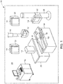
FIG. 1 is a pictorial view of a medical imaging system formed according to an exemplary non-limiting embodiment of the invention. -
FIG. 2 is an isometric view of an x-ray ray detector cassette/enclosure according to an exemplary non-limiting embodiment of the invention. -
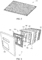
FIG. 3 is an exploded view of the detector cassette/enclosure ofFIG. 2 . -
FIG. 4 is an isometric view of a force distribution layer constructed according to an exemplary non-limiting embodiment of the invention. -
FIG. 5 is a top plan view of a force distribution layer mounted to an electronics layer according to another exemplary non-limiting embodiment of the invention. -
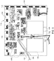
FIG. 6 is a top plan view of a force distribution layer constructed according to another exemplary non-limiting embodiment of the invention. -
FIG. 7 is a partially broken-away perspective view of the force distribution layer ofFIG. 6 . - In the following detailed description, reference is made to the accompanying drawings that form a part hereof, and in which is shown by way of illustration specific embodiments, which may be practiced. These embodiments are described in sufficient detail to enable those skilled in the art to practice the embodiments, and it is to be understood that other embodiments may be utilized and that logical, mechanical, electrical and other changes may be made without departing from the scope of the embodiments. The following detailed description is, therefore, not to be taken in a limiting sense.
-
FIG. 1 is a pictorial view of anexemplary imaging system 10 formed in accordance with an embodiment of the present invention. Various embodiments of the invention may be used with the exemplarymedical imaging system 10 as shown inFIG. 1 . Themedical imaging system 10 may be any type imaging system such as, for example, an x-ray imaging system or a tomosynthesis imaging system. Moreover, the various embodiments are not limited to medical imaging systems for imaging human subjects, but may include veterinary or non-medical systems for imaging non-human objects, or non-destructive testing systems (e.g. airport baggage systems) etc. - The
medical imaging system 10 in the preferred embodiment is a digitalradiography imaging system 10 that includes anx-ray source 12 and at least onedetector 14. In the exemplary embodiment, thedetector 14 is a portable x-ray detector. As shown inFIG. 2 , thedetector 14 may be utilized in various locations and applications, and in either a fixed state or a portable state. Thex-ray source 12 is mounted to agantry 16. Thegantry 16 may be movable to enable thex-ray source 12 to be properly positioned with respect to asubject 18 being imaged or to enable thex-ray source 12 to be moved from one imaging room to another. Optionally, thegantry 16 may be mounted to a floor or ceiling, for example. - When the
cassette holder 22 is coupled to thewall 24 or thepost 26, thecassette holder 22 is often referred to as a wall bucky. Moreover, thecassette holder 22 may fixedly installed in an imaging table 31. When installed in the imaging table 31, thecassette holder 22 may be referred to as a table bucky. In the fixed state, thedetector 14 receives power from thecassette holder 22. - The cassette holder or
bucky 22 also enables the x-ray detector to communicate with an imaging workstation, such as animaging workstation 30. During operation, information is transmitted from theworkstation 30 to thedetector 14 via wires (such as an Ethernet cable) in thecassette holder 22. Additionally, information generated by thedetector 14 may be transmitted to theworkstation 30 via wires (such as an Ethernet cable) in thecassette holder 22. The information that is generated and transferred may be at a rate higher than a wireless connection can support. Accordingly, in the fixed state, thedetector 14 is mounted in a fixed position to thecassette holder 22 and power and communication signals are transmitted from, and received by thedetector 14 via thecassette holder 22. - In another mode of operation, the
detector 14 is operated in the portable state. For example, in the portable state, thedetector 14 is installed into acharging bin 20. Thecharging bin 20 is configured to provide power to thedetector 14 to charge a battery (not shown) installed in thedetector 14, but does not provide a wired communication path between thedetector 14 and theimaging workstation 30. In another portable state, thedetector 14 receives operational power from the battery installed in thedetector 14. This portable state is also referred to herein as digital cassette mode. Additionally, operational and communication signals are transmitted wirelessly between thedetector 14 and theworkstation 30. For example, as shown inFIG. 1 , in the portable state, thedetector 14 may be positioned on a table 31 beneath the subject 18. Thedetector 14 may also be positioned on a separate table 33 that is adjacent to the subject 18. Accordingly, in the portable state, thedetector 14 is not coupled to thecassette holder 22. - Looking now at the exemplary illustrated embodiment shown in
FIGS. 2 and 3 , thedetector 14 includes ahousing 100 formed with afront cover 102 and arear cover 104. Thefront cover 102 andrear cover 104 are normally formed of a rigid and lightweight material on order to provide protection to the interior components of thedetector 14 without significantly increasing the weight of thedetector 14. In an exemplary embodiment, thefront cover 102 is formed of a material that is transparent to x-rays, such as a carbon fiber material, while therear cover 104 is formed from a metal, such as a lightweight magnesium alloy material. - Between the
front cover 102 andrear cover 104 the interior components of thedetector 14 include afoam layer 106 disposed immediately adjacent thefront cover 102 and present to provide a separation layer between the rigidfront cover 102 and animager 108 disposed adjacent thefoam layer 106. Theimager 108 is formed in a known manner of a material capable of detecting x-rays striking theimager 108 in order to provide image data concerning the impingements of the x-rays upon theimager 108. - Adjacent the
imager 108 but opposite thefoam layer 106 is located alead backscatter shield 110 present to capture any stray x-rays passing through or around theimager 108. Thebackscatter shield 110 is disposed on one side of asupport layer 112. Thesupport layer 112 provides internal structural support to thedetector 104 and can be formed of a lightweight and rigid material, such as a magnesium alloy. - Opposite the
shield 110, thesupport layer 112 provides an attachment point for theelectronics 114 that are operably connected to theimager 108 and that control the operation of thedetector 104. Theelectronics 114 can includedigital electronics 116 and/or scan/data processing electronics 118 that are operably connected to theimager 108 and to one another, as well as tobatteries 120 also disposed on thesupport layer 112. Therear cover 104 is secured to thefront cover 102 and thesupport layer 112 adjacent theelectronics 114 in order to provide a rigid enclosure 122 for the various components 106-120 within thedetector 14. - Referring now to
FIGS. 4-5 , between theelectronics 114 and therear cover 104 is disposed a chassis or filler/force distribution layer 124. Theforce distribution layer 124 is formed to fill the voids present in prior art detectors between theelectronics layer 114 and therear cover 104. Theforce distribution layer 124 is formed from a material having a high compressive strength and a low density, such that the material is capable of providing significant shock absorption/force transmission properties to thedetector 14 but without significantly increasing the overall weight of thedetector 14. Exemplary materials for use in forming the filler/force distribution layer 124 include honeycomb materials, foams, gels and rubber-like materials. In one exemplary embodiment, the material forming the filler/force distribution layer 124 is a generally rigid polymeric foam material having a density from 3 to 40 lbs/ft3 with a compressive strength of between 60-250psi. An example of such a material is are rigid polyurethane foams sold by General Plastics Mfg. Co., of Tacoma, WA under the tradename LAST-A-FOAM®. - The filler/
force distribution layer 124 is formed with an overall shape corresponding to the shape of the interior of thedetector 14 between theelectronics 114 and therear cover 104, and includesapertures 126 corresponding to the shape of the various components on the electronics layer 144, e.g., thedigital electronics 116, scan/data electronics 118 and/orbatteries 120. In this position, due to the location and the composition of the filler/force distribution layer 124, thelayer 124 can transmit and/or distribute any forces acting or exerted upon thedetector 14 directly and evenly through thedetector 14 from thefront cover 102 to therear cover 104, or vice versa. The location of thefiller 124 across the entire interior of thedetector 14 enables the filler/force distribution layer 124 to provide contact between thesupport layer 112 and therear cover 104 across theentire detector 14. In conjunction with the location of thelayer 124, the material forming the filler/force distribution layer 124 enables the filler/force distribution layer 124 can effectively distribute a force on thedetector 14 across the entire area of the filler/force distribution layer 124. Additionally, the material forming thelayer 124 can also result in a weight reduction through the elimination of the need for any load bearing ribs or shock mounts disposed within thedetector 14 and additional thinning of theenclosure 100, and where weight reduction from prior art detector structures of more than 1kg, and approximately 1.2kg. - In the configuration of the
filler 124 including theapertures 126, as shown in the exemplary embodiment ofFIG. 6 , the filler/force distribution layer 124 extends across theentire detector 14 such that a load or force applied to thefront cover 102 orrear cover 104 of thedetector 14 will be transferred through thefiller 124 and around the sensitive components on theelectronics layer 114 which will not receive a force from the load. In particular, as shown inFIG. 6 in those areas of theelectronics layer 114 formed at least in art with printed circuit boards (PCBs) 128 having individual or groups of sensitive electronic components 130 thereon, such as thedigital electronics 116 and/or scan/data electronics 118, theapertures 126 can be formed to closely conform the perimeter of the components 130 on thePCBs 128 in such a way that a force applied on thefront cover 102 of thedetector 14 is distributed through thefiller 124 to thePCB 128 and ultimately to adjacent layers, e.g., therear cover 104 and/orsupport layer 112, such that thefiller 124 enables the PCB(s) 128, but not the sensitive components 130 disposed on the PCB(s) 128, to function as a portion of a path for bearing load through thedetector 14. In addition, thefiller 124 can includechannels 132 that intersect the perimeter of thefiller 124 to allow forwired connections 134 to extend through thefiller 124 for connection to the selected components 130. - In order to provide the filler/
force distribution layer 124 with the desired shape and characteristics, the filler/force distribution layer 124 can be formed in a number of different suitable manners. For example, the material forming thefiller 124 can be formed in bulk using any suitable process and subsequently machined or otherwise shaped into the desired configuration. This shaping of the material into thefiller 124 can include, for example, laser cutting, machining or rastering the material into the desired shape including the overall shape for placement of thefiller 124 within thedetector 14 and for the shape of theapertures 126 within the filler/force distribution layer 124. Theapertures 126 can be formed to extend completely through the filler/force distribution layer 124, or can be shaped to extend a specified depth or distance into thefiller 124 without extending completely through thefiller 124. Alternatively, in another exemplary embodiment, the material forming thefiller 124 can be shaped by injecting the material directly into the interior of thedetector 14 such that the material conforms to the shape(s) of and fills the negative spaces between the particular layers of thedetector 14 and around the internal component(s) where thefiller 124 is to be positioned - In an alternative exemplary structure for and method of forming the filler/
force distribution layer 124, thefiller 124 may be manufactured with twosheets force distribution layer 124, as shown inFIGS. 7 and 8. In this exemplary embodiment, the aperture(s) 126 can be formed by cutting, machining, rastering or otherwise shaping the aperture(s) 126 within and/or through onesheet 136 and securing thesheet 136 to theother sheet 138. Further, in exemplary embodiments including one or more layers forming the filler/force distribution layer 124, thefiller 124 can be formed in a suitable additive manufacturing process, enabling the materials used in the different portions of thefiller 124, and/or the configuration of theapertures 126 to be closely controlled during manufacture of thefiller 124. - In addition, in the exemplary embodiment where the filler/
force distribution layer 124 includes multiple layers or materials, thefiller 124 can be formed with arigid plastic layer 136 combined with alayer 138 of softer rubber or other cushioning material that is positioned on or against with contact surfaces, such asPCBs 128, within thedetector 14. In this exemplary, embodiment, the softermaterial forming layer 138 can be formed to optimize the shock absorption capability of thefiller 124 to allow thefiller 124 to function as a shock mount between the points of contact of thelayer 138 with other components and/or layers within thedetector 14. Further, the filler/force distribution layer 124 can function as a chassis to enable circuit board(s) 128, therear cover 104,front cover 102, and/or layers of thedetector 14 to be mounted directly to thefiller 124 in a suitable manner, such as by using any suitable adhesive or mechanical fasteners. - In any of the previously described exemplary embodiments the filler/
force distribution layer 124 can be coated or sealed to contain the material forming thefiller 124 and avoiding the dissemination of any particles/dust of the material forming thelayer 124 within thedetector 14, and/or to add other attributes and/or enhancements to the material forming thelayer 124, such as anti-static and/or electrostatic property enhancing coatings, or flame retardant coatings, among others. - The written description uses examples to disclose the invention, including the preferred mode, and also to enable any person skilled in the art to practice the invention, including making and using any devices or systems and performing any incorporated methods. The patentable scope of the invention is defined by the claims, and may include other examples that occur to those skilled in the art. Such other examples are intended to be within the scope of the claims if they have structural elements that do not differ from the literal language of the claims, or if they include equivalent structural elements with insubstantial differences from the literal language of the claims.
- Various aspects and embodiments of the present invention are defined by the following numbered clauses:
- 1. An x-ray detector comprising:
- an enclosure;
- an imager disposed within the enclosure;
- an electronics layer disposed within the enclosure and operably connected to the imager; and
- at least one filler layer disposed within the enclosure and between the electronic layer and the enclosure.
- 2. The detector of clause 1, wherein the at least one filler layer is a material having a high compressive strength and a low density.
- 3. The detector of any preceding clause, wherein the material forming the at least one filler layer has a compressive strength of between 60psi-250psi.
- 4. The detector of any preceding clause, wherein the material forming the at least one filler layer has a density of between 3 lbs/ft3 to 40 lbs/ft3.
- 5. The detector of any preceding clause, wherein the material forming the at least one filler layer is a foam material.
- 6. The detector of any preceding clause, wherein the at least one filler layer includes a number of apertures formed therein, the apertures positioned over components of the electronics layer.
- 7. The detector of any preceding clause, wherein the electronics layer includes a circuit board on which the components are disposed, and wherein the at least one filler layer contacts the circuit board around the components.
- 8. The detector of any preceding clause, wherein the at least one filler layer is formed of multiple materials.
- 9. The detector of clause 8 further comprising:
- a first layer of a first material; and
- a second layer of a second material, wherein the second layer is adjacent to the first layer.
- 10. The detector of clause 9, wherein the first material and the second material have different compressive strength.
- 11. The detector of any preceding clause, wherein the first layer at least partially overlays the second layer.
- 12. The detector of any preceding clause, wherein at least one of the first layer or the second layer includes a number of apertures therein.
- 13. The detector of any preceding clause, wherein the filler layer fills an entire interior space within the enclosure between the electronics layer and the enclosure.
- 14. A method for forming a detector for use in conjunction with an X-ray imaging system, the method comprising:
- forming at least one filler layer of a high compressive strength, low density material, the at least one filler layer including a number of apertures extending at least partially through the at least one filler layer therein; and
- positioning the at least one filler layer within an enclosure for the detector between an electronics layer and the enclosure in order to distribute forces acting on the detector through the detector.
- 15. The method of
clause 14, wherein the steps of forming the at least one filler layer and positioning the at least one filler layer within the enclosure are performed simultaneously. - 16. The method of any preceding clause, wherein the step of forming the at least one filler layer comprises:
- forming a first layer;
- forming a second layer; and
- placing the first layer and the second layer adjacent to one another.
- 17. The method of any preceding clause, wherein the step of first layer and the second layer to one another comprises additively manufacturing the first layer and the second layer.
- 18. The method of any preceding clause, wherein the step of positioning the at least one filler layer comprises placing the number of apertures over components disposed on the electronics layer.
- 19. The method of any preceding clause wherein the step of placing the first layer and the second layer adjacent to one another comprises attaching the first layer and the second layer to one another.
Claims (15)
- An x-ray detector (14) comprising:an enclosure (122);an imager (102) disposed within the enclosure;an electronics layer (114) disposed within the enclosure and operably connected to the imager; andat least one filler layer (124) disposed within the enclosure and between the electronic layer and the enclosure.
- The detector (14) of claim 1, wherein the at least one filler layer is a material having a high compressive strength and a low density.
- The detector (14) of any preceding claim, wherein the material forming the at least one filler layer has a compressive strength of between 60psi-250psi.
- The detector (14) of any preceding claim, wherein the material forming the at least one filler layer has a density of between 3 lbs/ft3 to 40 lbs/ft3.
- The detector (14) of any preceding claim, wherein the material forming the at least one filler layer is a foam material.
- The detector (14) of any preceding claim, wherein the at least one filler layer includes a number of apertures formed therein, the apertures positioned over components of the electronics layer.
- The detector (14) of any preceding claim, wherein the electronics layer includes a circuit board on which the components are disposed, and wherein the at least one filler layer contacts the circuit board around the components.
- The detector (14) of any preceding claim, wherein the at least one filler layer is formed of multiple materials.
- The detector (14) of any preceding claim further comprising:a first layer of a first material; anda second layer of a second material, wherein the second layer is adjacent to the first layer.
- The detector (14) of claim 9, wherein the first material and the second material have different compressive strength.
- The detector (14) of claim 9 or 10, wherein the first layer at least partially overlays the second layer.
- The detector (14) of claim 9, 10 or 11, wherein at least one of the first layer or the second layer includes a number of apertures therein.
- The detector (14) of any preceding claim, wherein the filler layer (124) fills an entire interior space within the enclosure between the electronics layer and the enclosure.
- A method for forming a detector (14) for use in conjunction with an X-ray imaging system, the method comprising:forming at least one filler layer (124) of a high compressive strength, low density material, the at least one filler layer including a number of apertures extending at least partially through the at least one filler layer therein; andpositioning the at least one filler layer within an enclosure for the detector between an electronics layer and the enclosure in order to distribute forces acting on the detector through the detector.
- The method of claim 14, wherein the steps of forming the at least one filler layer (124) and positioning the at least one filler layer within the enclosure are performed simultaneously.
Applications Claiming Priority (1)
| Application Number | Priority Date | Filing Date | Title |
|---|---|---|---|
| US15/719,999 US10045748B1 (en) | 2017-09-29 | 2017-09-29 | X-ray detector structure |
Publications (2)
| Publication Number | Publication Date |
|---|---|
| EP3466341A1 true EP3466341A1 (en) | 2019-04-10 |
| EP3466341B1 EP3466341B1 (en) | 2022-01-26 |
Family
ID=63079547
Family Applications (1)
| Application Number | Title | Priority Date | Filing Date |
|---|---|---|---|
| EP18195865.3A Active EP3466341B1 (en) | 2017-09-29 | 2018-09-21 | X-ray detector structure |
Country Status (4)
| Country | Link |
|---|---|
| US (1) | US10045748B1 (en) |
| EP (1) | EP3466341B1 (en) |
| JP (1) | JP7184483B2 (en) |
| CN (1) | CN109567836B (en) |
Families Citing this family (1)
| Publication number | Priority date | Publication date | Assignee | Title |
|---|---|---|---|---|
| JP2023063720A (en) * | 2021-10-25 | 2023-05-10 | キヤノン株式会社 | radiography equipment |
Citations (5)
| Publication number | Priority date | Publication date | Assignee | Title |
|---|---|---|---|---|
| EP0933650A2 (en) * | 1998-01-28 | 1999-08-04 | Canon Kabushiki Kaisha | Two-dimensional image pickup apparatus |
| JP2004184679A (en) * | 2002-12-03 | 2004-07-02 | Fuji Photo Film Co Ltd | Cassette for radiation detection |
| JP2010276687A (en) * | 2009-05-26 | 2010-12-09 | Fujifilm Corp | Radiation detection apparatus and radiographic imaging system |
| JP2011237176A (en) * | 2010-04-30 | 2011-11-24 | Fujifilm Corp | Radiation image photographing apparatus and radiation image photographing system |
| US20170258422A1 (en) * | 2014-08-20 | 2017-09-14 | Samsung Electronics Co., Ltd. | X-ray detecting apparatus |
Family Cites Families (35)
| Publication number | Priority date | Publication date | Assignee | Title |
|---|---|---|---|---|
| US5804832A (en) | 1996-11-26 | 1998-09-08 | Sterling Diagnostic Imaging, Inc. | Digital array for radiographic imaging |
| JP3486515B2 (en) | 1996-12-13 | 2004-01-13 | キヤノン株式会社 | Glass substrate holding structure and radiation imaging apparatus |
| JP4497663B2 (en) | 2000-06-09 | 2010-07-07 | キヤノン株式会社 | Radiation imaging equipment |
| JP2002014168A (en) | 2000-06-27 | 2002-01-18 | Canon Inc | X-ray imaging device |
| JP3838947B2 (en) | 2002-07-26 | 2006-10-25 | 三菱鉛筆株式会社 | Direct methanol fuel cell |
| JP3848288B2 (en) | 2003-04-25 | 2006-11-22 | キヤノン株式会社 | Radiation imaging equipment |
| JP4248929B2 (en) | 2003-05-14 | 2009-04-02 | 富士フイルム株式会社 | Radiation detection cassette |
| JP4248940B2 (en) | 2003-06-09 | 2009-04-02 | 富士フイルム株式会社 | Radiation detection cassette |
| JP4012182B2 (en) * | 2004-08-19 | 2007-11-21 | キヤノン株式会社 | Cassette type X-ray imaging device |
| US7317190B2 (en) | 2004-09-24 | 2008-01-08 | General Electric Company | Radiation absorbing x-ray detector panel support |
| US7189972B2 (en) | 2004-10-04 | 2007-03-13 | General Electric Company | X-ray detector with impact absorbing cover |
| WO2006085232A1 (en) | 2005-02-10 | 2006-08-17 | Koninklijke Philips Electronics N.V. | Portable x-ray detector plate with shock absorption |
| DE102005045901A1 (en) | 2005-09-26 | 2007-04-05 | Siemens Ag | Flat-panel detector for taking digital x-ray images |
| US7495226B2 (en) | 2006-05-26 | 2009-02-24 | Carestream Health, Inc. | Compact and durable encasement for a digital radiography detector |
| US20080078940A1 (en) * | 2006-10-03 | 2008-04-03 | General Electric Company | Portable imaging device having shock absorbent assembly |
| US7488946B2 (en) | 2006-10-03 | 2009-02-10 | General Electric Company | Digital x-ray detectors |
| US7495227B2 (en) | 2007-07-10 | 2009-02-24 | General Electric Company | Digital x-ray detectors |
| JP2009068888A (en) * | 2007-09-11 | 2009-04-02 | Konica Minolta Medical & Graphic Inc | Flat panel detector |
| US7569831B2 (en) | 2007-09-12 | 2009-08-04 | Carestream Health, Inc. | Assembly features and shock protection for a digital radiography detector |
| CN101507611B (en) * | 2008-02-13 | 2014-06-25 | Ge医疗系统环球技术有限公司 | Detector panel and X-ray imaging device |
| US7881436B2 (en) | 2008-05-12 | 2011-02-01 | General Electric Company | Method and apparatus of differential pumping in an x-ray tube |
| US7800065B2 (en) | 2008-07-02 | 2010-09-21 | General Electric Company | Methods and apparatus for conducting heat from an electronic assembly while providing shock protection |
| US8511893B2 (en) | 2008-11-21 | 2013-08-20 | General Electric Company | Packaging for a radiological device |
| US7745797B1 (en) | 2009-03-03 | 2010-06-29 | General Electric Co. | Digital x-ray detector assembly |
| US20100264572A1 (en) | 2009-04-20 | 2010-10-21 | General Electric Company | Shock mount assembly and detector including the same |
| JP5254918B2 (en) * | 2009-09-25 | 2013-08-07 | 富士フイルム株式会社 | Radiation imaging equipment |
| JP2011117760A (en) * | 2009-12-01 | 2011-06-16 | Toshiba Corp | Planar x-ray detector |
| US8269182B2 (en) * | 2009-12-03 | 2012-09-18 | General Electric Company | Digital X-ray detector assembly |
| US8563938B2 (en) | 2009-12-03 | 2013-10-22 | General Electric Company | Detector assembly of a digital X-ray detector |
| JP2012247401A (en) * | 2011-05-31 | 2012-12-13 | Fujifilm Corp | Radiographic apparatus |
| JP5827856B2 (en) * | 2011-09-28 | 2015-12-02 | 富士フイルム株式会社 | Cassette |
| US20130134319A1 (en) * | 2011-11-30 | 2013-05-30 | General Electric Company | Mechanical shock isolation for a radiographic device |
| US8766200B2 (en) * | 2012-01-03 | 2014-07-01 | General Electric Company | Mechanical shock isolation for a radiographic device |
| US20150164447A1 (en) | 2013-12-17 | 2015-06-18 | General Electric Company | Method and system for integrated medical transport backboard digital x-ray imaging detector |
| JP6397208B2 (en) * | 2014-04-09 | 2018-09-26 | キヤノン株式会社 | Radiographic imaging apparatus and radiographic imaging system |
-
2017
- 2017-09-29 US US15/719,999 patent/US10045748B1/en active Active
-
2018
- 2018-09-11 JP JP2018169269A patent/JP7184483B2/en active Active
- 2018-09-21 EP EP18195865.3A patent/EP3466341B1/en active Active
- 2018-09-28 CN CN201811136700.8A patent/CN109567836B/en active Active
Patent Citations (5)
| Publication number | Priority date | Publication date | Assignee | Title |
|---|---|---|---|---|
| EP0933650A2 (en) * | 1998-01-28 | 1999-08-04 | Canon Kabushiki Kaisha | Two-dimensional image pickup apparatus |
| JP2004184679A (en) * | 2002-12-03 | 2004-07-02 | Fuji Photo Film Co Ltd | Cassette for radiation detection |
| JP2010276687A (en) * | 2009-05-26 | 2010-12-09 | Fujifilm Corp | Radiation detection apparatus and radiographic imaging system |
| JP2011237176A (en) * | 2010-04-30 | 2011-11-24 | Fujifilm Corp | Radiation image photographing apparatus and radiation image photographing system |
| US20170258422A1 (en) * | 2014-08-20 | 2017-09-14 | Samsung Electronics Co., Ltd. | X-ray detecting apparatus |
Also Published As
| Publication number | Publication date |
|---|---|
| CN109567836A (en) | 2019-04-05 |
| EP3466341B1 (en) | 2022-01-26 |
| JP2019066464A (en) | 2019-04-25 |
| US10045748B1 (en) | 2018-08-14 |
| JP7184483B2 (en) | 2022-12-06 |
| CN109567836B (en) | 2024-11-05 |
Similar Documents
| Publication | Publication Date | Title |
|---|---|---|
| JP5802007B2 (en) | Digital X-ray detector | |
| KR101387444B1 (en) | Apparatus for radiographic imaging | |
| US9535176B2 (en) | Radiation image capturing apparatus | |
| US7800065B2 (en) | Methods and apparatus for conducting heat from an electronic assembly while providing shock protection | |
| US11061153B2 (en) | Flexible digital radiography detector | |
| JP5820579B2 (en) | Method for assembling a digital X-ray detector assembly, method for assembling and maintaining a digital X-ray detector assembly | |
| EP1923723B1 (en) | Cassette type radiation image detector | |
| US20080304246A1 (en) | Emi shielding of digital x-ray detectors with non-metallic enclosures | |
| WO2007139638A2 (en) | Encasement for digital radiography detector | |
| JP2013224949A (en) | Electronic cassette | |
| US20130077760A1 (en) | Radiation imaging apparatus and detachable grid unit for same | |
| CN110960236B (en) | Radiation detection device | |
| JP2012103268A (en) | Radiation image photographing apparatus | |
| US20120292515A1 (en) | Panel support plate and detector and x-ray imaging system | |
| JP2020098119A (en) | Radiography device | |
| JP5692077B2 (en) | Radiation image detection cassette | |
| EP3466341B1 (en) | X-ray detector structure | |
| US7742274B2 (en) | X-ray detector grounding and thermal transfer system and method | |
| CN111820928B (en) | Radiation imaging apparatus | |
| US10788435B2 (en) | Fixtures for radiographically imaging industrial articles | |
| CN103889334B (en) | Digital X-ray detector with multifunctional panel support | |
| JP2011045213A (en) | Cassette charging device | |
| US20190025443A1 (en) | Detector with radiopaque sheet battery | |
| JP7471816B2 (en) | Radiography equipment | |
| JP2023084914A (en) | Radiographic device |
Legal Events
| Date | Code | Title | Description |
|---|---|---|---|
| PUAI | Public reference made under article 153(3) epc to a published international application that has entered the european phase |
Free format text: ORIGINAL CODE: 0009012 |
|
| STAA | Information on the status of an ep patent application or granted ep patent |
Free format text: STATUS: THE APPLICATION HAS BEEN PUBLISHED |
|
| AK | Designated contracting states |
Kind code of ref document: A1 Designated state(s): AL AT BE BG CH CY CZ DE DK EE ES FI FR GB GR HR HU IE IS IT LI LT LU LV MC MK MT NL NO PL PT RO RS SE SI SK SM TR |
|
| AX | Request for extension of the european patent |
Extension state: BA ME |
|
| STAA | Information on the status of an ep patent application or granted ep patent |
Free format text: STATUS: REQUEST FOR EXAMINATION WAS MADE |
|
| 17P | Request for examination filed |
Effective date: 20191007 |
|
| RBV | Designated contracting states (corrected) |
Designated state(s): AL AT BE BG CH CY CZ DE DK EE ES FI FR GB GR HR HU IE IS IT LI LT LU LV MC MK MT NL NO PL PT RO RS SE SI SK SM TR |
|
| STAA | Information on the status of an ep patent application or granted ep patent |
Free format text: STATUS: EXAMINATION IS IN PROGRESS |
|
| 17Q | First examination report despatched |
Effective date: 20200625 |
|
| GRAP | Despatch of communication of intention to grant a patent |
Free format text: ORIGINAL CODE: EPIDOSNIGR1 |
|
| STAA | Information on the status of an ep patent application or granted ep patent |
Free format text: STATUS: GRANT OF PATENT IS INTENDED |
|
| INTG | Intention to grant announced |
Effective date: 20210517 |
|
| GRAJ | Information related to disapproval of communication of intention to grant by the applicant or resumption of examination proceedings by the epo deleted |
Free format text: ORIGINAL CODE: EPIDOSDIGR1 |
|
| STAA | Information on the status of an ep patent application or granted ep patent |
Free format text: STATUS: EXAMINATION IS IN PROGRESS |
|
| INTC | Intention to grant announced (deleted) | ||
| GRAP | Despatch of communication of intention to grant a patent |
Free format text: ORIGINAL CODE: EPIDOSNIGR1 |
|
| STAA | Information on the status of an ep patent application or granted ep patent |
Free format text: STATUS: GRANT OF PATENT IS INTENDED |
|
| INTG | Intention to grant announced |
Effective date: 20211019 |
|
| GRAS | Grant fee paid |
Free format text: ORIGINAL CODE: EPIDOSNIGR3 |
|
| GRAA | (expected) grant |
Free format text: ORIGINAL CODE: 0009210 |
|
| STAA | Information on the status of an ep patent application or granted ep patent |
Free format text: STATUS: THE PATENT HAS BEEN GRANTED |
|
| AK | Designated contracting states |
Kind code of ref document: B1 Designated state(s): AL AT BE BG CH CY CZ DE DK EE ES FI FR GB GR HR HU IE IS IT LI LT LU LV MC MK MT NL NO PL PT RO RS SE SI SK SM TR |
|
| REG | Reference to a national code |
Ref country code: GB Ref legal event code: FG4D |
|
| REG | Reference to a national code |
Ref country code: CH Ref legal event code: EP |
|
| REG | Reference to a national code |
Ref country code: DE Ref legal event code: R096 Ref document number: 602018029985 Country of ref document: DE |
|
| REG | Reference to a national code |
Ref country code: AT Ref legal event code: REF Ref document number: 1464639 Country of ref document: AT Kind code of ref document: T Effective date: 20220215 |
|
| REG | Reference to a national code |
Ref country code: IE Ref legal event code: FG4D |
|
| REG | Reference to a national code |
Ref country code: NL Ref legal event code: FP |
|
| REG | Reference to a national code |
Ref country code: LT Ref legal event code: MG9D |
|
| REG | Reference to a national code |
Ref country code: AT Ref legal event code: MK05 Ref document number: 1464639 Country of ref document: AT Kind code of ref document: T Effective date: 20220126 |
|
| PG25 | Lapsed in a contracting state [announced via postgrant information from national office to epo] |
Ref country code: SE Free format text: LAPSE BECAUSE OF FAILURE TO SUBMIT A TRANSLATION OF THE DESCRIPTION OR TO PAY THE FEE WITHIN THE PRESCRIBED TIME-LIMIT Effective date: 20220126 Ref country code: RS Free format text: LAPSE BECAUSE OF FAILURE TO SUBMIT A TRANSLATION OF THE DESCRIPTION OR TO PAY THE FEE WITHIN THE PRESCRIBED TIME-LIMIT Effective date: 20220126 Ref country code: PT Free format text: LAPSE BECAUSE OF FAILURE TO SUBMIT A TRANSLATION OF THE DESCRIPTION OR TO PAY THE FEE WITHIN THE PRESCRIBED TIME-LIMIT Effective date: 20220526 Ref country code: NO Free format text: LAPSE BECAUSE OF FAILURE TO SUBMIT A TRANSLATION OF THE DESCRIPTION OR TO PAY THE FEE WITHIN THE PRESCRIBED TIME-LIMIT Effective date: 20220426 Ref country code: LT Free format text: LAPSE BECAUSE OF FAILURE TO SUBMIT A TRANSLATION OF THE DESCRIPTION OR TO PAY THE FEE WITHIN THE PRESCRIBED TIME-LIMIT Effective date: 20220126 Ref country code: HR Free format text: LAPSE BECAUSE OF FAILURE TO SUBMIT A TRANSLATION OF THE DESCRIPTION OR TO PAY THE FEE WITHIN THE PRESCRIBED TIME-LIMIT Effective date: 20220126 Ref country code: ES Free format text: LAPSE BECAUSE OF FAILURE TO SUBMIT A TRANSLATION OF THE DESCRIPTION OR TO PAY THE FEE WITHIN THE PRESCRIBED TIME-LIMIT Effective date: 20220126 Ref country code: BG Free format text: LAPSE BECAUSE OF FAILURE TO SUBMIT A TRANSLATION OF THE DESCRIPTION OR TO PAY THE FEE WITHIN THE PRESCRIBED TIME-LIMIT Effective date: 20220426 |
|
| PG25 | Lapsed in a contracting state [announced via postgrant information from national office to epo] |
Ref country code: PL Free format text: LAPSE BECAUSE OF FAILURE TO SUBMIT A TRANSLATION OF THE DESCRIPTION OR TO PAY THE FEE WITHIN THE PRESCRIBED TIME-LIMIT Effective date: 20220126 Ref country code: LV Free format text: LAPSE BECAUSE OF FAILURE TO SUBMIT A TRANSLATION OF THE DESCRIPTION OR TO PAY THE FEE WITHIN THE PRESCRIBED TIME-LIMIT Effective date: 20220126 Ref country code: GR Free format text: LAPSE BECAUSE OF FAILURE TO SUBMIT A TRANSLATION OF THE DESCRIPTION OR TO PAY THE FEE WITHIN THE PRESCRIBED TIME-LIMIT Effective date: 20220427 Ref country code: FI Free format text: LAPSE BECAUSE OF FAILURE TO SUBMIT A TRANSLATION OF THE DESCRIPTION OR TO PAY THE FEE WITHIN THE PRESCRIBED TIME-LIMIT Effective date: 20220126 Ref country code: AT Free format text: LAPSE BECAUSE OF FAILURE TO SUBMIT A TRANSLATION OF THE DESCRIPTION OR TO PAY THE FEE WITHIN THE PRESCRIBED TIME-LIMIT Effective date: 20220126 |
|
| PG25 | Lapsed in a contracting state [announced via postgrant information from national office to epo] |
Ref country code: IS Free format text: LAPSE BECAUSE OF FAILURE TO SUBMIT A TRANSLATION OF THE DESCRIPTION OR TO PAY THE FEE WITHIN THE PRESCRIBED TIME-LIMIT Effective date: 20220526 |
|
| REG | Reference to a national code |
Ref country code: DE Ref legal event code: R097 Ref document number: 602018029985 Country of ref document: DE |
|
| PG25 | Lapsed in a contracting state [announced via postgrant information from national office to epo] |
Ref country code: SM Free format text: LAPSE BECAUSE OF FAILURE TO SUBMIT A TRANSLATION OF THE DESCRIPTION OR TO PAY THE FEE WITHIN THE PRESCRIBED TIME-LIMIT Effective date: 20220126 Ref country code: SK Free format text: LAPSE BECAUSE OF FAILURE TO SUBMIT A TRANSLATION OF THE DESCRIPTION OR TO PAY THE FEE WITHIN THE PRESCRIBED TIME-LIMIT Effective date: 20220126 Ref country code: RO Free format text: LAPSE BECAUSE OF FAILURE TO SUBMIT A TRANSLATION OF THE DESCRIPTION OR TO PAY THE FEE WITHIN THE PRESCRIBED TIME-LIMIT Effective date: 20220126 Ref country code: EE Free format text: LAPSE BECAUSE OF FAILURE TO SUBMIT A TRANSLATION OF THE DESCRIPTION OR TO PAY THE FEE WITHIN THE PRESCRIBED TIME-LIMIT Effective date: 20220126 Ref country code: DK Free format text: LAPSE BECAUSE OF FAILURE TO SUBMIT A TRANSLATION OF THE DESCRIPTION OR TO PAY THE FEE WITHIN THE PRESCRIBED TIME-LIMIT Effective date: 20220126 Ref country code: CZ Free format text: LAPSE BECAUSE OF FAILURE TO SUBMIT A TRANSLATION OF THE DESCRIPTION OR TO PAY THE FEE WITHIN THE PRESCRIBED TIME-LIMIT Effective date: 20220126 |
|
| PG25 | Lapsed in a contracting state [announced via postgrant information from national office to epo] |
Ref country code: AL Free format text: LAPSE BECAUSE OF FAILURE TO SUBMIT A TRANSLATION OF THE DESCRIPTION OR TO PAY THE FEE WITHIN THE PRESCRIBED TIME-LIMIT Effective date: 20220126 |
|
| PLBE | No opposition filed within time limit |
Free format text: ORIGINAL CODE: 0009261 |
|
| STAA | Information on the status of an ep patent application or granted ep patent |
Free format text: STATUS: NO OPPOSITION FILED WITHIN TIME LIMIT |
|
| 26N | No opposition filed |
Effective date: 20221027 |
|
| PG25 | Lapsed in a contracting state [announced via postgrant information from national office to epo] |
Ref country code: SI Free format text: LAPSE BECAUSE OF FAILURE TO SUBMIT A TRANSLATION OF THE DESCRIPTION OR TO PAY THE FEE WITHIN THE PRESCRIBED TIME-LIMIT Effective date: 20220126 |
|
| PG25 | Lapsed in a contracting state [announced via postgrant information from national office to epo] |
Ref country code: MC Free format text: LAPSE BECAUSE OF FAILURE TO SUBMIT A TRANSLATION OF THE DESCRIPTION OR TO PAY THE FEE WITHIN THE PRESCRIBED TIME-LIMIT Effective date: 20220126 |
|
| REG | Reference to a national code |
Ref country code: CH Ref legal event code: PL |
|
| REG | Reference to a national code |
Ref country code: BE Ref legal event code: MM Effective date: 20220930 |
|
| PG25 | Lapsed in a contracting state [announced via postgrant information from national office to epo] |
Ref country code: LU Free format text: LAPSE BECAUSE OF NON-PAYMENT OF DUE FEES Effective date: 20220921 |
|
| P01 | Opt-out of the competence of the unified patent court (upc) registered |
Effective date: 20230528 |
|
| PG25 | Lapsed in a contracting state [announced via postgrant information from national office to epo] |
Ref country code: LI Free format text: LAPSE BECAUSE OF NON-PAYMENT OF DUE FEES Effective date: 20220930 Ref country code: IT Free format text: LAPSE BECAUSE OF FAILURE TO SUBMIT A TRANSLATION OF THE DESCRIPTION OR TO PAY THE FEE WITHIN THE PRESCRIBED TIME-LIMIT Effective date: 20220126 Ref country code: IE Free format text: LAPSE BECAUSE OF NON-PAYMENT OF DUE FEES Effective date: 20220921 Ref country code: CH Free format text: LAPSE BECAUSE OF NON-PAYMENT OF DUE FEES Effective date: 20220930 |
|
| PG25 | Lapsed in a contracting state [announced via postgrant information from national office to epo] |
Ref country code: BE Free format text: LAPSE BECAUSE OF NON-PAYMENT OF DUE FEES Effective date: 20220930 |
|
| PG25 | Lapsed in a contracting state [announced via postgrant information from national office to epo] |
Ref country code: HU Free format text: LAPSE BECAUSE OF FAILURE TO SUBMIT A TRANSLATION OF THE DESCRIPTION OR TO PAY THE FEE WITHIN THE PRESCRIBED TIME-LIMIT; INVALID AB INITIO Effective date: 20180921 |
|
| PG25 | Lapsed in a contracting state [announced via postgrant information from national office to epo] |
Ref country code: CY Free format text: LAPSE BECAUSE OF FAILURE TO SUBMIT A TRANSLATION OF THE DESCRIPTION OR TO PAY THE FEE WITHIN THE PRESCRIBED TIME-LIMIT Effective date: 20220126 |
|
| PG25 | Lapsed in a contracting state [announced via postgrant information from national office to epo] |
Ref country code: MK Free format text: LAPSE BECAUSE OF FAILURE TO SUBMIT A TRANSLATION OF THE DESCRIPTION OR TO PAY THE FEE WITHIN THE PRESCRIBED TIME-LIMIT Effective date: 20220126 |
|
| PG25 | Lapsed in a contracting state [announced via postgrant information from national office to epo] |
Ref country code: TR Free format text: LAPSE BECAUSE OF FAILURE TO SUBMIT A TRANSLATION OF THE DESCRIPTION OR TO PAY THE FEE WITHIN THE PRESCRIBED TIME-LIMIT Effective date: 20220126 |
|
| PG25 | Lapsed in a contracting state [announced via postgrant information from national office to epo] |
Ref country code: MT Free format text: LAPSE BECAUSE OF FAILURE TO SUBMIT A TRANSLATION OF THE DESCRIPTION OR TO PAY THE FEE WITHIN THE PRESCRIBED TIME-LIMIT Effective date: 20220126 |
|
| REG | Reference to a national code |
Ref country code: NL Ref legal event code: PD Owner name: GE PRECISION HEALTHCARE LLC; US Free format text: DETAILS ASSIGNMENT: CHANGE OF OWNER(S), ASSIGNMENT; FORMER OWNER NAME: GENERAL ELECTRIC COMPANY Effective date: 20250604 |
|
| REG | Reference to a national code |
Ref country code: DE Ref legal event code: R081 Ref document number: 602018029985 Country of ref document: DE Owner name: GE PRECISION HEALTHCARE LLC, WAUKESHA, US Free format text: FORMER OWNER: GENERAL ELECTRIC CO., SCHENECTADY, NY, US |
|
| REG | Reference to a national code |
Ref country code: GB Ref legal event code: 732E Free format text: REGISTERED BETWEEN 20250807 AND 20250813 |
|
| PGFP | Annual fee paid to national office [announced via postgrant information from national office to epo] |
Ref country code: NL Payment date: 20250820 Year of fee payment: 8 |
|
| PGFP | Annual fee paid to national office [announced via postgrant information from national office to epo] |
Ref country code: DE Payment date: 20250820 Year of fee payment: 8 |
|
| PGFP | Annual fee paid to national office [announced via postgrant information from national office to epo] |
Ref country code: GB Payment date: 20250822 Year of fee payment: 8 |
|
| PGFP | Annual fee paid to national office [announced via postgrant information from national office to epo] |
Ref country code: FR Payment date: 20250820 Year of fee payment: 8 |