EP3462554A1 - Waveguide heterostructure for dispersion compensation in semiconductor laser - Google Patents
Waveguide heterostructure for dispersion compensation in semiconductor laser Download PDFInfo
- Publication number
- EP3462554A1 EP3462554A1 EP17194352.5A EP17194352A EP3462554A1 EP 3462554 A1 EP3462554 A1 EP 3462554A1 EP 17194352 A EP17194352 A EP 17194352A EP 3462554 A1 EP3462554 A1 EP 3462554A1
- Authority
- EP
- European Patent Office
- Prior art keywords
- layer
- passive
- cladding
- active
- waveguide
- Prior art date
- Legal status (The legal status is an assumption and is not a legal conclusion. Google has not performed a legal analysis and makes no representation as to the accuracy of the status listed.)
- Withdrawn
Links
- 239000004065 semiconductor Substances 0.000 title claims abstract description 42
- 239000006185 dispersion Substances 0.000 title claims abstract description 28
- 239000010410 layer Substances 0.000 claims abstract description 134
- 238000005253 cladding Methods 0.000 claims abstract description 88
- 239000012792 core layer Substances 0.000 claims abstract description 46
- 239000000758 substrate Substances 0.000 claims abstract description 27
- 230000003287 optical effect Effects 0.000 claims description 28
- 239000002096 quantum dot Substances 0.000 claims description 22
- 229910001218 Gallium arsenide Inorganic materials 0.000 claims description 13
- 229910000530 Gallium indium arsenide Inorganic materials 0.000 claims description 12
- 239000000463 material Substances 0.000 claims description 10
- 238000004519 manufacturing process Methods 0.000 claims description 5
- 230000009977 dual effect Effects 0.000 claims description 4
- 239000000203 mixture Substances 0.000 claims description 4
- 238000000151 deposition Methods 0.000 claims description 2
- GPXJNWSHGFTCBW-UHFFFAOYSA-N Indium phosphide Chemical compound [In]#P GPXJNWSHGFTCBW-UHFFFAOYSA-N 0.000 claims 4
- 230000003595 spectral effect Effects 0.000 abstract description 4
- 230000008878 coupling Effects 0.000 description 7
- 238000010168 coupling process Methods 0.000 description 7
- 238000005859 coupling reaction Methods 0.000 description 7
- 210000001520 comb Anatomy 0.000 description 6
- 239000002184 metal Substances 0.000 description 5
- 229910052751 metal Inorganic materials 0.000 description 5
- 230000003321 amplification Effects 0.000 description 3
- 239000010931 gold Substances 0.000 description 3
- 238000003199 nucleic acid amplification method Methods 0.000 description 3
- 230000007704 transition Effects 0.000 description 3
- 229910000980 Aluminium gallium arsenide Inorganic materials 0.000 description 2
- 238000000576 coating method Methods 0.000 description 2
- 230000007246 mechanism Effects 0.000 description 2
- 238000004088 simulation Methods 0.000 description 2
- 239000006096 absorbing agent Substances 0.000 description 1
- 238000010521 absorption reaction Methods 0.000 description 1
- 230000006835 compression Effects 0.000 description 1
- 238000007906 compression Methods 0.000 description 1
- 230000008021 deposition Effects 0.000 description 1
- 230000000694 effects Effects 0.000 description 1
- PCHJSUWPFVWCPO-UHFFFAOYSA-N gold Chemical compound [Au] PCHJSUWPFVWCPO-UHFFFAOYSA-N 0.000 description 1
- 229910052737 gold Inorganic materials 0.000 description 1
- 230000006872 improvement Effects 0.000 description 1
- 230000010354 integration Effects 0.000 description 1
- 230000003993 interaction Effects 0.000 description 1
- 238000002488 metal-organic chemical vapour deposition Methods 0.000 description 1
- 238000000034 method Methods 0.000 description 1
- 238000001451 molecular beam epitaxy Methods 0.000 description 1
- 230000008569 process Effects 0.000 description 1
- 238000005086 pumping Methods 0.000 description 1
- 229910052594 sapphire Inorganic materials 0.000 description 1
- 239000010980 sapphire Substances 0.000 description 1
- 238000004904 shortening Methods 0.000 description 1
- 238000004611 spectroscopical analysis Methods 0.000 description 1
- 238000010396 two-hybrid screening Methods 0.000 description 1
Images



Classifications
-
- H—ELECTRICITY
- H01—ELECTRIC ELEMENTS
- H01S—DEVICES USING THE PROCESS OF LIGHT AMPLIFICATION BY STIMULATED EMISSION OF RADIATION [LASER] TO AMPLIFY OR GENERATE LIGHT; DEVICES USING STIMULATED EMISSION OF ELECTROMAGNETIC RADIATION IN WAVE RANGES OTHER THAN OPTICAL
- H01S5/00—Semiconductor lasers
- H01S5/30—Structure or shape of the active region; Materials used for the active region
- H01S5/32—Structure or shape of the active region; Materials used for the active region comprising PN junctions, e.g. hetero- or double- heterostructures
- H01S5/3211—Structure or shape of the active region; Materials used for the active region comprising PN junctions, e.g. hetero- or double- heterostructures characterised by special cladding layers, e.g. details on band-discontinuities
-
- H—ELECTRICITY
- H01—ELECTRIC ELEMENTS
- H01S—DEVICES USING THE PROCESS OF LIGHT AMPLIFICATION BY STIMULATED EMISSION OF RADIATION [LASER] TO AMPLIFY OR GENERATE LIGHT; DEVICES USING STIMULATED EMISSION OF ELECTROMAGNETIC RADIATION IN WAVE RANGES OTHER THAN OPTICAL
- H01S5/00—Semiconductor lasers
- H01S5/30—Structure or shape of the active region; Materials used for the active region
- H01S5/34—Structure or shape of the active region; Materials used for the active region comprising quantum well or superlattice structures, e.g. single quantum well [SQW] lasers, multiple quantum well [MQW] lasers or graded index separate confinement heterostructure [GRINSCH] lasers
- H01S5/341—Structures having reduced dimensionality, e.g. quantum wires
- H01S5/3412—Structures having reduced dimensionality, e.g. quantum wires quantum box or quantum dash
-
- H—ELECTRICITY
- H01—ELECTRIC ELEMENTS
- H01S—DEVICES USING THE PROCESS OF LIGHT AMPLIFICATION BY STIMULATED EMISSION OF RADIATION [LASER] TO AMPLIFY OR GENERATE LIGHT; DEVICES USING STIMULATED EMISSION OF ELECTROMAGNETIC RADIATION IN WAVE RANGES OTHER THAN OPTICAL
- H01S5/00—Semiconductor lasers
- H01S5/0014—Measuring characteristics or properties thereof
- H01S5/0035—Simulations of laser characteristics
-
- H—ELECTRICITY
- H01—ELECTRIC ELEMENTS
- H01S—DEVICES USING THE PROCESS OF LIGHT AMPLIFICATION BY STIMULATED EMISSION OF RADIATION [LASER] TO AMPLIFY OR GENERATE LIGHT; DEVICES USING STIMULATED EMISSION OF ELECTROMAGNETIC RADIATION IN WAVE RANGES OTHER THAN OPTICAL
- H01S5/00—Semiconductor lasers
- H01S5/10—Construction or shape of the optical resonator, e.g. extended or external cavity, coupled cavities, bent-guide, varying width, thickness or composition of the active region
- H01S5/1028—Coupling to elements in the cavity, e.g. coupling to waveguides adjacent the active region, e.g. forward coupled [DFC] structures
- H01S5/1032—Coupling to elements comprising an optical axis that is not aligned with the optical axis of the active region
-
- H—ELECTRICITY
- H01—ELECTRIC ELEMENTS
- H01S—DEVICES USING THE PROCESS OF LIGHT AMPLIFICATION BY STIMULATED EMISSION OF RADIATION [LASER] TO AMPLIFY OR GENERATE LIGHT; DEVICES USING STIMULATED EMISSION OF ELECTROMAGNETIC RADIATION IN WAVE RANGES OTHER THAN OPTICAL
- H01S5/00—Semiconductor lasers
- H01S5/20—Structure or shape of the semiconductor body to guide the optical wave ; Confining structures perpendicular to the optical axis, e.g. index or gain guiding, stripe geometry, broad area lasers, gain tailoring, transverse or lateral reflectors, special cladding structures, MQW barrier reflection layers
- H01S5/22—Structure or shape of the semiconductor body to guide the optical wave ; Confining structures perpendicular to the optical axis, e.g. index or gain guiding, stripe geometry, broad area lasers, gain tailoring, transverse or lateral reflectors, special cladding structures, MQW barrier reflection layers having a ridge or stripe structure
- H01S5/227—Buried mesa structure ; Striped active layer
-
- H—ELECTRICITY
- H01—ELECTRIC ELEMENTS
- H01S—DEVICES USING THE PROCESS OF LIGHT AMPLIFICATION BY STIMULATED EMISSION OF RADIATION [LASER] TO AMPLIFY OR GENERATE LIGHT; DEVICES USING STIMULATED EMISSION OF ELECTROMAGNETIC RADIATION IN WAVE RANGES OTHER THAN OPTICAL
- H01S5/00—Semiconductor lasers
- H01S5/30—Structure or shape of the active region; Materials used for the active region
- H01S5/32—Structure or shape of the active region; Materials used for the active region comprising PN junctions, e.g. hetero- or double- heterostructures
- H01S5/3211—Structure or shape of the active region; Materials used for the active region comprising PN junctions, e.g. hetero- or double- heterostructures characterised by special cladding layers, e.g. details on band-discontinuities
- H01S5/3214—Structure or shape of the active region; Materials used for the active region comprising PN junctions, e.g. hetero- or double- heterostructures characterised by special cladding layers, e.g. details on band-discontinuities comprising materials from other groups of the Periodic Table than the materials of the active layer, e.g. ZnSe claddings and GaAs active layer
-
- H—ELECTRICITY
- H01—ELECTRIC ELEMENTS
- H01S—DEVICES USING THE PROCESS OF LIGHT AMPLIFICATION BY STIMULATED EMISSION OF RADIATION [LASER] TO AMPLIFY OR GENERATE LIGHT; DEVICES USING STIMULATED EMISSION OF ELECTROMAGNETIC RADIATION IN WAVE RANGES OTHER THAN OPTICAL
- H01S5/00—Semiconductor lasers
- H01S5/30—Structure or shape of the active region; Materials used for the active region
- H01S5/32—Structure or shape of the active region; Materials used for the active region comprising PN junctions, e.g. hetero- or double- heterostructures
- H01S5/3211—Structure or shape of the active region; Materials used for the active region comprising PN junctions, e.g. hetero- or double- heterostructures characterised by special cladding layers, e.g. details on band-discontinuities
- H01S5/3216—Structure or shape of the active region; Materials used for the active region comprising PN junctions, e.g. hetero- or double- heterostructures characterised by special cladding layers, e.g. details on band-discontinuities quantum well or superlattice cladding layers
-
- H—ELECTRICITY
- H01—ELECTRIC ELEMENTS
- H01S—DEVICES USING THE PROCESS OF LIGHT AMPLIFICATION BY STIMULATED EMISSION OF RADIATION [LASER] TO AMPLIFY OR GENERATE LIGHT; DEVICES USING STIMULATED EMISSION OF ELECTROMAGNETIC RADIATION IN WAVE RANGES OTHER THAN OPTICAL
- H01S5/00—Semiconductor lasers
- H01S5/30—Structure or shape of the active region; Materials used for the active region
- H01S5/34—Structure or shape of the active region; Materials used for the active region comprising quantum well or superlattice structures, e.g. single quantum well [SQW] lasers, multiple quantum well [MQW] lasers or graded index separate confinement heterostructure [GRINSCH] lasers
- H01S5/3401—Structure or shape of the active region; Materials used for the active region comprising quantum well or superlattice structures, e.g. single quantum well [SQW] lasers, multiple quantum well [MQW] lasers or graded index separate confinement heterostructure [GRINSCH] lasers having no PN junction, e.g. unipolar lasers, intersubband lasers, quantum cascade lasers
Definitions
- the present invention describes a waveguide heterostructure for a semiconductor laser with an active part, comprising an active region layer depending of the type of semiconductor used, which is sandwiched between an electrode layer and a substrate, usable for dispersion compensation in a semiconductor laser frequency comb setup, an optical frequency comb setup and a manufacturing method.
- optical frequency combs via direct electrical pumping of semiconductor lasers is considered an attractive alternative to the well established mode-locked laser sources that are Ti:sapphire or dye lasers in terms of compactness, robustness and integrability.
- mode-locked laser sources that are Ti:sapphire or dye lasers in terms of compactness, robustness and integrability.
- the high chromatic dispersion of bulk semiconductor materials can prevent the propagation of frequency combs or lead to undesired pulse lengthening.
- the mode-locking mechanism is the fourth wave mixing due to the high non-linearity of intersubband transitions. Efficient fourth wave mixing can only be obtained in frequency comb setups with quantum cascade lasers, if the group velocity dispersion inside the laser waveguide structure is sufficiently low. For interband lasers mode-locking is reached by the use of an integrated saturable absorber.
- Plasmon enhanced waveguides structures were optimized for low group velocity dispersion. But Plasmon enhanced waveguide structures cannot be used for low mid-infrared wavelengths due to the difficulty to increase the plasmon frequency accordingly.
- Quantum cascade laser based frequency comb sources have been demonstrated in the mid-infrared and terahertz spectral ranges. Dual comb spectroscopy setups based on these devices were demonstrated, showing their strong potential for the development of spectrometers based on broadband QCLs.
- the most efficient waveguides for QCLs are dielectric slab waveguide heterostructures.
- the active region is placed in between two InP layers, which act as bottom and top cladding layers. In the active region electrons are transformed to photons.
- thin layers of InGaAs are grown between the active region and the InP cladding layers in order to increase the refractive index contrast and therefore the optical confinement.
- a low doped substrate is used as bottom cladding on which the active region is directly grown.
- a low doped InP bottom cladding is grown on the InP substrate, before the growth of the active region.
- This waveguide heterostrucutre comprises an active region sandwiched in two cladding layer, wherein the sandwich lays between the substrate and an electrode layer.
- Such a waveguide heterostructure can be used in a frequency comb setup, but the reachable group velocity dispersion (GVD) inside the laser waveguide heterostructure could not be reduced to low enough values so far.
- a multiplicity of waveguide structures is disclosed and depicted, based on GaAs and AlGaAs. All presented waveguide structures have a layered form, comprising a substrate, a buffer layer, a first cladding layer, a core layer, a second cladding layer, a cap layer, an insulating layer and two electrodes.
- pulse compression is realized after the light has left the laser, wherein the means are not part of the laser cavity and therefore do not allow to realize compensation of the chromatic dispersion of the laser cavity.
- the object of the present invention is to improve an optical frequency comb setup and a laser device, comprising a semiconductor laser with an optimized waveguide heterostructure, lowering the group velocity dispersion in a broad spectral range.
- An optical waveguide heterostructure of a semiconductor laser according to claim 1 solves this problem.
- the improved waveguide heterostructure can be used to reduce the dispersion of near-infrared mode-locked lasers and therefore lead to shortening of the pulse length in these devices.
- the optical waveguide heterostructure can be applied to different semiconductor lasers such as quantum well, quantum dash, quantum dot, interband cascade or quantum cascade lasers.
- Such semiconductor laser frequency comb setups can comprise different semiconductor lasers such as interband cascade lasers and quantum dot lasers.
- the disclosed solution is fully compatible with standard quantum cascade lasers fabrication processes used for commercially available laser devices.
- a novel wave guiding structure for semiconductor lasers which is able to compensate the group velocity dispersion in these devices and improve their performance as frequency combs.
- a secondary waveguide core is fabricated close to the standard active region primary core. Together, the two waveguides result in a coupled waveguide for which the fundamental mode dispersion can be tuned by varying the secondary core waveguide geometries and the distance between primary core and secondary core. The use of this effect makes possible heterostructures that have optimized group velocity dispersion for frequency comb operation in semiconductor lasers.
- the here presented semiconductor laser frequency comb setup will be used in an optical spectrometer.
- the integration of coupled waveguides in the laser waveguide heterostructure is not trivial.
- the antisymmetric mode which has negative GVD and the symmetric mode which has positive GVD.
- the heterostructure here achieves mode selection on the antisymmetric and the antisymmetric mainly located in the active region waveguide core which allows to achieve laser operation with high performance.
- the waveguide heterostructures 0, 0' can form part of laser devices for semiconductor laser frequency comb setups.
- the waveguide heterostructures 0, 0' have a layered setup, comprising different layer of different materials grown on a substrate 2, 2' in direction of a growth axis G with a height and variable width, as depicted in the schematic cross section views Figure 1 and 2 .
- the waveguide heterostructure 0, 0' is a dual coupled waveguide for a semiconductor laser, comprising an active part I and a passive part II in a layered structure.
- the active part I comprises a cladded active region layer 3, 3' and the passive part II comprises a cladded passive core layer 4, 4' deposited onto another.
- Such a waveguide heterostructure 0, 0' is usable for dispersion compensation in semiconductor lasers.
- Known semiconductor laser comprising quantum cascade laser (QCL) and quantum dot (QD) laser.
- QCL quantum cascade laser
- QD quantum dot
- quantum cascade laser are using an active part I/waveguide core with active region layer 3 comprising quantum wells
- the active region layer 3' of quantum dot lasers comprises quantum dots as active laser medium for light emission.
- a first embodiment of waveguide heterostructure 0 is based on an active region layer 3, also named as primary core, of a buried heterostructure quantum cascade laser (QCL), wherein the active region layer 3 is sandwiched between an electrode layer 1 on one side and a substrate 2 on the other side in direction of the growth axis G. All depicted layer are grown in direction of the growth axis G and are proceeding in longitudinal direction of the waveguide heterostructure 0.
- the optical amplification takes place.
- Such active region layer 3 of quantum cascade laser are known to the person skilled in the art, in which laser emission in a repeated stack of semiconductor multiple quantum well heterostructures is achieved through, using intersubband transitions.
- the active region layer 3 is in direction of the growth axis G surrounded by an active part bottom cladding 30 and an active part top cladding 31, building the active part I.
- a lateral regrowth layer 5 is surrounding the active part I with active region layer 3 and surrounding active bottom and top cladding 30, 31 laterally parallel to an active region layer 3 plane.
- additional passive part claddings 42, 43 are deposited on top of the passive top cladding 41, while an additional passive part cladding 44 is placed underneath the intercladding layer 40.
- Another lateral regrowth layer 5' is surrounding the passive part II with passive core layer 4 and the surrounding passive cladding layer 40, 41, 42, 43, 44 laterally parallel to an passive core layer 4 plane.
- the electrode layer 1 covers the passive part II on the side facing away the active region layer 3, while the substrate 2 is covering the active part I.
- the width wa of the active part I respectively of the active region layer 3 can be smaller or larger than the width wp of the passive part II respectively the passive core layer 4. As depicted in figure 1 wa is smaller than wp.
- a distance d between the centre of the active core layer 3 and the centre of the passive core layer 4 is defined, lying at coupling distance, roughly between 100nm and 5 microns, in particular below 2000nm.
- the electrode layer 1 comprises a metal, in particular gold, while all other layers are made of semiconducting material with partly differing doping.
- a metal in particular gold
- all other layers are made of semiconducting material with partly differing doping.
- optical waveguide heterostructure 0 An example of a preferred detailed material mix of the optical waveguide heterostructure 0 according to the first embodiment is depicted in table I and Figure 1 , showing a schematic vertical cross section of waveguide heterostructure for a 4.6 ⁇ m quantum cascade laser.
- This waveguide heterostructure is based on InGaAs/InP and a quantum cascade layer as active region layer 3.
- All cladding layer 30, 31, 40, 41, 42, 43, 44 are optical passive cladding layer, independent, if they belong to the active part I or passive part II. As shown in table I, all layers, other than the electrode layer 1 are semiconducting.
- a second embodiment of a waveguide heterostructure 0' is based on an active region layer 3' of a ridge waveguide quantum dot (QD) laser. Also here the active region layer 3' is sandwiched between an electrode layer 1 on one side and a substrate 2' on the other side in direction of a growth axis G. All depicted layers are grown in direction of the growth axis G and are proceeding in longitudinal direction of the waveguide heterostructure 0'. Quantum dots are arranged in the active region layer 3', in which the optical amplification takes place. Also different active region layer 3' of quantum dot lasers are known to the person skilled in the art.
- the active part I' is comprising an active part bottom cladding 30' and an active part top cladding 31' surrounding the active region 3' in direction of the growth axis G on two sides.
- a bottom cladding bc is arranged between the active part bottom cladding 30' and the substrate 2'.
- the bottom cladding bc is not a part of the active part I'.
- the passive part II' comprises a passive core layer 4' surrounded by a intercladding layer 40' and a passive top cladding 41 on its both sides along the growth axis G.
- the passive core layer 4' width wp' is greater than the active layer 3' width wa'.
- the distance d' between the centres of the active region layer 3' and the passive core layer 4' is depicted, lying at coupling distance.
- the schematic vertical cross section according to Figure 2 shows the second embodiment of a waveguide heterostructure 0', based on GaAs/AlxGayAs for passive core layer 4' and cladding layer 30', 31', 40', 41', with a known quantum dot layer as active region layer 3'.
- An example of a preferred detailed material mix of the optical waveguide heterostructure 0' according to the second embodiment is depicted in table II and Figure 2 .
- All cladding layer 30', 31', bc, 40', 41' are optical passive cladding layer, independent, if they belong to the active part I or passive part II. As shown in table II, all layers, other than the electrode layer 1 are semiconducting with variable doping.
- the active region layer 3, 3' optical amplification takes place.
- Possible active region layer 3, 3' are quantum cascade structures, an interband cascade structure, a quantum well structure, a quantum dash structure, a quantum dot structure or any other possible structure providing gain in semiconductor lasers.
- the passive core layer 4, 4' is a layer which confines light and provides neither significant gain or losses.
- the waveguide heterostructure 0, 0' have to comprise one active region layer 3, 3' (primary core region), at least one passive core layer 4, 4' (secondary core region) and the cladding. By tuning the coupling strength of the two optical modes located in each separated core, their dispersion slope can be modulated.
- the passive core layer 4, 4' geometries and position relative to the active region layer 3, 3' in direction of the growth axis G can be tuned in order to optimize the group velocity dispersion of the fundamental mode of the active region layer 3, 3'.
- a semiconductor laser with novel waveguide heterostructure 0, 0' provides an optimized group velocity dispersion for frequency comb operation.
- the width wa, wa' and wp, wp' can have a value between the wavelength of the laser up to 15 times the wavelength of the laser.
- Typical distances d, d' are at a coupling distance, from 100 nm up to 1.5 times the wavelength of the laser, roughly between 100nm and 5 microns, in particular below 2000nm.
- the passive part II is here as depicted always located in growth direction G above the active part I the other orientation is also possible.
- refractive indices of the different layer examples are depicted in Figure 3 and 4 .
- the refractive index of the substrate 2 n(2) is less than the refractive index of active region layer 3 (n(3)), passive core layer 4 (n(4)), and refractive indices of active part bottom cladding 30 (n(30)) and active part top cladding 31 (n(31)).
- the substrate 2 In a QD setup, grown on GaAs, the substrate 2 has a high refractive index and the use of a cladding is mandatory.
- the refractive indices of active region layer 3 (n(3)), passive core layer 4 (n(4)), and refractive indices of active part bottom cladding 30 (n(30)) and active part top cladding 31 (n(31)) are greater than the refractive indices of intercladding layer 40 (n(40)), passive part top cladding 41 (n(41)) and the additional passive part claddings 42, 43, 44 (n(42), n(43), n(44))
- the associated refractive index n(bc) is less than the refractive indices n(3), n(4), n(30) and n(31).
- the refractive index of active region layer 3 can be smaller than the refractive index of the passive core layer 4.
- the active region layer 3 width is 4 ⁇ m and the passive core layer 4 / InGaAs secondary waveguide width is 6.7 ⁇ m.
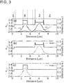
- the refractive index profile along the growth axis G is displayed in Fig. 3 (a) .
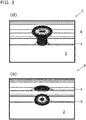
- the computed intensity profile of the antisymmetric (-) and symmetric (+) modes are also displayed, while the full two dimensional intensity profiles of these modes are reported in Fig. 3 (d) and (e) .
- the dispersion lines of the two uncoupled modes are reported in Fig. 3(f) , with dashed lines while the dispersion of the coupled modes are reported with full lines.
- Our simulation predicts a minimum of the GVD close to zero at the laser operation wavelength for the antisymmetric mode (-) (see Fig. 3(h) ) while the overlap with the active region is almost fully preserved (see Fig. 3 (g) ).
- the antisymmetric mode (-) has a much larger overlap with the active region ⁇ AR than the symmetric mode (+) which is localized in the passive core layer 4 / InGaAs waveguide. This induces a strong mode selection mechanism which ensures that the device operates with high efficiency on the low GVD antisymmetric mode (-).
- the proposed active region layer 3" is composed of a 643 nm thick layer Al 0.15 Ga 0.85 As. This is an example of a QD laser with a described waveguide heterostrucutre emitting at 1.3 ⁇ m.
- the vertical refractive index profile in the device along the growth axis G is displayed in Fig. 4 (a) .
- the computed intensity profile of the two fundamental TE modes are displayed as well (Mode (+) and Mode (-)).
- the full two dimensional intensity profiles of these modes are reported in Fig. 4 (d) and (e) .
- These two modes result from the coupling of the fundamental modes of the two distinct waveguides (Mode 1 and Mode 2).
- the refractive index and optical intensity profiles of the latest are reported in Fig. 4 (b) and (c) .
- the antisymmetric mode (-) has a higher overlap factor with the active region while the symmetric mode is localized primarily in the passive core layer 4" (GaAs waveguide) (+). In that case, mode selection results from the overlap with the active region which is larger for the antisymmetric mode (see Fig. 4 (g) ).
- Our model predicts a dispersion for the proposed waveguide close to zero GVD.
- MBE molecular beam epitaxy
- MOCVD metalorganic chemical vapour deposition
Landscapes
- Physics & Mathematics (AREA)
- Condensed Matter Physics & Semiconductors (AREA)
- General Physics & Mathematics (AREA)
- Electromagnetism (AREA)
- Optics & Photonics (AREA)
- Geometry (AREA)
- Semiconductor Lasers (AREA)
Abstract
A waveguide heterostructure (0) for a semiconductor laser with an active part (I), comprising an active region layer (3) depending of the type of semiconductor used, surrounded in direction of a growth axis (G) by at least an active part bottom cladding (30) and an active part top cladding (31), wherein the active part (I) is sandwiched between an electrode layer (1) and a substrate (2), usable for dispersion compensation in a semiconductor laser frequency comb setup, should be optimized in order to lower the group velocity dispersion in a broad spectral range. This is reached by introducing a passive part (II), comprising at least a intercladding layer (40) and a passive top cladding (41) surrounding a passive core layer (4) inserted into the sandwich between substrate (2) and electrode layer (1) in direction of a growth axis (G) on top or below the active part (I), wherein the intercladding layer (40), passive part top cladding (41) and passive core layer (4) are semiconductors and the refractive indices of active region layer (3, (n(3)) and passive core layer (4, (n(4)) are greater than refractive indices of intercladding layer (40, n(40)) and passive part top cladding (41, n(41)).
Description
- The present invention describes a waveguide heterostructure for a semiconductor laser with an active part, comprising an active region layer depending of the type of semiconductor used, which is sandwiched between an electrode layer and a substrate, usable for dispersion compensation in a semiconductor laser frequency comb setup, an optical frequency comb setup and a manufacturing method.
- The generation of optical frequency combs via direct electrical pumping of semiconductor lasers is considered an attractive alternative to the well established mode-locked laser sources that are Ti:sapphire or dye lasers in terms of compactness, robustness and integrability. However, the high chromatic dispersion of bulk semiconductor materials can prevent the propagation of frequency combs or lead to undesired pulse lengthening.
- In semiconductor laser frequency combs, in particular quantum cascade laser (QCL) frequency combs the mode-locking mechanism is the fourth wave mixing due to the high non-linearity of intersubband transitions. Efficient fourth wave mixing can only be obtained in frequency comb setups with quantum cascade lasers, if the group velocity dispersion inside the laser waveguide structure is sufficiently low. For interband lasers mode-locking is reached by the use of an integrated saturable absorber.
- According to prior art, for improvement of optical frequency comb operation, waveguide structures, comprising multi-layer dielectric coatings were deposited directly on the lasers back facets. The fabrication of high quality GTI coatings, working like Gires-Tournois-Interferometer (GTI), is challenging since due to the optical absorption of the materials used they overheat and burn. These are therefore incompatible with high optical output power and alternative solutions are required.
- Also Plasmon enhanced waveguides structures were optimized for low group velocity dispersion. But Plasmon enhanced waveguide structures cannot be used for low mid-infrared wavelengths due to the difficulty to increase the plasmon frequency accordingly.
- Quantum cascade laser based frequency comb sources have been demonstrated in the mid-infrared and terahertz spectral ranges. Dual comb spectroscopy setups based on these devices were demonstrated, showing their strong potential for the development of spectrometers based on broadband QCLs.
- At mid-infrared wavelengths the most efficient waveguides for QCLs are dielectric slab waveguide heterostructures. For the InGaAs/AlInAs material system, the active region is placed in between two InP layers, which act as bottom and top cladding layers. In the active region electrons are transformed to photons. Most of the time, thin layers of InGaAs are grown between the active region and the InP cladding layers in order to increase the refractive index contrast and therefore the optical confinement. Sometimes a low doped substrate is used as bottom cladding on which the active region is directly grown. For best performances, a low doped InP bottom cladding is grown on the InP substrate, before the growth of the active region. Finally, in order to lower losses due to the interaction with surface plasmon modes in the contact layer, a highly doped InP layer is usually grown on top of the top cladding. This waveguide heterostrucutre comprises an active region sandwiched in two cladding layer, wherein the sandwich lays between the substrate and an electrode layer. Such a waveguide heterostructure can be used in a frequency comb setup, but the reachable group velocity dispersion (GVD) inside the laser waveguide heterostructure could not be reduced to low enough values so far.
- In
US2014240509 a multiplicity of waveguide structures is disclosed and depicted, based on GaAs and AlGaAs. All presented waveguide structures have a layered form, comprising a substrate, a buffer layer, a first cladding layer, a core layer, a second cladding layer, a cap layer, an insulating layer and two electrodes. In the disclosed waveguide structures pulse compression is realized after the light has left the laser, wherein the means are not part of the laser cavity and therefore do not allow to realize compensation of the chromatic dispersion of the laser cavity. - The object of the present invention is to improve an optical frequency comb setup and a laser device, comprising a semiconductor laser with an optimized waveguide heterostructure, lowering the group velocity dispersion in a broad spectral range. An optical waveguide heterostructure of a semiconductor laser according to
claim 1 solves this problem. - Reachable semiconductor laser frequency comb setups according to the invention, based on the improved waveguide heterostructure have more spectral bandwidth and more optical output power, in comparison with prior art solutions.
- Moreover, it will secure exclusivity for short wavelengths (3-7µm) since no quantum cascade laser based frequency combs were available prior due to the high dispersion. Moreover, the use of the improved waveguide heterostructure can be used to reduce the dispersion of near-infrared mode-locked lasers and therefore lead to shortening of the pulse length in these devices.
- The optical waveguide heterostructure can be applied to different semiconductor lasers such as quantum well, quantum dash, quantum dot, interband cascade or quantum cascade lasers.
- Such semiconductor laser frequency comb setups can comprise different semiconductor lasers such as interband cascade lasers and quantum dot lasers. The disclosed solution is fully compatible with standard quantum cascade lasers fabrication processes used for commercially available laser devices.
- We have invented a novel wave guiding structure for semiconductor lasers which is able to compensate the group velocity dispersion in these devices and improve their performance as frequency combs. A secondary waveguide core is fabricated close to the standard active region primary core. Together, the two waveguides result in a coupled waveguide for which the fundamental mode dispersion can be tuned by varying the secondary core waveguide geometries and the distance between primary core and secondary core. The use of this effect makes possible heterostructures that have optimized group velocity dispersion for frequency comb operation in semiconductor lasers.
- The here presented semiconductor laser frequency comb setup will be used in an optical spectrometer.
The integration of coupled waveguides in the laser waveguide heterostructure is not trivial. - In such a structure two optical modes have identical losses and therefore reach threshold simultaneously. These are the antisymmetric mode which has negative GVD and the symmetric mode which has positive GVD.
The heterostructure here achieves mode selection on the antisymmetric and the antisymmetric mainly located in the active region waveguide core which allows to achieve laser operation with high performance. - Preferred exemplary embodiments of the subject matter of the invention are described below in conjunction with the attached drawings.
- Fig. 1
- shows a scheme of a waveguide heterostructure according to a first embodiment in form of a buried heterostructure quantum cascade laser (QCL).
- Fig. 2
- shows a scheme of a waveguide heterostructure according to a second embodiment in form of a ridge waveguide QD laser.
- Figures 3
- are showing
- (a)
- refractive index and mode intensity along the growth axis in an exemplary 4.6 µm QCL with waveguide structure according a first embodiment for the fundamental mode of the primary and secondary cores,
- (b)
- refractive index and mode intensity along the growth axis in an exemplary 4.6 µm QCL with waveguide heterostructure according to first embodiment without passive core layer/secondary core,
- (c)
- refractive index and mode intensity along the growth axis in an exemplary 4.6 µm QCL with waveguide heterostructure according to first embodiment without active region layer,
- (d)
- the 2D mode intensity of the fundamental mode of the passive core layer in an exemplary 4.6 µm QCL with waveguide heterostructure
- (e)
- the 2D and mode intensity of the fundamental mode of the active region layer in an exemplary 4.6 µm QCL with waveguide heterostructure
- (f)
- the effective refractive index dispersion of the optical modes
- (g)
- the overlap with active gain region ΓAR of the optical modes
- (h)
- the group velocity dispersion of the optical modes according to this first embodiment of the invention.
- Figures 4
- are showing a third embodiment of a waveguide heterostructure, wherein
- (a)
- shows a vertical cut plan of the intensity profile of Modes (-) and (+) and respective refractive index profile.
- (b)
- shows a vertical cut plan of the intensity profile of the mode for the active region core layer without the passive core layer (GaAs waveguide) and respective refractive index profile.
- (c)
- shows a vertical cut plan of the intensity profile of the mode for the passive core layer (GaAs waveguide) without the active region core layer and respective refractive index profile.
- (d)
- Intensity profile of Mode (-) at 8600 cm-1.
- (e)
- Intensity profile of Mode (+) at 8600 cm-1.
- (f)
- Spectrally resolved dispersion of the waveguides modes. The coupling of
Mode 1 andMode 2 results into the generation of two hybrid modes (-) and (+). - (g)
- Overlap factor with the active region core layer.
- (h)
- GVD of the modes. The induced GVD is positive for the upper branch mode (+) and negative for the lower branch Mode (-).
- We present different semiconductor laser, comprising an
optical waveguide heterostructure 0, 0' in different embodiments as part of semiconductor laser of different types.Such waveguide heterostructures 0, 0' can form part of laser devices for semiconductor laser frequency comb setups. Thewaveguide heterostructures 0, 0' have a layered setup, comprising different layer of different materials grown on asubstrate 2, 2' in direction of a growth axis G with a height and variable width, as depicted in the schematic cross section viewsFigure 1 and 2 . Thewaveguide heterostructure 0, 0' is a dual coupled waveguide for a semiconductor laser, comprising an active part I and a passive part II in a layered structure. The active part I comprises a claddedactive region layer 3, 3' and the passive part II comprises a claddedpassive core layer 4, 4' deposited onto another. Such awaveguide heterostructure 0, 0' is usable for dispersion compensation in semiconductor lasers. - Known semiconductor laser comprising quantum cascade laser (QCL) and quantum dot (QD) laser. In general quantum cascade laser are using an active part I/waveguide core with
active region layer 3 comprising quantum wells, the active region layer 3' of quantum dot lasers comprises quantum dots as active laser medium for light emission. - A first embodiment of
waveguide heterostructure 0 is based on anactive region layer 3, also named as primary core, of a buried heterostructure quantum cascade laser (QCL), wherein theactive region layer 3 is sandwiched between anelectrode layer 1 on one side and asubstrate 2 on the other side in direction of the growth axis G. All depicted layer are grown in direction of the growth axis G and are proceeding in longitudinal direction of thewaveguide heterostructure 0. In theactive region layer 3 of quantum cascade laser, the optical amplification takes place. Suchactive region layer 3 of quantum cascade laser are known to the person skilled in the art, in which laser emission in a repeated stack of semiconductor multiple quantum well heterostructures is achieved through, using intersubband transitions. There are setups known for forming superlattices in theactive region layer 3 of a QCL, to reach intersubband transitions and tune an emission wavelength. - The
active region layer 3 is in direction of the growth axis G surrounded by an activepart bottom cladding 30 and an activepart top cladding 31, building the active part I. Alateral regrowth layer 5 is surrounding the active part I withactive region layer 3 and surrounding active bottom andtop cladding active region layer 3 plane. On top of theactive region layer 3, above the active part top cladding 31 a passive part II, comprising apassive core layer 4, surrounded both-sided by at least anintercladding layer 40 and a passivetop cladding 41 is placed. Here additionalpassive part claddings top cladding 41, while an additionalpassive part cladding 44 is placed underneath theintercladding layer 40. Another lateral regrowth layer 5' is surrounding the passive part II withpassive core layer 4 and the surroundingpassive cladding layer passive core layer 4 plane. - The
electrode layer 1 covers the passive part II on the side facing away theactive region layer 3, while thesubstrate 2 is covering the active part I. The width wa of the active part I respectively of theactive region layer 3 can be smaller or larger than the width wp of the passive part II respectively thepassive core layer 4. As depicted infigure 1 wa is smaller than wp. - A distance d between the centre of the
active core layer 3 and the centre of thepassive core layer 4 is defined, lying at coupling distance, roughly between 100nm and 5 microns, in particular below 2000nm. - The
electrode layer 1 comprises a metal, in particular gold, while all other layers are made of semiconducting material with partly differing doping. We found an optimized waveguide heterostructure comprising the QCL active part I, InGaAs comprisingpassive core 4 and InP claddings and the substrate from InP as promising setup. - An example of a preferred detailed material mix of the
optical waveguide heterostructure 0 according to the first embodiment is depicted in table I andFigure 1 , showing a schematic vertical cross section of waveguide heterostructure for a 4.6 µm quantum cascade laser. This waveguide heterostructure is based on InGaAs/InP and a quantum cascade layer asactive region layer 3.Table I : Layer Material Thickness Doping metal electrode layer 1Metal/Au 0.3 µm additional passive part cladding 43InP 0.4 µm n=3e18 cm-3 additional passive part cladding 42InP 0.4 µm n=2e17 cm-3 passive top cladding 41InP 1.6 µm n=1e16 cm-3 passive core 4InGaAs 1.0 µ n=1e16 cm-3 passiv bottom cladding 40 (multiple layer) InP 1.2 µm n=1e16 cm-3 active part top cladding 31InGaAs 0.1 µm n=6e16 cm-3 active region of QCL 31.8 µm active part bottom cladding 30InGaAs 0.1 µm n=6e16 cm-3 substrate 2 InP Variable n=2e17 cm-3 substrate 2 and activepart bottom cladding 30. - All
cladding layer electrode layer 1 are semiconducting. - A second embodiment of a waveguide heterostructure 0' is based on an active region layer 3' of a ridge waveguide quantum dot (QD) laser. Also here the active region layer 3' is sandwiched between an
electrode layer 1 on one side and a substrate 2' on the other side in direction of a growth axis G. All depicted layers are grown in direction of the growth axis G and are proceeding in longitudinal direction of the waveguide heterostructure 0'. Quantum dots are arranged in the active region layer 3', in which the optical amplification takes place. Also different active region layer 3' of quantum dot lasers are known to the person skilled in the art. The active part I' is comprising an active part bottom cladding 30' and an active part top cladding 31' surrounding the active region 3' in direction of the growth axis G on two sides. Here a bottom cladding bc is arranged between the active part bottom cladding 30' and the substrate 2'. The bottom cladding bc is not a part of the active part I'. - Onto the active part I respectively onto the upper surface of the active part top cladding 31', facing away the substrate side of active region layer 3', the layered passive part II' is deposited. The passive part II' comprises a passive core layer 4' surrounded by a intercladding layer 40' and a passive
top cladding 41 on its both sides along the growth axis G. Here the passive core layer 4' width wp' is greater than the active layer 3' width wa'. The distance d' between the centres of the active region layer 3' and the passive core layer 4' is depicted, lying at coupling distance. - The schematic vertical cross section according to
Figure 2 shows the second embodiment of a waveguide heterostructure 0', based on GaAs/AlxGayAs for passive core layer 4' and cladding layer 30', 31', 40', 41', with a known quantum dot layer as active region layer 3'. An example of a preferred detailed material mix of the optical waveguide heterostructure 0' according to the second embodiment is depicted in table II andFigure 2 .Table II: Layer Material Thickness Doping metal electrode layer 1Au 0.3 µm passive top cladding 41' Al0.35Ga0.65As 0.76µm n=1e17 cm-3 passive core layer 4' GaAs 0.6µm n=1e17 cm-3 intercladding layer 40' Al0.35Ga0.65As 0.56 µm n=1e17 cm-3 active part top cladding 31' Al0.15Ga0.85AS 0.3 µm n=1e17 cm-3 active region layer (QD) 3' 0.07 µm active part bottom cladding 30' Al0.15Ga0.85AS 0.3 µm p=1e18 cm-3 bottom cladding bc Al0.35Ga0.65As 1.52 µm p=1e18 cm-3 Substrate 2' GaAs p=1e18 cm-3 - All cladding layer 30', 31', bc, 40', 41' are optical passive cladding layer, independent, if they belong to the active part I or passive part II. As shown in table II, all layers, other than the
electrode layer 1 are semiconducting with variable doping. - In all embodiments in the
active part 3, 3', respectively theactive region layer 3, 3' optical amplification takes place. Possibleactive region layer 3, 3' are quantum cascade structures, an interband cascade structure, a quantum well structure, a quantum dash structure, a quantum dot structure or any other possible structure providing gain in semiconductor lasers. Thepassive core layer 4, 4' is a layer which confines light and provides neither significant gain or losses. Thewaveguide heterostructure 0, 0' have to comprise oneactive region layer 3, 3' (primary core region), at least onepassive core layer 4, 4' (secondary core region) and the cladding. By tuning the coupling strength of the two optical modes located in each separated core, their dispersion slope can be modulated. - The
passive core layer 4, 4' geometries and position relative to theactive region layer 3, 3' in direction of the growth axis G can be tuned in order to optimize the group velocity dispersion of the fundamental mode of theactive region layer 3, 3'. - A semiconductor laser with
novel waveguide heterostructure 0, 0' provides an optimized group velocity dispersion for frequency comb operation. - In General the width wa, wa' and wp, wp' can have a value between the wavelength of the laser up to 15 times the wavelength of the laser.
- Typical distances d, d' are at a coupling distance, from 100 nm up to 1.5 times the wavelength of the laser, roughly between 100nm and 5 microns, in particular below 2000nm.
Although the passive part II is here as depicted always located in growth direction G above the active part I the other orientation is also possible. - Concerning refractive indices of the different layer, examples are depicted in
Figure 3 and4 .
In a QCL setup grown on InP the refractive index of the substrate 2 n(2) is less than the refractive index of active region layer 3 (n(3)), passive core layer 4 (n(4)), and refractive indices of active part bottom cladding 30 (n(30)) and active part top cladding 31 (n(31)).
In a QD setup, grown on GaAs, thesubstrate 2 has a high refractive index and the use of a cladding is mandatory. - The refractive indices of active region layer 3 (n(3)), passive core layer 4 (n(4)), and refractive indices of active part bottom cladding 30 (n(30)) and active part top cladding 31 (n(31)) are greater than the refractive indices of intercladding layer 40 (n(40)), passive part top cladding 41 (n(41)) and the additional
passive part claddings - In case the bottom cladding bc is used, the associated refractive index n(bc) is less than the refractive indices n(3), n(4), n(30) and n(31).
- Optionally the refractive index of
active region layer 3 can be smaller than the refractive index of thepassive core layer 4. - We simulated the optical modes for various geometries using a finite element solver and targeted zero GVD at the central wavelength. The structure optimized for low GVD at 4.6 µm is detailed in Table I. This is an example of a QCL with a described waveguide heterostrucutre emitting at 4.6 µm.
- The
active region layer 3 width is 4 µm and thepassive core layer 4 / InGaAs secondary waveguide width is 6.7 µm. - The refractive index profile along the growth axis G is displayed in
Fig. 3 (a) . The computed intensity profile of the antisymmetric (-) and symmetric (+) modes are also displayed, while the full two dimensional intensity profiles of these modes are reported inFig. 3 (d) and (e) . These two modes result from the coupling of the fundamental modes (Mode 1 and Mode 2) of the two distinct waveguides with GVD D1= 1140 fs2/mm andD 2= 2600 fs2/mm. - The dispersion lines of the two uncoupled modes are reported in
Fig. 3(f) , with dashed lines while the dispersion of the coupled modes are reported with full lines.
Our simulation predicts a minimum of the GVD close to zero at the laser operation wavelength for the antisymmetric mode (-) (seeFig. 3(h) ) while the overlap with the active region is almost fully preserved (seeFig. 3 (g) ). In turn, the antisymmetric mode (-) has a much larger overlap with the active region ΓAR than the symmetric mode (+) which is localized in thepassive core layer 4 / InGaAs waveguide. This induces a strong mode selection mechanism which ensures that the device operates with high efficiency on the low GVD antisymmetric mode (-). - We propose
anoptical waveguide heterostructure 0", in form of a dual waveguide for GaAs/AlGaAs quantum dot lasers. The proposedactive region layer 3" is composed of a 643 nm thick layer Al0.15Ga0.85As. This is an example of a QD laser with a described waveguide heterostrucutre emitting at 1.3 µm. - The
active region layer 3" (core waveguide) is placed in between two Al0.35Ga0.25 1520 nm cladding layers (Si doped n=10 17 cm-3 and C doped p=10 18 cm-3) 30", 31". - A 360 nm
passive core layer 4" (GaAs waveguide) is placed in theupper cladding layer 41" at a distance d=700 nm to theactive region layer 3" (primary core waveguide). - The vertical refractive index profile in the device along the growth axis G is displayed in
Fig. 4 (a) . The computed intensity profile of the two fundamental TE modes are displayed as well (Mode (+) and Mode (-)). The full two dimensional intensity profiles of these modes are reported inFig. 4 (d) and (e) . These two modes result from the coupling of the fundamental modes of the two distinct waveguides (Mode 1 and Mode 2). The refractive index and optical intensity profiles of the latest are reported inFig. 4 (b) and (c) . - In
Fig. 4 (f) , the dispersion lines of the two uncoupled modes (Mode 1 and Mode 2) are reported with dashed lines while the dispersion of the coupled modes are reported with full lines. - Since
passive core layer 4" (GaAs) has a refractive index larger than the refractive index of theactive region layer 3", the antisymmetric mode (-) has a higher overlap factor with the active region while the symmetric mode is localized primarily in thepassive core layer 4" (GaAs waveguide) (+). In that case, mode selection results from the overlap with the active region which is larger for the antisymmetric mode (seeFig. 4 (g) ). Our model predicts a dispersion for the proposed waveguide close to zero GVD. - For production of the waveguide heterostructures molecular beam epitaxy (MBE) and/or metalorganic chemical vapour deposition (MOCVD) can be used. A subsequent deposition of the layers onto the
substrate 2 is carried out, depending ofwaveguide heterostructure embodiment -
- 0, 0' optical waveguide heterostructure (semiconductor)
- 1 electrode layer (metal)
- 2 substrate (semiconductor)
- I active part
- 3 active region layer/primary core/QC layer / QD layer
- 30 active part bottom cladding
- 31 active part top cladding
- wa width
- II passive part
- 4 passive core layer
- 40 intercladding layer
- 41 passive part top cladding
- 42, 43, 44 additional passive part cladding
- wp width
- d, d' distance in direction of growth axis between 3 and 4
- bc bottom cladding
- 5, 5' lateral regrowth layer
Claims (17)
- A waveguide heterostructure (0, 0', 0") for a semiconductor laser with an active part (I), comprising an active region layer (3, 3') depending of the type of semiconductor used, which is sandwiched between an electrode layer (1) and a substrate (2), usable for dispersion compensation in a semiconductor laser frequency comb setup,
characterized in that
a passive part (II), comprising at least an intercladding layer (40) and a passive part top cladding (41) surrounding a passive core layer (4) is inserted into the sandwich between substrate (2) and electrode layer (1) in direction of a growth axis (G) on top or below the active part (I), wherein the intercladding layer (40), passive part top cladding (41) and passive core layer (4) are semiconductors and the refractive indices of active region layer (3, (n(3)) and passive core layer (4, (n(4)) are greater than refractive indices of intercladding layer (40, n(40)) and passive part top cladding (41, n(41)). - Waveguide heterostructure (0, 0', 0") according to claim 1, wherein the active region layer (3, 3') is surrounded by an active part bottom cladding (30, 30', n(30)) and an active part top cladding (31, 31', n(31)), wherein the refractive indices of the active claddings (30, 30', 31, 31') are greater than refractive indices of intercladding layer (40, n(40)) and passive part top cladding (41, n(41)).
- Waveguide heterostructure (0, 0', 0") according to one of the preceding claims, wherein the active region layer (3) is build of a quantum cascade structure, an interband cascade structure, a quantum well structure, a quantum dash structure, a quantum dot structure or any other possible structure providing gain in semiconductor lasers.
- Waveguide heterostructure (0, 0', 0") according to one of the claims 1 to 2, wherein the active region layer (3) is build of an active layer of a quantum cascade laser (QCL).
- Waveguide heterostructure (0, 0', 0") according to claim 4, wherein on top of the passive top cladding (41) in direction of the growth axis (G), averted the passive core layer (4), at least one additional passive part cladding (42, 43) is deposited, while at least one additional passive part cladding (44) is placed underneath the intercladding layer (40), directly onto the active part top cladding (31).
- Waveguide heterostructure (0, 0', 0") according to one of the preceding claims, wherein the width (wa) of the active region layer (3) is smaller than the width (wp) of the passive core layer (4) in direction perpendicular to the growth axis (G).
- Waveguide heterostructure (0, 0', 0") according to one of the preceding claims, wherein lateral regrowth layer (5, 5') surrounding the active part (I) laterally parallel to the active region layer (3) plane and surrounding the passive part (II) laterally parallel to the passive core layer (4) are stacked.
- Waveguide heterostructure (0, 0', 0") according to one of the claims 1 to 7, wherein the composition of the waveguide heterostructure (0) is chosen according to:
Layer Material passive top cladding 41 InP passive core 4 InGaAs passiv bottom cladding 40 InP active part top cladding 31 InGaAs active part bottom cladding 30 InGaAs substrate 2 InP - Waveguide heterostructure (0, 0', 0") according to claim 8, wherein the additional cladding layer (42, 43) are comprising doped Indium phosphide (InP).
- Waveguide heterostructure (0') according to one of the claims 1 to 2, wherein the active region layer (3') is build of an active layer of a ridge waveguide quantum dot (QD) laser.
- Waveguide heterostructure (0') according to claim 10, wherein between the substrate (2') and the active part bottom cladding (30'), averted the passive core layer (4), an bottom cladding (bc) is deposited, wherein the associated refractive index n(bc) is less than the refractive indices n(3), n(4), n(30) and n(31).
- Waveguide heterostructure (0') according to claim 10 or 11, wherein the width (wa') of the active part (I) is greater than the width (wp') of the passive part (II).
- Waveguide heterostructure (0') according to one of the claims 10 to 12, wherein the height of the active region layer (3') is less than half the height of the passive core layer (4').
- Waveguide heterostructure (0') according to one of the claims 10 to 13, wherein the composition of the waveguide heterostructure (0') is chosen according to:
Layer Material passive top cladding 41' Al0.35Ga0.65As passive core layer 4' GaAs intercladding layer 40' Al0.35Ga0.65As active part top cladding 31' Al0.15Ga0.85AS active region layer (QD) 3' active part bottom cladding 30' Al0.15Ga0.85AS bottom cladding bc Al0.35Ga0.65As Substrate 2' GaAs - Waveguide heterostructure (0, 0', 0") according to one of the preceding claims, wherein the distance (d) between the centres of the active region layer (3, 3', 3") and the passive core layer (4, 4', 4") lies between 100nm and 5 micron, in particular below 2000nm.
- Semiconductor laser frequency comb setup, comprising at least one semiconductor laser with a waveguide heterostructure (0, 0', 0") according to one of the claims 1 to 15.
- Manufacturing method of an optical waveguide heterostructure (0, 0', 0") according to one of the claims 1 to 15, characterized by the steps:- providing a waveguide heterostructure (0, 0', 0") for a semiconductor laser with a semiconductor substrate (2) on which an active part (I), comprising an active region layer (3, 3') depending of the type of semiconductor used, surrounded in direction of a growth axis (G) by at least an active part bottom cladding (30, 30') and an active part top cladding (31, 31'), is deposited,- subsequently depositing a passive part (II), comprising at least a intercladding layer (40), a passive core layer (4) and at least a passive top cladding (41) in growth axis (G) direction, before- an electrode layer (1) is deposited onto the dual active part (I) passive part (II) sandwich.
Priority Applications (4)
| Application Number | Priority Date | Filing Date | Title |
|---|---|---|---|
| EP17194352.5A EP3462554A1 (en) | 2017-10-02 | 2017-10-02 | Waveguide heterostructure for dispersion compensation in semiconductor laser |
| US16/652,514 US11070030B2 (en) | 2017-10-02 | 2018-09-27 | Waveguide heterostructure for dispersion compensation in semiconductor laser |
| PCT/EP2018/076281 WO2019068554A1 (en) | 2017-10-02 | 2018-09-27 | Waveguide heterostructure for dispersion compensation in semiconductor laser |
| EP18778914.4A EP3692609B1 (en) | 2017-10-02 | 2018-09-27 | Waveguide heterostructure for dispersion compensation in semiconductor laser |
Applications Claiming Priority (1)
| Application Number | Priority Date | Filing Date | Title |
|---|---|---|---|
| EP17194352.5A EP3462554A1 (en) | 2017-10-02 | 2017-10-02 | Waveguide heterostructure for dispersion compensation in semiconductor laser |
Publications (1)
| Publication Number | Publication Date |
|---|---|
| EP3462554A1 true EP3462554A1 (en) | 2019-04-03 |
Family
ID=60001777
Family Applications (2)
| Application Number | Title | Priority Date | Filing Date |
|---|---|---|---|
| EP17194352.5A Withdrawn EP3462554A1 (en) | 2017-10-02 | 2017-10-02 | Waveguide heterostructure for dispersion compensation in semiconductor laser |
| EP18778914.4A Active EP3692609B1 (en) | 2017-10-02 | 2018-09-27 | Waveguide heterostructure for dispersion compensation in semiconductor laser |
Family Applications After (1)
| Application Number | Title | Priority Date | Filing Date |
|---|---|---|---|
| EP18778914.4A Active EP3692609B1 (en) | 2017-10-02 | 2018-09-27 | Waveguide heterostructure for dispersion compensation in semiconductor laser |
Country Status (3)
| Country | Link |
|---|---|
| US (1) | US11070030B2 (en) |
| EP (2) | EP3462554A1 (en) |
| WO (1) | WO2019068554A1 (en) |
Families Citing this family (3)
| Publication number | Priority date | Publication date | Assignee | Title |
|---|---|---|---|---|
| GB2598144A (en) | 2020-08-21 | 2022-02-23 | Eth Zuerich | Cascade lasers |
| US20220344902A1 (en) * | 2021-04-22 | 2022-10-27 | Intraband LLC | Semiconductor Laser Structure for Higher-Order Mode Suppression |
| CN119137821A (en) | 2022-03-08 | 2024-12-13 | 阿尔佩斯激光有限公司 | Quantum cascade laser optical frequency comb |
Citations (4)
| Publication number | Priority date | Publication date | Assignee | Title |
|---|---|---|---|---|
| US20060056477A1 (en) * | 2004-01-16 | 2006-03-16 | Lammert Robert M | Laser diode with a frequency converter |
| US8780949B2 (en) * | 2012-06-25 | 2014-07-15 | Mitsubishi Electric Corporation | Optical semiconductor device |
| US20140240509A1 (en) | 2013-02-27 | 2014-08-28 | Seiko Epson Coporation | Short light pulse generation device, terahertz wave generation device, camera, imaging device, and measurement device |
| US20160156153A1 (en) * | 2014-10-21 | 2016-06-02 | Board Of Regents, The University Of Texas System | Generating Terahertz Frequency Combs from Quantum Cascade Lasers using Nonlinear Frequency Mixing |
Family Cites Families (3)
| Publication number | Priority date | Publication date | Assignee | Title |
|---|---|---|---|---|
| US6849866B2 (en) * | 1996-10-16 | 2005-02-01 | The University Of Connecticut | High performance optoelectronic and electronic inversion channel quantum well devices suitable for monolithic integration |
| US7776753B2 (en) * | 2002-10-25 | 2010-08-17 | University Of Connecticut | Method of fabricating semiconductor devices employing at least one modulation doped quantum well structure and one or more etch stop layers for accurate contact formation |
| US7015120B2 (en) * | 2002-10-25 | 2006-03-21 | The University Of Connecticut | Method of fabricating semiconductor devices employing at least one modulation doped quantum well structure and one or more etch stop layers for accurate contact formation |
-
2017
- 2017-10-02 EP EP17194352.5A patent/EP3462554A1/en not_active Withdrawn
-
2018
- 2018-09-27 WO PCT/EP2018/076281 patent/WO2019068554A1/en not_active Ceased
- 2018-09-27 US US16/652,514 patent/US11070030B2/en active Active
- 2018-09-27 EP EP18778914.4A patent/EP3692609B1/en active Active
Patent Citations (4)
| Publication number | Priority date | Publication date | Assignee | Title |
|---|---|---|---|---|
| US20060056477A1 (en) * | 2004-01-16 | 2006-03-16 | Lammert Robert M | Laser diode with a frequency converter |
| US8780949B2 (en) * | 2012-06-25 | 2014-07-15 | Mitsubishi Electric Corporation | Optical semiconductor device |
| US20140240509A1 (en) | 2013-02-27 | 2014-08-28 | Seiko Epson Coporation | Short light pulse generation device, terahertz wave generation device, camera, imaging device, and measurement device |
| US20160156153A1 (en) * | 2014-10-21 | 2016-06-02 | Board Of Regents, The University Of Texas System | Generating Terahertz Frequency Combs from Quantum Cascade Lasers using Nonlinear Frequency Mixing |
Also Published As
| Publication number | Publication date |
|---|---|
| EP3692609A1 (en) | 2020-08-12 |
| WO2019068554A1 (en) | 2019-04-11 |
| US20200287353A1 (en) | 2020-09-10 |
| EP3692609B1 (en) | 2023-12-27 |
| US11070030B2 (en) | 2021-07-20 |
Similar Documents
| Publication | Publication Date | Title |
|---|---|---|
| EP2957004B1 (en) | Single-step-grown transversely coupled distributed feedback laser | |
| US6717971B2 (en) | Semiconductor lasers | |
| US8319229B2 (en) | Optical semiconductor device and method for manufacturing the same | |
| US8855156B2 (en) | DFB laser diode having a lateral coupling for large output power | |
| KR101133380B1 (en) | Surface emitting laser | |
| US9407065B2 (en) | Semiconductor laser | |
| EP1717919A2 (en) | Semiconductor laser and method of fabricating the same | |
| US9698570B2 (en) | Optical semiconductor element and method of manufacturing the same | |
| JP5698267B2 (en) | Semiconductor device | |
| US8304757B2 (en) | Semiconductor light-emitting device, optical module, transmitter, and optical communication system | |
| US11070030B2 (en) | Waveguide heterostructure for dispersion compensation in semiconductor laser | |
| JP2014509084A (en) | Multistage quantum cascade laser with p-type isolation region | |
| JPH08279650A (en) | Semiconductor laser device and method of manufacturing semiconductor laser device | |
| WO2023154719A2 (en) | Weak index guiding of interband cascade lasers bonded to gaas substrates | |
| CN120500167A (en) | Three-section integrated high-power super-radiation light-emitting diode and preparation method thereof | |
| JP2009260093A (en) | Optical semiconductor device | |
| CN116544781B (en) | A semiconductor mode-locked laser and its fabrication method | |
| US20070153856A1 (en) | Semiconductor laser device | |
| US20260058442A1 (en) | Quantum Cascade Lasers With Narrow Core Ridge Waveguide Design | |
| JP7541725B2 (en) | Semiconductor laser element and epitaxial substrate | |
| US20220344902A1 (en) | Semiconductor Laser Structure for Higher-Order Mode Suppression | |
| JP2026065538A (en) | Semiconductor laser element | |
| JP2001144372A (en) | Semiconductor laser device | |
| JP2005317659A (en) | Integrated semiconductor optical device and its manufacturing method | |
| JP2003060312A (en) | Semiconductor laser element |
Legal Events
| Date | Code | Title | Description |
|---|---|---|---|
| PUAI | Public reference made under article 153(3) epc to a published international application that has entered the european phase |
Free format text: ORIGINAL CODE: 0009012 |
|
| AK | Designated contracting states |
Kind code of ref document: A1 Designated state(s): AL AT BE BG CH CY CZ DE DK EE ES FI FR GB GR HR HU IE IS IT LI LT LU LV MC MK MT NL NO PL PT RO RS SE SI SK SM TR |
|
| AX | Request for extension of the european patent |
Extension state: BA ME |
|
| STAA | Information on the status of an ep patent application or granted ep patent |
Free format text: STATUS: THE APPLICATION IS DEEMED TO BE WITHDRAWN |
|
| 18D | Application deemed to be withdrawn |
Effective date: 20191005 |