EP3462541A1 - Antenna circuit - Google Patents
Antenna circuit Download PDFInfo
- Publication number
- EP3462541A1 EP3462541A1 EP18800462.6A EP18800462A EP3462541A1 EP 3462541 A1 EP3462541 A1 EP 3462541A1 EP 18800462 A EP18800462 A EP 18800462A EP 3462541 A1 EP3462541 A1 EP 3462541A1
- Authority
- EP
- European Patent Office
- Prior art keywords
- antenna
- currents
- antennas
- amplitude ratio
- phase difference
- Prior art date
- Legal status (The legal status is an assumption and is not a legal conclusion. Google has not performed a legal analysis and makes no representation as to the accuracy of the status listed.)
- Granted
Links
Images


Classifications
-
- H—ELECTRICITY
- H04—ELECTRIC COMMUNICATION TECHNIQUE
- H04B—TRANSMISSION
- H04B5/00—Near-field transmission systems, e.g. inductive or capacitive transmission systems
- H04B5/20—Near-field transmission systems, e.g. inductive or capacitive transmission systems characterised by the transmission technique; characterised by the transmission medium
- H04B5/24—Inductive coupling
- H04B5/26—Inductive coupling using coils
-
- H—ELECTRICITY
- H01—ELECTRIC ELEMENTS
- H01Q—ANTENNAS, i.e. RADIO AERIALS
- H01Q7/00—Loop antennas with a substantially uniform current distribution around the loop and having a directional radiation pattern in a plane perpendicular to the plane of the loop
- H01Q7/005—Loop antennas with a substantially uniform current distribution around the loop and having a directional radiation pattern in a plane perpendicular to the plane of the loop with variable reactance for tuning the antenna
-
- H—ELECTRICITY
- H01—ELECTRIC ELEMENTS
- H01Q—ANTENNAS, i.e. RADIO AERIALS
- H01Q1/00—Details of, or arrangements associated with, antennas
- H01Q1/50—Structural association of antennas with earthing switches, lead-in devices or lightning protectors
-
- H—ELECTRICITY
- H01—ELECTRIC ELEMENTS
- H01Q—ANTENNAS, i.e. RADIO AERIALS
- H01Q21/00—Antenna arrays or systems
- H01Q21/06—Arrays of individually energised antenna units similarly polarised and spaced apart
- H01Q21/08—Arrays of individually energised antenna units similarly polarised and spaced apart the units being spaced along or adjacent to a rectilinear path
-
- H—ELECTRICITY
- H01—ELECTRIC ELEMENTS
- H01Q—ANTENNAS, i.e. RADIO AERIALS
- H01Q5/00—Arrangements for simultaneous operation of antennas on two or more different wavebands, e.g. dual-band or multi-band arrangements
- H01Q5/30—Arrangements for providing operation on different wavebands
- H01Q5/307—Individual or coupled radiating elements, each element being fed in an unspecified way
- H01Q5/314—Individual or coupled radiating elements, each element being fed in an unspecified way using frequency dependent circuits or components, e.g. trap circuits or capacitors
- H01Q5/335—Individual or coupled radiating elements, each element being fed in an unspecified way using frequency dependent circuits or components, e.g. trap circuits or capacitors at the feed, e.g. for impedance matching
-
- H—ELECTRICITY
- H01—ELECTRIC ELEMENTS
- H01Q—ANTENNAS, i.e. RADIO AERIALS
- H01Q7/00—Loop antennas with a substantially uniform current distribution around the loop and having a directional radiation pattern in a plane perpendicular to the plane of the loop
-
- H—ELECTRICITY
- H04—ELECTRIC COMMUNICATION TECHNIQUE
- H04B—TRANSMISSION
- H04B5/00—Near-field transmission systems, e.g. inductive or capacitive transmission systems
- H04B5/40—Near-field transmission systems, e.g. inductive or capacitive transmission systems characterised by components specially adapted for near-field transmission
- H04B5/43—Antennas
Definitions
- the present invention relates to a wireless communication technology that enables desired setting of a boundary of a communication area.
- a system using a magnetic field has been in practical use as such a wireless communication system.
- a loop antenna and a bar antenna have been used for generating the magnetic field.
- a disclosed effective way in generating a magnetic field desired by a designer is to use multiple antennas and appropriately control phases of currents flowing through those antennas (Patent document 1).
- the technology using multiple antennas usually employs a configuration in which the multiple antennas are connected in series (Patent document 2).
- Such a series connection configuration requires only one signal source, which is an advantage.
- amplitude and phases of currents flowing through the antennas naturally take the same values in all the antennas.
- the present invention is made in light of the above-described problem, and has an object to control the amplitude and phases of the currents flowing through the multiple antennas connected in series into desired values.
- An antenna circuit includes: a first antenna; a second antenna that is connected in series with the first antenna and includes inductance; an adjustment capacitor that is connected in parallel with the second antenna; and an adjustment resistor that is connected in parallel with the second antenna.
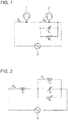
- Fig. 1 is a diagram that illustrates a configuration example of an antenna circuit of this embodiment.
- the antenna circuit illustrated in Fig 1 includes multiple antennas 1 and 2 connected in series, a signal source 3, and a variable capacitor C v and a variable resistor R v connected in parallel with the antenna 2.
- the antennas 1 and 2 are connected such that currents therethrough flow in different directions from each other. However, the antennas 1 and 2 may be connected such that the currents therethrough flow in the same direction.
- Complex amplitude of a current I 2 flowing through the antenna 2 varies according to a capacitance value of the variable capacitor C v and a resistance value of the variable resistor R v and differs from complex amplitude of a current I 1 flowing through the antenna 1.
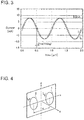
- Fig. 2 illustrates an equivalent circuit of the antenna circuit in Fig. 1 .
- Z 1 represents impedance of the antenna 1.
- L 2 represents inductance of the antenna 2.
- ⁇ is an angular frequency of a signal generated by the signal source 3.
- the antenna 2 may be at least an antenna having inductance such as a loop antenna and a bar antenna.
- the antennas 1 and 2 have the same shape; however, they may have different shapes.
- the desired actual amplitude ratio r 0 and phase difference ⁇ 0 can be achieved by setting the value of the variable capacitor C v of the antenna circuit in Fig. 1 to a value obtained from the equation (3) and setting the value of the variable resistor R v of the antenna circuit in Fig. 1 to a value obtained from the equation (4).
- a signal frequency f of the signal source 3 and the inductance L 2 of the antenna 2 are values of the following equation (6).
- f 1 MHz
- L 2 10 ⁇ ⁇ ⁇ H
- Fig. 3 illustrates waveforms of the currents I 1 and I 2 in a simulation on the equivalent circuit in Fig. 2 using the parameters of the equations (6) and (7).
- An amplitude of voltage applied from the signal source 3 is 1V.
- Fig. 3 it can be seen that the amplitude ratio between the currents I 1 and I 2 is 1 and a time difference therebetween is 31 ns (comparable to 11 deg).
- employment of the values C v opt and R v opt calculated from the equations (3) and (4) enables controlling of the amplitude ratio and phase difference between the currents I 1 and I 2 flowing through the antennas 1 and 2 as desired.
- the antennas 1 and 2 having the same shape are disposed in an x-y plane. It is assumed that directions of the currents I 1 and I 2 flowing through the antennas 1 and 2 are different from each other.
- Fig. 5 is a diagram that illustrates magnetic field distribution obtained when currents with the amplitude ratio of 1 and no phase difference are applied to the antennas 1 and 2 illustrated in Fig. 4 .
- Fig. 6 is a diagram that illustrates magnetic field distribution obtained when the currents I 1 and I 2 illustrated in Fig. 3 are applied to the antennas 1 and 2 illustrated in Fig. 4 .
- Each contour in Figs. 5 and 6 indicate a line plotting points where a magnetic field strength has a certain value at a y-coordinate of 0, 50, 60, 70, or 80 cm.
- the contour is divided when a value of the y-coordinate is large, and this is a problem in forming a communication area.
- the contour is not divided even when the value of the y-coordinate is large, and this enables forming of a favorable communication area.
- the magnetic field distribution obtained by the conventional antenna circuit configuration is symmetric about a y-z plane.
- changing of only phases of the currents I 1 and I 2 flowing through the antennas 1 and 2 still makes the magnetic field distribution symmetric about the y-z plane.
- asymmetric magnetic field distribution may be desired in some application.
- Fig. 7 illustrates waveforms of the currents I 1 and I 2 in a simulation on the equivalent circuit in Fig. 2 using the parameters of the equations (6) and (9).
- An amplitude of voltage applied from the signal source 3 is 1V.
- Fig. 7 it can be seen that the amplitude ratio of the currents I 1 and I 2 is 1/1.3 and a time difference therebetween is 28 ns (comparable to 10 deg).
- Fig. 8 is a diagram that illustrates magnetic field distribution obtained when the currents I 1 and I 2 illustrated in Fig. 7 are applied to the antennas 1 and 2 illustrated in Fig. 4 . As illustrated in Fig. 8 , it can be seen that magnetic field distribution asymmetric about the y-z plane is formed.
- Fig. 9 is a diagram that illustrates a configuration example of the other antenna circuit of this embodiment.
- the antenna circuit illustrated in Fig. 9 is different from the antenna circuit in Fig. 1 in that a resistor R 1 and a capacitor C 1 as well as a resistor R 2 and a capacitor C 2 are connected in series with the antenna 1 and the antenna 2 respectively.
- the variable capacitor C v and the variable resistor R v are connected in parallel with the components including the antenna 2, the resistor R 2 , and the capacitor C 2 .
- a capacitor is connected in series with the antenna in order to reduce the impedance due to the inductance of the loop antenna.
- a resistor is intentionally connected in order to decrease a quality factor of the antenna.
- Fig. 10 illustrates an equivalent circuit of the antenna circuit in Fig. 9 .
- the capacitance value C v opt of the variable capacitor C v and the resistance value R v opt of the variable resistor R v for achieving the desired actual amplitude ratio r 0 and phase difference ⁇ 0 between the currents can be obtained from the following equations (10) and (11).
- C v opt C 2 ⁇ ⁇ C 2 R 2 r 0 sin ⁇ 0 + ⁇ 2 L 2 C 2 ⁇ 1 1 ⁇ r 0 cos ⁇ 0 1 + ⁇ C 2 R 2 2 + ⁇ 2 L 2 C 2 ⁇ 2 L 2 C 2 ⁇ 2 [Math.
- R v opt 1 ⁇ C 2 1 + ⁇ C 2 R 2 2 + ⁇ 2 L 2 C 2 ⁇ 2 L 2 C 2 ⁇ 2 ⁇ C 2 R 2 r 0 cos ⁇ 0 ⁇ 1 + r 0 sin ⁇ 0 ⁇ 2 L 2 C 2 ⁇ 1
- Fig. 11 illustrates waveforms of the currents I 1 and I 2 in a simulation on the equivalent circuit in Fig. 10 using the parameters of the equations (13) and (14).
- An amplitude of voltage applied from the signal source 3 is 1V.
- Fig. 11 it can be seen that the amplitude ratio of the currents I 1 and I 2 is 1 and a time difference therebetween is 31 ns (comparable to 11 deg).
- the amplitude of the currents I 1 and I 2 is greater than that in Fig. 3 .
- Fig. 12 illustrates waveforms of the currents I 1 and I 2 in a simulation on the equivalent circuit in Fig. 10 using the parameters of the equations (13) and (16).
- An amplitude of voltage applied from the signal source 3 is 1V.
- Fig. 12 it can be seen that the amplitude ratio of the currents I 1 and I 2 is 1.3 and a time difference therebetween is 31 ns (comparable to 11 deg).
- the amplitude of the currents I 1 and I 2 is greater than that in Fig. 7 .
- the variable capacitor C v and the variable resistor R v connected in parallel with the antenna 2 are provided, and this enables controlling of the actual amplitude ratio r and the phase difference ⁇ between the currents I 1 and I 2 flowing through the two antennas 1 and 2 into desired values. Flows of the currents I 1 and I 2 with the phase difference ⁇ through the antennas 1 and 2 enables forming of a favorable communication area. In addition, setting of the actual amplitude ratio r between the currents I 1 and I 2 flowing through the antennas 1 and 2 to a value other than 1 enables forming of an asymmetric communication area.
Landscapes
- Engineering & Computer Science (AREA)
- Computer Networks & Wireless Communication (AREA)
- Signal Processing (AREA)
- Variable-Direction Aerials And Aerial Arrays (AREA)
Abstract
Description
- The present invention relates to a wireless communication technology that enables desired setting of a boundary of a communication area.
- The needs of a wireless communication system that limits a communication area as desired have been increased recently. A system using a magnetic field has been in practical use as such a wireless communication system. A loop antenna and a bar antenna have been used for generating the magnetic field. A disclosed effective way in generating a magnetic field desired by a designer is to use multiple antennas and appropriately control phases of currents flowing through those antennas (Patent document 1).
-
- Patent document 1: Japanese Patent No.
6059833 - Patent document 2: Japanese Patent No.
6069548 - In general, the technology using multiple antennas usually employs a configuration in which the multiple antennas are connected in series (Patent document 2). Such a series connection configuration requires only one signal source, which is an advantage. However, in the simple series connection configuration disclosed in
Patent document 2, amplitude and phases of currents flowing through the antennas naturally take the same values in all the antennas. - Thus, there is a problem that multiple signal sources are needed in order to control the amplitude and phases of the currents flowing through the antennas according to the proposition of
Patent document 1. - The present invention is made in light of the above-described problem, and has an object to control the amplitude and phases of the currents flowing through the multiple antennas connected in series into desired values.
- An antenna circuit according to an aspect of the present invention includes: a first antenna; a second antenna that is connected in series with the first antenna and includes inductance; an adjustment capacitor that is connected in parallel with the second antenna; and an adjustment resistor that is connected in parallel with the second antenna.
- According to the present invention, it is possible to control amplitude and phases of currents flowing through multiple antennas connected in series into desired values.
-
-
Fig. 1 is a diagram that illustrates a configuration example of an antenna circuit of an embodiment. -
Fig. 2 is a diagram that illustrates an equivalent circuit of the antenna circuit inFig. 1 . -
Fig. 3 is a diagram that illustrates current waveforms in a simulation on the equivalent circuit inFig. 2 . -
Fig. 4 is a diagram that illustrates an arrangement example of antennas. -
Fig. 5 is a diagram that illustrates magnetic field distribution obtained when currents with an amplitude ratio of 1 and no phase difference are applied to the antennas inFig. 4 . -
Fig. 6 is a diagram that illustrates magnetic field distribution obtained when the currents illustrated inFig. 3 are applied to the antennas inFig. 4 . -
Fig. 7 is a diagram that illustrates other current waveforms in a simulation on the equivalent circuit inFig. 2 . -
Fig. 8 is a diagram that illustrates magnetic field distribution obtained when the currents illustrated inFig. 7 are applied to the antennas inFig. 4 . -
Fig. 9 is a diagram that illustrates a configuration example of another antenna circuit of the embodiment. -
Fig. 10 is a diagram that illustrates an equivalent circuit of the antenna circuit inFig. 9 . -
Fig. 11 is a diagram that illustrates current waveforms in a simulation on the equivalent circuit inFig. 10 . -
Fig. 12 is a diagram that illustrates other current waveforms in a simulation on the equivalent circuit inFig. 10 . - An embodiment of the present invention is described below with reference to the drawings.
-
Fig. 1 is a diagram that illustrates a configuration example of an antenna circuit of this embodiment. - The antenna circuit illustrated in
Fig 1 includesmultiple antennas signal source 3, and a variable capacitor Cv and a variable resistor Rv connected in parallel with theantenna 2. - In the antenna circuit illustrated in
Fig 1 , theantennas antennas antenna 2 varies according to a capacitance value of the variable capacitor Cv and a resistance value of the variable resistor Rv and differs from complex amplitude of a current I1 flowing through theantenna 1. Appropriate setting of the capacitance value of the variable capacitor Cv and the resistance value of the variable resistor Rv enables controlling of an actual amplitude ratio (r = |I1/I2|) and a phase difference (θ = arg (I1/I2)) between the currents flowing through the twoantennas -
Fig. 2 illustrates an equivalent circuit of the antenna circuit inFig. 1 . Z1 represents impedance of theantenna 1. L2 represents inductance of theantenna 2. - The actual amplitude ratio r and the phase difference θ between the currents are indicated by the following equations (1) and (2).
[Math. 1]
[Math. 2]
- In the equations, ω is an angular frequency of a signal generated by the
signal source 3. - Both the equations (1) and (2) are independent of the impedance Z1 of the
antenna 1. Thus, an arbitrary antenna can be used as theantenna 1. Theantenna 2 may be at least an antenna having inductance such as a loop antenna and a bar antenna. In the example ofFig. 1 , theantennas - Now, a value Cv opt of the variable capacitor Cv and a value Rv opt of the variable resistor Rv required to achieve desired actual amplitude ratio r0 and phase difference θ0 between the currents are described.
- The actual amplitude ratio r0 and phase difference θ0 are substituted into the equations (1) and (2) to solve for Cv opt and Rv opt, and thus the following equations (3) and (4) can be obtained.
[Math. 3]
[Math. 4]
- The desired actual amplitude ratio r0 and phase difference θ0 can be achieved by setting the value of the variable capacitor Cv of the antenna circuit in
Fig. 1 to a value obtained from the equation (3) and setting the value of the variable resistor Rv of the antenna circuit inFig. 1 to a value obtained from the equation (4). - For example, it is assumed that the desired actual amplitude ratio r0 and phase difference θ0 are values of the following equation (5).
[Math. 5]
- In addition, it is assumed that a signal frequency f of the
signal source 3 and the inductance L2 of theantenna 2 are values of the following equation (6).
[Math. 6]
- The equations (5) and (6) are substituted into the equations (3) and (4) to calculate appropriate parameters, and thus the following values Cv opt and Rv opt can be obtained.
[Math. 7]
-
Fig. 3 illustrates waveforms of the currents I1 and I2 in a simulation on the equivalent circuit inFig. 2 using the parameters of the equations (6) and (7). An amplitude of voltage applied from thesignal source 3 is 1V. - According to
Fig. 3 , it can be seen that the amplitude ratio between the currents I1 and I2 is 1 and a time difference therebetween is 31 ns (comparable to 11 deg). In the antenna circuit of this embodiment, employment of the values Cv opt and Rv opt calculated from the equations (3) and (4) enables controlling of the amplitude ratio and phase difference between the currents I1 and I2 flowing through theantennas - Now, effects of the current phase difference on magnetic field distribution are described.
- As illustrated in
Fig. 4 , it is assumed that theantennas antennas -
Fig. 5 is a diagram that illustrates magnetic field distribution obtained when currents with the amplitude ratio of 1 and no phase difference are applied to theantennas Fig. 4 .Fig. 6 is a diagram that illustrates magnetic field distribution obtained when the currents I1 and I2 illustrated inFig. 3 are applied to theantennas Fig. 4 . Each contour inFigs. 5 and 6 indicate a line plotting points where a magnetic field strength has a certain value at a y-coordinate of 0, 50, 60, 70, or 80 cm. - In
Fig. 5 , the contour is divided when a value of the y-coordinate is large, and this is a problem in forming a communication area. On the other hand, inFig. 6 , the contour is not divided even when the value of the y-coordinate is large, and this enables forming of a favorable communication area. - Next, an example of forming asymmetric magnetic field distribution is described.
- As illustrated in
Fig. 5 , the magnetic field distribution obtained by the conventional antenna circuit configuration is symmetric about a y-z plane. In addition, as illustrated inFig. 6 , changing of only phases of the currents I1 and I2 flowing through theantennas - In the antenna circuit of this embodiment, setting of both the amplitude and the phases of the currents I1 and I2 flowing through the
antennas - For example, it is assumed that the currents I1 and I2 satisfying the following equation (8) flow through the
antennas signal source 3 and the inductance L2 of theantenna 2 are the values of the equation (6).
[Math. 8]
- The equations (6) and (8) are substituted into the equations (3) and (4) to calculate appropriate parameters, and thus the following values Cv opt and Rv opt can be obtained.
[Math. 9]
-
Fig. 7 illustrates waveforms of the currents I1 and I2 in a simulation on the equivalent circuit inFig. 2 using the parameters of the equations (6) and (9). An amplitude of voltage applied from thesignal source 3 is 1V. - According to
Fig. 7 , it can be seen that the amplitude ratio of the currents I1 and I2 is 1/1.3 and a time difference therebetween is 28 ns (comparable to 10 deg). -
Fig. 8 is a diagram that illustrates magnetic field distribution obtained when the currents I1 and I2 illustrated inFig. 7 are applied to theantennas Fig. 4 . As illustrated inFig. 8 , it can be seen that magnetic field distribution asymmetric about the y-z plane is formed. - Next, another antenna circuit of this embodiment is described.
-
Fig. 9 is a diagram that illustrates a configuration example of the other antenna circuit of this embodiment. - The antenna circuit illustrated in
Fig. 9 is different from the antenna circuit inFig. 1 in that a resistor R1 and a capacitor C1 as well as a resistor R2 and a capacitor C2 are connected in series with theantenna 1 and theantenna 2 respectively. The variable capacitor Cv and the variable resistor Rv are connected in parallel with the components including theantenna 2, the resistor R2, and the capacitor C2. - When a loop antenna is used as each of the
antennas -
Fig. 10 illustrates an equivalent circuit of the antenna circuit inFig. 9 . For the equivalent circuit inFig. 10 , the capacitance value Cv opt of the variable capacitor Cv and the resistance value Rv opt of the variable resistor Rv for achieving the desired actual amplitude ratio r0 and phase difference θ0 between the currents can be obtained from the following equations (10) and (11).
[Math. 10]
[Math. 11]
- For example, it is assumed that the desired actual amplitude ratio r0 and phase difference θ0 are values of the following equation (12).
[Math. 12]
- In addition, it is assumed that the signal frequency f of the
signal source 3 and the inductance L2, the capacitors C1 and C2, and the resistors R1 and R2 of theantenna 2 have values of the following equation (13).
[Math. 13]
- The equations (12) and (13) are substituted into the equations (10) and (11) to calculate appropriate parameters, and thus the following values Cv opt and Rv opt can be obtained.
[Math. 14]
-
Fig. 11 illustrates waveforms of the currents I1 and I2 in a simulation on the equivalent circuit inFig. 10 using the parameters of the equations (13) and (14). An amplitude of voltage applied from thesignal source 3 is 1V. - According to
Fig. 11 , it can be seen that the amplitude ratio of the currents I1 and I2 is 1 and a time difference therebetween is 31 ns (comparable to 11 deg). In addition, as an effect of connecting the capacitors C1 and C2 in series with theantennas Fig. 3 . - Next, an example where the amplitude ratio r0 is a value other than 1 (r0 ≠ 1) in the antenna circuit in
Fig. 9 is described. - For example, it is assumed that the currents I1 and I2 satisfying the following equation (15) flow through the
antennas
[Math. 15]
- Note that, it is assumed that the signal frequency f of the
signal source 3 and the inductance L2, the capacitors C1 and C2, and the resistors R1 and R2 of theantenna 2 have the values of the equation (13). - The equations (12) and (13) are substituted into the equations (10) and (11) to calculate appropriate parameters, and thus the following values Cv opt and Rv opt can be obtained.
[Math. 16]
-
Fig. 12 illustrates waveforms of the currents I1 and I2 in a simulation on the equivalent circuit inFig. 10 using the parameters of the equations (13) and (16). An amplitude of voltage applied from thesignal source 3 is 1V. - According to
Fig. 12 , it can be seen that the amplitude ratio of the currents I1 and I2 is 1.3 and a time difference therebetween is 31 ns (comparable to 11 deg). In addition, as an effect of connecting the capacitors C1 and C2 in series with theantennas Fig. 7 . - As described above, in the antenna circuit in
Fig. 9 , employment of the values Cv opt and Rv opt calculated from the equations (10) and (11) enables controlling of the amplitude ratio and phase difference between the currents I1 and I2 flowing through theantennas antennas - As described above, according to this embodiment, in the antenna circuit including the
antenna 1 and theantenna 2 that is connected in series with theantenna 1 and has inductance, the variable capacitor Cv and the variable resistor Rv connected in parallel with theantenna 2 are provided, and this enables controlling of the actual amplitude ratio r and the phase difference θ between the currents I1 and I2 flowing through the twoantennas antennas antennas -
- 1, 2
- antenna
- 3
- signal source
- Cv
- variable capacitor
- Rv
- variable resistor
- C1, C2
- capacitor
- R1, R2
- resistor
Claims (7)
- An antenna circuit, comprising:a first antenna;a second antenna that is connected in series with the first antenna and includes inductance;an adjustment capacitor that is connected in parallel with the second antenna; andan adjustment resistor that is connected in parallel with the second antenna.
- The antenna circuit according to claim 1, wherein
desired amplitude ratio r0 and phase difference θ0 are obtained under conditions where
a capacitance value of the adjustment capacitor is expressed by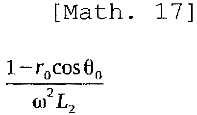
a resistance value of the adjustment resistor is expressed by
- The antenna circuit according to claim 1 further comprising:a capacitor connected in series with the second antenna; anda resistor connected in series with the second antenna.
- The antenna circuit according to claim 3, wherein
the adjustment capacitor is connected in parallel with a circuit including the second antenna, the capacitor, and the resistor, and
the adjustment resistor is connected in parallel with the circuit including the second antenna, the capacitor, and the resistor. - The antenna circuit according to claim 3, wherein
desired amplitude ratio r0 and phase difference θ0 are obtained under conditions where a capacitance value of the adjustment capacitor is expressed by
a resistance value of the adjustment resistor is expressed by
where r0 is an amplitude ratio between currents flowing through the first antenna and the second antenna, θ0 is a phase difference between the currents flowing through the first antenna and the second antenna, ω is an angular frequency of the currents flowing through the first antenna and the second antenna, L2 is the inductance of the second antenna, C2 is the capacitance value of the adjustment capacitor, and R2 is the resistance value of the adjustment resistor. - The antenna circuit according to claim 2 or 5, wherein
the amplitude ratio r0 is 1. - The antenna circuit according to claim 1, wherein
the first antenna and the second antenna are in a same shape.
Applications Claiming Priority (2)
| Application Number | Priority Date | Filing Date | Title |
|---|---|---|---|
| JP2017119519A JP6263662B1 (en) | 2017-06-19 | 2017-06-19 | Antenna circuit |
| PCT/JP2018/021558 WO2018235592A1 (en) | 2017-06-19 | 2018-06-05 | Antenna circuit |
Publications (3)
| Publication Number | Publication Date |
|---|---|
| EP3462541A1 true EP3462541A1 (en) | 2019-04-03 |
| EP3462541A4 EP3462541A4 (en) | 2020-01-15 |
| EP3462541B1 EP3462541B1 (en) | 2020-07-15 |
Family
ID=60989316
Family Applications (1)
| Application Number | Title | Priority Date | Filing Date |
|---|---|---|---|
| EP18800462.6A Active EP3462541B1 (en) | 2017-06-19 | 2018-06-05 | Antenna circuit |
Country Status (5)
| Country | Link |
|---|---|
| US (1) | US10498037B1 (en) |
| EP (1) | EP3462541B1 (en) |
| JP (1) | JP6263662B1 (en) |
| CN (1) | CN109429536B (en) |
| WO (1) | WO2018235592A1 (en) |
Family Cites Families (16)
| Publication number | Priority date | Publication date | Assignee | Title |
|---|---|---|---|---|
| JPS6059833B2 (en) | 1980-06-11 | 1985-12-26 | 東芝ライテック株式会社 | transistor inverter device |
| NL9201270A (en) * | 1992-07-15 | 1994-02-01 | Nedap Nv | ANTI-SHOP THEFT ANTENNA WITH ROTATING FIELD. |
| JP3337865B2 (en) * | 1995-04-22 | 2002-10-28 | ソニーケミカル株式会社 | Synthetic loop antenna |
| NL1011673C2 (en) * | 1999-03-25 | 2000-09-27 | Nedap Nv | Rotating field receiver for magnetic identification system. |
| US6960984B1 (en) * | 1999-12-08 | 2005-11-01 | University Of North Carolina | Methods and systems for reactively compensating magnetic current loops |
| JP2007104425A (en) * | 2005-10-05 | 2007-04-19 | General Res Of Electronics Inc | Receiver input circuit |
| JP2009071413A (en) | 2007-09-11 | 2009-04-02 | Hitachi Ltd | Antenna and RFID |
| US8487821B2 (en) * | 2009-06-08 | 2013-07-16 | Symbol Technologies, Inc. | Methods and apparatus for a low reflectivity compensated antenna |
| US9071289B2 (en) * | 2012-04-23 | 2015-06-30 | Cambridge Silicon Radio Limited | Transceiver supporting multiple modulation schemes |
| CN104167600A (en) * | 2013-05-16 | 2014-11-26 | 昆达电脑科技(昆山)有限公司 | Composite loop antenna |
| DE102013111027A1 (en) * | 2013-10-04 | 2015-04-09 | Infineon Technologies Ag | Multi-frequency antenna for miniaturized applications |
| KR20160068068A (en) * | 2014-12-04 | 2016-06-15 | 삼성전자주식회사 | Terminal device cover and radio frequency commuication device including radio frequency authentication module |
| JP6077036B2 (en) * | 2015-03-18 | 2017-02-08 | 日本電信電話株式会社 | Loop antenna |
| JP6069548B1 (en) * | 2016-01-22 | 2017-02-01 | 日本電信電話株式会社 | Loop antenna array group |
| JP6059833B1 (en) | 2016-01-26 | 2017-01-11 | 日本電信電話株式会社 | Magnetic field transmitter and magnetic field receiver |
| JP6059837B1 (en) * | 2016-03-22 | 2017-01-11 | 日本電信電話株式会社 | ANTENNA CONTROL DEVICE, ANTENNA CONTROL PROGRAM, AND ANTENNA CONTROL SYSTEM |
-
2017
- 2017-06-19 JP JP2017119519A patent/JP6263662B1/en active Active
-
2018
- 2018-06-05 EP EP18800462.6A patent/EP3462541B1/en active Active
- 2018-06-05 WO PCT/JP2018/021558 patent/WO2018235592A1/en not_active Ceased
- 2018-06-05 US US16/301,897 patent/US10498037B1/en active Active
- 2018-06-05 CN CN201880002019.6A patent/CN109429536B/en active Active
Also Published As
| Publication number | Publication date |
|---|---|
| US20190363441A1 (en) | 2019-11-28 |
| JP2019004411A (en) | 2019-01-10 |
| EP3462541A4 (en) | 2020-01-15 |
| JP6263662B1 (en) | 2018-01-17 |
| CN109429536B (en) | 2020-07-31 |
| WO2018235592A1 (en) | 2018-12-27 |
| CN109429536A (en) | 2019-03-05 |
| US10498037B1 (en) | 2019-12-03 |
| EP3462541B1 (en) | 2020-07-15 |
Similar Documents
| Publication | Publication Date | Title |
|---|---|---|
| EP4010714B1 (en) | Magnetic field-based current sensor for frequency-compensated measurement of alternating currents | |
| DE112019003906T5 (en) | Position sensing apparatus and method | |
| EP1987592A1 (en) | Inductive proximity switch and method for operating such a switch | |
| EP3462541B1 (en) | Antenna circuit | |
| EP3346553A1 (en) | Loop antenna array | |
| DE102006059137B3 (en) | Array antenna for magnetic resonance applications | |
| DE102019124391B4 (en) | Magnetic field-based current sensor for frequency-compensated measurement of alternating currents | |
| DE2722544C2 (en) | Measuring device for the inductive transformation of changes in position of an object | |
| DE3441174A1 (en) | GRADIENT FIELD COILS FOR IMAGING WITH NUCLEAR MAGNETIC RESONANCE | |
| DE102020206800A1 (en) | Phase shifter concept and radar transmitter concept | |
| EP1996900B1 (en) | Sensor for measuring distance using the phase shift of the magnetic field in an rc delay chain | |
| DE112018008038T5 (en) | Position sensing device and method | |
| US2231079A (en) | Phasing network | |
| DE2721993B2 (en) | Circuit arrangement for the transmission of digital direct current signals by means of carrier oscillations of a given frequency | |
| DE102017214180B4 (en) | Continuously digitally adjustable phase actuator | |
| DE2720240C3 (en) | Circuit arrangement for reducing the frequency instability of an oscillator | |
| DE202018005094U1 (en) | Balancing element with integrated impedance conversion and bandpass filter | |
| DE102012111839B4 (en) | Radar-based level measuring device with a synthesizer circuit | |
| DE102018222287A1 (en) | Inductive sensor | |
| DE2433196C3 (en) | Standard loop type magnetic field generator | |
| WO2006097071A1 (en) | Active reception antenna system | |
| US1751961A (en) | Alternating-current system | |
| DE102023003256A1 (en) | Intermodulation interference suppression circuit and method | |
| EP3097381B1 (en) | System and method for detecting the relative positions of two parts | |
| EP4600076A1 (en) | Method and system for inductive transmission of electrical energy, and method for producing an inductive energy transmission system |
Legal Events
| Date | Code | Title | Description |
|---|---|---|---|
| STAA | Information on the status of an ep patent application or granted ep patent |
Free format text: STATUS: UNKNOWN |
|
| STAA | Information on the status of an ep patent application or granted ep patent |
Free format text: STATUS: THE INTERNATIONAL PUBLICATION HAS BEEN MADE |
|
| PUAI | Public reference made under article 153(3) epc to a published international application that has entered the european phase |
Free format text: ORIGINAL CODE: 0009012 |
|
| STAA | Information on the status of an ep patent application or granted ep patent |
Free format text: STATUS: REQUEST FOR EXAMINATION WAS MADE |
|
| 17P | Request for examination filed |
Effective date: 20181122 |
|
| AK | Designated contracting states |
Kind code of ref document: A1 Designated state(s): AL AT BE BG CH CY CZ DE DK EE ES FI FR GB GR HR HU IE IS IT LI LT LU LV MC MK MT NL NO PL PT RO RS SE SI SK SM TR |
|
| AX | Request for extension of the european patent |
Extension state: BA ME |
|
| A4 | Supplementary search report drawn up and despatched |
Effective date: 20191213 |
|
| RIC1 | Information provided on ipc code assigned before grant |
Ipc: H01Q 7/00 20060101AFI20191209BHEP Ipc: H01Q 21/08 20060101ALI20191209BHEP Ipc: H04B 5/00 20060101ALI20191209BHEP Ipc: H01Q 5/335 20150101ALI20191209BHEP |
|
| GRAP | Despatch of communication of intention to grant a patent |
Free format text: ORIGINAL CODE: EPIDOSNIGR1 |
|
| STAA | Information on the status of an ep patent application or granted ep patent |
Free format text: STATUS: GRANT OF PATENT IS INTENDED |
|
| DAV | Request for validation of the european patent (deleted) | ||
| DAX | Request for extension of the european patent (deleted) | ||
| INTG | Intention to grant announced |
Effective date: 20200305 |
|
| GRAS | Grant fee paid |
Free format text: ORIGINAL CODE: EPIDOSNIGR3 |
|
| GRAA | (expected) grant |
Free format text: ORIGINAL CODE: 0009210 |
|
| STAA | Information on the status of an ep patent application or granted ep patent |
Free format text: STATUS: THE PATENT HAS BEEN GRANTED |
|
| AK | Designated contracting states |
Kind code of ref document: B1 Designated state(s): AL AT BE BG CH CY CZ DE DK EE ES FI FR GB GR HR HU IE IS IT LI LT LU LV MC MK MT NL NO PL PT RO RS SE SI SK SM TR |
|
| REG | Reference to a national code |
Ref country code: CH Ref legal event code: EP Ref country code: GB Ref legal event code: FG4D |
|
| REG | Reference to a national code |
Ref country code: IE Ref legal event code: FG4D |
|
| REG | Reference to a national code |
Ref country code: DE Ref legal event code: R096 Ref document number: 602018006123 Country of ref document: DE |
|
| REG | Reference to a national code |
Ref country code: AT Ref legal event code: REF Ref document number: 1292016 Country of ref document: AT Kind code of ref document: T Effective date: 20200815 |
|
| REG | Reference to a national code |
Ref country code: LT Ref legal event code: MG4D |
|
| REG | Reference to a national code |
Ref country code: AT Ref legal event code: MK05 Ref document number: 1292016 Country of ref document: AT Kind code of ref document: T Effective date: 20200715 |
|
| REG | Reference to a national code |
Ref country code: NL Ref legal event code: MP Effective date: 20200715 |
|
| PG25 | Lapsed in a contracting state [announced via postgrant information from national office to epo] |
Ref country code: LT Free format text: LAPSE BECAUSE OF FAILURE TO SUBMIT A TRANSLATION OF THE DESCRIPTION OR TO PAY THE FEE WITHIN THE PRESCRIBED TIME-LIMIT Effective date: 20200715 Ref country code: ES Free format text: LAPSE BECAUSE OF FAILURE TO SUBMIT A TRANSLATION OF THE DESCRIPTION OR TO PAY THE FEE WITHIN THE PRESCRIBED TIME-LIMIT Effective date: 20200715 Ref country code: PT Free format text: LAPSE BECAUSE OF FAILURE TO SUBMIT A TRANSLATION OF THE DESCRIPTION OR TO PAY THE FEE WITHIN THE PRESCRIBED TIME-LIMIT Effective date: 20201116 Ref country code: BG Free format text: LAPSE BECAUSE OF FAILURE TO SUBMIT A TRANSLATION OF THE DESCRIPTION OR TO PAY THE FEE WITHIN THE PRESCRIBED TIME-LIMIT Effective date: 20201015 Ref country code: SE Free format text: LAPSE BECAUSE OF FAILURE TO SUBMIT A TRANSLATION OF THE DESCRIPTION OR TO PAY THE FEE WITHIN THE PRESCRIBED TIME-LIMIT Effective date: 20200715 Ref country code: AT Free format text: LAPSE BECAUSE OF FAILURE TO SUBMIT A TRANSLATION OF THE DESCRIPTION OR TO PAY THE FEE WITHIN THE PRESCRIBED TIME-LIMIT Effective date: 20200715 Ref country code: GR Free format text: LAPSE BECAUSE OF FAILURE TO SUBMIT A TRANSLATION OF THE DESCRIPTION OR TO PAY THE FEE WITHIN THE PRESCRIBED TIME-LIMIT Effective date: 20201016 Ref country code: HR Free format text: LAPSE BECAUSE OF FAILURE TO SUBMIT A TRANSLATION OF THE DESCRIPTION OR TO PAY THE FEE WITHIN THE PRESCRIBED TIME-LIMIT Effective date: 20200715 Ref country code: NO Free format text: LAPSE BECAUSE OF FAILURE TO SUBMIT A TRANSLATION OF THE DESCRIPTION OR TO PAY THE FEE WITHIN THE PRESCRIBED TIME-LIMIT Effective date: 20201015 Ref country code: FI Free format text: LAPSE BECAUSE OF FAILURE TO SUBMIT A TRANSLATION OF THE DESCRIPTION OR TO PAY THE FEE WITHIN THE PRESCRIBED TIME-LIMIT Effective date: 20200715 |
|
| PG25 | Lapsed in a contracting state [announced via postgrant information from national office to epo] |
Ref country code: RS Free format text: LAPSE BECAUSE OF FAILURE TO SUBMIT A TRANSLATION OF THE DESCRIPTION OR TO PAY THE FEE WITHIN THE PRESCRIBED TIME-LIMIT Effective date: 20200715 Ref country code: LV Free format text: LAPSE BECAUSE OF FAILURE TO SUBMIT A TRANSLATION OF THE DESCRIPTION OR TO PAY THE FEE WITHIN THE PRESCRIBED TIME-LIMIT Effective date: 20200715 Ref country code: PL Free format text: LAPSE BECAUSE OF FAILURE TO SUBMIT A TRANSLATION OF THE DESCRIPTION OR TO PAY THE FEE WITHIN THE PRESCRIBED TIME-LIMIT Effective date: 20200715 Ref country code: IS Free format text: LAPSE BECAUSE OF FAILURE TO SUBMIT A TRANSLATION OF THE DESCRIPTION OR TO PAY THE FEE WITHIN THE PRESCRIBED TIME-LIMIT Effective date: 20201115 |
|
| PG25 | Lapsed in a contracting state [announced via postgrant information from national office to epo] |
Ref country code: NL Free format text: LAPSE BECAUSE OF FAILURE TO SUBMIT A TRANSLATION OF THE DESCRIPTION OR TO PAY THE FEE WITHIN THE PRESCRIBED TIME-LIMIT Effective date: 20200715 |
|
| REG | Reference to a national code |
Ref country code: DE Ref legal event code: R097 Ref document number: 602018006123 Country of ref document: DE |
|
| PG25 | Lapsed in a contracting state [announced via postgrant information from national office to epo] |
Ref country code: SM Free format text: LAPSE BECAUSE OF FAILURE TO SUBMIT A TRANSLATION OF THE DESCRIPTION OR TO PAY THE FEE WITHIN THE PRESCRIBED TIME-LIMIT Effective date: 20200715 Ref country code: IT Free format text: LAPSE BECAUSE OF FAILURE TO SUBMIT A TRANSLATION OF THE DESCRIPTION OR TO PAY THE FEE WITHIN THE PRESCRIBED TIME-LIMIT Effective date: 20200715 Ref country code: DK Free format text: LAPSE BECAUSE OF FAILURE TO SUBMIT A TRANSLATION OF THE DESCRIPTION OR TO PAY THE FEE WITHIN THE PRESCRIBED TIME-LIMIT Effective date: 20200715 Ref country code: CZ Free format text: LAPSE BECAUSE OF FAILURE TO SUBMIT A TRANSLATION OF THE DESCRIPTION OR TO PAY THE FEE WITHIN THE PRESCRIBED TIME-LIMIT Effective date: 20200715 Ref country code: RO Free format text: LAPSE BECAUSE OF FAILURE TO SUBMIT A TRANSLATION OF THE DESCRIPTION OR TO PAY THE FEE WITHIN THE PRESCRIBED TIME-LIMIT Effective date: 20200715 Ref country code: EE Free format text: LAPSE BECAUSE OF FAILURE TO SUBMIT A TRANSLATION OF THE DESCRIPTION OR TO PAY THE FEE WITHIN THE PRESCRIBED TIME-LIMIT Effective date: 20200715 |
|
| PLBE | No opposition filed within time limit |
Free format text: ORIGINAL CODE: 0009261 |
|
| STAA | Information on the status of an ep patent application or granted ep patent |
Free format text: STATUS: NO OPPOSITION FILED WITHIN TIME LIMIT |
|
| PG25 | Lapsed in a contracting state [announced via postgrant information from national office to epo] |
Ref country code: AL Free format text: LAPSE BECAUSE OF FAILURE TO SUBMIT A TRANSLATION OF THE DESCRIPTION OR TO PAY THE FEE WITHIN THE PRESCRIBED TIME-LIMIT Effective date: 20200715 |
|
| 26N | No opposition filed |
Effective date: 20210416 |
|
| PG25 | Lapsed in a contracting state [announced via postgrant information from national office to epo] |
Ref country code: SK Free format text: LAPSE BECAUSE OF FAILURE TO SUBMIT A TRANSLATION OF THE DESCRIPTION OR TO PAY THE FEE WITHIN THE PRESCRIBED TIME-LIMIT Effective date: 20200715 |
|
| PG25 | Lapsed in a contracting state [announced via postgrant information from national office to epo] |
Ref country code: SI Free format text: LAPSE BECAUSE OF FAILURE TO SUBMIT A TRANSLATION OF THE DESCRIPTION OR TO PAY THE FEE WITHIN THE PRESCRIBED TIME-LIMIT Effective date: 20200715 |
|
| PG25 | Lapsed in a contracting state [announced via postgrant information from national office to epo] |
Ref country code: MC Free format text: LAPSE BECAUSE OF FAILURE TO SUBMIT A TRANSLATION OF THE DESCRIPTION OR TO PAY THE FEE WITHIN THE PRESCRIBED TIME-LIMIT Effective date: 20200715 |
|
| REG | Reference to a national code |
Ref country code: CH Ref legal event code: PL |
|
| REG | Reference to a national code |
Ref country code: BE Ref legal event code: MM Effective date: 20210630 |
|
| PG25 | Lapsed in a contracting state [announced via postgrant information from national office to epo] |
Ref country code: LU Free format text: LAPSE BECAUSE OF NON-PAYMENT OF DUE FEES Effective date: 20210605 |
|
| PG25 | Lapsed in a contracting state [announced via postgrant information from national office to epo] |
Ref country code: LI Free format text: LAPSE BECAUSE OF NON-PAYMENT OF DUE FEES Effective date: 20210630 Ref country code: IE Free format text: LAPSE BECAUSE OF NON-PAYMENT OF DUE FEES Effective date: 20210605 Ref country code: CH Free format text: LAPSE BECAUSE OF NON-PAYMENT OF DUE FEES Effective date: 20210630 |
|
| PG25 | Lapsed in a contracting state [announced via postgrant information from national office to epo] |
Ref country code: BE Free format text: LAPSE BECAUSE OF NON-PAYMENT OF DUE FEES Effective date: 20210630 |
|
| PG25 | Lapsed in a contracting state [announced via postgrant information from national office to epo] |
Ref country code: CY Free format text: LAPSE BECAUSE OF FAILURE TO SUBMIT A TRANSLATION OF THE DESCRIPTION OR TO PAY THE FEE WITHIN THE PRESCRIBED TIME-LIMIT Effective date: 20200715 |
|
| PG25 | Lapsed in a contracting state [announced via postgrant information from national office to epo] |
Ref country code: HU Free format text: LAPSE BECAUSE OF FAILURE TO SUBMIT A TRANSLATION OF THE DESCRIPTION OR TO PAY THE FEE WITHIN THE PRESCRIBED TIME-LIMIT; INVALID AB INITIO Effective date: 20180605 |
|
| PG25 | Lapsed in a contracting state [announced via postgrant information from national office to epo] |
Ref country code: MK Free format text: LAPSE BECAUSE OF FAILURE TO SUBMIT A TRANSLATION OF THE DESCRIPTION OR TO PAY THE FEE WITHIN THE PRESCRIBED TIME-LIMIT Effective date: 20200715 |
|
| PG25 | Lapsed in a contracting state [announced via postgrant information from national office to epo] |
Ref country code: MT Free format text: LAPSE BECAUSE OF FAILURE TO SUBMIT A TRANSLATION OF THE DESCRIPTION OR TO PAY THE FEE WITHIN THE PRESCRIBED TIME-LIMIT Effective date: 20200715 |
|
| PGFP | Annual fee paid to national office [announced via postgrant information from national office to epo] |
Ref country code: DE Payment date: 20250618 Year of fee payment: 8 |
|
| PGFP | Annual fee paid to national office [announced via postgrant information from national office to epo] |
Ref country code: GB Payment date: 20250618 Year of fee payment: 8 |
|
| PGFP | Annual fee paid to national office [announced via postgrant information from national office to epo] |
Ref country code: FR Payment date: 20250625 Year of fee payment: 8 |
|
| PG25 | Lapsed in a contracting state [announced via postgrant information from national office to epo] |
Ref country code: TR Free format text: LAPSE BECAUSE OF FAILURE TO SUBMIT A TRANSLATION OF THE DESCRIPTION OR TO PAY THE FEE WITHIN THE PRESCRIBED TIME-LIMIT Effective date: 20200715 |
|
| REG | Reference to a national code |
Ref country code: DE Ref legal event code: R081 Ref document number: 602018006123 Country of ref document: DE Owner name: NTT, INC., JP Free format text: FORMER OWNER: NIPPON TELEGRAPH AND TELEPHONE CORPORATION, TOKYO, JP Ref country code: DE Ref legal event code: R082 Ref document number: 602018006123 Country of ref document: DE Representative=s name: DENNEMEYER & ASSOCIATES RECHTSANWALTSGESELLSCH, DE |