EP3462508A2 - High-voltage capacitor, system including the capacitor, and method for manufacturing the capacitor - Google Patents
High-voltage capacitor, system including the capacitor, and method for manufacturing the capacitor Download PDFInfo
- Publication number
- EP3462508A2 EP3462508A2 EP18197797.6A EP18197797A EP3462508A2 EP 3462508 A2 EP3462508 A2 EP 3462508A2 EP 18197797 A EP18197797 A EP 18197797A EP 3462508 A2 EP3462508 A2 EP 3462508A2
- Authority
- EP
- European Patent Office
- Prior art keywords
- layer
- forming
- dielectric
- dielectric layer
- capacitor
- Prior art date
- Legal status (The legal status is an assumption and is not a legal conclusion. Google has not performed a legal analysis and makes no representation as to the accuracy of the status listed.)
- Granted
Links
Images




Classifications
-
- H—ELECTRICITY
- H10—SEMICONDUCTOR DEVICES; ELECTRIC SOLID-STATE DEVICES NOT OTHERWISE PROVIDED FOR
- H10D—INORGANIC ELECTRIC SEMICONDUCTOR DEVICES
- H10D1/00—Resistors, capacitors or inductors
- H10D1/60—Capacitors
- H10D1/68—Capacitors having no potential barriers
- H10D1/692—Electrodes
-
- H—ELECTRICITY
- H10—SEMICONDUCTOR DEVICES; ELECTRIC SOLID-STATE DEVICES NOT OTHERWISE PROVIDED FOR
- H10D—INORGANIC ELECTRIC SEMICONDUCTOR DEVICES
- H10D1/00—Resistors, capacitors or inductors
- H10D1/60—Capacitors
- H10D1/68—Capacitors having no potential barriers
-
- H—ELECTRICITY
- H01—ELECTRIC ELEMENTS
- H01G—CAPACITORS; CAPACITORS, RECTIFIERS, DETECTORS, SWITCHING DEVICES, LIGHT-SENSITIVE OR TEMPERATURE-SENSITIVE DEVICES OF THE ELECTROLYTIC TYPE
- H01G2/00—Details of capacitors not covered by a single one of groups H01G4/00-H01G11/00
- H01G2/22—Electrostatic or magnetic shielding
-
- H—ELECTRICITY
- H01—ELECTRIC ELEMENTS
- H01G—CAPACITORS; CAPACITORS, RECTIFIERS, DETECTORS, SWITCHING DEVICES, LIGHT-SENSITIVE OR TEMPERATURE-SENSITIVE DEVICES OF THE ELECTROLYTIC TYPE
- H01G4/00—Fixed capacitors; Processes of their manufacture
- H01G4/002—Details
- H01G4/018—Dielectrics
- H01G4/06—Solid dielectrics
- H01G4/14—Organic dielectrics
-
- H—ELECTRICITY
- H01—ELECTRIC ELEMENTS
- H01G—CAPACITORS; CAPACITORS, RECTIFIERS, DETECTORS, SWITCHING DEVICES, LIGHT-SENSITIVE OR TEMPERATURE-SENSITIVE DEVICES OF THE ELECTROLYTIC TYPE
- H01G4/00—Fixed capacitors; Processes of their manufacture
- H01G4/002—Details
- H01G4/228—Terminals
- H01G4/252—Terminals the terminals being coated on the capacitive element
-
- H—ELECTRICITY
- H01—ELECTRIC ELEMENTS
- H01G—CAPACITORS; CAPACITORS, RECTIFIERS, DETECTORS, SWITCHING DEVICES, LIGHT-SENSITIVE OR TEMPERATURE-SENSITIVE DEVICES OF THE ELECTROLYTIC TYPE
- H01G4/00—Fixed capacitors; Processes of their manufacture
- H01G4/30—Stacked capacitors
- H01G4/306—Stacked capacitors made by thin film techniques
-
- H—ELECTRICITY
- H01—ELECTRIC ELEMENTS
- H01G—CAPACITORS; CAPACITORS, RECTIFIERS, DETECTORS, SWITCHING DEVICES, LIGHT-SENSITIVE OR TEMPERATURE-SENSITIVE DEVICES OF THE ELECTROLYTIC TYPE
- H01G4/00—Fixed capacitors; Processes of their manufacture
- H01G4/33—Thin- or thick-film capacitors (thin- or thick-film circuits; capacitors without a potential-jump or surface barrier specially adapted for integrated circuits, details thereof, multistep manufacturing processes therefor)
Definitions
- the present invention relates to a high-voltage capacitor, to a system including the capacitor, and to a method for manufacturing the capacitor.
- High-voltage (HV) capacitors for integrated circuits are known, configured for enabling the transmission of signals at high frequencies, for example of the order of megahertz, between conductive elements biased at a very high difference of potential, for example around 10 kV or of the order of tens of kilovolts, and that hence require electrical insulation; see, for example, the document No. US 2016/0133690 .
- Said HV capacitors typically have dielectric layers of a thickness large enough to present a breakdown voltage higher than the difference of potential at which, in use, its terminals are biased.
- FIG. 1 shows, in a triaxial system of orthogonal coordinates x, y, z, a lateral cross-sectional view in the plane xz of a HV capacitor 1 of a known type.
- the HV capacitor 1 comprises a substrate 2, a bottom electrode 4, which extends over the substrate 2, a dielectric layer 6, which extends over the bottom electrode 4, and a top electrode 8, which extends over the dielectric layer 6.
- the portion of the dielectric layer 6 set on top, in plan view in the plane xy, of the top electrode 8 and the bottom electrode 4 constitutes the active area 9 of the HV capacitor 1, offering the highest contribution to the capacitance of the HV capacitor 1.
- a recess 10 extends throughout the thickness of the dielectric layer 6 so as to expose a contact region 12 of the bottom electrode 4, and hence enable electrical contact of the bottom electrode 4.
- the thickness of the dielectric layer 6 is such as to obtain the desired breakdown voltage and is typically in the region of a few tens of micrometres.
- a further mechanism of breakdown of HV capacitors is due to the accumulation over time of contaminating particles on the top surface of the dielectric layer 6, which may form a surface conductive path between the top electrode 8 and the contact region 12, drastically reducing the lateral surface resistance between the top electrode 8 and the contact region 12 and introducing excessive leakage currents.
- the presence of humidity on the top surface of the dielectric layer 6 may reduce the surface resistance and favour conductive phenomena. In these conditions, arc short circuits may be set up between edges of the top surface of the dielectric layer 6 (facing the contact region 12) and the contact region 12.
- the aim of the present invention is to provide a capacitor, a system including the capacitor, and a method for manufacturing the capacitor, designed to overcome the drawbacks of the known art.
- a capacitor According to the present invention a capacitor, a system including the capacitor, and a method for manufacturing the capacitor are provided, as defined in the annexed claims.
- Figure 2 shows, in a triaxial system of orthogonal coordinates x, y, z, a lateral cross-sectional view in the plane xz of a capacitor 21.
- the capacitor 21 is of a type for use in high voltage or extra-high voltage applications (referred to hereinafter also generically as HV).
- HV high voltage or extra-high voltage
- the HV capacitor 21 comprises a substrate 22, which extends between a front surface 22a thereof (parallel to the plane xy) and a rear surface 22b thereof (parallel to the plane xy).
- the substrate 22 is made of insulating material, such as silicon dioxide (SiO 2 ), having a thickness, for example, ranging between 0.5 ⁇ m and 2 ⁇ m, in particular 0.7 ⁇ m (which can be deposited on a substrate, for example, made of high-resistivity silicon).
- Figure 3 shows a HV capacitor 31 according to a further embodiment.
- the HV capacitor 31 differs from the HV capacitor 21 exclusively as regards the material of the substrate 22.
- the substrate 22 of the HV capacitor 31 comprises a high-resistivity substrate 24 and a field plate oxide layer 26, which extends over the high-resistivity substrate 24.
- the high-resistivity substrate is, for example, made of polysilicon or silicon with high electrical resistivity, for example higher than 1000 ⁇ cm, and has a thickness ranging between 100 ⁇ m and 500 ⁇ m, in particular 280 ⁇ m.
- the field plate oxide layer 26 is, for example, made of silicon dioxide and has a thickness ranging between 0.5 ⁇ m and 2 ⁇ m, in particular 0.7 ⁇ m.
- the HV capacitor 21 of Figure 2 further comprises a bottom electrode 28, which extends over the substrate 22.
- the bottom electrode 28 is made of conductive material, such as aluminium or copper and has a thickness, for example, ranging between 0.5 ⁇ m and 3 ⁇ m, in particular 1.5 ⁇ m.
- a protective layer 30 extends over the bottom electrode 28, in order to protect the bottom electrode 28 preventing oxidation thereof.
- the protective layer 30 is made of titanium or titanium nitride (TiN) and has a thickness, for example, ranging between 20 nm and 50 nm, in particular 30 nm. In other embodiments, the protective layer 30 could be omitted.
- the HV capacitor 21 further comprises a dielectric multilayer 32, which extends over the protective layer 30.
- the dielectric multilayer 32 extends over the bottom electrode 28.
- the dielectric multilayer 32 comprises a first dielectric layer 34, for example made of tetraethyl orthosilicate (TEOS) or of silicon dioxide that can be obtained by any process of deposition on metal material.
- the first dielectric layer has a thickness, for example, ranging between 1 ⁇ m and 2 ⁇ m, in particular 1 ⁇ m.
- the dielectric multilayer 32 comprises a second dielectric layer 36, which extends over the first dielectric layer 34.
- the second dielectric layer 36 is made of a material different from that of the first dielectric layer 34, for example silicon nitride (Si 3 N x ) or silicon oxynitride (SiO x N y ) and has a thickness, for example, ranging between 1 ⁇ m and 2 ⁇ m, in particular 1 ⁇ m.
- a number of depositions and a number of dielectric materials to form the dielectric multilayer 32 minimises the possibility of having structural defects that extend throughout the thickness of the dielectric multilayer 32.
- the second dielectric layer 36 may be omitted.
- the dielectric multilayer 32 further comprises a third dielectric layer 38, which extends over the second dielectric layer 36.
- the third dielectric layer 38 extends over the first dielectric layer 34.
- the third dielectric layer 38 is made of polymeric material that can be laid in a conformable way, such as polyimide (PI), and has a thickness ranging between 10 ⁇ m and 30 ⁇ m, in particular 20 ⁇ m.
- the dielectric multilayer 32 comprises a recess 40, which extends throughout its thickness, exposing a contact region 42 of the protective layer 30 and hence enabling electrical contact of the bottom electrode 28 of the HV capacitor 21, for example via wire bonding techniques.
- the contact region 42 extends directly over the bottom electrode 28.
- the HV capacitor 21 further comprises a top electrode 46, which extends over the dielectric multilayer 32.
- the top electrode 46 is made of conductive material, such as gold, and has a thickness ranging between 0.1 ⁇ m and 0.2 ⁇ m, in particular 0.1 ⁇ m. Use of gold is preferable to facilitate wire bonding techniques.
- the HV capacitor 21 further comprises a barrier layer 44, which extends between the top electrode 46 and the dielectric multilayer 32, in order to hinder the migration of atoms of the top electrode 46 towards the dielectric multilayer 32 that could favour undesired conductive paths between the top electrode 46 and the bottom electrode 28.
- the barrier layer 44 is made of metal material, such as titanium, and has a thickness, for example, ranging between 30 nm and 100 nm, in particular 50 nm.
- the area of extension of the top electrode 46 delimits an overlap region between the top electrode 46, the dielectric multilayer 32, and the bottom electrode 28, referred to in what follows as "active area 48".
- the HV capacitor 21 is a parallel-plate capacitor having an area limited by the area of extension of the top electrode 46.
- the area of extension of the top electrode 46, in plan view in the plane xy ranges between 80 ⁇ 80 ⁇ m 2 and 200 ⁇ 200 ⁇ m 2 , in particular 100 ⁇ 100 ⁇ m 2 , and has a shape chosen from rectangular, circular, elliptical, polygonal, or polygonal with rounded corners.
- the first dielectric layer 34 has a plurality of openings 50 in a region set between the active area 48 and the contact region 42. In the embodiments in which the second dielectric layer 36 is present, also this has a plurality of openings 50 aligned along the axis z to the plurality of openings 50 of the first dielectric layer 34.
- the portion of the dielectric multilayer 32 included in the active area 48 has a constant thickness t ox , given by the sum of the thicknesses of the dielectric layers that make it up, whereas the portion of the dielectric multilayer 32 external to the active area 48 has a thickness ranging between a maximum value, corresponding to t ox , and a minimum value t min , corresponding to the thickness of just the third dielectric layer 38.
- the third dielectric layer 38 has depressions or grooves 37 at the openings 50.
- the third dielectric layer 38 has a top surface 38a that, in lateral cross-sectional view in the plane xz, has an undulated profile.
- the length of the surface resistive path between the top electrode 46 and the contact region 42 increases as compared to the embodiment of a known type illustrated in Figure 1 , wherein the dielectric layer does not have any grooves 37. Consequently, given the same surface resistance between the top electrode 46 and the contact region 42, the HV capacitors 21, 31 of the respective embodiments of Figures 2 and 3 are more compact than the HV capacitor 1 of a known type of Figure 1 .
- the openings 50 have a main direction of extension orthogonal to the direction of propagation of the current between the top electrode 46 and the contact region 42.
- the main direction of extension of the openings 50 is not orthogonal to the direction of propagation of the current, and forms an angle ranging between 20° and 90° with the direction of propagation of the current between the top electrode 46 and the contact region 42.
- the main direction of extension of the openings 50 not to be parallel to the direction of propagation of the current between the top electrode 46 and the contact region 42.
- FIG 4 is a lateral cross-sectional view in the plane xz of a HV capacitor 41 according to a further embodiment of the present invention.
- the HV capacitor 41 differs from the HV capacitor 31 of Figure 3 due to the presence of further layers forming the substrate 22.
- Elements of the HV capacitor 41 that are common to the HV capacitor 31 are designated by the same reference numbers and are not described any further herein.
- the substrate 22 of the HV capacitor 41 further comprises an electromagnetic shield layer 51, which extends over the field plate oxide layer 26 in order to protect the HV capacitor 41 from electromagnetic disturbances coming from outside.
- the electromagnetic shield layer 51 is made of conductive material, such as doped polysilicon or metal, and has a thickness, for example, ranging between 0.3 ⁇ m and 1.5 ⁇ m, in particular 0.5 ⁇ m.
- the substrate 22 of the HV capacitor 41 further comprises an insulating layer 52, which extends over the electromagnetic shield layer 51.
- the insulating layer 52 is, for example, made of tetraethyl orthosilicate (TEOS) or of silicon dioxide that can be obtained by any process of deposition on metal material and has a thickness, for example, ranging between 0.5 ⁇ m and 0.7 ⁇ m, in particular 0.5 ⁇ m.
- TEOS tetraethyl orthosilicate
- the insulating layer 52 functions as electrical insulating layer between the electromagnetic shield layer 51 and the bottom electrode 28.
- the electromagnetic shield layer 51 is electrically connected to an electrical terminal 58 through an opening of the insulating layer 52, enabling, in use, biasing of the electromagnetic shield layer 51 at a reference voltage.
- the electrical terminal 58 is formed starting from the same deposition of metal material as that of the bottom electrode 28 and creating an opening designed to insulate the bottom electrode 28 electrically from the electrical terminal 58.
- the protective layer 30 also extends over the electrical terminal 58, in order to protect the electrical terminal 58 from oxidation phenomena.
- the high-resistivity substrate 24 and the field plate oxide layer 26 are replaced by a substrate made of insulating material, such as silicon dioxide (SiO 2 ), having a thickness, for example, ranging between 200 ⁇ m and 600 ⁇ m, in particular 300 ⁇ m.
- the electromagnetic shield layer 51 extends directly over the substrate made of insulating material.
- Described with reference to Figures 5A-5F are steps of a method for manufacturing the HV transistor 41 of Figure 4 .
- a wafer which includes the high-resistivity substrate 24. This is followed by the step of forming the field plate oxide layer 26 on the high-resistivity substrate 24, for example via thermal growth of silicon dioxide. There then follows the step of forming the electromagnetic shield layer 51 on the field plate oxide layer 26, for example via deposition of doped polysilicon or a metal layer.
- the step of forming the insulating layer 52 is carried out, for example via deposition of a TEOS layer and masked etching of the TEOS layer to form an opening 70, which extends throughout the thickness of the TEOS layer, in a region corresponding to the electromagnetic shield layer 51, where, in subsequent steps of the manufacturing method, an electrical contact with the electrical terminal 58 will be formed.
- the substrate 22 is thus formed.
- a first conductive layer 72 is carried out, for example via deposition of metal material, such as aluminium or copper on the insulating layer 52, simultaneously filling the opening 70 and hence forming an electrical contact between the electromagnetic layer 51 and the first conductive layer 72.
- a second conductive layer 74 is formed on the first conductive layer 72, for example via deposition of metal material, such as titanium or titanium nitride (TiN).
- an opening 76 which is laterally staggered with respect to the opening 70 and extends throughout the thickness of the first and second conductive layers 72, 74 in order to insulate electrically from one another two regions of the first conductive layer 72, which form the bottom electrode 28 and the electrical terminal 58, respectively.
- the opening 76 entirely surrounds the electrical terminal 58.
- the second conductive layer 74 thus forms the protective layer 30.
- the opening 76 is formed, for example, via dry chemical etching.
- the step of forming the first dielectric layer 34 is carried out, for example via deposition of TEOS or SiO 2 obtained via CVD or PECVD.
- the first dielectric layer 34 fills the opening 76 entirely and extends over the protective layer 30.
- the step of forming the second dielectric layer 36 on the first dielectric layer 34 made of a material different from that of the first dielectric layer 34, for example silicon nitride (Si 3 N x ) or silicon oxynitride (SiO x N y ).
- the step of masked etching of the first and second dielectric layers 34, 36 comprises forming an opening 84 in a position corresponding to the electrical terminal 58, partially exposing the region of the protective layer 30 on the electrical terminal 58.
- an opening 86 is formed in a region of the bottom electrode 28 where the contact region 42 will be formed, laterally staggered with respect to the opening 76 formed, in the step of Figure 5C , in the first conductive layer.
- Part of an electrical insulating structure 80 is thus formed between the bottom electrode 28 and the electrical terminal 58.
- a plurality of openings 50 is formed, laterally staggered with respect to the opening 86.
- the opening 86 extends between the plurality of openings 50 and the electrical insulating structure 80.
- the openings 50 have an extension L h , measured along the axis x, comprised, for example, between 20 ⁇ m and 30 ⁇ m, in particular 20 ⁇ m.
- the openings 50 are set at equal distances apart from one another.
- the number of openings 50 is, for example, between 2 and 20, for example 10.
- each opening of the plurality of openings 50 is separated from an adjacent opening by a spacer 88 formed by the first and second dielectric layers 78, 82 and having an extension L s , measured along the axis x, comprised, for example, between 5 ⁇ m and 20 ⁇ m, in particular 10 ⁇ m. Consequently, the extension D obtained from the sum of the extension L s of each spacer 88 and the extension L h of each opening 50 is between 55 ⁇ m and 1020 ⁇ m.
- the step of forming the third dielectric layer 38 is carried out, for example, via spin coating of polyimide or another polymer capable of following in a conformable way the topography due to the spacers 88, also for thicknesses of the third dielectric layer 38 of some tens of micrometers.
- the third dielectric layer 38 fills the openings 50, 84, 86 of the first and second dielectric layers 34, 36 completely.
- the step of forming a third conductive layer 90 on the third dielectric layer 38 is carried out, for example, via sputtering of metal material, such as titanium.
- a fourth conductive layer 92 on the third conductive layer 90 is then followed by the step of forming a fourth conductive layer 92 on the third conductive layer 90, for example via sputtering of metal material, such as gold.
- the step of masked etching of the third and fourth conductive layers 90, 92 is carried out, for example by wet or dry chemical etching, so as to remove the third and fourth conductive layers 90, 92 entirely, except for regions that, in plan view in the plane xy, delimit the active area 48 of the HV capacitor 41.
- the barrier layer 44 and the top electrode 46 are thus formed.
- Figure 6 shows a block diagram of an electronic system 100 comprising a HV capacitor 21 or 31 or 41, according to the respective embodiment described previously.
- the electronic system 100 comprises a first electronic circuit 101 and a second electronic circuit 105, coupled to one another via the HV capacitor 21, 31, 41.
- the first and second electronic circuits 101, 105 may be integrated on respective dies coupled to one another and housed in one and the same package.
- An input terminal 102 of the first electronic circuit 101 is configured for receiving an input signal S in1 .
- the input terminal 102 is electrically coupled to a processing circuit 103 of the first electronic circuit 101.
- the processing circuit 103 is configured for processing the input signal S in1 and generating a first output signal S out1 at high frequency, on an output terminal 104 of the first electronic circuit 101.
- the second electronic circuit 105 houses the HV capacitor 21, 31, 41.
- the output terminal 104 of the first electronic circuit 101 is electrically coupled to the contact region 42 of the HV capacitor 21, 31, 41, for example by means of wire bonding techniques.
- the HV capacitor 21, 31, 41 is likewise electrically coupled to a processing circuit 107 of the second electrical circuit 105, configured for acquiring an output signal from the HV capacitor 21, 31, 41, processing said signal, and generating a second output signal S out2 .
- Electrical coupling between the first and second electronic circuits 101, 105 by means of the HV capacitor 21, 31, 41 enables transfer between the processing circuit 103 and the processing circuit 107 of the information associated with the first output signal S out1 also in the case where there is a high difference of potential (for example, in the region of 10 kV) between the d.c. component of the first output signal S out1 and the voltage accepted at input by the processing circuit 107 of the second electrical circuit 105.
- an electromagnetic shield layer 51 in the substrate 22 enables reduction of the sensitivity of the HV capacitor 21 to electromagnetic disturbances coming from other components of the circuit in which it is integrated or coming from outside.
Landscapes
- Engineering & Computer Science (AREA)
- Power Engineering (AREA)
- Microelectronics & Electronic Packaging (AREA)
- Manufacturing & Machinery (AREA)
- Semiconductor Integrated Circuits (AREA)
- Ceramic Capacitors (AREA)
- Fixed Capacitors And Capacitor Manufacturing Machines (AREA)
Abstract
Description
- This application claims priority from Italian Patent Application No.
102017000108913 filed on 28/09/2017 - The present invention relates to a high-voltage capacitor, to a system including the capacitor, and to a method for manufacturing the capacitor.
- High-voltage (HV) capacitors for integrated circuits are known, configured for enabling the transmission of signals at high frequencies, for example of the order of megahertz, between conductive elements biased at a very high difference of potential, for example around 10 kV or of the order of tens of kilovolts, and that hence require electrical insulation; see, for example, the document No.
US 2016/0133690 . - Said HV capacitors typically have dielectric layers of a thickness large enough to present a breakdown voltage higher than the difference of potential at which, in use, its terminals are biased.
-
Figure 1 shows, in a triaxial system of orthogonal coordinates x, y, z, a lateral cross-sectional view in the plane xz of a HV capacitor 1 of a known type. The HV capacitor 1 comprises asubstrate 2, abottom electrode 4, which extends over thesubstrate 2, adielectric layer 6, which extends over thebottom electrode 4, and atop electrode 8, which extends over thedielectric layer 6. The portion of thedielectric layer 6 set on top, in plan view in the plane xy, of thetop electrode 8 and thebottom electrode 4 constitutes theactive area 9 of the HV capacitor 1, offering the highest contribution to the capacitance of the HV capacitor 1. - A
recess 10 extends throughout the thickness of thedielectric layer 6 so as to expose acontact region 12 of thebottom electrode 4, and hence enable electrical contact of thebottom electrode 4. - The thickness of the
dielectric layer 6 is such as to obtain the desired breakdown voltage and is typically in the region of a few tens of micrometres. - The present applicant has found that a further mechanism of breakdown of HV capacitors is due to the accumulation over time of contaminating particles on the top surface of the
dielectric layer 6, which may form a surface conductive path between thetop electrode 8 and thecontact region 12, drastically reducing the lateral surface resistance between thetop electrode 8 and thecontact region 12 and introducing excessive leakage currents. Moreover, also the presence of humidity on the top surface of thedielectric layer 6 may reduce the surface resistance and favour conductive phenomena. In these conditions, arc short circuits may be set up between edges of the top surface of the dielectric layer 6 (facing the contact region 12) and thecontact region 12. - The aim of the present invention is to provide a capacitor, a system including the capacitor, and a method for manufacturing the capacitor, designed to overcome the drawbacks of the known art.
- According to the present invention a capacitor, a system including the capacitor, and a method for manufacturing the capacitor are provided, as defined in the annexed claims.
- For a better understanding of the present invention preferred embodiments will now be described, purely by way of non-limiting example, with reference to the attached drawings, wherein:
-
Figure 1 is a schematic cross-sectional view of a high-voltage (HV) capacitor according to an embodiment of a known type; -
Figure 2 is a schematic cross-sectional view of a HV capacitor according to an embodiment of the present invention; -
Figure 3 is a schematic cross-sectional view of a HV capacitor according to another embodiment of the present invention; -
Figure 4 is a schematic cross-sectional view of a HV capacitor according to a further embodiment of the present invention; -
Figures 5A-5F show a method for manufacturing the HV capacitor ofFigure 4 ; and -
Figure 6 shows a block diagram of an electronic system including a HV capacitor according to any one of the embodiments of the present invention. -
Figure 2 shows, in a triaxial system of orthogonal coordinates x, y, z, a lateral cross-sectional view in the plane xz of acapacitor 21. In particular, thecapacitor 21 is of a type for use in high voltage or extra-high voltage applications (referred to hereinafter also generically as HV). In this context, by "high voltage" or "extra-high voltage" are meant voltages ranging between 5 000 V and 20 000 V. - The
HV capacitor 21 comprises asubstrate 22, which extends between afront surface 22a thereof (parallel to the plane xy) and arear surface 22b thereof (parallel to the plane xy). In the embodiment ofFigure 2 , thesubstrate 22 is made of insulating material, such as silicon dioxide (SiO2), having a thickness, for example, ranging between 0.5 µm and 2 µm, in particular 0.7 µm (which can be deposited on a substrate, for example, made of high-resistivity silicon).Figure 3 shows aHV capacitor 31 according to a further embodiment. TheHV capacitor 31 differs from theHV capacitor 21 exclusively as regards the material of thesubstrate 22. Thesubstrate 22 of theHV capacitor 31 comprises a high-resistivity substrate 24 and a fieldplate oxide layer 26, which extends over the high-resistivity substrate 24. The high-resistivity substrate is, for example, made of polysilicon or silicon with high electrical resistivity, for example higher than 1000 Ω·cm, and has a thickness ranging between 100 µm and 500 µm, in particular 280 µm. The fieldplate oxide layer 26 is, for example, made of silicon dioxide and has a thickness ranging between 0.5 µm and 2 µm, in particular 0.7 µm. - The
HV capacitor 21 ofFigure 2 further comprises abottom electrode 28, which extends over thesubstrate 22. Thebottom electrode 28 is made of conductive material, such as aluminium or copper and has a thickness, for example, ranging between 0.5 µm and 3 µm, in particular 1.5 µm. Preferably, aprotective layer 30 extends over thebottom electrode 28, in order to protect thebottom electrode 28 preventing oxidation thereof. For instance, theprotective layer 30 is made of titanium or titanium nitride (TiN) and has a thickness, for example, ranging between 20 nm and 50 nm, in particular 30 nm. In other embodiments, theprotective layer 30 could be omitted. - The
HV capacitor 21 further comprises adielectric multilayer 32, which extends over theprotective layer 30. In embodiments in which theprotective layer 30 is not present, thedielectric multilayer 32 extends over thebottom electrode 28. - The
dielectric multilayer 32 comprises a firstdielectric layer 34, for example made of tetraethyl orthosilicate (TEOS) or of silicon dioxide that can be obtained by any process of deposition on metal material. The first dielectric layer has a thickness, for example, ranging between 1 µm and 2 µm, in particular 1 µm. - Preferably, the
dielectric multilayer 32 comprises a seconddielectric layer 36, which extends over the firstdielectric layer 34. The seconddielectric layer 36 is made of a material different from that of the firstdielectric layer 34, for example silicon nitride (Si3Nx) or silicon oxynitride (SiOxNy) and has a thickness, for example, ranging between 1 µm and 2 µm, in particular 1 µm. Use of a number of depositions and a number of dielectric materials to form thedielectric multilayer 32 minimises the possibility of having structural defects that extend throughout the thickness of thedielectric multilayer 32. The seconddielectric layer 36 may be omitted. - The
dielectric multilayer 32 further comprises a thirddielectric layer 38, which extends over the seconddielectric layer 36. In embodiments in which the seconddielectric layer 36 is not present, the thirddielectric layer 38 extends over the firstdielectric layer 34. According to an aspect of the present invention, the thirddielectric layer 38 is made of polymeric material that can be laid in a conformable way, such as polyimide (PI), and has a thickness ranging between 10 µm and 30 µm, in particular 20 µm. - The
dielectric multilayer 32 comprises arecess 40, which extends throughout its thickness, exposing acontact region 42 of theprotective layer 30 and hence enabling electrical contact of thebottom electrode 28 of theHV capacitor 21, for example via wire bonding techniques. In embodiments in which theprotective layer 30 is omitted, thecontact region 42 extends directly over thebottom electrode 28. - The
HV capacitor 21 further comprises atop electrode 46, which extends over thedielectric multilayer 32. Thetop electrode 46 is made of conductive material, such as gold, and has a thickness ranging between 0.1 µm and 0.2 µm, in particular 0.1 µm. Use of gold is preferable to facilitate wire bonding techniques. Preferably, theHV capacitor 21 further comprises abarrier layer 44, which extends between thetop electrode 46 and thedielectric multilayer 32, in order to hinder the migration of atoms of thetop electrode 46 towards thedielectric multilayer 32 that could favour undesired conductive paths between thetop electrode 46 and thebottom electrode 28. Thebarrier layer 44 is made of metal material, such as titanium, and has a thickness, for example, ranging between 30 nm and 100 nm, in particular 50 nm. - The area of extension of the
top electrode 46, in plan view in the plane xy, delimits an overlap region between thetop electrode 46, thedielectric multilayer 32, and thebottom electrode 28, referred to in what follows as "active area 48". In other words, theHV capacitor 21 is a parallel-plate capacitor having an area limited by the area of extension of thetop electrode 46. The area of extension of thetop electrode 46, in plan view in the plane xy, ranges between 80 × 80 µm2 and 200 × 200 µm2, in particular 100 × 100 µm2, and has a shape chosen from rectangular, circular, elliptical, polygonal, or polygonal with rounded corners. - The
first dielectric layer 34 has a plurality ofopenings 50 in a region set between theactive area 48 and thecontact region 42. In the embodiments in which thesecond dielectric layer 36 is present, also this has a plurality ofopenings 50 aligned along the axis z to the plurality ofopenings 50 of thefirst dielectric layer 34. Consequently, the portion of thedielectric multilayer 32 included in theactive area 48 has a constant thickness t ox, given by the sum of the thicknesses of the dielectric layers that make it up, whereas the portion of thedielectric multilayer 32 external to theactive area 48 has a thickness ranging between a maximum value, corresponding to t ox, and a minimum value t min, corresponding to the thickness of just thethird dielectric layer 38. In other words, thethird dielectric layer 38 has depressions orgrooves 37 at theopenings 50. In particular, thethird dielectric layer 38 has atop surface 38a that, in lateral cross-sectional view in the plane xz, has an undulated profile. Consequently, the length of the surface resistive path between thetop electrode 46 and thecontact region 42 increases as compared to the embodiment of a known type illustrated inFigure 1 , wherein the dielectric layer does not have anygrooves 37. Consequently, given the same surface resistance between thetop electrode 46 and thecontact region 42, theHV capacitors Figures 2 and3 are more compact than the HV capacitor 1 of a known type ofFigure 1 . - According to one embodiment, the
openings 50 have a main direction of extension orthogonal to the direction of propagation of the current between thetop electrode 46 and thecontact region 42. - According to another embodiment, the main direction of extension of the
openings 50 is not orthogonal to the direction of propagation of the current, and forms an angle ranging between 20° and 90° with the direction of propagation of the current between thetop electrode 46 and thecontact region 42. - In general, it is in any case expedient for the main direction of extension of the
openings 50 not to be parallel to the direction of propagation of the current between thetop electrode 46 and thecontact region 42. -
Figure 4 is a lateral cross-sectional view in the plane xz of aHV capacitor 41 according to a further embodiment of the present invention. TheHV capacitor 41 differs from theHV capacitor 31 ofFigure 3 due to the presence of further layers forming thesubstrate 22. Elements of theHV capacitor 41 that are common to theHV capacitor 31 are designated by the same reference numbers and are not described any further herein. - In particular, the
substrate 22 of theHV capacitor 41 further comprises anelectromagnetic shield layer 51, which extends over the fieldplate oxide layer 26 in order to protect theHV capacitor 41 from electromagnetic disturbances coming from outside. Theelectromagnetic shield layer 51 is made of conductive material, such as doped polysilicon or metal, and has a thickness, for example, ranging between 0.3 µm and 1.5 µm, in particular 0.5 µm. - The
substrate 22 of theHV capacitor 41 further comprises an insulatinglayer 52, which extends over theelectromagnetic shield layer 51. The insulatinglayer 52 is, for example, made of tetraethyl orthosilicate (TEOS) or of silicon dioxide that can be obtained by any process of deposition on metal material and has a thickness, for example, ranging between 0.5 µm and 0.7 µm, in particular 0.5 µm. - The insulating
layer 52 functions as electrical insulating layer between theelectromagnetic shield layer 51 and thebottom electrode 28. Theelectromagnetic shield layer 51 is electrically connected to anelectrical terminal 58 through an opening of the insulatinglayer 52, enabling, in use, biasing of theelectromagnetic shield layer 51 at a reference voltage. According to an aspect of the present invention, theelectrical terminal 58 is formed starting from the same deposition of metal material as that of thebottom electrode 28 and creating an opening designed to insulate thebottom electrode 28 electrically from theelectrical terminal 58. Preferably, theprotective layer 30 also extends over theelectrical terminal 58, in order to protect the electrical terminal 58 from oxidation phenomena. - In another embodiment (not illustrated), the high-
resistivity substrate 24 and the fieldplate oxide layer 26 are replaced by a substrate made of insulating material, such as silicon dioxide (SiO2), having a thickness, for example, ranging between 200 µm and 600 µm, in particular 300 µm. In this case, theelectromagnetic shield layer 51 extends directly over the substrate made of insulating material. - Described with reference to
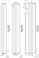
Figures 5A-5F are steps of a method for manufacturing theHV transistor 41 ofFigure 4 . - With reference to
Figure 5A , a wafer is provided, which includes the high-resistivity substrate 24. This is followed by the step of forming the fieldplate oxide layer 26 on the high-resistivity substrate 24, for example via thermal growth of silicon dioxide. There then follows the step of forming theelectromagnetic shield layer 51 on the fieldplate oxide layer 26, for example via deposition of doped polysilicon or a metal layer. - Then (
Figure 5B ), the step of forming the insulatinglayer 52 is carried out, for example via deposition of a TEOS layer and masked etching of the TEOS layer to form anopening 70, which extends throughout the thickness of the TEOS layer, in a region corresponding to theelectromagnetic shield layer 51, where, in subsequent steps of the manufacturing method, an electrical contact with theelectrical terminal 58 will be formed. Thesubstrate 22 is thus formed. - Then (
Figure 5C ), the step of forming a first conductive layer 72 is carried out, for example via deposition of metal material, such as aluminium or copper on the insulatinglayer 52, simultaneously filling theopening 70 and hence forming an electrical contact between theelectromagnetic layer 51 and the first conductive layer 72. Then, a secondconductive layer 74 is formed on the first conductive layer 72, for example via deposition of metal material, such as titanium or titanium nitride (TiN). - This is followed by the step of forming an
opening 76, which is laterally staggered with respect to theopening 70 and extends throughout the thickness of the first and secondconductive layers 72, 74 in order to insulate electrically from one another two regions of the first conductive layer 72, which form thebottom electrode 28 and theelectrical terminal 58, respectively. For instance, in plan view in the plane xy, theopening 76 entirely surrounds theelectrical terminal 58. The secondconductive layer 74 thus forms theprotective layer 30. Theopening 76 is formed, for example, via dry chemical etching. - Then (
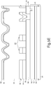
Figure 5D ), the step of forming thefirst dielectric layer 34 is carried out, for example via deposition of TEOS or SiO2 obtained via CVD or PECVD. Thefirst dielectric layer 34 fills theopening 76 entirely and extends over theprotective layer 30. This is followed by the step of forming thesecond dielectric layer 36 on thefirst dielectric layer 34, made of a material different from that of thefirst dielectric layer 34, for example silicon nitride (Si3Nx) or silicon oxynitride (SiOxNy). - There then follows the step of masked etching of the first and second dielectric layers 34, 36 in order to form a plurality of openings, which extend throughout the thickness of the first and second dielectric layers 34, 36, exposing respective regions of the
protective layer 30. - The step of masked etching of the first and second dielectric layers 34, 36 comprises forming an
opening 84 in a position corresponding to theelectrical terminal 58, partially exposing the region of theprotective layer 30 on theelectrical terminal 58. Simultaneously, anopening 86 is formed in a region of thebottom electrode 28 where thecontact region 42 will be formed, laterally staggered with respect to theopening 76 formed, in the step ofFigure 5C , in the first conductive layer. Part of an electricalinsulating structure 80 is thus formed between thebottom electrode 28 and theelectrical terminal 58. Simultaneously, a plurality ofopenings 50 is formed, laterally staggered with respect to theopening 86. In other words, theopening 86 extends between the plurality ofopenings 50 and the electrical insulatingstructure 80. Theopenings 50 have an extension L h, measured along the axis x, comprised, for example, between 20 µm and 30 µm, in particular 20 µm. In a non-limiting embodiment, theopenings 50 are set at equal distances apart from one another. The number ofopenings 50 is, for example, between 2 and 20, for example 10. Consequently, each opening of the plurality ofopenings 50 is separated from an adjacent opening by aspacer 88 formed by the first and second dielectric layers 78, 82 and having an extension L s, measured along the axis x, comprised, for example, between 5 µm and 20 µm, in particular 10 µm. Consequently, the extension D obtained from the sum of the extension L s of eachspacer 88 and the extension L h of eachopening 50 is between 55 µm and 1020 µm. - Next (
Figure 5E ), the step of forming thethird dielectric layer 38 is carried out, for example, via spin coating of polyimide or another polymer capable of following in a conformable way the topography due to thespacers 88, also for thicknesses of thethird dielectric layer 38 of some tens of micrometers. Thethird dielectric layer 38 fills theopenings - Then, the step of forming a third
conductive layer 90 on thethird dielectric layer 38 is carried out, for example, via sputtering of metal material, such as titanium. - This is then followed by the step of forming a fourth
conductive layer 92 on the thirdconductive layer 90, for example via sputtering of metal material, such as gold. - Next (
Figure 5F ), the step of masked etching of the third and fourthconductive layers conductive layers active area 48 of theHV capacitor 41. Thebarrier layer 44 and thetop electrode 46 are thus formed. - There then follows the step of masked etching of the
third dielectric layer 38, to form the recess 40 (and expose the contact region 42) and another recess in a position corresponding to theelectrical terminal 58, partially exposing the region of theprotective layer 30 on theelectrical terminal 58. TheHV capacitor 41 ofFigure 4 is thus obtained. -
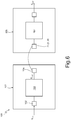
Figure 6 shows a block diagram of anelectronic system 100 comprising aHV capacitor electronic system 100 comprises a firstelectronic circuit 101 and a secondelectronic circuit 105, coupled to one another via theHV capacitor electronic circuits - An
input terminal 102 of the firstelectronic circuit 101 is configured for receiving an input signal S in1. Theinput terminal 102 is electrically coupled to aprocessing circuit 103 of the firstelectronic circuit 101. Theprocessing circuit 103 is configured for processing the input signal S in1 and generating a first output signal S out1 at high frequency, on anoutput terminal 104 of the firstelectronic circuit 101. The secondelectronic circuit 105 houses theHV capacitor output terminal 104 of the firstelectronic circuit 101 is electrically coupled to thecontact region 42 of theHV capacitor HV capacitor processing circuit 107 of the secondelectrical circuit 105, configured for acquiring an output signal from theHV capacitor electronic circuits HV capacitor processing circuit 103 and theprocessing circuit 107 of the information associated with the first output signal S out1 also in the case where there is a high difference of potential (for example, in the region of 10 kV) between the d.c. component of the first output signal S out1 and the voltage accepted at input by theprocessing circuit 107 of the secondelectrical circuit 105. - From an examination of the characteristics of the invention described and illustrated herein, the advantages that it affords are evident.
- For instance, obtaining a curvilinear surface profile of the
third dielectric layer 38, by formation ofspacers 88, enables an increase in the length, and hence resistance, of the lateral surface path between thetop electrode 46 and thecontact region 42 of thebottom electrode 28. Consequently, given the same surface resistance between thetop electrode 46 and thecontact region 42, theHV capacitors Figures 2 ,3 ,4 are more compact than the HV capacitor 1 according to the embodiment of a known type represented inFigure 1 . - Moreover, the integration of an
electromagnetic shield layer 51 in thesubstrate 22 enables reduction of the sensitivity of theHV capacitor 21 to electromagnetic disturbances coming from other components of the circuit in which it is integrated or coming from outside. - Finally, it is clear that modifications and variations may be made to the disclosure described and illustrated herein, without thereby departing from the sphere of protection of the present invention, as defined in the annexed claims.
Claims (25)
- A capacitor (21; 31; 41), comprising:a substrate (22);a bottom plate, which extends over the substrate and includes a first conductive layer (28);a top plate, which extends over the bottom plate and includes a second conductive layer (46);a contact region (42), electrically coupled to the first conductive layer (28); anda first dielectric layer (38), which extends between the bottom plate and the top plate,characterized in that the first dielectric layer (38) defines a surface path (38a) between the second conductive layer (46) and the contact region (42) andhas a plurality of grooves (37) which increase the length of said surface path.
- The capacitor according to Claim 1, wherein said surface path includes a plurality of surface resistive electrical paths between the second conductive layer (46) and the contact region (42), and wherein the shortest resistive electrical path of said plurality of resistive electrical paths ranges between 60 µm and 1060 µm.
- The capacitor according to Claim 1, wherein said surface path between the second conductive layer (46) and the contact region (42) includes a plurality of resistive electrical paths, which connect the second conductive layer (46) and the contact region (42), said grooves having a respective main direction of surface extension that forms an angle with the shortest resistive electrical path of said plurality of resistive electrical paths.
- The capacitor according to Claim 3, wherein said angle is about 90°.
- The capacitor according to any one of the preceding claims, wherein the first dielectric layer (38) includes a first dielectric region (48), which extends between the bottom plate and the top plate, and a second dielectric region which extends between the first dielectric region and the contact region (42), the second dielectric region being contiguous to the first dielectric region (48), said grooves (37) being formed in correspondence to said second dielectric region.
- The capacitor according to claim 5, further comprising a thickness-enhancement body (34, 36), of dielectric material, which extends over the second dielectric layer (34), said thickness-enhancement body (34, 36) extending continuously in the first dielectric region (48) between the bottom plate and the first dielectric layer (38) and having discontinuities (50) in the second dielectric region,
wherein the first dielectric layer (38) is of a polymeric material configured for reproducing, at the surface level, said discontinuities (50) in a conformable way, to form said grooves (37). - The capacitor according to Claim 6, wherein said thickness-enhancement body (34, 36) is a multilayer comprising a second dielectric layer (34) including tetraethyl orthosilicate or silicon oxide and a third dielectric layer (36), including silicon nitride or silicon oxynitride, which extends over the second dielectric layer (34) .
- The capacitor according to any one of the preceding claims, wherein said first dielectric layer (38) is of polyimide.
- The capacitor according to any one of the preceding claims, wherein said first dielectric layer (38) reaches a maximum height (tox), measured starting from said bottom plate and in a direction orthogonal to a plane of lie of the bottom plate, ranging between 12 µm and 32 µm and a minimum height (tmin), measured in said direction starting from said bottom plate, ranging between 8 µm and 28 µm,
wherein the first dielectric region has a uniform thickness in said orthogonal direction up to said maximum height,
and wherein said minimum height is reached in the second dielectric region in respective points of maximum depth of each groove (37). - The capacitor according to any one of the preceding claims, wherein said bottom plate further includes a protective layer (30), of conductive material, which extends over, and in contact with, the first conductive layer (28),
said protective layer (30) being of a material not subject to oxidation when exposed to a working environment. - The capacitor according to any one of the preceding claims, wherein said top plate further includes a barrier layer (44), of conductive material, which extends between the second conductive layer (46) and the first dielectric layer (38),
said barrier layer (44) being of a material designed to inhibit a migration of conductive species from the second conductive layer (46) to the first dielectric layer (38). - The capacitor according to any one of the preceding claims, further comprising:an electromagnetic shield layer (51), of conductive material, between the substrate and the bottom plate, designed to shield electromagnetic disturbances coming from an environment external to said capacitor (41); andan electrical-decoupling layer (52), of insulating material, which extends between the electromagnetic shield layer (51) and the bottom plate.
- The capacitor according to Claim 12, further comprising a pad in electrical contact with the electromagnetic shield layer (51) designed to bias, in use, the electromagnetic shield layer (51) at a biasing voltage.
- An electronic system (100) comprising:a first electronic circuit (103) configured for generating an output signal (S out1) having a first voltage and a frequency value;a second electronic circuit (107), coupled to the first electronic circuit (103), configured for accepting at input a signal having a second voltage value lower than the first voltage value; anda capacitor (21; 31; 41) according to any one of claims 1-13, coupled between the first electronic circuit (103) and the second electronic circuit (107), designed to transfer information associated with the frequency of the output signal (S out1).
- A method for manufacturing a capacitor (21; 31; 41), comprising the steps of:forming, on a substrate (22), a bottom plate, which includes a first conductive layer (28);forming, on the substrate (22), a contact region (42) electrically coupled to the first conductive layer (28);forming a first dielectric layer (38), on the bottom plate; andforming a top plate, of conductive material (46), on the first dielectric layer (38),the first dielectric layer (38) forming a surface path (38a) between the second conductive layer (46) and the contact region (42),characterized in that the step of forming the first dielectric layer (38) includes forming the first dielectric layer (38) in such a way to define a plurality of surface grooves (37) which increase the spatial extension of said surface path.
- The method according to Claim 15, wherein said surface path between the second conductive layer (46) and the contact region (42) includes a plurality of resistive electrical paths that connect the second conductive layer (46) and the contact region (42),
the step of forming the grooves including forming said grooves with a main surface direction of extension that forms an angle with the shortest resistive electrical path of said plurality of resistive paths. - The method according to either Claim 15 or Claim 16, wherein the step of forming the first dielectric layer (38) includes the substeps of forming a first dielectric region (48) on the bottom plate and forming a second dielectric region, which is contiguous to the first dielectric region (48) and extends as far as the contact region (42), thus defining the surface path (38a) between the second conductive layer (46) and the contact region (42),
the step of forming the plurality of forming the plurality of grooves (37) comprising forming the plurality of forming the plurality of grooves (37) in the second dielectric region. - The method according to Claim 17, further comprising the steps of (i) forming a thickness-enhancement body (34, 36), of dielectric material, on the bottom plate; (ii) removing selective portions of the thickness-enhancement body (34, 36) in such a way that said thickness-enhancement body (34, 36) extends continuously in the first dielectric region (48) and discontinuously in the second dielectric region,
and wherein the step of forming the first dielectric layer (38) includes depositing or spinning, in a conformable way on the thickness-enhancement body (34, 36), a polymeric material, thus simultaneously forming said grooves. - The method according to Claim 18, wherein the step of removing selective portions of the thickness-enhancement body (34, 36) in a discontinuous way comprises carrying out a masked etch of the thickness-enhancement body (34, 36) throughout its thickness to form a plurality of trenches.
- The method according to Claim 18 or Claim 19, wherein the step of forming said thickness-enhancement body (34, 36) comprises the step of forming a multilayer, including the substeps of: forming a second dielectric layer (34) of tetraethyl orthosilicate or silicon oxide, and forming a third dielectric layer (36), of silicon nitride or silicon oxynitride, on the second dielectric layer (34).
- The method according to any one of Claims 15-20, wherein the step of forming said first dielectric layer (38) includes depositing or spinning polyimide.
- The method according to any one of Claims 15-21, wherein the step of forming the bottom plate further includes forming a protective layer (30), of conductive material, on, and in contact with, the first conductive layer (28), said protective layer (30) being of a material not subject to oxidation when exposed to a working environment.
- The method according to any one of Claims 15-22, wherein the step of forming the top plate further includes forming a barrier layer (44), of conductive material, between the second conductive layer (46) and the first dielectric layer (38), said barrier layer (44) being of a material that is able to inhibit migration of conductive species from the second conductive layer (46) to the first dielectric layer (38) .
- The method according to any one of Claims 15-23, further comprising the step of:forming an electromagnetic shield layer (51), of conductive material between the substrate and the bottom plate, which is designed to shield electromagnetic disturbances coming from an environment external to said capacitor (41); andforming an electrical-decoupling layer (52), of insulating material, between the electromagnetic shield layer (51) and the bottom plate.
- The method according to Claims 24, wherein the step of forming the electromagnetic shield layer (51) includes depositing conductive material.
Applications Claiming Priority (1)
| Application Number | Priority Date | Filing Date | Title |
|---|---|---|---|
| IT102017000108913A IT201700108913A1 (en) | 2017-09-28 | 2017-09-28 | CONDENSER FOR HIGH VOLTAGES, SYSTEM INCLUDING THE CONDENSER AND METHOD OF MANUFACTURING THE CONDENSER |
Publications (3)
| Publication Number | Publication Date |
|---|---|
| EP3462508A2 true EP3462508A2 (en) | 2019-04-03 |
| EP3462508A3 EP3462508A3 (en) | 2019-05-29 |
| EP3462508B1 EP3462508B1 (en) | 2020-08-12 |
Family
ID=61006268
Family Applications (1)
| Application Number | Title | Priority Date | Filing Date |
|---|---|---|---|
| EP18197797.6A Active EP3462508B1 (en) | 2017-09-28 | 2018-09-28 | High-voltage capacitor, system including the capacitor, and method for manufacturing the capacitor |
Country Status (3)
| Country | Link |
|---|---|
| EP (1) | EP3462508B1 (en) |
| CN (2) | CN109585426B (en) |
| IT (1) | IT201700108913A1 (en) |
Families Citing this family (1)
| Publication number | Priority date | Publication date | Assignee | Title |
|---|---|---|---|---|
| IT201700108913A1 (en) * | 2017-09-28 | 2019-03-28 | St Microelectronics Srl | CONDENSER FOR HIGH VOLTAGES, SYSTEM INCLUDING THE CONDENSER AND METHOD OF MANUFACTURING THE CONDENSER |
Citations (1)
| Publication number | Priority date | Publication date | Assignee | Title |
|---|---|---|---|---|
| US20160133690A1 (en) | 2014-11-06 | 2016-05-12 | Texas Instruments Incorporated | Methods and Apparatus for High Voltage Integrated Circuit Capacitors |
Family Cites Families (6)
| Publication number | Priority date | Publication date | Assignee | Title |
|---|---|---|---|---|
| JPH03104273A (en) * | 1989-09-19 | 1991-05-01 | Mitsubishi Electric Corp | Semiconductor memory and manufacture thereof |
| KR100640065B1 (en) * | 2005-03-02 | 2006-10-31 | 삼성전자주식회사 | MIM capacitor including ground shield layer |
| JP2007142109A (en) * | 2005-11-17 | 2007-06-07 | Tdk Corp | Electronic components |
| KR102093458B1 (en) * | 2013-07-05 | 2020-03-26 | 삼성디스플레이 주식회사 | Capacitor |
| CN204991474U (en) * | 2015-10-19 | 2016-01-20 | 昆山萬豐電子有限公司 | Ann's rule piece formula ceramic capacitor |
| IT201700108913A1 (en) * | 2017-09-28 | 2019-03-28 | St Microelectronics Srl | CONDENSER FOR HIGH VOLTAGES, SYSTEM INCLUDING THE CONDENSER AND METHOD OF MANUFACTURING THE CONDENSER |
-
2017
- 2017-09-28 IT IT102017000108913A patent/IT201700108913A1/en unknown
-
2018
- 2018-09-27 CN CN201811134253.2A patent/CN109585426B/en active Active
- 2018-09-27 CN CN201821582633.8U patent/CN209087832U/en active Active
- 2018-09-28 EP EP18197797.6A patent/EP3462508B1/en active Active
Patent Citations (1)
| Publication number | Priority date | Publication date | Assignee | Title |
|---|---|---|---|---|
| US20160133690A1 (en) | 2014-11-06 | 2016-05-12 | Texas Instruments Incorporated | Methods and Apparatus for High Voltage Integrated Circuit Capacitors |
Also Published As
| Publication number | Publication date |
|---|---|
| EP3462508B1 (en) | 2020-08-12 |
| CN109585426A (en) | 2019-04-05 |
| CN109585426B (en) | 2023-04-11 |
| EP3462508A3 (en) | 2019-05-29 |
| IT201700108913A1 (en) | 2019-03-28 |
| CN209087832U (en) | 2019-07-09 |
Similar Documents
| Publication | Publication Date | Title |
|---|---|---|
| KR100815172B1 (en) | Capacitor | |
| US6498381B2 (en) | Semiconductor structures having multiple conductive layers in an opening, and methods for fabricating same | |
| US8748308B2 (en) | Through wafer vias and method of making same | |
| US7323785B2 (en) | Semiconductor device | |
| JP5048230B2 (en) | Semiconductor device and manufacturing method thereof | |
| JP5209301B2 (en) | Technology and RF circuit design to reduce substrate crosstalk for mixed signals | |
| JP2021509540A (en) | High voltage insulation structure and method | |
| US20050156221A1 (en) | Semiconductor device and method of manufacturing same | |
| CN113054104A (en) | Top cap structure for isolated capacitor | |
| US6924725B2 (en) | Coil on a semiconductor substrate and method for its production | |
| JP2012009481A (en) | Semiconductor device and method of manufacturing the same | |
| US12543562B2 (en) | Capacitive isolator and method for manufacturing thereof | |
| US7479424B2 (en) | Method for fabricating an integrated circuit comprising a three-dimensional capacitor | |
| EP3462508B1 (en) | High-voltage capacitor, system including the capacitor, and method for manufacturing the capacitor | |
| US7678659B2 (en) | Method of reducing current leakage in a metal insulator metal semiconductor capacitor and semiconductor capacitor thereof | |
| US11189559B2 (en) | Semiconductor device and fabrication method thereof | |
| US11574996B2 (en) | High-voltage capacitor, system including the capacitor and method for manufacturing the capacitor | |
| TW502425B (en) | Semiconductor-device and its production method | |
| KR20100071206A (en) | Mim capacitor of semiconductor device and manufacturing method thereof | |
| CN119480849B (en) | Semiconductor devices and their manufacturing methods | |
| US20260122926A1 (en) | Serpentine high voltage resistor over silicon substrate | |
| CN115394753B (en) | Far infrared sensing element, manufacturing method and sensing dielectric layer thickness determining method | |
| JP2003045989A (en) | Semiconductor device and semiconductor manufacturing method | |
| HK40055473A (en) | Top hat structure for isolation capacitors | |
| CN121054605A (en) | Semiconductor devices and their fabrication methods, electronic devices |
Legal Events
| Date | Code | Title | Description |
|---|---|---|---|
| PUAI | Public reference made under article 153(3) epc to a published international application that has entered the european phase |
Free format text: ORIGINAL CODE: 0009012 |
|
| STAA | Information on the status of an ep patent application or granted ep patent |
Free format text: STATUS: THE APPLICATION HAS BEEN PUBLISHED |
|
| AK | Designated contracting states |
Kind code of ref document: A2 Designated state(s): AL AT BE BG CH CY CZ DE DK EE ES FI FR GB GR HR HU IE IS IT LI LT LU LV MC MK MT NL NO PL PT RO RS SE SI SK SM TR |
|
| AX | Request for extension of the european patent |
Extension state: BA ME |
|
| PUAL | Search report despatched |
Free format text: ORIGINAL CODE: 0009013 |
|
| AK | Designated contracting states |
Kind code of ref document: A3 Designated state(s): AL AT BE BG CH CY CZ DE DK EE ES FI FR GB GR HR HU IE IS IT LI LT LU LV MC MK MT NL NO PL PT RO RS SE SI SK SM TR |
|
| AX | Request for extension of the european patent |
Extension state: BA ME |
|
| RIC1 | Information provided on ipc code assigned before grant |
Ipc: H01G 4/252 20060101ALI20190424BHEP Ipc: H01G 2/22 20060101ALI20190424BHEP Ipc: H01G 4/30 20060101ALI20190424BHEP Ipc: H01L 49/02 20060101AFI20190424BHEP Ipc: H01G 4/14 20060101ALI20190424BHEP Ipc: H01G 4/33 20060101ALI20190424BHEP |
|
| STAA | Information on the status of an ep patent application or granted ep patent |
Free format text: STATUS: REQUEST FOR EXAMINATION WAS MADE |
|
| 17P | Request for examination filed |
Effective date: 20191126 |
|
| RBV | Designated contracting states (corrected) |
Designated state(s): AL AT BE BG CH CY CZ DE DK EE ES FI FR GB GR HR HU IE IS IT LI LT LU LV MC MK MT NL NO PL PT RO RS SE SI SK SM TR |
|
| GRAP | Despatch of communication of intention to grant a patent |
Free format text: ORIGINAL CODE: EPIDOSNIGR1 |
|
| STAA | Information on the status of an ep patent application or granted ep patent |
Free format text: STATUS: GRANT OF PATENT IS INTENDED |
|
| INTG | Intention to grant announced |
Effective date: 20200311 |
|
| GRAS | Grant fee paid |
Free format text: ORIGINAL CODE: EPIDOSNIGR3 |
|
| GRAA | (expected) grant |
Free format text: ORIGINAL CODE: 0009210 |
|
| STAA | Information on the status of an ep patent application or granted ep patent |
Free format text: STATUS: THE PATENT HAS BEEN GRANTED |
|
| AK | Designated contracting states |
Kind code of ref document: B1 Designated state(s): AL AT BE BG CH CY CZ DE DK EE ES FI FR GB GR HR HU IE IS IT LI LT LU LV MC MK MT NL NO PL PT RO RS SE SI SK SM TR |
|
| REG | Reference to a national code |
Ref country code: CH Ref legal event code: EP |
|
| REG | Reference to a national code |
Ref country code: IE Ref legal event code: FG4D |
|
| REG | Reference to a national code |
Ref country code: DE Ref legal event code: R096 Ref document number: 602018006853 Country of ref document: DE |
|
| REG | Reference to a national code |
Ref country code: AT Ref legal event code: REF Ref document number: 1302417 Country of ref document: AT Kind code of ref document: T Effective date: 20200915 |
|
| REG | Reference to a national code |
Ref country code: LT Ref legal event code: MG4D |
|
| REG | Reference to a national code |
Ref country code: NL Ref legal event code: MP Effective date: 20200812 |
|
| PG25 | Lapsed in a contracting state [announced via postgrant information from national office to epo] |
Ref country code: FI Free format text: LAPSE BECAUSE OF FAILURE TO SUBMIT A TRANSLATION OF THE DESCRIPTION OR TO PAY THE FEE WITHIN THE PRESCRIBED TIME-LIMIT Effective date: 20200812 Ref country code: NO Free format text: LAPSE BECAUSE OF FAILURE TO SUBMIT A TRANSLATION OF THE DESCRIPTION OR TO PAY THE FEE WITHIN THE PRESCRIBED TIME-LIMIT Effective date: 20201112 Ref country code: GR Free format text: LAPSE BECAUSE OF FAILURE TO SUBMIT A TRANSLATION OF THE DESCRIPTION OR TO PAY THE FEE WITHIN THE PRESCRIBED TIME-LIMIT Effective date: 20201113 Ref country code: LT Free format text: LAPSE BECAUSE OF FAILURE TO SUBMIT A TRANSLATION OF THE DESCRIPTION OR TO PAY THE FEE WITHIN THE PRESCRIBED TIME-LIMIT Effective date: 20200812 Ref country code: HR Free format text: LAPSE BECAUSE OF FAILURE TO SUBMIT A TRANSLATION OF THE DESCRIPTION OR TO PAY THE FEE WITHIN THE PRESCRIBED TIME-LIMIT Effective date: 20200812 Ref country code: SE Free format text: LAPSE BECAUSE OF FAILURE TO SUBMIT A TRANSLATION OF THE DESCRIPTION OR TO PAY THE FEE WITHIN THE PRESCRIBED TIME-LIMIT Effective date: 20200812 Ref country code: BG Free format text: LAPSE BECAUSE OF FAILURE TO SUBMIT A TRANSLATION OF THE DESCRIPTION OR TO PAY THE FEE WITHIN THE PRESCRIBED TIME-LIMIT Effective date: 20201112 |
|
| REG | Reference to a national code |
Ref country code: AT Ref legal event code: MK05 Ref document number: 1302417 Country of ref document: AT Kind code of ref document: T Effective date: 20200812 |
|
| PG25 | Lapsed in a contracting state [announced via postgrant information from national office to epo] |
Ref country code: PL Free format text: LAPSE BECAUSE OF FAILURE TO SUBMIT A TRANSLATION OF THE DESCRIPTION OR TO PAY THE FEE WITHIN THE PRESCRIBED TIME-LIMIT Effective date: 20200812 Ref country code: RS Free format text: LAPSE BECAUSE OF FAILURE TO SUBMIT A TRANSLATION OF THE DESCRIPTION OR TO PAY THE FEE WITHIN THE PRESCRIBED TIME-LIMIT Effective date: 20200812 Ref country code: LV Free format text: LAPSE BECAUSE OF FAILURE TO SUBMIT A TRANSLATION OF THE DESCRIPTION OR TO PAY THE FEE WITHIN THE PRESCRIBED TIME-LIMIT Effective date: 20200812 Ref country code: NL Free format text: LAPSE BECAUSE OF FAILURE TO SUBMIT A TRANSLATION OF THE DESCRIPTION OR TO PAY THE FEE WITHIN THE PRESCRIBED TIME-LIMIT Effective date: 20200812 Ref country code: IS Free format text: LAPSE BECAUSE OF FAILURE TO SUBMIT A TRANSLATION OF THE DESCRIPTION OR TO PAY THE FEE WITHIN THE PRESCRIBED TIME-LIMIT Effective date: 20201212 |
|
| PG25 | Lapsed in a contracting state [announced via postgrant information from national office to epo] |
Ref country code: SM Free format text: LAPSE BECAUSE OF FAILURE TO SUBMIT A TRANSLATION OF THE DESCRIPTION OR TO PAY THE FEE WITHIN THE PRESCRIBED TIME-LIMIT Effective date: 20200812 Ref country code: DK Free format text: LAPSE BECAUSE OF FAILURE TO SUBMIT A TRANSLATION OF THE DESCRIPTION OR TO PAY THE FEE WITHIN THE PRESCRIBED TIME-LIMIT Effective date: 20200812 Ref country code: CZ Free format text: LAPSE BECAUSE OF FAILURE TO SUBMIT A TRANSLATION OF THE DESCRIPTION OR TO PAY THE FEE WITHIN THE PRESCRIBED TIME-LIMIT Effective date: 20200812 Ref country code: RO Free format text: LAPSE BECAUSE OF FAILURE TO SUBMIT A TRANSLATION OF THE DESCRIPTION OR TO PAY THE FEE WITHIN THE PRESCRIBED TIME-LIMIT Effective date: 20200812 Ref country code: EE Free format text: LAPSE BECAUSE OF FAILURE TO SUBMIT A TRANSLATION OF THE DESCRIPTION OR TO PAY THE FEE WITHIN THE PRESCRIBED TIME-LIMIT Effective date: 20200812 |
|
| REG | Reference to a national code |
Ref country code: DE Ref legal event code: R097 Ref document number: 602018006853 Country of ref document: DE |
|
| PG25 | Lapsed in a contracting state [announced via postgrant information from national office to epo] |
Ref country code: MC Free format text: LAPSE BECAUSE OF FAILURE TO SUBMIT A TRANSLATION OF THE DESCRIPTION OR TO PAY THE FEE WITHIN THE PRESCRIBED TIME-LIMIT Effective date: 20200812 Ref country code: AT Free format text: LAPSE BECAUSE OF FAILURE TO SUBMIT A TRANSLATION OF THE DESCRIPTION OR TO PAY THE FEE WITHIN THE PRESCRIBED TIME-LIMIT Effective date: 20200812 Ref country code: AL Free format text: LAPSE BECAUSE OF FAILURE TO SUBMIT A TRANSLATION OF THE DESCRIPTION OR TO PAY THE FEE WITHIN THE PRESCRIBED TIME-LIMIT Effective date: 20200812 Ref country code: ES Free format text: LAPSE BECAUSE OF FAILURE TO SUBMIT A TRANSLATION OF THE DESCRIPTION OR TO PAY THE FEE WITHIN THE PRESCRIBED TIME-LIMIT Effective date: 20200812 |
|
| PLBE | No opposition filed within time limit |
Free format text: ORIGINAL CODE: 0009261 |
|
| REG | Reference to a national code |
Ref country code: BE Ref legal event code: MM Effective date: 20200930 |
|
| STAA | Information on the status of an ep patent application or granted ep patent |
Free format text: STATUS: NO OPPOSITION FILED WITHIN TIME LIMIT |
|
| PG25 | Lapsed in a contracting state [announced via postgrant information from national office to epo] |
Ref country code: LU Free format text: LAPSE BECAUSE OF NON-PAYMENT OF DUE FEES Effective date: 20200928 Ref country code: SK Free format text: LAPSE BECAUSE OF FAILURE TO SUBMIT A TRANSLATION OF THE DESCRIPTION OR TO PAY THE FEE WITHIN THE PRESCRIBED TIME-LIMIT Effective date: 20200812 |
|
| 26N | No opposition filed |
Effective date: 20210514 |
|
| PG25 | Lapsed in a contracting state [announced via postgrant information from national office to epo] |
Ref country code: IT Free format text: LAPSE BECAUSE OF FAILURE TO SUBMIT A TRANSLATION OF THE DESCRIPTION OR TO PAY THE FEE WITHIN THE PRESCRIBED TIME-LIMIT Effective date: 20200812 Ref country code: FR Free format text: LAPSE BECAUSE OF NON-PAYMENT OF DUE FEES Effective date: 20201012 |
|
| PG25 | Lapsed in a contracting state [announced via postgrant information from national office to epo] |
Ref country code: IE Free format text: LAPSE BECAUSE OF NON-PAYMENT OF DUE FEES Effective date: 20200928 Ref country code: SI Free format text: LAPSE BECAUSE OF FAILURE TO SUBMIT A TRANSLATION OF THE DESCRIPTION OR TO PAY THE FEE WITHIN THE PRESCRIBED TIME-LIMIT Effective date: 20200812 Ref country code: BE Free format text: LAPSE BECAUSE OF NON-PAYMENT OF DUE FEES Effective date: 20200930 |
|
| REG | Reference to a national code |
Ref country code: CH Ref legal event code: PL |
|
| PG25 | Lapsed in a contracting state [announced via postgrant information from national office to epo] |
Ref country code: TR Free format text: LAPSE BECAUSE OF FAILURE TO SUBMIT A TRANSLATION OF THE DESCRIPTION OR TO PAY THE FEE WITHIN THE PRESCRIBED TIME-LIMIT Effective date: 20200812 Ref country code: MT Free format text: LAPSE BECAUSE OF FAILURE TO SUBMIT A TRANSLATION OF THE DESCRIPTION OR TO PAY THE FEE WITHIN THE PRESCRIBED TIME-LIMIT Effective date: 20200812 Ref country code: CY Free format text: LAPSE BECAUSE OF FAILURE TO SUBMIT A TRANSLATION OF THE DESCRIPTION OR TO PAY THE FEE WITHIN THE PRESCRIBED TIME-LIMIT Effective date: 20200812 |
|
| PG25 | Lapsed in a contracting state [announced via postgrant information from national office to epo] |
Ref country code: MK Free format text: LAPSE BECAUSE OF FAILURE TO SUBMIT A TRANSLATION OF THE DESCRIPTION OR TO PAY THE FEE WITHIN THE PRESCRIBED TIME-LIMIT Effective date: 20200812 |
|
| PG25 | Lapsed in a contracting state [announced via postgrant information from national office to epo] |
Ref country code: PT Free format text: LAPSE BECAUSE OF FAILURE TO SUBMIT A TRANSLATION OF THE DESCRIPTION OR TO PAY THE FEE WITHIN THE PRESCRIBED TIME-LIMIT Effective date: 20200812 |
|
| PG25 | Lapsed in a contracting state [announced via postgrant information from national office to epo] |
Ref country code: LI Free format text: LAPSE BECAUSE OF NON-PAYMENT OF DUE FEES Effective date: 20210930 Ref country code: CH Free format text: LAPSE BECAUSE OF NON-PAYMENT OF DUE FEES Effective date: 20210930 |
|
| REG | Reference to a national code |
Ref country code: DE Ref legal event code: R079 Ref document number: 602018006853 Country of ref document: DE Free format text: PREVIOUS MAIN CLASS: H01L0049020000 Ipc: H10N0097000000 |
|
| GBPC | Gb: european patent ceased through non-payment of renewal fee |
Effective date: 20220928 |
|
| PG25 | Lapsed in a contracting state [announced via postgrant information from national office to epo] |
Ref country code: GB Free format text: LAPSE BECAUSE OF NON-PAYMENT OF DUE FEES Effective date: 20220928 |
|
| PGFP | Annual fee paid to national office [announced via postgrant information from national office to epo] |
Ref country code: DE Payment date: 20250820 Year of fee payment: 8 |