EP3462228A1 - Near-eye light field display device and near-eye display device - Google Patents
Near-eye light field display device and near-eye display device Download PDFInfo
- Publication number
- EP3462228A1 EP3462228A1 EP18195443.9A EP18195443A EP3462228A1 EP 3462228 A1 EP3462228 A1 EP 3462228A1 EP 18195443 A EP18195443 A EP 18195443A EP 3462228 A1 EP3462228 A1 EP 3462228A1
- Authority
- EP
- European Patent Office
- Prior art keywords
- microlens array
- display device
- optical element
- eye light
- light field
- Prior art date
- Legal status (The legal status is an assumption and is not a legal conclusion. Google has not performed a legal analysis and makes no representation as to the accuracy of the status listed.)
- Granted
Links
Images



Classifications
-
- G—PHYSICS
- G02—OPTICS
- G02B—OPTICAL ELEMENTS, SYSTEMS OR APPARATUS
- G02B27/00—Optical systems or apparatus not provided for by any of the groups G02B1/00 - G02B26/00, G02B30/00
- G02B27/01—Head-up displays
- G02B27/017—Head mounted
- G02B27/0172—Head mounted characterised by optical features
-
- G—PHYSICS
- G02—OPTICS
- G02B—OPTICAL ELEMENTS, SYSTEMS OR APPARATUS
- G02B30/00—Optical systems or apparatus for producing three-dimensional [3D] effects, e.g. stereoscopic images
- G02B30/20—Optical systems or apparatus for producing three-dimensional [3D] effects, e.g. stereoscopic images by providing first and second parallax images to an observer's left and right eyes
- G02B30/26—Optical systems or apparatus for producing three-dimensional [3D] effects, e.g. stereoscopic images by providing first and second parallax images to an observer's left and right eyes of the autostereoscopic type
- G02B30/27—Optical systems or apparatus for producing three-dimensional [3D] effects, e.g. stereoscopic images by providing first and second parallax images to an observer's left and right eyes of the autostereoscopic type involving lenticular arrays
-
- G—PHYSICS
- G02—OPTICS
- G02B—OPTICAL ELEMENTS, SYSTEMS OR APPARATUS
- G02B27/00—Optical systems or apparatus not provided for by any of the groups G02B1/00 - G02B26/00, G02B30/00
- G02B27/09—Beam shaping, e.g. changing the cross-sectional area, not otherwise provided for
- G02B27/0938—Using specific optical elements
- G02B27/095—Refractive optical elements
- G02B27/0955—Lenses
- G02B27/0961—Lens arrays
-
- G—PHYSICS
- G03—PHOTOGRAPHY; CINEMATOGRAPHY; ANALOGOUS TECHNIQUES USING WAVES OTHER THAN OPTICAL WAVES; ELECTROGRAPHY; HOLOGRAPHY
- G03B—APPARATUS OR ARRANGEMENTS FOR TAKING PHOTOGRAPHS OR FOR PROJECTING OR VIEWING THEM; APPARATUS OR ARRANGEMENTS EMPLOYING ANALOGOUS TECHNIQUES USING WAVES OTHER THAN OPTICAL WAVES; ACCESSORIES THEREFOR
- G03B21/00—Projectors or projection-type viewers; Accessories therefor
- G03B21/14—Details
- G03B21/142—Adjusting of projection optics
-
- H—ELECTRICITY
- H04—ELECTRIC COMMUNICATION TECHNIQUE
- H04N—PICTORIAL COMMUNICATION, e.g. TELEVISION
- H04N13/00—Stereoscopic video systems; Multi-view video systems; Details thereof
- H04N13/30—Image reproducers
- H04N13/332—Displays for viewing with the aid of special glasses or head-mounted displays [HMD]
-
- G—PHYSICS
- G02—OPTICS
- G02B—OPTICAL ELEMENTS, SYSTEMS OR APPARATUS
- G02B27/00—Optical systems or apparatus not provided for by any of the groups G02B1/00 - G02B26/00, G02B30/00
- G02B27/01—Head-up displays
- G02B27/0101—Head-up displays characterised by optical features
- G02B2027/0127—Head-up displays characterised by optical features comprising devices increasing the depth of field
Definitions
- the invention relates to a display device, and more particularly to a near-eye light field display device.
- Near-eye light field display device is a display device using light field display technology to produce stereoscopic images.
- a real image is formed on an imaging surface by a light filed image display device with a microlens array such that an observer can see a light field image which may be perceived in depth direction and shown as like far away.
- the conventional near-eye light field display devices generally use a freeform prism or a multi-piece eyepiece for imaging, causing the conventional near-eye light field display devices thick, heavy, and thus not suitable for long time wearing.
- the freeform prisms are generally made of plastic materials, and its optical material has a lower Abbe number and the dispersion is more serious.
- FOV field of view
- the thickness and weight of the freeform prism or the multi-piece eyepiece would be increased accordingly, causing a limited field of view for the conventional near-field light field display devices. Therefore, how to reduce the thickness and weight of the near-field light field display device while improving the field of view is actually a focus of attention for the persons in the field of the art.
- the invention provides a near-eye light field display device configured to reduce the thickness and weight while improving the field of view.
- the invention further provides a near-eye display device configured to reduce the thickness and weight and improve the field of view while the depth of field being adjustable.
- an embodiment of the invention provides a near-eye light field display device, which includes a display element, a microlens array and an optical element.
- the display element has a plurality of micro-image units. Each of the micro-image units is configured to provide an elemental image beam.
- the microlens array is disposed in front of the display element and has a plurality of microlenses. The microlenses correspond to the micro-image units respectively.
- the optical element is disposed in front of the microlens array and located on a transmission path of the elemental image beams from the microlenses.
- the microlens array is located between the optical element and the display element. Each of the elemental image beams passes through the corresponding microlens and is projected toward the optical element.
- an Abbe number of the microlens array is Vd MLA
- a refractive index of the microlens array is nd MLA
- an Abbe number of the optical element is Vd OE
- a refractive index of the optical element is nd OE
- the microlens array and the optical element meet at least one of conditions: Vd OE >Vd MLA and nd OE ⁇ nd MLA .
- a near-eye display device which includes a display element, a microlens array and an optical element.
- the display element has a plurality of micro-image units. Each of the micro-image units is configured to provide an elemental image beam.
- the microlens array is disposed in front of the display element and has a plurality of microlenses. The microlenses correspond to the micro-image units respectively.
- the optical element is disposed in front of the microlens array and located on a transmission path of the elemental image beams from the microlenses.
- the microlens array is located between the optical element and the display element. Each of the elemental image beams passes through the corresponding microlens and is projected toward the optical element. At least one of the microlens array and the optical element has an adjustable focal length.
- the near-eye light field display devices of the embodiments of the invention can achieve a reduced thickness and weight and an improved field of view.
- the near-eye display device in the embodiment of the invention has a function of focus accommodation and can change the field of view and the angular resolution.
- the near-eye light display device is a near-eye light field display device
- an Abbe number of the microlens array is Vd MLA
- a refractive index of the microlens array is nd MLA
- an Abbe number of the optical element is Vd OE
- a refractive index of the optical element is nd OE
- the microlens array and the optical element meet at least one of conditions: Vd OE >Vd MLA , and nd OE ⁇ nd MLA .
- the optical element has a first surface and a second surface, the first surface is adjacent to the microlens array, and the second surface is away from the microlens array, wherein the first surface is a convex surface, and the second surface is a plane surface, and wherein the first surface is a spherical surface or an aspherical surface.
- the optical element has a first surface and a second surface, the first surface is adjacent to the microlens array, and the second surface is away from the microlens array, wherein the first surface is a plane surface, and the second surface is a convex surface, and wherein the second surface is a spherical surface or an aspherical surface.
- the optical element has a first surface and a second surface, the first surface is adjacent to the microlens array, and the second surface is away from the microlens array, wherein the first surface has a convex surface, and the second surface has a concave surface, and wherein the first surface is a spherical surface or an aspherical surface, and the second surface is a spherical surface or an aspherical surface.
- the optical element has a first surface and a second surface, the first surface is adjacent to the micro lens array, and the second surface is away far from the microlens array, wherein the first surface is a diffractive optical element surface, and the second surface is a convex surface, and wherein the second surface is a spherical surface or an aspherical surface.
- the optical element has a first surface and a second surface, the first surface is adjacent to the microlens array, and the second surface is away from the microlens array, wherein the first surface is a convex surface, and the second surface is a diffractive optical element surface, and wherein the first surface is a spherical surface or an aspherical surface.
- the optical element has a first surface and a second surface, the first surface is adjacent to the microlens array, and the second surface is away from the microlens array, and wherein the first surface is a Fresnel lens surface, and the second surface is a diffractive optical element surface.
- the near-eye light display device further comprises a light redirecting element, wherein the elemental image beams are converted into image beams after passing through the optical element, and the light redirecting element is located on a transmission path of the image beams from the optical element.
- the light redirecting element is a partially-penetrating-and-partially-reflecting element.
- focal lengths of the plurality of microlenses are identical.
- the focal lengths of the plurality of microlenses are different.
- the microlens array has an adjustable focal length and/or the optical element has an adjustable focal length.
- an Abbe number of the microlens array is Vd MLA
- a refractive index of the microlens array is nd MLA
- an Abbe number of the optical element is Vd OE
- a refractive index of the optical element is nd OE
- the microlens array and the optical element meet y at least one of conditions: Vd OE ⁇ Vd MLA and nd OE >nd MLA .
- an Abbe number of the microlens array is Vd MLA
- a refractive index of the microlens array is nd MLA
- an Abbe number of the optical element is Vd OE
- a refractive index of the optical element is nd OE
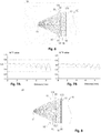
- Fig. 1 is a schematic view of a near-eye light field display device in accordance with an embodiment of the invention.
- the near-eye light field display device 10 of the embodiment includes a display element 15, a micro lens array 13 and an optical element 11.
- the display element 15 includes a plurality of micro-image units 151.
- Each of the micro-image units 151 is used for providing an elemental image beam LS ( Fig. 1 is schematically illustrated with the upper boundary of the elemental image beam LS emitted from the micro-image unit 151 located on the upper edge and the lower boundary of the elemental image beam LS emitted from the micro-image unit 151 located on the lower edge as examples).
- the micro lens array 13 is disposed in front of the display element 15 and has a plurality of microlenses 131.
- the microlenses 131 correspond to the micro-image units 151 of the display element 15, respectively.
- the optical element 11 is disposed in front of the microlens array 13 and is located on the transmission path of the elemental image beams LS from the microlenses 131.
- the microlens array 13 is located between the optical element 11 and the display element 15, and each of the elemental image beams LS is projected toward the optical element 11 through the corresponding microlens 131.
- the Abbe number of the microlens array 13 is denoted by Vd MLA
- the refractive index of the microlens array 13 is denoted by nd MLA
- the Abbe number of the optical element 11 is denoted by Vd OE
- the refractive index of the optical element 11 is denoted by nd OE .
- the material of each microlens 131 is identical, for example, such that the Abbe number of the microlens array 13 is equal to the Abbe number of each microlens131, and the refractive index of the lens array 13 is equal to the refractive index of each microlens 131, for example.
- the microlens array 13 and the optical element 11 meet at least one of the conditions: Vd OE >Vd MLA and nd OE ⁇ nd MLA .
- the aberration can be eliminated with the configuration in which the optical element 11 and the microlens array 13 are different in material, so as to achieve a clear image with high quality.
- the optical element 11 is a biconvex lens for example, but the invention is not limited thereto.
- each of the micro-image units 151 of the display element 15 includes, for example, a plurality of pixels (not shown) used for providing the elemental image beam LS.
- Each of the image beams LS is projected to the optical element 11 via the corresponding microlens 131.
- the optical element 11 is used for collecting the elemental image beams LS projected through the microlenses 131 and transmitting the elemental image beams LS to the eyes EY of the user.
- the eyes EY of the user may see a light field virtual image S0 shown as like far away, and thus the user can see a light field image which may be perceived in depth direction.
- Fig. 2A is a schematic view of a plurality of elemental images respectively displayed by a plurality of micro-image units of a display element of the near-eye light field display device in the embodiment shown in Fig. 1.
- Fig. 2B is a schematic view of an image observed by the user's eyes through the near-eye light field display device of the embodiment shown in Fig. 1 .
- the elemental images EI0 and EI shown in Fig. 2A are examples formed by the elemental image beams LS provided by the micro-image units 151 of the display element 15. As shown in Fig.
- a plurality of the micro-image units 151 display one elemental image EI0 and a plurality of elemental images EI, wherein the elemental image EI0 is defined as a central elemental image and the plurality of elemental images EI surround the central elemental image (i.e., elemental image EI0).
- each of the elemental images EI0 and EI is projected to the optical element 11 via the corresponding microlens 131 and then projected to the eyes EY of the user via the optical element 11, so that the user can see the image as shown in Fig. 2B .
- the user may see a light field image which may be perceived in depth direction.
- the elemental images EI0 and EI generated by the display element 15 shown in Fig. 2A are illustrated by way of example, and the invention is not limited thereto.
- Fig. 3 is a schematic view of a microlens array of the near-eye light field display device of the embodiment shown in Fig. 1 .
- the plurality of microlenses 131 of the microlens array 13 are arranged in a matrix for example, but the invention is not limited thereto.
- the focal length of each microlens 131 is identical for example.
- the focal lengths of the microlenses 131 may be different. For example, as shown in Fig.
- the plurality of microlenses 131 may have different focal lengths which vary gradually along the directions from the central microlens 131 to the leftmost or the rightmost microlens 131.
- the plurality of microlenses 131 may have different focal lengths which vary gradually along the directions from the central microlens 131 to the upmost or the lowmost microlens 131.
- the various focal lengths may increase gradually in value along the directions from the center to the left or right, or along the directions from the center to the top or bottom, but the invention is not limited thereto.
- the various focal lengths may first increase and then reduce in value, but the invention is not limited thereto.
- the various focal lengths may vary in different ways as required by different designs.
- the image projection may be tuned finely, so as to achieve a clearer image with high quality.
- the optical element 11 may cause the elemental image beam LS to turn by a significant angle, so that the microlenses 131 of the micro lens array 13 may not need to adopt the special design of the inclined optical surface. That is, a general microlens array design without inclined optical surfaces can be adopted to improve the convenience and yield during manufacturing/process and further to avoid breakages between the optical surfaces of adjacent microlenses.
- the near-eye light field display device 10 of the embodiment can alleviate /solve the problems of reduced amount of incident light and reduced effective area of microlens (or, reduced effective aperture) caused by the conventional near-eye light field display device which uses a microlens array with the optical surfaces having the breakages.
- the near-eye light field display device 10 of the embodiment can improve the imaging quality.
- the incident angle ⁇ 1 of the elemental image beam LS entering the user's eyes EY may be much greater than the exit angle ⁇ 2 of the elemental image beam LS emitted from the micro-image unit 151. Therefore, the near-eye light field display device 10 can achieve a large field of view without a great overall thickness.
- the design of the optical element of the invention is not limited to Fig. 1 .
- Other embodiments of the near-eye light field display device using different optical elements will be described below, but the invention is not limited to the following embodiments.
- Fig. 4A is a schematic view of a near-eye light field display device in accordance with another embodiment of the invention.
- the near-eye light field display device 20 includes a display element 15, a microlens array 23 and an optical element 21.
- the near-eye light field display device 20 of the embodiment has a similar structure and function as the near-eye light field display device 10 shown in Fig. 1 .
- the embodiment shown in Fig. 4A is different from the embodiment shown in Fig.
- the optical element 21 has a first surface S3 and a second surface S2, the first surface S3 is adjacent to the microlens array 23, the second surface S2 is away from the microlens array 23, the first surface S3 is located between the second surface S2 and the microlens array 23, the first surface S3 is a convex surface, and the second surface S2 is a plane surface.
- the optical element 21 of the embodiment is a planoconvex lens, wherein the convex surface (first surface S3) is located between the plane surface (second surface S2) and the microlens array 23.
- the first surface S3 may be a spherical surface or an aspherical surface, and the invention is not limited thereto.
- the structure of the microlens array 23 in the embodiment is similar to that in Fig. 3 and may be constituted by a plurality of microlenses 231 having identical or different focal lengths.
- the spacing in Table 1 indicates the linear distance between two adjacent surfaces along the optical axis of the near-eye light field display device 20.
- the spacing of the surface S1 indicates the linear distance between the surface S1 and the surface S2 along the optical axis.
- the spacing of the surface S0 is -1000 mm, which indicates that the light field virtual image is located 1000 mm in front of the pupil.
- the surface having a positive radius of curvature means that the surface is curved toward the left side of the figure, and the surface having a negative radius of curvature means that the surface is curved toward the right side of the figure.
- Z is denoted as the coordinate value in the direction of the optical axis Ax; k is denoted as a conic constant; R is denoted as the radius of curvature; Y is denoted as the coordinate value along the direction orthogonal to the optical axis Ax, that is, the radial height of the aspherical surface SA, wherein the positive direction of Y is defined as the direction toward the top of the figure; and B, C, D, E, F, G, H and K are denoted as the aspheric coefficients.
- Tables 1 and 2 the aspherical coefficients B, G, H, I, J and K are omitted since they are all 0.
- Parameters associated with of the aspherical micro lenses 231 are shown in Table 2.
- Table 2 Surface k C D E F S3 -3.174 -3.2E-5 3.151E-8 -1.769E-9 1.492E-11 S4 6.722 -1.182E-1 -4.78E-3 -2.511E-1 3.485E-1 S5 3.34 1.124E-1 7.596E-1 -2.293 6.463
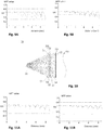
- Fig. 5A shows a chart of a modulation transfer function (MTF) generated by using the near-eye light field display device of Fig. 4A in which each microlens of the microlens array has an identical focal length (e.g., 3.392 mm).
- the horizontal axis represents the distance (unit: mm) between the elemental image EI and the elemental image EI0 (i.e., the center elemental image)
- the vertical axis represents the MTF value
- the solid-line is the MTF curve in the sagittal direction
- the dashed line is the MTF curve in the tangential direction.
- the microlenses 231 of the micro lens array 23 of the near-eye light field display device 20 in Fig. 4A may have different focal lengths.
- Fig. 5B shows a chart of a modulation transfer function generated by using the near-eye light field display device of Fig. 4A in which the microlenses of the microlens array have different focal lengths (e.g., the effective focal length (EFL) in Table 5).
- EFL effective focal length
- the aspherical coefficients B, G, H, I, J and K are omitted since they are all 0.
- the radius of curvature of the surface S5 of the microlens array 23 in Table 3 is represented by the radius of curvature at the center of the microlens array 23.
- the distance in Table 5 indicates the distance between the center of the microlens 231 and the center of the microlens array 23 and corresponds to the distance between the elemental image EI and the elemental image EI0 (i.e., central elemental image) indicated by the horizontal axis in Fig. 5B
- the effective focal length in Table 5 indicates the focal length of the micro lens 231.
- Fig. 6 is a schematic view of a near-eye light field display device in accordance with another embodiment of the invention.
- the near-eye light field display device 30 includes a display element 15, a microlens array 33 and an optical element 31.
- the near-eye light field display device 30 of the embodiment has a similar structure and function as the near-eye light field display device 10 shown in Fig. 1 .
- the embodiment shown in Fig. 6 is different from the embodiment shown in Fig.
- the optical element 31 has a first surface S3 and a second surface S2, the first surface S3 is adjacent to the microlens array 33, the second surface S2 is away from the microlens array 33, the first surface S3 is located between the second surface S2 and the microlens array 33, the first surface S3 is a plane surface, and the second surface S2 is a convex surface.
- the optical element 31 of the embodiment is a planoconvex lens, wherein the plane surface (first surface S3) is located between the convex surface (second surface S2) and the microlens array 33.
- the second surface S2 may be a spherical surface or an aspherical surface, and the invention is not limited thereto.
- the structure of the microlens array 33 in the embodiment is similar to that in Fig. 3 and may be constituted by a plurality of micro lenses 331 having identical or different focal lengths.
- Fig. 7A shows a chart of a modulation transfer function generated by using the near-eye light field display device of Fig. 6 in which each microlens of the microlens array has an identical focal length (e.g., 3.304 mm).
- the microlenses 331 of the microlens array 33 of the near-eye light field display device 30 in Fig. 6 may have different focal lengths.
- Fig. 7B shows a chart of a modulation transfer function generated by using the near-eye light field display device of Fig.
- the aspherical coefficient B in Table 9-1 is 0 for example.
- the aspherical coefficients B, G, H, I, J and K are omitted since they are all 0.
- the radius of curvature of the surface S5 of the microlens array 33 in Table 8 is represented by the radius of curvature at the center of the microlens array 33.
- Table 8 Position Surface Radius of curvature (mm) Spacing (mm) Refractive index Abbe number Light field virtual image S0 Infinity -1000 Pupil S1 Infinity 13.49 Optical element S2 30.735 2.158 1.533 55.732 S3 Infinity 0.2 Microlens array S4 -2.621 1 1.59 29.921 S5 -1.267 3.5 Display element S6 Table 9-1 Surface k C D E F S2 -15.582 9.109E-5 -1.174E-6 1.531E-8 -1.099E-10 S4 5.664 -0.114 -1.16E-1 0.06 0 S5 2.885 0.114 8.67E-1 -2.689 7.113 Table 9-2 Surface G H I J K S2 3.246E-13 2.246E-15 -4.146E-17 -9.235E-19 1.33E-20 S4 0 0 0 0 0 S5 0 0 0 0 0 Table 10 Distance (mm) Radius of curvature (mm) k C D E F Effective focal
- Fig. 8 is a schematic view of a near-eye light field display device in accordance with another embodiment of the invention.
- the near-eye light field display device 40 includes a display element 15, a micro lens array 43 and an optical element 41.
- the near-eye light field display device 40 of the embodiment has a similar structure and function as the near-eye light field display device 10 shown in Fig. 1 .
- the embodiment shown in Fig. 8 is different from the embodiment shown in Fig.
- the optical element 41 has a first surface S3 and a second surface S2, the first surface S3 is adjacent to the microlens array 43, the second surface S2 is away from the microlens array 43, the first surface S3 is located between the second surface S2 and the microlens array 43, the first surface S3 is a convex surface, and the second surface S2 is a concave surface.
- the optical element 41 of the embodiment is a lens having a double-sided curvature.
- the first surface S3 may be a spherical surface or an aspherical surface
- the second surface S2 may be a spherical surface or an aspherical surface, and the invention is not limited thereto.
- the structure of the microlens array 43 in the embodiment is similar to that in Fig. 3 and may be constituted by a plurality of microlenses 431 having identical or different focal lengths.
- Fig. 9A shows a chart of a modulation transfer function generated by using the near-eye light field display device of Fig. 8 in which each microlens of the microlens array has the same focal length (e.g., 3.333 mm).
- the microlenses 431 of the microlens array 43 of the near-eye light field display device 40 in Fig. 8 may have different focal lengths. Please refer to the related parameters in Tables 13, 14, 15 and Fig. 9B.
- Fig. 9B shows a chart of a modulation transfer function generated by using the near-eye light field display device of Fig.
- the microlenses of the microlens array have different focal lengths (e.g., the effective focal lengths in Table 15).
- the aspherical coefficients B, G, H, I, J and K are omitted since they are all 0.
- the radius of curvature of the surface S5 of the microlens array 43 shown in Table 13 is represented by the radius of curvature at the center of the microlens array 43.
- Fig. 10 is a schematic view of a near-eye light field display device in accordance with another embodiment of the invention.
- the near-eye light field display device 50 includes a display element 15, a microlens array 53 and an optical element 51.
- the near-eye light field display device 50 of the embodiment has a similar structure and function as the near-eye light field display device 10 shown in Fig. 1 .
- the embodiment shown in Fig. 10 is different from the embodiment shown in Fig.
- the optical element 51 has a first surface S3 and a second surface S2, the first surface S3 is adjacent to the microlens array 53, the second surface S2 is away from the microlens array 53, the first surface S3 is located between the second surface S2 and the microlens array 53, the first surface S3 is a diffractive optical element (DOE) surface, and the second surface S2 is a convex surface.
- the diffractive optical element surface (the first surface S3) can effectively reduce color difference.
- the first surface S3 may be a spherical surface or an aspherical surface, and the invention is not limited thereto.
- the structure of the microlens array 53 in the embodiment is similar to that in Fig. 3 and may be constituted by a plurality of micro lenses 531 having identical or different focal lengths.
- Fig. 11A shows a chart of a modulation transfer function generated by using the near-eye light field display device of Fig. 10 in which each microlens of the microlens array has the same focal length (e.g., 3.241 mm).
- the microlenses 531 of the microlens array 53 of the near-eye light field display device 50 in Fig. 10 may have different focal lengths. Please refer to the related parameters in Tables 19, 20, 21-1, 21-2, 22 and Fig. 11B.
- Fig. 11B shows a chart of a modulation transfer function generated by using the near-eye light field display device of Fig.
- the microlenses of the microlens array have different focal lengths (e.g., the effective focal lengths in Table 22).
- the aspherical coefficients B, G, H, I, J and K are omitted since they are all 0.
- the radius of curvature of the surface S5 of the microlens array 53 shown in Table 19 is represented by the radius of curvature at the center of the microlens array 53.
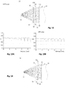
- Fig. 12 is a schematic view of a near-eye light field display device in accordance with another embodiment of the invention.
- the near-eye light field display device 60 includes a display element 15, a microlens array 63 and an optical element 61.
- the near-eye light field display device 60 of the embodiment has a similar structure and function as the near-eye light field display device 10 shown in Fig. 1 .
- the embodiment shown in Fig. 12 is different from the embodiment shown in Fig.
- the optical element 61 has a first surface S3 and a second surface S2, the first surface S3 is adjacent to the microlens array 63, the second surface S2 is away from the microlens array 63, the first surface S3 is located between the second surface S2 and the microlens array 63, the first The surface S3 is a convex surface, and the second surface S2 is a diffractive optical element surface.
- the diffractive optical element surface (the first surface S3) can effectively reduce color difference.
- the first surface S3 may be a spherical surface or an aspherical surface, and the invention is not limited thereto.
- the structure of the microlens array 63 in the embodiment is similar to that in Fig. 3 and may be constituted by a plurality of micro lenses 631 having identical or different focal lengths.
- Fig. 13A shows a chart of a modulation transfer function generated by using the near-eye light field display device of Fig. 12 in which each microlens of the microlens array has the same focal length (e.g., 3.287 mm).
- the microlenses 631 of the microlens array 63 of the near-eye light field display device 60 in Fig. 12 may have different focal lengths. Please refer to the related parameters in Tables 26, 27, 28, 29 and Fig. 13B.
- Fig. 13B shows a chart of a modulation transfer function generated by using the near-eye light field display device of Fig.
- the microlenses of the microlens array have different focal lengths (e.g., the effective focal lengths shown in Table 29).
- the aspherical coefficients B, G, H, I, J and K are omitted since they are all 0.
- the radius of curvature of the surface S5 of the microlens array 63 in Table 26 is represented by the radius of curvature at the center of the microlens array 63.
- Fig. 14 is a schematic view of a near-eye light field display device in accordance with another embodiment of the invention.
- the near-eye light field display device 70 includes a display element 15, a microlens array 73 and an optical element 71.
- the near-eye light field display device 70 of the embodiment has a similar structure and function as the near-eye light field display device 10 shown in Fig. 1 .
- the embodiment shown in Fig. 14 is different from the embodiment shown in Fig.
- the optical element 71 has a first surface S3 and a second surface S2, the first surface S3 is adjacent to the microlens array 73, the second surface S2 is away from the micro lens array 73, the first surface S3 is located between the second surface S2 and the microlens array 73, the first Surface S3 is a Fresnel lens surface, and the second surface S2 is a diffractive optical element surface.
- the Fresnel lens surface (the first surface S3) can effectively reduce the lens thickness
- the diffractive optical element surface (the second surface S2) can effectively reduce the color difference.
- the structure of the microlens array 73 in the embodiment is similar to that in Fig. 3 and may be constituted by a plurality of micro lenses 731 having identical or different focal lengths.
- Fig. 15A shows a chart of a modulation transfer function generated by using the near-eye light field display device of Fig. 14 in which each microlens of the microlens array has the same focal length (e.g., 3.302 mm).
- the microlenses 731 of the microlens array 73 of the near-eye light field display device 70 in Fig. 14 may have different focal lengths. Please refer to the related parameters in Tables 33, 34, 35, 36 and Fig. 15B.
- Fig. 15B shows a chart of a modulation transfer function generated by using the near-eye light field display device of Fig.
- the microlenses of the microlens array have different focal lengths (e.g., the effective focal lengths shown in Table 36).
- the aspherical coefficients B, G, H, I, J and K are omitted since they are all 0.
- the radius of curvature of the surface S5 of the microlens array 73 in Table 33 is represented by the radius of curvature at the center of the microlens array 73.
- Fig. 16 is a schematic view of a near-eye light field display device in accordance with another embodiment of the invention.
- the near-eye light field display device 80 includes a display element 15, a microlens array 13, an optical element 11 and a light redirecting element 81.
- the near-eye light field display device 80 of the embodiment has a similar structure and function as the near-eye light field display device 10 shown in Fig. 1 .
- the embodiment shown in Fig. 16 is different from the embodiment shown in Fig. 1 in that the near-eye light field display device 80 further includes a light redirecting element 81.
- the elemental image beam (not shown) becomes the image beam L1 after passing through the optical element 11.
- the light redirecting element 81 is located on the transmission path of the image beam L1 from the optical element 11 and is disposed on a side of the optical element 11 away from the micro lens array 13. In the embodiment, the optical element 11 is located between the light redirecting element 81 and the micro lens array 13. In the embodiment, the image beam L1 is reflected by the light redirecting element 81 and then directed toward the user's eyes EY (the image beam L2).
- the light redirecting element 81 may be a partially-penetrating-and-partially-reflecting element for example. Therefore, light beam LA from the external ambient light source can penetrate the light redirecting element 81 to the user's eyes EY, so that the near-field light field display device 80 of the embodiment can be applied to a virtual reality application or the like, for example.
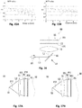
- Figs. 17A and 17B are schematic views of a near-eye display device in different zooming states in accordance with an embodiment of the invention.
- the near-eye display device 90 of the embodiment includes a display element 95, a micro lens array 93 and an optical element 91.
- the near-eye display device 90 is, for example, a near-eye light field display device.
- the display device 95 has a plurality of micro-image units 951. Each of the micro-image units 951 is used for providing an elemental image beam LS ( Figs.
- the microlens array 93 is disposed in front of the display element 95 and has a plurality of micro lenses 931.
- the microlenses 931 correspond to the micro-image units 951, respectively.
- the optical element 91 is disposed in front of the microlens array 3 and is located on the transmission path of the elemental image beams LS from the microlenses 931.
- the microlens array 93 is located between the optical element 91 and the display element 95, and each of the elemental image beams LS is projected toward the optical element 91 through the corresponding microlens 931.
- the optical element 91 has an adjustable focal length.
- the display element 95 and the microlens array 93 are similar to the display element 15 and the microlens array 13 shown in Fig. 1 respectively, and not described in detail.
- the optical element 91 of the embodiment is, for example, a liquid lens, a liquid crystal lens or other optical elements with an adjustable focal length.
- the elemental image beam LS can be turned by a large angle due to the use of the optical element 91, the incident angle ⁇ 3 of the elemental image beam LS entering the user's eyes EY (i.e., the surface S1 in Figs. 17A and 17B ) may be much greater than the exit angle ⁇ 4 of the elemental image beam LS emitted from the micro-image unit 951. Therefore, the near-eye display device 90 can achieve a large field of view without a great overall thickness.
- the near-eye display device 90 has the focus accommodation function, such that the field of view and angular resolution can be changed by adjusting the focal length of the optical element 91.
- the focal length of the optical element 91 in Fig. 17A is longer than that of the optical element 91in Fig. 17B
- the field of view of the light field virtual image S0 in Fig. 17A is narrower than that of the light field virtual image S0 in Fig. 17B
- the exit angle ⁇ 4 shown in Fig. 17A is larger than that shown in Fig. 17B .
- the difference in the shapes of the optical elements 91 is schematically shown to illustrate the difference in focal lengths for the benefit of clarity, rather than to specifically limit the shape of the optical element 91.
- Figs. 18A and 18B are schematic views of a near-eye display device in different zooming states in accordance with another embodiment of the invention.
- the near-eye display device 100 of the embodiment includes a display element 95, a microlens array 103 and an optical element 101.
- the near-eye display device 100 in the embodiment has a similar structure and function to the near-eye display device 90 and the difference is that the microlens array 103 in the embodiment has an adjustable focal length, that is, each microlens 1031 of the microlens array 103 in the embodiment has an adjustable focal length. Adjusting the focal length of the microlens array 103 means adjusting the focal lengths of the microlenses 1031.
- each microlens 1031 is, for example, a liquid lens, a liquid crystal lens or other optical elements with an adjustable focal length.
- the near-eye display device 100 may include a near-eye light field display device and may also include a near-eye display device without the function of light-field display.
- the microlens array 103 has a certain refractive power such that the near-eye display device 100 may form a light field virtual image S0 having a depth of field.
- the focal length of the microlens array 103 is adjusted to infinity (i.e., zero refractive power) for example, so that the virtual image S01 formed by the near-eye display device 100 may have no depth of field.
- the near-eye display device 100 can be switched to a near-eye light field display device or a near-eye display device without the function of light field display so as to improve the versatility and convenience during use.
- Figs. 19A and 19B are schematic views of a near-eye display device in different zooming states in accordance with another embodiment of the invention.
- the near-eye display device 110 of the embodiment includes a display element 95, a microlens array 113 and an optical element 111.
- the near-eye display device 110 in the embodiment has a similar structure and function to the near-eye display device 100 and the difference is that the optical element 111 of the embodiment does not have an adjustable focal length.
- the microlens array 113 has an adjustable focal length, that is, each microlens 1131 of the microlens array 113 has an adjustable focal length.
- Each microlens 1131 may be a liquid lens, a liquid crystal lens or other optical elements with an adjustable focal length.
- the field of view and the angular resolution may be changed by adjusting the focal length of the micro lens array 113.
- the microlens array 113 has a certain refractive power, such that the near-eye display device 110 may form a light field virtual image S0 having a depth of field.
- the focal length of the microlens array 113 is adjusted to infinity (i.e., zero refractive power) for example, so that the virtual image S01 formed by the near-eye display device 110 may have no depth of field.
- the near-eye display device 110 can be switched to a near-eye light field display device or a near-eye display device without the function of light field display, so as to improve the versatility and convenience during use.
- the microlens array 113 has an adjustable focal length and the focal length of the microlens array 113 in Fig. 19A is shorter than that in Fig. 19B , the exit angle ⁇ 4 in Fig. 19A is smaller than that in Fig. 19B .
- the difference in the shapes of the microlens arrays 113 is schematically shown to illustrate the difference in focal lengths for the benefit of clarity, rather than to specifically limit the shape of the microlens array 113.
- the Abbe number of the microlens arrays 93, 103, 113 is denoted by Vd MLA
- the refractive index of the microlens arrays 93, 103, 113 is denoted by nd MLA
- the Abbe number of the optical elements 91, 101, 111 is denoted by Vd OE
- the refractive index of the optical elements 91, 101, 111 is denoted by nd OE .
- the relationship between the values of Vd MLA and Vd OE , and the relationship between the values of nd MLA and nd OE may be set as required by different designs.
- the microlens arrays 93, 103, 113 and the respective optical elements 91, 101, 111 meet at least one of the conditions: Vd OE >Vd MLA and nd OE ⁇ nd MLA .
- the microlens arrays 93, 103, 113 and the respective optical elements 91, 101, 111 meet at least one of the conditions: Vd OE ⁇ Vd MLA and nd OE >nd MLA .
- the near-eye light field display device of the embodiment of the invention can achieve a reduced thickness and weight of the near-eye light field display device and an improved field of view.
- the near-eye display device in the embodiment of the invention has a function of focus accommodation and can change the field of view and the angular resolution.
Landscapes
- Physics & Mathematics (AREA)
- General Physics & Mathematics (AREA)
- Optics & Photonics (AREA)
- Engineering & Computer Science (AREA)
- Multimedia (AREA)
- Signal Processing (AREA)
- Diffracting Gratings Or Hologram Optical Elements (AREA)
- Testing, Inspecting, Measuring Of Stereoscopic Televisions And Televisions (AREA)
- Devices For Indicating Variable Information By Combining Individual Elements (AREA)
Abstract
Description
- THIS APPLICATION CLAIMS PRIORITY OF
CN201710910334.6, FILED ON 2017/09/29 - The invention relates to a display device, and more particularly to a near-eye light field display device.
- Near-eye light field display device is a display device using light field display technology to produce stereoscopic images. A real image is formed on an imaging surface by a light filed image display device with a microlens array such that an observer can see a light field image which may be perceived in depth direction and shown as like far away.
- However, the conventional near-eye light field display devices generally use a freeform prism or a multi-piece eyepiece for imaging, causing the conventional near-eye light field display devices thick, heavy, and thus not suitable for long time wearing. Moreover, the freeform prisms are generally made of plastic materials, and its optical material has a lower Abbe number and the dispersion is more serious. Further, if a wider field of view (FOV) of the near-eye light field display devices is desired, the thickness and weight of the freeform prism or the multi-piece eyepiece would be increased accordingly, causing a limited field of view for the conventional near-field light field display devices. Therefore, how to reduce the thickness and weight of the near-field light field display device while improving the field of view is actually a focus of attention for the persons in the field of the art.
- The information disclosed in this "BACKGROUND OF THE INVENTION" section is only for enhancement understanding of the background of the invention and therefore it may contain information that does not form the prior art that is already known to a person of ordinary skill in the art. Furthermore, the information disclosed in this "BACKGROUND OF THE INVENTION" section does not mean that one or more problems to be solved by one or more embodiments of the invention were acknowledged by a person of ordinary skill in the art.
- The invention provides a near-eye light field display device configured to reduce the thickness and weight while improving the field of view.
- The invention further provides a near-eye display device configured to reduce the thickness and weight and improve the field of view while the depth of field being adjustable.
- Other objectives and advantages of the invention can be further understood from the technical features disclosed in the invention.
- In order to achieve one or a part or all of the above objectives or other objectives, an embodiment of the invention provides a near-eye light field display device, which includes a display element, a microlens array and an optical element. The display element has a plurality of micro-image units. Each of the micro-image units is configured to provide an elemental image beam. The microlens array is disposed in front of the display element and has a plurality of microlenses. The microlenses correspond to the micro-image units respectively. The optical element is disposed in front of the microlens array and located on a transmission path of the elemental image beams from the microlenses. The microlens array is located between the optical element and the display element. Each of the elemental image beams passes through the corresponding microlens and is projected toward the optical element.
- Preferably, an Abbe number of the microlens array is VdMLA, a refractive index of the microlens array is ndMLA, an Abbe number of the optical element is VdOE, a refractive index of the optical element is ndOE, and the microlens array and the optical element meet at least one of conditions: VdOE>VdMLA and ndOE <ndMLA.
- In order to achieve one or a part or all of the above objectives or other objectives, another embodiment of the invention provides a near-eye display device, which includes a display element, a microlens array and an optical element. The display element has a plurality of micro-image units. Each of the micro-image units is configured to provide an elemental image beam. The microlens array is disposed in front of the display element and has a plurality of microlenses. The microlenses correspond to the micro-image units respectively. The optical element is disposed in front of the microlens array and located on a transmission path of the elemental image beams from the microlenses. The microlens array is located between the optical element and the display element. Each of the elemental image beams passes through the corresponding microlens and is projected toward the optical element. At least one of the microlens array and the optical element has an adjustable focal length.
- In summary, with an optical element disposed in front of the microlens array and they both meeting at least one of the following conditions: VdOE>VdMLA and ndOE<ndMLA, the near-eye light field display devices of the embodiments of the invention can achieve a reduced thickness and weight and an improved field of view. In addition, since at least one of the microlens array and the optical element has an adjustable focal length, the near-eye display device in the embodiment of the invention has a function of focus accommodation and can change the field of view and the angular resolution.
- In some embodiments the near-eye light display device is a near-eye light field display device,
- Preferably, an Abbe number of the microlens array is VdMLA, a refractive index of the microlens array is ndMLA, an Abbe number of the optical element is VdOE, a refractive index of the optical element is ndOE, and the microlens array and the optical element meet at least one of conditions: VdOE>VdMLA, and ndOE <ndMLA.
- Preferably, the optical element has a first surface and a second surface, the first surface is adjacent to the microlens array, and the second surface is away from the microlens array, wherein the first surface is a convex surface, and the second surface is a plane surface, and wherein the first surface is a spherical surface or an aspherical surface.
- Preferably, the optical element has a first surface and a second surface, the first surface is adjacent to the microlens array, and the second surface is away from the microlens array, wherein the first surface is a plane surface, and the second surface is a convex surface, and wherein the second surface is a spherical surface or an aspherical surface.
- Preferably, the optical element has a first surface and a second surface, the first surface is adjacent to the microlens array, and the second surface is away from the microlens array, wherein the first surface has a convex surface, and the second surface has a concave surface, and wherein the first surface is a spherical surface or an aspherical surface, and the second surface is a spherical surface or an aspherical surface.
- Preferably, the optical element has a first surface and a second surface, the first surface is adjacent to the micro lens array, and the second surface is away far from the microlens array, wherein the first surface is a diffractive optical element surface, and the second surface is a convex surface, and wherein the second surface is a spherical surface or an aspherical surface.
- Preferably, the optical element has a first surface and a second surface, the first surface is adjacent to the microlens array, and the second surface is away from the microlens array, wherein the first surface is a convex surface, and the second surface is a diffractive optical element surface, and wherein the first surface is a spherical surface or an aspherical surface.
- Preferably, the optical element has a first surface and a second surface, the first surface is adjacent to the microlens array, and the second surface is away from the microlens array, and wherein the first surface is a Fresnel lens surface, and the second surface is a diffractive optical element surface.
- Preferably, the near-eye light display device further comprises a light redirecting element, wherein the elemental image beams are converted into image beams after passing through the optical element, and the light redirecting element is located on a transmission path of the image beams from the optical element.
- Preferably, the light redirecting element is a partially-penetrating-and-partially-reflecting element.
- Preferably, focal lengths of the plurality of microlenses are identical.
- Preferably, the focal lengths of the plurality of microlenses are different.
- Preferably, the microlens array has an adjustable focal length and/or the optical element has an adjustable focal length.
- Preferably, an Abbe number of the microlens array is VdMLA, a refractive index of the microlens array is ndMLA, an Abbe number of the optical element is VdOE, a refractive index of the optical element is ndOE, and the microlens array and the optical element meet y at least one of conditions: VdOE<VdMLA and ndOE>ndMLA.
- Preferably, an Abbe number of the microlens array is VdMLA, a refractive index of the microlens array is ndMLA, an Abbe number of the optical element is VdOE, a refractive index of the optical element is ndOE, and the microlens array and the optical element meet at least one of conditions: VdOE=VdMLA and ndOE=ndMLA.
- Other objectives, features and advantages of the present invention will be further understood from the further technology features disclosed by the embodiments of the present invention, wherein preferred embodiments of this invention are shown and described by way of illustration of modes best suited to carry out the invention.
- The accompanying drawings are included to provide a further understanding of the invention, and are incorporated in and constitute a part of this specification. The drawings illustrate embodiments of the invention and, together with the description, serve to explain the principles of the invention.
-
Fig. 1 is a schematic view of a near-eye light field display device in accordance with an embodiment of the invention; -
Fig. 2A is a schematic view of a plurality of elemental images respectively displayed by a plurality of micro-image units of a display element of the near-eye light field display device in the embodiment shown inFig. 1 ; -
Fig. 2B is a schematic view of an image observed by the user's eyes through the near-eye light field display device of the embodiment shown inFig. 1 ; -
Fig. 3 is a schematic view of a micro lens array of the near-eye light field display device of the embodiment shown inFig. 1 ; -
Fig. 4A is a schematic view of a near-eye light field display device in accordance with another embodiment of the invention; -
Fig. 4B is a schematic view of the radial height of an aspherical surface; -
Fig. 5A shows a chart of a modulation transfer function (MTF) generated by using the near-eye light field display device ofFig. 4A , wherein each microlens of the microlens array has an identical focal length; -
Fig. 5B shows a chart of a modulation transfer function generated by using the near-eye light field display device ofFig. 4A , wherein the microlenses of the microlens array have different focal lengths; -
Fig. 6 is a schematic view of a near-eye light field display device in accordance with another embodiment of the invention; -
Fig. 7A shows a chart of a modulation transfer function generated by using the near-eye light field display device ofFig. 6 , wherein each microlens of the microlens array has an identical focal length; -
Fig. 7B shows a chart of a modulation transfer function generated by using the near-eye light field display device ofFig. 6 , wherein the microlenses of the microlens array have different focal lengths; -
Fig. 8 is a schematic view of a near-eye light field display device in accordance with another embodiment of the invention; -
Fig. 9A shows a chart of a modulation transfer function generated by using the near-eye light field display device ofFig. 8 , wherein each microlens of the microlens array has an identical focal length; -
Fig. 9B shows a chart of a modulation transfer function generated by using the near-eye light field display device ofFig. 8 , wherein the microlenses of the microlens array have different focal lengths; -
Fig. 10 is a schematic view of a near-eye light field display device in accordance with another embodiment of the invention; -
Fig. 11A shows a chart of a modulation transfer function generated by using the near-eye light field display device ofFig. 10 , wherein each microlens of the microlens array has an identical focal length; -
Fig. 11B shows a chart of a modulation transfer function generated by using the near-eye light field display device ofFig. 10 , wherein the microlenses of the microlens array have different focal lengths; -
Fig. 12 is a schematic view of a near-eye light field display device in accordance with another embodiment of the invention; -
Fig. 13A shows a chart of a modulation transfer function generated by using the near-eye light field display device ofFig. 12 , wherein each microlens of the microlens array has an identical focal length; -
Fig. 13B shows a chart of a modulation transfer function generated by using the near-eye light field display device ofFig. 12 , wherein the microlenses of the microlens array have different focal lengths; -
Fig. 14 is a schematic view of a near-eye light field display device in accordance with another embodiment of the invention; -
Fig. 15A shows a chart of a modulation transfer function generated by using the near-eye light field display device ofFig. 14 , wherein each microlens of the microlens array has an identical focal length; -
Fig. 15B shows a chart of a modulation transfer function generated by using the near-eye light field display device ofFig. 14 , wherein the microlenses of the microlens array have different focal lengths; -
Fig. 16 is a schematic view of a near-eye light field display device in accordance with another embodiment of the invention; -
Figs. 17A and 17B are schematic views of a near-eye display device in different zooming states in accordance with an embodiment of the invention; -
Figs. 18A and 18B are schematic views of a near-eye display device in different zooming states in accordance with another embodiment of the invention; and -
Figs. 19A and 19B are schematic views of a near-eye display device in different zooming states in accordance with another embodiment of the invention. - In the following detailed description of the preferred embodiments, reference is made to the accompanying drawings which form a part hereof, and in which is shown by way of illustration specific embodiments in which the invention may be practiced. In this regard, directional terminology, such as "top", "bottom", "front", "back", etc., is used with reference to the orientation of the Figure(s) being described. The components of the invention can be positioned in a number of different orientations. As such, the directional terminology is used for purposes of illustration and is in no way limiting. On the other hand, the drawings are only schematic and the sizes of components may be exaggerated for clarity. It is to be understood that other embodiments may be utilized and structural changes may be made without departing from the scope of the invention. Also, it is to be understood that the phraseology and terminology used herein are for the purpose of description and should not be regarded as limiting. The use of "including", "comprising", or "having" and variations thereof herein is meant to encompass the items listed thereafter and equivalents thereof as well as additional items. Unless limited otherwise, the terms "connected", "coupled", and "mounted" and variations thereof herein are used broadly and encompass direct and indirect connections, couplings, and mountings. Similarly, the terms "facing," "faces" and variations thereof herein are used broadly and encompass direct and indirect facing, and "adjacent to" and variations thereof herein are used broadly and encompass directly and indirectly "adjacent to". Therefore, the description of "A" component facing "B" component herein may contain the situations that "A" component directly faces "B" component or one or more additional components are between "A" component and "B" component. Also, the description of "A" component "adjacent to" "B" component herein may contain the situations that "A" component is directly "adjacent to" "B" component or one or more additional components are between "A" component and "B" component. Accordingly, the drawings and descriptions will be regarded as illustrative in nature and not as restrictive.
-
Fig. 1 is a schematic view of a near-eye light field display device in accordance with an embodiment of the invention. Referring toFig. 1 , the near-eye lightfield display device 10 of the embodiment includes adisplay element 15, amicro lens array 13 and anoptical element 11. Thedisplay element 15 includes a plurality ofmicro-image units 151. Each of themicro-image units 151 is used for providing an elemental image beam LS (Fig. 1 is schematically illustrated with the upper boundary of the elemental image beam LS emitted from themicro-image unit 151 located on the upper edge and the lower boundary of the elemental image beam LS emitted from themicro-image unit 151 located on the lower edge as examples). Themicro lens array 13 is disposed in front of thedisplay element 15 and has a plurality ofmicrolenses 131. Themicrolenses 131 correspond to themicro-image units 151 of thedisplay element 15, respectively. Theoptical element 11 is disposed in front of themicrolens array 13 and is located on the transmission path of the elemental image beams LS from themicrolenses 131. Themicrolens array 13 is located between theoptical element 11 and thedisplay element 15, and each of the elemental image beams LS is projected toward theoptical element 11 through the correspondingmicrolens 131. - The Abbe number of the
microlens array 13 is denoted by VdMLA, the refractive index of themicrolens array 13 is denoted by ndMLA, the Abbe number of theoptical element 11 is denoted by VdOE, and the refractive index of theoptical element 11 is denoted by ndOE. In the embodiment, the material of eachmicrolens 131 is identical, for example, such that the Abbe number of themicrolens array 13 is equal to the Abbe number of each microlens131, and the refractive index of thelens array 13 is equal to the refractive index of eachmicrolens 131, for example. In the embodiment, themicrolens array 13 and theoptical element 11 meet at least one of the conditions: VdOE>VdMLA and ndOE<ndMLA. As such, the aberration can be eliminated with the configuration in which theoptical element 11 and themicrolens array 13 are different in material, so as to achieve a clear image with high quality. - As shown in
Fig. 1 , in the embodiment, theoptical element 11 is a biconvex lens for example, but the invention is not limited thereto. In the embodiment, each of themicro-image units 151 of thedisplay element 15 includes, for example, a plurality of pixels (not shown) used for providing the elemental image beam LS. Each of the image beams LS is projected to theoptical element 11 via the correspondingmicrolens 131. In the embodiment, theoptical element 11 is used for collecting the elemental image beams LS projected through themicrolenses 131 and transmitting the elemental image beams LS to the eyes EY of the user. In the embodiment, the eyes EY of the user may see a light field virtual image S0 shown as like far away, and thus the user can see a light field image which may be perceived in depth direction. - Referring to
Figs. 2A and 2B, Fig. 2A is a schematic view of a plurality of elemental images respectively displayed by a plurality of micro-image units of a display element of the near-eye light field display device in the embodiment shown inFig. 1. Fig. 2B is a schematic view of an image observed by the user's eyes through the near-eye light field display device of the embodiment shown inFig. 1 . The elemental images EI0 and EI shown inFig. 2A are examples formed by the elemental image beams LS provided by themicro-image units 151 of thedisplay element 15. As shown inFig. 2A , in the embodiment, a plurality of themicro-image units 151 display one elemental image EI0 and a plurality of elemental images EI, wherein the elemental image EI0 is defined as a central elemental image and the plurality of elemental images EI surround the central elemental image (i.e., elemental image EI0). In the embodiment, each of the elemental images EI0 and EI is projected to theoptical element 11 via the correspondingmicrolens 131 and then projected to the eyes EY of the user via theoptical element 11, so that the user can see the image as shown inFig. 2B . Thus, with the configuration of the near-eye lightfield display device 10 of the embodiment which comprises thedisplay element 15, themicrolens array 13 and theoptical element 11, the user may see a light field image which may be perceived in depth direction. However, the elemental images EI0 and EI generated by thedisplay element 15 shown inFig. 2A are illustrated by way of example, and the invention is not limited thereto. -
Fig. 3 is a schematic view of a microlens array of the near-eye light field display device of the embodiment shown inFig. 1 . Referring toFig. 3 , in the embodiment, the plurality ofmicrolenses 131 of themicrolens array 13 are arranged in a matrix for example, but the invention is not limited thereto. In the embodiment, the focal length of eachmicrolens 131 is identical for example. In an embodiment, the focal lengths of themicrolenses 131 may be different. For example, as shown inFig. 3 , along the horizontal line (i.e., along a row) on which thecentral microlens 131 of themicrolens array 13 is located, the plurality ofmicrolenses 131 may have different focal lengths which vary gradually along the directions from thecentral microlens 131 to the leftmost or therightmost microlens 131. Optionally, along the vertical line (i.e., along a column) on which thecentral microlens 131 of themicrolens array 13 is located, the plurality ofmicrolenses 131 may have different focal lengths which vary gradually along the directions from thecentral microlens 131 to the upmost or thelowmost microlens 131. In an embodiment, the various focal lengths may increase gradually in value along the directions from the center to the left or right, or along the directions from the center to the top or bottom, but the invention is not limited thereto. In an embodiment, along the directions from the center to the left or right, or along the directions from the center to the top or bottom, the various focal lengths may first increase and then reduce in value, but the invention is not limited thereto. However, the various focal lengths may vary in different ways as required by different designs. In an embodiment wherevarious microlenses 131 have different focal lengths, the image projection may be tuned finely, so as to achieve a clearer image with high quality. - In the embodiment of
Fig. 1 , theoptical element 11 may cause the elemental image beam LS to turn by a significant angle, so that themicrolenses 131 of themicro lens array 13 may not need to adopt the special design of the inclined optical surface. That is, a general microlens array design without inclined optical surfaces can be adopted to improve the convenience and yield during manufacturing/process and further to avoid breakages between the optical surfaces of adjacent microlenses. In addition, the near-eye lightfield display device 10 of the embodiment can alleviate /solve the problems of reduced amount of incident light and reduced effective area of microlens (or, reduced effective aperture) caused by the conventional near-eye light field display device which uses a microlens array with the optical surfaces having the breakages. Thus, the near-eye lightfield display device 10 of the embodiment can improve the imaging quality. In addition, in the embodiment, since the elemental image beam LS can be turned by a large angle with theoptical element 11, the incident angle θ1 of the elemental image beam LS entering the user's eyes EY may be much greater than the exit angle θ2 of the elemental image beam LS emitted from themicro-image unit 151. Therefore, the near-eye lightfield display device 10 can achieve a large field of view without a great overall thickness. - However, the design of the optical element of the invention is not limited to
Fig. 1 . Other embodiments of the near-eye light field display device using different optical elements will be described below, but the invention is not limited to the following embodiments. -
Fig. 4A is a schematic view of a near-eye light field display device in accordance with another embodiment of the invention. Referring toFig. 4A , in the embodiment, the near-eye lightfield display device 20 includes adisplay element 15, amicrolens array 23 and anoptical element 21. The near-eye lightfield display device 20 of the embodiment has a similar structure and function as the near-eye lightfield display device 10 shown inFig. 1 . The embodiment shown inFig. 4A is different from the embodiment shown inFig. 1 in that theoptical element 21 has a first surface S3 and a second surface S2, the first surface S3 is adjacent to themicrolens array 23, the second surface S2 is away from themicrolens array 23, the first surface S3 is located between the second surface S2 and themicrolens array 23, the first surface S3 is a convex surface, and the second surface S2 is a plane surface. That is, theoptical element 21 of the embodiment is a planoconvex lens, wherein the convex surface (first surface S3) is located between the plane surface (second surface S2) and themicrolens array 23. In the embodiment, the first surface S3 may be a spherical surface or an aspherical surface, and the invention is not limited thereto. In addition, the structure of themicrolens array 23 in the embodiment is similar to that inFig. 3 and may be constituted by a plurality ofmicrolenses 231 having identical or different focal lengths. - Taking the case where the focal lengths of each
microlens 231 of themicrolens array 23 are identical and the value is for example 3.392 mm as an example, other parameters are as shown in Tables 1 and 2 below. However, it is understood that the data in Tables 1 and 2 and the tables mentioned below are not intended to limit the invention. Any skilled in the art may make appropriate changes to the parameters or settings after reading the invention, but the changes in parameters or settings should still fall within the scope of the invention.Table 1 Position Surface Radius of curvature (mm) Spacing (mm) Refractive index Abbe number Light field virtual image S0 Infinity -1000 Pupil S1 Infinity 12.695 Optical element S2 Infinity 2.677 1.533 55.732 S3 -20.451 0.2 Microlens array S4 -2.907 1 1.59 29.921 S5 -1.337 3.5 Display element S6 Infinity - Please refer to
Fig. 4A and Table 1. InFig. 4A , the spacing in Table 1 indicates the linear distance between two adjacent surfaces along the optical axis of the near-eye lightfield display device 20. For example, in the embodiment, the spacing of the surface S1 indicates the linear distance between the surface S1 and the surface S2 along the optical axis. In addition, in the embodiment as shown inFig. 4A , the spacing of the surface S0 is -1000 mm, which indicates that the light field virtual image is located 1000 mm in front of the pupil. In addition, in the embodiment, the surface having a positive radius of curvature means that the surface is curved toward the left side of the figure, and the surface having a negative radius of curvature means that the surface is curved toward the right side of the figure. - In the embodiment, surfaces S3, S4 and S5 are aspherical surfaces for example and meet the following equation:

- In the above equation, it can be known from the aspherical surface SA shown in
Fig. 4B that Z is denoted as the coordinate value in the direction of the optical axis Ax; k is denoted as a conic constant; R is denoted as the radius of curvature; Y is denoted as the coordinate value along the direction orthogonal to the optical axis Ax, that is, the radial height of the aspherical surface SA, wherein the positive direction of Y is defined as the direction toward the top of the figure; and B, C, D, E, F, G, H and K are denoted as the aspheric coefficients. In the embodiments shown Tables 1 and 2, the aspherical coefficients B, G, H, I, J and K are omitted since they are all 0. Parameters associated with of the asphericalmicro lenses 231 are shown in Table 2.Table 2 Surface k C D E F S3 -3.174 -3.2E-5 3.151E-8 -1.769E-9 1.492E-11 S4 6.722 -1.182E-1 -4.78E-3 -2.511E-1 3.485E-1 S5 3.34 1.124E-1 7.596E-1 -2.293 6.463 - Referring to
Fig. 5A, Fig. 5A shows a chart of a modulation transfer function (MTF) generated by using the near-eye light field display device ofFig. 4A in which each microlens of the microlens array has an identical focal length (e.g., 3.392 mm). InFig. 5A , the horizontal axis represents the distance (unit: mm) between the elemental image EI and the elemental image EI0 (i.e., the center elemental image), the vertical axis represents the MTF value, the solid-line is the MTF curve in the sagittal direction, the dashed line is the MTF curve in the tangential direction. - However, in other embodiments, the
microlenses 231 of themicro lens array 23 of the near-eye lightfield display device 20 inFig. 4A may have different focal lengths. Please refer to the related parameters in the following Tables 3, 4 and 5 and also refer toFig. 5B. Fig. 5B shows a chart of a modulation transfer function generated by using the near-eye light field display device ofFig. 4A in which the microlenses of the microlens array have different focal lengths (e.g., the effective focal length (EFL) in Table 5).Table 3 Position Surface Radius of curvature (mm) Spacing (mm) Refractive index Abbe number Light field virtual image S0 Infinity -1000 Pupil S1 Infinity 14.013 Optical element S2 Infinity 1.818 1.533 55.732 S3 -27.578 0.2 Microlens array S4 -2.983 1 1.59 29.921 S5 -1.331 3.5 Display element S6 Infinity Table 4 Surface k C D E F S3 -0.947 -2.5E-5 1.977E-7 -3.65E-9 2.213E-11 S4 7.175 -1.154E-1 1.977E-7 -2.511E-1 3.485E-1 S5 3.324 1.155E-1 1.977E-7 -2.293 6.463 Table 5 Distance (mm) Radius of curvature (mm) k C D E F Effective focal length (mm) 0 -1.331 3.324 0.115 0.769 -2.293 6.463 3.327 1 -1.332 -1.557 -0.131 0.214 -0.723 0.788 3.329 2 -1.332 2.799 0.109 0.393 -0.667 2.478 3.329 3 -1.333 -4.115 -0.24 0.06 0.374 -0.918 3.332 4 -1.334 -1.203 -0.083 -0.118 0.646 -1.184 3.339 5 -1.335 -1.468 -0.089 -0.155 0.658 -1.02 3.344 6 -1.336 -1.147 -0.063 -0.225 0.847 -1.186 3.348 7 -1.34 0.996 0.044 -0.145 0.868 -1.218 3.361 8 -1.338 -1.124 -0.041 -0.436 1.693 -2.382 3.356 - In the embodiments shown in Tables 3 to 5, the aspherical coefficients B, G, H, I, J and K are omitted since they are all 0. In addition, the radius of curvature of the surface S5 of the
microlens array 23 in Table 3 is represented by the radius of curvature at the center of themicrolens array 23. In addition, the distance in Table 5 indicates the distance between the center of themicrolens 231 and the center of themicrolens array 23 and corresponds to the distance between the elemental image EI and the elemental image EI0 (i.e., central elemental image) indicated by the horizontal axis inFig. 5B , and the effective focal length in Table 5 indicates the focal length of themicro lens 231. -
Fig. 6 is a schematic view of a near-eye light field display device in accordance with another embodiment of the invention. Referring toFig. 6 , in the embodiment, the near-eye lightfield display device 30 includes adisplay element 15, amicrolens array 33 and anoptical element 31. The near-eye lightfield display device 30 of the embodiment has a similar structure and function as the near-eye lightfield display device 10 shown inFig. 1 . The embodiment shown inFig. 6 is different from the embodiment shown inFig. 1 in that theoptical element 31 has a first surface S3 and a second surface S2, the first surface S3 is adjacent to themicrolens array 33, the second surface S2 is away from themicrolens array 33, the first surface S3 is located between the second surface S2 and themicrolens array 33, the first surface S3 is a plane surface, and the second surface S2 is a convex surface. That is, theoptical element 31 of the embodiment is a planoconvex lens, wherein the plane surface (first surface S3) is located between the convex surface (second surface S2) and themicrolens array 33. In the embodiment, the second surface S2 may be a spherical surface or an aspherical surface, and the invention is not limited thereto. In addition, the structure of themicrolens array 33 in the embodiment is similar to that inFig. 3 and may be constituted by a plurality ofmicro lenses 331 having identical or different focal lengths. - Taking the case where the focal lengths of each
microlens 331 of themicrolens array 33 are identical and the value is for example 3.304 mm as an example, other parameters are as shown in Tables 6, 7-1 and 7-2. However, it is understood that the data in Tables 6, 7-1 and 7-2 and the tables mentioned below are not intended to limit the invention. Any skilled in the art may make appropriate changes to the parameters or settings after reading the invention, but the changes in parameters or settings should still fall within the scope of the invention.Table 6 Position Surface Radius of curvature (mm) Spacing (mm) Refractive index Abbe number Light field virtual image S0 Infinity -1000 Pupil S1 Infinity 13.071 Optical element S2 22.874 2.432 1.533 55.732 S3 Infinity 0.2 Microlens array S4 -2.514 1 1.59 29.921 S5 -1.26 3.5 Display element S6 Infinity Table 7-1 Surface k C D E F S2 -17.913 1.366E-4 -2E-6 1.34E-8 -8.915E-11 S4 4.67 -0.122 -1.04E-1 0.013 0 S5 2.749 0.118 7.21E-1 -2.119 5.983 Table 7-2 Surface G H I J K S2 6.069E-13 2.446E-15 -7.806E-17 -1.358E-18 1.966 E-20 S4 0 0 0 0 0 S5 0 0 0 0 0 - Referring to
Fig. 7A, Fig. 7A shows a chart of a modulation transfer function generated by using the near-eye light field display device ofFig. 6 in which each microlens of the microlens array has an identical focal length (e.g., 3.304 mm). However, in other embodiments, themicrolenses 331 of themicrolens array 33 of the near-eye lightfield display device 30 inFig. 6 may have different focal lengths. Please refer to the related parameters in Tables 8, 9-1, 9-2, 10 andFig. 7B. Fig. 7B shows a chart of a modulation transfer function generated by using the near-eye light field display device ofFig. 6 in which the microlenses of the microlens array have different focal lengths (e.g., the effective focal lengths in Table 10). In addition, the aspherical coefficient B in Table 9-1 is 0 for example. The aspherical coefficients B, G, H, I, J and K are omitted since they are all 0. In addition, the radius of curvature of the surface S5 of themicrolens array 33 in Table 8 is represented by the radius of curvature at the center of themicrolens array 33.Table 8 Position Surface Radius of curvature (mm) Spacing (mm) Refractive index Abbe number Light field virtual image S0 Infinity -1000 Pupil S1 Infinity 13.49 Optical element S2 30.735 2.158 1.533 55.732 S3 Infinity 0.2 Microlens array S4 -2.621 1 1.59 29.921 S5 -1.267 3.5 Display element S6 Table 9-1 Surface k C D E F S2 -15.582 9.109E-5 -1.174E-6 1.531E-8 -1.099E-10 S4 5.664 -0.114 -1.16E-1 0.06 0 S5 2.885 0.114 8.67E-1 -2.689 7.113 Table 9-2 Surface G H I J K S2 3.246E-13 2.246E-15 -4.146E-17 -9.235E-19 1.33E-20 S4 0 0 0 0 0 S5 0 0 0 0 0 Table 10 Distance (mm) Radius of curvature (mm) k C D E F Effective focal length mm 0 -1.267 2.885 0.114 0.867 -2.689 7.113 3.26 1 -1.265 -1.212 -0.105 0.109 -0.462 0.599 3.253 2 -1.267 2.553 0.112 0.548 -1.301 3.837 3.264 3 -1.268 -2.156 -0.16 0.089 -0.276 0.314 3.267 4 -1.27 -1.309 -0.106 0.028 -0.103 0.072 3.275 5 -1.271 -1.237 -0.094 -0.059 0.285 -0.529 3.281 6 -1.272 -0.956 -0.069 -0.136 0.58 -0.936 3.286 7 -1.273 0.367 0.021 -0.195 0.948 -1.385 3.292 8 -1.273 -1.161 -0.06 -0.322 1.27 -1.845 3.289 -
Fig. 8 is a schematic view of a near-eye light field display device in accordance with another embodiment of the invention. Referring toFig. 8 , in the embodiment, the near-eye lightfield display device 40 includes adisplay element 15, amicro lens array 43 and anoptical element 41. The near-eye lightfield display device 40 of the embodiment has a similar structure and function as the near-eye lightfield display device 10 shown inFig. 1 . The embodiment shown inFig. 8 is different from the embodiment shown inFig. 1 in that theoptical element 41 has a first surface S3 and a second surface S2, the first surface S3 is adjacent to themicrolens array 43, the second surface S2 is away from themicrolens array 43, the first surface S3 is located between the second surface S2 and themicrolens array 43, the first surface S3 is a convex surface, and the second surface S2 is a concave surface. That is, theoptical element 41 of the embodiment is a lens having a double-sided curvature. In the embodiment, the first surface S3 may be a spherical surface or an aspherical surface, and the second surface S2 may be a spherical surface or an aspherical surface, and the invention is not limited thereto. In addition, the structure of themicrolens array 43 in the embodiment is similar to that inFig. 3 and may be constituted by a plurality ofmicrolenses 431 having identical or different focal lengths. - Taking the case where the focal lengths of each
microlens 431 of themicrolens array 43 are identical and the value is for example 3.333 mm as an example, other parameters are as shown in Tables 11 and 12. In addition, in the embodiments shown in Tables 11 and 12, the aspherical coefficients B, G, H, I, J and K are omitted since they are all 0.Table 11 Position Surface Radius of curvature (mm) Spacing (mm) Refractive index Abbe number Light field virtual image S0 1 E+18 -1000 Pupil S1 1 E+18 12.464 Optical element S2 -24.719 2.632 1.533 55.732 S3 -13.139 0.5 Microlens array S4 -2.941 1 1.59 29.921 S5 -1.327 3.5 Display element S6 Infinity Table 12 Surface k C D E F S2 5.33 2.24E-4 -2E-6 7.51E-9 -2.69E-11 S3 0.643 2.06E-4 -1E-6 3.16E-9 -1.54E-11 S4 11.366 -0.102 6.19E-2 -0.46 0.716 S5 3.513 0.118 9.24E-1 -3.093 8.699 - Referring to
Fig. 9A, Fig. 9A shows a chart of a modulation transfer function generated by using the near-eye light field display device ofFig. 8 in which each microlens of the microlens array has the same focal length (e.g., 3.333 mm). However, in other embodiments, themicrolenses 431 of themicrolens array 43 of the near-eye lightfield display device 40 inFig. 8 may have different focal lengths. Please refer to the related parameters in Tables 13, 14, 15 andFig. 9B. Fig. 9B shows a chart of a modulation transfer function generated by using the near-eye light field display device ofFig. 8 in which the microlenses of the microlens array have different focal lengths (e.g., the effective focal lengths in Table 15). In addition, in the embodiments shown in Tables 13-15, the aspherical coefficients B, G, H, I, J and K are omitted since they are all 0. In addition, the radius of curvature of the surface S5 of themicrolens array 43 shown in Table 13 is represented by the radius of curvature at the center of themicrolens array 43.Table 13 Position Surface Radius of curvature (mm) Spacing (mm) Refractive index Abbe number Light field virtual image S0 Infinity -1000 Pupil S1 Infinity 13 Optical element S2 -23.902 2.283 1.533 55.732 S3 -18 0.5 Microlens array S4 -3.115 1 1.59 29.921 S5 -1.325 3.5 Display element S6 Table 14 Surface k C D E F S2 4.679 2.88E-4 -2E-6 1.79E-8 1.29E-11 S3 0.71 1.78E-4 -1E-6 5.26E-9 3.79E-11 S4 11.934 -0.109 7.96E-2 -0.453 0.351 S5 3.441 0.108 9.93E-1 -3.236 8.454 Table 15 Distance (mm) Radius of curvature (mm) k C D E F Effective focal length (mm) 0 -1.325 3.441 0.108 0.993 -3.236 8.454 3.237 1 -1.323 -1.403 -0.113 0.127 -0.451 0.47 3.228 2 -1.326 2.953 0.108 0.542 -1.216 3.654 3.24 3 -1.327 -2.502 -0.164 0.061 -0.06 -0.111 3.244 4 -1.329 -1.084 -0.084 -0.017 0.086 -0.237 3.254 5 -1.331 -1.362 -0.087 -0.122 0.481 -0.764 3.26 6 -1.333 -1.063 -0.061 -0.203 0.764 -1.142 3.267 7 -1.334 0.708 0.042 -0.21 0.904 -1.22 3.273 8 -1.335 -1.222 -0.043 -0.354 1.171 -1.567 3.275 -
Fig. 10 is a schematic view of a near-eye light field display device in accordance with another embodiment of the invention. Referring toFig. 10 , in the embodiment, the near-eye lightfield display device 50 includes adisplay element 15, amicrolens array 53 and anoptical element 51. The near-eye lightfield display device 50 of the embodiment has a similar structure and function as the near-eye lightfield display device 10 shown inFig. 1 . The embodiment shown inFig. 10 is different from the embodiment shown inFig. 1 in that theoptical element 51 has a first surface S3 and a second surface S2, the first surface S3 is adjacent to themicrolens array 53, the second surface S2 is away from themicrolens array 53, the first surface S3 is located between the second surface S2 and themicrolens array 53, the first surface S3 is a diffractive optical element (DOE) surface, and the second surface S2 is a convex surface. In the embodiment, the diffractive optical element surface (the first surface S3) can effectively reduce color difference. In the embodiment, the first surface S3 may be a spherical surface or an aspherical surface, and the invention is not limited thereto. In addition, the structure of themicrolens array 53 in the embodiment is similar to that inFig. 3 and may be constituted by a plurality ofmicro lenses 531 having identical or different focal lengths. - Taking the case where the focal lengths of each
microlens 531 of themicrolens array 53 are identical and the value is for example 3.241 mm as an example, other parameters are as shown in Tables 16 to 18-2. In Table 17, the aspherical coefficients B, G, H, I, J and K are omitted since they are all 0. In addition, Tables 18-1 and 18-2 are the coefficients of the phase element (diffractive optical element surface), and its phase expansion is as follows:
Table 16 Position Surface Radius of curvature (mm) Spacing (mm) Refractive index Abbe number Light field virtual image S0 Infinity -1000 Pupil S1 Infinity 13.733 Optical element S2 35.123 2 1.533 55.732 S3 Infinity 0.2 Microlens array S4 -2.482 1 1.59 29.921 S5 -1.242 3.5 Display element S6 Infinity Table 17 Surface k C D E F S2 -11.397 6.3E-5 -1E-6 2.36E-8 -1.53E-10 S4 7.818 -0.107 1.06E-1 -1.141 2.411 S5 2.725 0.127 7.68E-1 -2.32 6.646 Table 18-1 A2 A4 A6 A8 A10 -1.48E-3 2.091E-5 -4.4E-7 2.865E-9 1.824E-11 Table 18-2 A12 A14 A16 A18 A20 3.389E-14 -1.624E-15 -1.753E-17 -1.83E-19 1.434E-21 - Referring to
Fig. 11A, Fig. 11A shows a chart of a modulation transfer function generated by using the near-eye light field display device ofFig. 10 in which each microlens of the microlens array has the same focal length (e.g., 3.241 mm). However, in other embodiments, themicrolenses 531 of themicrolens array 53 of the near-eye lightfield display device 50 inFig. 10 may have different focal lengths. Please refer to the related parameters in Tables 19, 20, 21-1, 21-2, 22 andFig. 11B. Fig. 11B shows a chart of a modulation transfer function generated by using the near-eye light field display device ofFig. 10 in which the microlenses of the microlens array have different focal lengths (e.g., the effective focal lengths in Table 22). In addition, in Tables 20 and 22, the aspherical coefficients B, G, H, I, J and K are omitted since they are all 0. In addition, the radius of curvature of the surface S5 of themicrolens array 53 shown in Table 19 is represented by the radius of curvature at the center of themicrolens array 53.Table 19 Position Surface Radius of curvature (mm) Spacing (mm) Refractive index Abbe number Light field virtual image S0 Infinity -1000 Pupil S1 Infinity 13.733 Optical element S2 21.024 2 1.533 55.732 S3 Infinity 0.2 Microlens array S4 -2.342 1 1.59 29.921 S5 -1.232 3.5 Display element S6 Infinity Table 20 Surface k C D E F S2 -3.895 7.60E-05 -1E-06 2.19E-08 -1.35E-10 S4 7.756 -0.1 1.05E-01 -0.797 1.525 S5 2.736 0.133 7.97E-01 -2.38 7.025 Table 21-1 A2 A4 A6 A8 A10 -1.36E-03 1.3E-05 -3.26E-07 2.41E-09 2.02E-11 Table 21-2 A12 A14 A16 A18 A20 2.44E-14 -2.08E-15 -2.48E-17 -2.09E-19 3.2E-21 Table 22 Distance (mm) Radius of curvature (mm) k C D E F Effective focal length (mm) 0 -1.231 2.736 0.133 0.797 -2.38 7.025 3.299 1 -1.23 -1.58 -0.131 0.112 -0.487 0.65 3.294 2 -1.232 2.358 0.125 0.5 -1.124 3.671 3.299 3 -1.231 -2.003 -0.151 0.048 -0.187 0.228 3.298 4 -1.232 -1.377 -0.106 0.008 -0.117 0.161 3.301 5 -1.233 -1.359 -0.101 -0.034 0.035 -0.035 3.305 6 -1.234 -0.952 -0.07 -0.067 0.138 -0.162 3.31 7 -1.235 0.591 0.032 -0.015 0.181 -0.128 3.316 8 -1.235 -0.831 -0.052 -0.153 0.452 -0.578 3.314 -
Fig. 12 is a schematic view of a near-eye light field display device in accordance with another embodiment of the invention. Referring toFig. 12 , in the embodiment, the near-eye lightfield display device 60 includes adisplay element 15, amicrolens array 63 and anoptical element 61. The near-eye lightfield display device 60 of the embodiment has a similar structure and function as the near-eye lightfield display device 10 shown inFig. 1 . The embodiment shown inFig. 12 is different from the embodiment shown inFig. 1 in that theoptical element 61 has a first surface S3 and a second surface S2, the first surface S3 is adjacent to themicrolens array 63, the second surface S2 is away from themicrolens array 63, the first surface S3 is located between the second surface S2 and themicrolens array 63, the first The surface S3 is a convex surface, and the second surface S2 is a diffractive optical element surface. In the embodiment, the diffractive optical element surface (the first surface S3) can effectively reduce color difference. In the embodiment, the first surface S3 may be a spherical surface or an aspherical surface, and the invention is not limited thereto. In addition, the structure of themicrolens array 63 in the embodiment is similar to that inFig. 3 and may be constituted by a plurality ofmicro lenses 631 having identical or different focal lengths. - Taking the case where the focal lengths of each
microlens 631 of themicrolens array 63 are identical and the value is for example 3.287 mm as an example, other parameters are as shown in Tables 23 to 25. In Table 24, the aspherical coefficients B, G, H, I, J and K are omitted since they are all 0.Table 23 Position Surface Radius of curvature (mm) Spacing (mm) Refractive index Abbe number Light field virtual image S0 Infinity -1000 Pupil S1 Infinity 13.733 Optical element S2 Infinity 2 1.533 55.731 S3 -35.624 0.2 Microlens array S4 -2.817 1 1.59 29.921 S5 -1.3 3.5 Display element S6 Infinity Table 24 Surface k C D E F S3 -57.769 -1.579E-4 2E-06 -2.04E-08 7.96E-11 S4 12.145 -9.30E-02 0.146 -1.036 2.112 S5 2.695 0.118 0.443 -1.016 3.388 Table 25 A2 A4 A6 A8 A10 A12 A14 A16 A18 A20 -1.563E-03 3.12E -05 -8.693E-07 8.96E-09 4.6E-11 -8.855E-13 -1.599E-14 1.774E-16 2.28E-18 -2.574E-20 - Referring to
Fig. 13A, Fig. 13A shows a chart of a modulation transfer function generated by using the near-eye light field display device ofFig. 12 in which each microlens of the microlens array has the same focal length (e.g., 3.287 mm). However, in other embodiments, themicrolenses 631 of themicrolens array 63 of the near-eye lightfield display device 60 inFig. 12 may have different focal lengths. Please refer to the related parameters in Tables 26, 27, 28, 29 andFig. 13B. Fig. 13B shows a chart of a modulation transfer function generated by using the near-eye light field display device ofFig. 12 in which the microlenses of the microlens array have different focal lengths (e.g., the effective focal lengths shown in Table 29). In addition, in Tables 27 and 29, the aspherical coefficients B, G, H, I, J and K are omitted since they are all 0. In addition, the radius of curvature of the surface S5 of themicrolens array 63 in Table 26 is represented by the radius of curvature at the center of themicrolens array 63.Table 26 Position Surface Radius of curvature (mm) Spacing (mm) Refractive index Abbe number Light field virtual image so Infinity -1000 Pupil S1 Infinity 13.733 Optical element S2 Infinity 2 1.533 55.731 S3 -25.011 0.2 Microlens array S4 -3.001 1 1.59 29.921 S5 -1.346 3.5 Display element S6 Infinity Table 27 Surface k C D E F S3 -6.732 -1.339E-4 3E-06 -4.24E-08 2.49E-10 S4 15.576 -7.98E-02 0.136 -0.692 1.413 S5 3.002 0.101 0.577 -1.485 3.987 Table 28 A2 A4 A6 A8 A10 A12 A14 A16 A18 A20 -1.47E-03 2.89E-05 -8.85E-07 8E-09 7.68E-11 -4.19E-13 -1.99E-14 3E-17 2.24E-18 -1.06E-20 Table 29 Distance (mm) Radius of curvature (mm) k C D E F Effective focal length (mm) 0 -1.346 3.001 0.101 0.577 -1.485 3.987 3.377 1 -1.345 -1.531 -0.117 0.155 -0.637 0.854 3.374 2 -1.346 2.479 0.09 0.319 -0.544 1.68 3.378 3 -1.346 -1.967 -0.128 0.043 -0.144 0.14 3.38 4 -1.347 -1.81 -0.115 -0.014 0.054 -0.123 3.382 5 -1.348 -1.661 -0.101 -0.068 0.235 -0.353 3.386 6 -1.349 -0.672 -0.045 -0.115 0.365 -0.495 3.391 7 -1.351 0.764 0.032 -0.103 0.486 -0.586 3.398 8 -1.352 -0.955 -0.056 -0.137 0.418 -0.543 3.404 -
Fig. 14 is a schematic view of a near-eye light field display device in accordance with another embodiment of the invention. Referring toFig. 14 , in the embodiment, the near-eye lightfield display device 70 includes adisplay element 15, amicrolens array 73 and anoptical element 71. The near-eye lightfield display device 70 of the embodiment has a similar structure and function as the near-eye lightfield display device 10 shown inFig. 1 . The embodiment shown inFig. 14 is different from the embodiment shown inFig. 1 in that theoptical element 71 has a first surface S3 and a second surface S2, the first surface S3 is adjacent to themicrolens array 73, the second surface S2 is away from themicro lens array 73, the first surface S3 is located between the second surface S2 and themicrolens array 73, the first Surface S3 is a Fresnel lens surface, and the second surface S2 is a diffractive optical element surface. In the embodiment, the Fresnel lens surface (the first surface S3) can effectively reduce the lens thickness, and the diffractive optical element surface (the second surface S2) can effectively reduce the color difference. In addition, the structure of themicrolens array 73 in the embodiment is similar to that inFig. 3 and may be constituted by a plurality ofmicro lenses 731 having identical or different focal lengths. - Taking the case where the focal lengths of each
microlens 731 of themicrolens array 73 are identical and the value is for example 3.302 mm as an example, other parameters are as shown in Tables 30 to 32. In Table 31, the aspherical coefficients B, G, H, I, J and K are omitted since they are all 0.Table 30 Position Surface Radius of curvature (mm) Spacing (mm) Refractive index Abbe number Light field virtual image S0 Infinity -1000 Pupil S1 Infinity 15.271 Optical element S2 Infinity 1 1.533 55.731 S3 -29.562 0.2 Microlens array S4 -2.655 1 1.59 29.921 S5 -1.281 3.5 Display element S6 Infinity Table 31 Surface k C D E F S3 -3.963 -1.887E-4 4E-06 -4.553E-08 1.965E-10 S4 1.6E+01 -0.058 0.137 0 0 S5 1.115 0.044 0.101 0 0 Table 32 A2 A4 A6 A8 A10 A12 A14 A16 A18 A20 -2.566E-03 7.957E-05 -1.605E-06 5.812E-09 2.049E-10 -1.536E-12 -8.962E-15 -2.995E-16 8.472-18 -5.015E-20 - Referring to
Fig. 15A, Fig. 15A shows a chart of a modulation transfer function generated by using the near-eye light field display device ofFig. 14 in which each microlens of the microlens array has the same focal length (e.g., 3.302 mm). However, in other embodiments, themicrolenses 731 of themicrolens array 73 of the near-eye lightfield display device 70 inFig. 14 may have different focal lengths. Please refer to the related parameters in Tables 33, 34, 35, 36 andFig. 15B. Fig. 15B shows a chart of a modulation transfer function generated by using the near-eye light field display device ofFig. 14 in which the microlenses of the microlens array have different focal lengths (e.g., the effective focal lengths shown in Table 36). In addition, in Table 34, the aspherical coefficients B, G, H, I, J and K are omitted since they are all 0. In addition, the radius of curvature of the surface S5 of themicrolens array 73 in Table 33 is represented by the radius of curvature at the center of themicrolens array 73.Table 33 Position Surface Radius of curvature (mm) Spacing (mm) Refractive index Abbe number Light field virtual image S0 Infinity -1000 Pupil S1 Infinity 15.271 Optical element S2 Infinity 1 1.533 55.732 S3 -30.288 0.2 Microlens array S4 -3.061 1 1.59 29.921 S5 -1.35 3.5 Display element S6 Infinity Table 34 Surface k C D E F S3 -6.43 -1.915E-4 4E-06 -4.578E-08 2.11E-10 S4 20.4 -0.053 1.043 E-01 0 0 S5 1.681 0.056 1.514 E-01 0 0 Table 35 A2 A4 A6 A8 A10 A12 A14 A16 A18 A20 -2.41E-03 6.95E-05 -1.46E-06 5.96E-09 1.93E-10 -1.6E-12 -7.48E-15 -2.75E-16 8.59E-18 -5.68E-20 Table 36 Distance (mm) Radius of curvature (mm) k C D E 0 -1.35 1.681 0.056 0.151 3.362 1 -1.348 -1.165 -0.078 -0.006 3.354 2 -1.349 0.992 0.029 0.072 3.358 3 -1.348 -1.479 -0.09 -0.011 3.355 4 -1.352 -1.284 -0.084 -0.007 3.371 5 -1.355 -1.135 -0.079 -0.004 3.384 6 -1.349 -0.698 -0.042 -0.032 3.361 7 -1.35 -0.854 -0.049 -0.037 3.364 8 -1.354 -1.666 -0.095 -0.027 3.382 -
Fig. 16 is a schematic view of a near-eye light field display device in accordance with another embodiment of the invention. Referring toFig. 16 , in the embodiment, the near-eye lightfield display device 80 includes adisplay element 15, amicrolens array 13, anoptical element 11 and alight redirecting element 81. The near-eye lightfield display device 80 of the embodiment has a similar structure and function as the near-eye lightfield display device 10 shown inFig. 1 . The embodiment shown inFig. 16 is different from the embodiment shown inFig. 1 in that the near-eye lightfield display device 80 further includes alight redirecting element 81. The elemental image beam (not shown) becomes the image beam L1 after passing through theoptical element 11. Thelight redirecting element 81 is located on the transmission path of the image beam L1 from theoptical element 11 and is disposed on a side of theoptical element 11 away from themicro lens array 13. In the embodiment, theoptical element 11 is located between the light redirectingelement 81 and themicro lens array 13. In the embodiment, the image beam L1 is reflected by thelight redirecting element 81 and then directed toward the user's eyes EY (the image beam L2). - In the embodiment, the
light redirecting element 81 may be a partially-penetrating-and-partially-reflecting element for example. Therefore, light beam LA from the external ambient light source can penetrate thelight redirecting element 81 to the user's eyes EY, so that the near-field lightfield display device 80 of the embodiment can be applied to a virtual reality application or the like, for example. - However, at least one of the micro lens array and the optical element in the above embodiments may have an adjustable focal length, as illustrated below.
Figs. 17A and 17B are schematic views of a near-eye display device in different zooming states in accordance with an embodiment of the invention. Referring toFigs. 17A and 17B , the near-eye display device 90 of the embodiment includes adisplay element 95, amicro lens array 93 and anoptical element 91. The near-eye display device 90 is, for example, a near-eye light field display device. Thedisplay device 95 has a plurality ofmicro-image units 951. Each of themicro-image units 951 is used for providing an elemental image beam LS (Figs. 17A and 17B are schematically illustrated with the upper boundary of the elemental image beam LS emitted from themicro-image unit 951 located on the upper edge and the lower boundary of the elemental image beam LS emitted from themicro-image unit 951 located on the lower edge as examples). Themicrolens array 93 is disposed in front of thedisplay element 95 and has a plurality ofmicro lenses 931. Themicrolenses 931 correspond to themicro-image units 951, respectively. Theoptical element 91 is disposed in front of themicrolens array 3 and is located on the transmission path of the elemental image beams LS from themicrolenses 931. Themicrolens array 93 is located between theoptical element 91 and thedisplay element 95, and each of the elemental image beams LS is projected toward theoptical element 91 through the correspondingmicrolens 931. In addition, in the embodiment, theoptical element 91 has an adjustable focal length. - The
display element 95 and themicrolens array 93 are similar to thedisplay element 15 and themicrolens array 13 shown inFig. 1 respectively, and not described in detail. Theoptical element 91 of the embodiment is, for example, a liquid lens, a liquid crystal lens or other optical elements with an adjustable focal length. - Similar to the embodiment of
Fig. 1 , in the embodiments ofFigs. 17A and 17B , the elemental image beam LS can be turned by a large angle due to the use of theoptical element 91, the incident angle θ3 of the elemental image beam LS entering the user's eyes EY (i.e., the surface S1 inFigs. 17A and 17B ) may be much greater than the exit angle θ4 of the elemental image beam LS emitted from themicro-image unit 951. Therefore, the near-eye display device 90 can achieve a large field of view without a great overall thickness. - In the embodiment, since the
optical element 91 has an adjustable focal length, the near-eye display device 90 has the focus accommodation function, such that the field of view and angular resolution can be changed by adjusting the focal length of theoptical element 91. For example, since the focal length of theoptical element 91 inFig. 17A is longer than that of the optical element 91inFig. 17B , the field of view of the light field virtual image S0 inFig. 17A is narrower than that of the light field virtual image S0 inFig. 17B , and the exit angle θ4 shown inFig. 17A is larger than that shown inFig. 17B . In the embodiments ofFigs. 17A and 17B , it is to be noted that the difference in the shapes of theoptical elements 91 is schematically shown to illustrate the difference in focal lengths for the benefit of clarity, rather than to specifically limit the shape of theoptical element 91. -
Figs. 18A and 18B are schematic views of a near-eye display device in different zooming states in accordance with another embodiment of the invention. Referring toFigs. 18A and 18B , the near-eye display device 100 of the embodiment includes adisplay element 95, amicrolens array 103 and anoptical element 101. The near-eye display device 100 in the embodiment has a similar structure and function to the near-eye display device 90 and the difference is that themicrolens array 103 in the embodiment has an adjustable focal length, that is, eachmicrolens 1031 of themicrolens array 103 in the embodiment has an adjustable focal length. Adjusting the focal length of themicrolens array 103 means adjusting the focal lengths of themicrolenses 1031. In the embodiment, eachmicrolens 1031 is, for example, a liquid lens, a liquid crystal lens or other optical elements with an adjustable focal length. - In the embodiments of
Figs. 18A and 18B , since themicrolens array 103 and theoptical element 101 both have an adjustable focal length, the field of view and angular resolution can be changed by selectively adjusting the focal length of themicrolens array 103 and/or the focal length of theoptical element 91, so that the near-eye display device 100 can have a wider adjustment range. Specifically, in the embodiment, the near-eye display device 100 may include a near-eye light field display device and may also include a near-eye display device without the function of light-field display. For example, in the embodiment ofFig. 18A , themicrolens array 103 has a certain refractive power such that the near-eye display device 100 may form a light field virtual image S0 having a depth of field. In the embodiment ofFig. 18B , the focal length of themicrolens array 103 is adjusted to infinity (i.e., zero refractive power) for example, so that the virtual image S01 formed by the near-eye display device 100 may have no depth of field. As a result, through the adjustment of the focal length, the near-eye display device 100 can be switched to a near-eye light field display device or a near-eye display device without the function of light field display so as to improve the versatility and convenience during use. -
Figs. 19A and 19B are schematic views of a near-eye display device in different zooming states in accordance with another embodiment of the invention. Referring toFigs. 19A and 19B , the near-eye display device 110 of the embodiment includes adisplay element 95, amicrolens array 113 and anoptical element 111. The near-eye display device 110 in the embodiment has a similar structure and function to the near-eye display device 100 and the difference is that theoptical element 111 of the embodiment does not have an adjustable focal length. In the embodiment, themicrolens array 113 has an adjustable focal length, that is, eachmicrolens 1131 of themicrolens array 113 has an adjustable focal length. Eachmicrolens 1131 may be a liquid lens, a liquid crystal lens or other optical elements with an adjustable focal length. - In the embodiments of
Figs. 19A and 19B , the field of view and the angular resolution may be changed by adjusting the focal length of themicro lens array 113. In the embodiment ofFig. 19A , themicrolens array 113 has a certain refractive power, such that the near-eye display device 110 may form a light field virtual image S0 having a depth of field. In the embodiment ofFig. 19B , the focal length of themicrolens array 113 is adjusted to infinity (i.e., zero refractive power) for example, so that the virtual image S01 formed by the near-eye display device 110 may have no depth of field. As a result, through the adjustment of the focal length, the near-eye display device 110 can be switched to a near-eye light field display device or a near-eye display device without the function of light field display, so as to improve the versatility and convenience during use. Similarly, in the embodiment, since themicrolens array 113 has an adjustable focal length and the focal length of themicrolens array 113 inFig. 19A is shorter than that inFig. 19B , the exit angle θ4 inFig. 19A is smaller than that inFig. 19B . In the embodiments ofFigs. 19A and 19B , it is to be noted that the difference in the shapes of themicrolens arrays 113 is schematically shown to illustrate the difference in focal lengths for the benefit of clarity, rather than to specifically limit the shape of themicrolens array 113. - In addition, the Abbe number of the
microlens arrays microlens arrays optical elements optical elements microlens arrays optical elements microlens arrays optical elements microlens arrays optical elements - In summary, with the configuration in which an optical element is disposed in front of the microlens array and the optical element and the microlens array meet at least one of the following conditions: VdOE>VdMLA and ndOE<ndMLA, the near-eye light field display device of the embodiment of the invention can achieve a reduced thickness and weight of the near-eye light field display device and an improved field of view. In addition, since at least one of the microlens array and the optical element has an adjustable focal length, the near-eye display device in the embodiment of the invention has a function of focus accommodation and can change the field of view and the angular resolution.
- The foregoing description of the preferred embodiment of the invention has been presented for purposes of illustration and description. It is not intended to be exhaustive or to limit the invention to the precise form or to exemplary embodiments disclosed. Accordingly, the foregoing description should be regarded as illustrative rather than restrictive. Obviously, many modifications and variations will be apparent to practitioners skilled in this art. The embodiments are chosen and described in order to best explain the principles of the invention and its best mode practical application, thereby to enable persons skilled in the art to understand the invention for various embodiments and with various modifications as are suited to the particular use or implementation contemplated. It is intended that the scope of the invention be defined by the claims appended hereto and their equivalents in which all terms are meant in their broadest reasonable sense unless otherwise indicated. Therefore, the term "the invention", "the invention" or the like is not necessary limited the claim scope to a specific embodiment, and the reference to particularly preferred exemplary embodiments of the invention does not imply a limitation on the invention, and no such limitation is to be inferred. The invention is limited only by the scope of the appended claims. Moreover, these claims may refer to use "first", "second", etc. following with noun or element. Such terms should be understood as a nomenclature and should not be construed as giving the limitation on the number of the elements modified by such nomenclature unless specific number has been given. The abstract of the disclosure is provided to comply with the rules requiring an abstract, which will allow a searcher to quickly ascertain the subject matter of the technical disclosure of any patent issued from this disclosure. It is submitted with the understanding that it will not be used to interpret or limit the scope or meaning of the claims. Any advantages and benefits described may not apply to all embodiments of the invention. It should be appreciated that variations may be made in the embodiments described by persons skilled in the art without departing from the scope of the invention as defined by the following claims. Moreover, no element and component in the disclosure is intended to be dedicated to the public regardless of whether the element or component is explicitly recited in the following claims. Furthermore, the terms such as the first stop part, the second stop part, the first ring part and the second ring part are only used for distinguishing various elements and do not limit the number of the elements.
Claims (15)
- A near-eye light display device, comprising:a display element, comprising a plurality of micro-image units, wherein each of the plurality of micro-image units is configured to provide an elemental image beam;a microlens array, disposed in front of the display element and comprising a plurality of microlenses, wherein the plurality of microlenses corresponds to the plurality of micro-image units respectively; andan optical element, disposed in front of the microlens array and located on a transmission path of the elemental image beams after passing through the plurality of microlenses, wherein the microlens array is located between the optical element and the display element, and each of the elemental image beams is projected toward the optical element after passing through a corresponding one of the plurality of microlens.
- The near-eye light display device according to claim 1, wherein the near-eye light display device is a near-eye light field display device,
- The near-eye light display device according to claim 1 or 2, wherein an Abbe number of the microlens array is VdMLA, a refractive index of the microlens array is ndMLA, an Abbe number of the optical element is VdOE, a refractive index of the optical element is ndOE, and the microlens array and the optical element meet at least one of conditions: VdOE>VdMLA, and ndOE <ndMLA.
- The near-eye light display device according to claim 1, 2 or 3, wherein the optical element has a first surface and a second surface, the first surface is adjacent to the microlens array, and the second surface is away from the microlens array.
- The near-eye light display device according to claim 4,
wherein the first surface is a convex surface, and the second surface is a plane surface, and wherein the first surface is a spherical surface or an aspherical surface; or
wherein the first surface is a plane surface, and the second surface is a convex surface, and wherein the second surface is a spherical surface or an aspherical surface. - The near-eye light display device according to claim 4, wherein the optical element has a first surface and a second surface, the first surface is adjacent to the microlens array, and the second surface is away from the microlens array, wherein the first surface has a convex surface, and the second surface has a concave surface, and wherein the first surface is a spherical surface or an aspherical surface, and the second surface is a spherical surface or an aspherical surface.
- The near-eye light display device according to claim 4, wherein the optical element has a first surface and a second surface, the first surface is adjacent to the microlens array, and the second surface is away far from the microlens array, wherein the first surface is a diffractive optical element surface, and the second surface is a convex surface, and wherein the second surface is a spherical surface or an aspherical surface.
- The near-eye light display device according to claim 4, wherein the optical element has a first surface and a second surface, the first surface is adjacent to the microlens array, and the second surface is away from the microlens array, wherein the first surface is a convex surface, and the second surface is a diffractive optical element surface, and wherein the first surface is a spherical surface or an aspherical surface.
- The near-eye light display device according to claim 4, wherein the optical element has a first surface and a second surface, the first surface is adjacent to the microlens array, and the second surface is away from the microlens array, and wherein the first surface is a Fresnel lens surface, and the second surface is a diffractive optical element surface.
- The near-eye light display device according to any one of the preceding claims, further comprising a light redirecting element, wherein the elemental image beams are converted into image beams after passing through the optical element, and the light redirecting element is located on a transmission path of the image beams from the optical element.
- The near-eye light display device according to claim 10, wherein the light redirecting element is a partially-penetrating-and-partially-reflecting element.
- The near-eye light display device according to any one of the preceding claims, wherein focal lengths of the plurality of microlenses are identical or the focal lengths of the plurality of microlenses are different.
- The near-eye light display device according to any one of the preceding claims, wherein the microlens array has an adjustable focal length and/or the optical element has an adjustable focal length.
- The near-eye light display device according to claim 13, wherein an Abbe number of the microlens array is VdMLA, a refractive index of the microlens array is ndMLA, an Abbe number of the optical element is VdOE, a refractive index of the optical element is ndOE, and the microlens array and the optical element meet y at least one of conditions: VdOE<VdMLA and ndOE>ndMLA.
- The near-eye light display device according to claim 13, wherein an Abbe number of the microlens array is VdMLA, a refractive index of the microlens array is ndMLA, an Abbe number of the optical element is VdOE, a refractive index of the optical element is ndOE, and the microlens array and the optical element meet at least one of conditions: VdOE=VdMLA and ndOE=ndMLA.
Applications Claiming Priority (1)
| Application Number | Priority Date | Filing Date | Title |
|---|---|---|---|
| CN201710910334.6A CN109581678A (en) | 2017-09-29 | 2017-09-29 | Near-to-eye light field display device and near-to-eye display device |
Publications (2)
| Publication Number | Publication Date |
|---|---|
| EP3462228A1 true EP3462228A1 (en) | 2019-04-03 |
| EP3462228B1 EP3462228B1 (en) | 2024-08-21 |
Family
ID=63642843
Family Applications (1)
| Application Number | Title | Priority Date | Filing Date |
|---|---|---|---|
| EP18195443.9A Active EP3462228B1 (en) | 2017-09-29 | 2018-09-19 | Near-eye light field display device and near-eye display device |
Country Status (5)
| Country | Link |
|---|---|
| US (1) | US10823967B2 (en) |
| EP (1) | EP3462228B1 (en) |
| JP (1) | JP7060482B2 (en) |
| CN (1) | CN109581678A (en) |
| TW (1) | TWI696848B (en) |
Cited By (1)
| Publication number | Priority date | Publication date | Assignee | Title |
|---|---|---|---|---|
| EP3968061A1 (en) * | 2020-09-14 | 2022-03-16 | Coretronic Corporation | Near-eye light field display device |
Families Citing this family (29)
| Publication number | Priority date | Publication date | Assignee | Title |
|---|---|---|---|---|
| CN110192390A (en) | 2016-11-24 | 2019-08-30 | 华盛顿大学 | The light-field capture of head-mounted display and rendering |
| US10623660B1 (en) | 2018-09-27 | 2020-04-14 | Eloupes, Inc. | Camera array for a mediated-reality system |
| US11698516B2 (en) * | 2018-11-27 | 2023-07-11 | National Taiwan University | Head mounted display device and near-eye light field display device thereof |
| CN110161712A (en) * | 2019-05-29 | 2019-08-23 | 广州易视光电科技有限公司 | Display system and head-wearing display device |
| CN112505938B (en) | 2019-08-26 | 2022-07-05 | 昇印光电(昆山)股份有限公司 | Stereo imaging film |
| CN112764216A (en) * | 2019-10-21 | 2021-05-07 | 华为终端有限公司 | Display panel, near-to-eye display optical system and head-mounted display equipment |
| CN112835259A (en) * | 2019-11-25 | 2021-05-25 | 苏州苏大维格科技集团股份有限公司 | Projection naked eye 3D display device |
| CN112946893B (en) * | 2019-12-10 | 2024-03-08 | 拾斛科技(南京)有限公司 | Near field display device |
| CN112987297B (en) * | 2019-12-17 | 2024-04-02 | 中强光电股份有限公司 | Light field near-to-eye display device and light field near-to-eye display method |
| CN113009692B (en) * | 2019-12-19 | 2023-06-16 | 中强光电股份有限公司 | Near-eye light field display device |
| US11243399B2 (en) | 2020-01-31 | 2022-02-08 | Microsoft Technology Licensing, Llc | Head mounted display device with double faceted optics |
| US11435503B2 (en) | 2020-01-31 | 2022-09-06 | Microsoft Technology Licensing, Llc | Head mounted display device with double faceted optics |
| CN111175990B (en) * | 2020-02-19 | 2022-07-15 | 京东方科技集团股份有限公司 | light field display system |
| CN111338081A (en) * | 2020-03-12 | 2020-06-26 | 京东方科技集团股份有限公司 | AR optical system and AR display device |
| US10949986B1 (en) | 2020-05-12 | 2021-03-16 | Proprio, Inc. | Methods and systems for imaging a scene, such as a medical scene, and tracking objects within the scene |
| CN114167605A (en) * | 2020-09-11 | 2022-03-11 | 中强光电股份有限公司 | Near-eye light field display device |
| CN112269271B (en) * | 2020-12-23 | 2021-12-10 | 苏州苏大维格科技集团股份有限公司 | Glasses-free 3D display device |
| TWI855260B (en) * | 2021-06-17 | 2024-09-11 | 中強光電股份有限公司 | Light field near-eye display for generating virtual reality images and method thereof |
| CN115494640A (en) | 2021-06-17 | 2022-12-20 | 中强光电股份有限公司 | Light field near-eye display for generating virtual reality image and method thereof |
| US12189139B2 (en) | 2021-06-18 | 2025-01-07 | Boe Technology Group Co., Ltd. | Near-eye display apparatus and display method therefor |
| US12261988B2 (en) | 2021-11-08 | 2025-03-25 | Proprio, Inc. | Methods for generating stereoscopic views in multicamera systems, and associated devices and systems |
| US12400290B2 (en) * | 2021-12-14 | 2025-08-26 | Intel Corporation | Method and system of efficient image rendering for near-eye light field displays |
| CN116149060B (en) * | 2023-02-20 | 2026-05-01 | 联创电子科技股份有限公司 | VR optical system and near-to-eye display device |
| CN116009126B (en) * | 2023-02-28 | 2025-09-02 | 联创电子科技股份有限公司 | VR optical system and near-eye display device |
| WO2024229614A1 (en) * | 2023-05-05 | 2024-11-14 | 北京视延科技有限公司 | Light-field display apparatus and wearable device |
| JPWO2025023086A1 (en) * | 2023-07-25 | 2025-01-30 | ||
| TWI883621B (en) * | 2023-10-30 | 2025-05-11 | 宏達國際電子股份有限公司 | Image display device |
| TWI883623B (en) * | 2023-10-31 | 2025-05-11 | 宏達國際電子股份有限公司 | Image display device |
| US12607849B2 (en) | 2023-10-31 | 2026-04-21 | Htc Corporation | Image display device |
Citations (3)
| Publication number | Priority date | Publication date | Assignee | Title |
|---|---|---|---|---|
| US20150049390A1 (en) * | 2013-08-14 | 2015-02-19 | Nvidia Corporation | Hybrid optics for near-eye displays |
| WO2017108211A1 (en) * | 2015-12-24 | 2017-06-29 | Starbreeze Ip Lux Ii S.À R.L. | Virtual reality head mounted display |
| US20170269353A1 (en) * | 2016-03-15 | 2017-09-21 | Deepsee Inc. | 3d display apparatus, method, and applications |
Family Cites Families (16)
| Publication number | Priority date | Publication date | Assignee | Title |
|---|---|---|---|---|
| US20040130783A1 (en) * | 2002-12-02 | 2004-07-08 | Solomon Dennis J | Visual display with full accommodation |
| US6349004B1 (en) | 1999-07-16 | 2002-02-19 | Optics 1, Inc. | Head mounted display viewing optics with improved optical performance |
| JP2001142006A (en) | 1999-11-16 | 2001-05-25 | Minolta Co Ltd | Eyepiece optical system and video display device |
| JP2001238229A (en) | 2000-02-21 | 2001-08-31 | Nippon Hoso Kyokai <Nhk> | Stereoscopic image photographing device, stereoscopic image display device, and stereoscopic image photographing display system |
| JP2003035882A (en) | 2001-07-25 | 2003-02-07 | Canon Inc | Image display device and image display device using the same |
| JP6119193B2 (en) | 2012-02-24 | 2017-04-26 | 株式会社リコー | Distance measuring device and distance measuring method |
| DE102012205164B4 (en) | 2012-03-29 | 2021-09-09 | Fraunhofer-Gesellschaft zur Förderung der angewandten Forschung e.V. | Projection display and method for projecting virtual images |
| WO2014144157A1 (en) * | 2013-03-15 | 2014-09-18 | Pelican Imaging Corporation | Optical arrangements for use with an array camera |
| CN106464861B (en) * | 2013-11-25 | 2018-05-25 | 特塞兰德有限责任公司 | The compact display glasses of immersion |
| AU2015227092B2 (en) | 2014-03-05 | 2019-07-04 | Arizona Board Of Regents On Behalf Of The University Of Arizona | Wearable 3D augmented reality display |
| CN104469343B (en) * | 2014-11-26 | 2017-02-01 | 北京智谷技术服务有限公司 | Optical field display control and device and optical field display device |
| CN105717640B (en) * | 2014-12-05 | 2018-03-30 | 北京蚁视科技有限公司 | Near-to-eye based on microlens array |
| CN105137590B (en) * | 2015-09-28 | 2017-09-12 | 深圳纳德光学有限公司 | Big angle of visual field eyepiece optical system |
| CN106338830A (en) * | 2016-08-31 | 2017-01-18 | 深圳超多维科技有限公司 | Image display apparatus and head-mounted display device |
| CN112835259A (en) | 2019-11-25 | 2021-05-25 | 苏州苏大维格科技集团股份有限公司 | Projection naked eye 3D display device |
| US11243399B2 (en) | 2020-01-31 | 2022-02-08 | Microsoft Technology Licensing, Llc | Head mounted display device with double faceted optics |
-
2017
- 2017-09-29 CN CN201710910334.6A patent/CN109581678A/en active Pending
- 2017-10-26 TW TW106136990A patent/TWI696848B/en active
-
2018
- 2018-09-17 US US16/133,570 patent/US10823967B2/en active Active
- 2018-09-19 EP EP18195443.9A patent/EP3462228B1/en active Active
- 2018-09-21 JP JP2018176781A patent/JP7060482B2/en active Active
Patent Citations (3)
| Publication number | Priority date | Publication date | Assignee | Title |
|---|---|---|---|---|
| US20150049390A1 (en) * | 2013-08-14 | 2015-02-19 | Nvidia Corporation | Hybrid optics for near-eye displays |
| WO2017108211A1 (en) * | 2015-12-24 | 2017-06-29 | Starbreeze Ip Lux Ii S.À R.L. | Virtual reality head mounted display |
| US20170269353A1 (en) * | 2016-03-15 | 2017-09-21 | Deepsee Inc. | 3d display apparatus, method, and applications |
Non-Patent Citations (1)
| Title |
|---|
| ANONYMOUS: "Chromatic aberration - Wikipedia", 27 August 2017 (2017-08-27), XP055546115, Retrieved from the Internet <URL:https://web.archive.org/web/20170827064953/https://en.wikipedia.org/wiki/Chromatic_aberration> [retrieved on 20190122] * |
Cited By (2)
| Publication number | Priority date | Publication date | Assignee | Title |
|---|---|---|---|---|
| EP3968061A1 (en) * | 2020-09-14 | 2022-03-16 | Coretronic Corporation | Near-eye light field display device |
| US11640062B2 (en) | 2020-09-14 | 2023-05-02 | Coretronic Corporation | Near-eye light field display device |
Also Published As
| Publication number | Publication date |
|---|---|
| EP3462228B1 (en) | 2024-08-21 |
| JP7060482B2 (en) | 2022-04-26 |
| JP2019066840A (en) | 2019-04-25 |
| TW201915546A (en) | 2019-04-16 |
| US20190094545A1 (en) | 2019-03-28 |
| US10823967B2 (en) | 2020-11-03 |
| TWI696848B (en) | 2020-06-21 |
| CN109581678A (en) | 2019-04-05 |
Similar Documents
| Publication | Publication Date | Title |
|---|---|---|
| EP3462228B1 (en) | Near-eye light field display device and near-eye display device | |
| US10585265B2 (en) | Optical imaging lens | |
| US11561372B2 (en) | Optical imaging lens including eight lenses of +−+++−+−, +−+−+−+−, +−+−−−++, +−+−−−+−, +−+++−−− or +−−−+−+− refractive powers | |
| TWI601994B (en) | Optical lens set, image capturing device and electronic device | |
| US10001627B2 (en) | Mobile device and optical imaging lens thereof | |
| US7889429B2 (en) | Optical ocular system | |
| CN106291871B (en) | Optical imaging system | |
| TWI498623B (en) | Optical imaging lens and electronic device using the same | |
| TWI545343B (en) | Optical imaging lens | |
| KR20190025544A (en) | Eyepiece optics and head mount display | |
| US9042026B2 (en) | Optical system for head-mounted display | |
| JP2010072639A (en) | Imaging optical system, camera device, and personal digital assistant | |
| CN109358410A (en) | Optical imagery eyeglass group | |
| US20160216483A1 (en) | Mobile device and optical imaging lens thereof | |
| US9350908B1 (en) | Mobile device and optical imaging lens thereof | |
| US20170205605A1 (en) | Mobile device and optical imaging lens thereof | |
| US9405098B1 (en) | Mobile device and optical imaging lens thereof | |
| US11036034B2 (en) | Telephoto lens system | |
| US8144401B2 (en) | Zoom lens | |
| US10429620B2 (en) | Optical imaging lens | |
| US8896926B1 (en) | Optical system for head-mounted display | |
| US9874727B2 (en) | Mobile device and optical imaging lens thereof | |
| US9851533B2 (en) | Mobile device and optical imaging lens thereof | |
| CN214669835U (en) | A short-throw ultra-compact lens | |
| CN115236847A (en) | Eyepiece optical system and head-mounted display device |
Legal Events
| Date | Code | Title | Description |
|---|---|---|---|
| PUAI | Public reference made under article 153(3) epc to a published international application that has entered the european phase |
Free format text: ORIGINAL CODE: 0009012 |
|
| STAA | Information on the status of an ep patent application or granted ep patent |
Free format text: STATUS: THE APPLICATION HAS BEEN PUBLISHED |
|
| AK | Designated contracting states |
Kind code of ref document: A1 Designated state(s): AL AT BE BG CH CY CZ DE DK EE ES FI FR GB GR HR HU IE IS IT LI LT LU LV MC MK MT NL NO PL PT RO RS SE SI SK SM TR |
|
| AX | Request for extension of the european patent |
Extension state: BA ME |
|
| STAA | Information on the status of an ep patent application or granted ep patent |
Free format text: STATUS: REQUEST FOR EXAMINATION WAS MADE |
|
| 17P | Request for examination filed |
Effective date: 20190829 |
|
| RBV | Designated contracting states (corrected) |
Designated state(s): AL AT BE BG CH CY CZ DE DK EE ES FI FR GB GR HR HU IE IS IT LI LT LU LV MC MK MT NL NO PL PT RO RS SE SI SK SM TR |
|
| STAA | Information on the status of an ep patent application or granted ep patent |
Free format text: STATUS: EXAMINATION IS IN PROGRESS |
|
| 17Q | First examination report despatched |
Effective date: 20200511 |
|
| REG | Reference to a national code |
Ref country code: DE Ref legal event code: R079 Free format text: PREVIOUS MAIN CLASS: G02B0027220000 Ipc: G02B0027010000 Ref country code: DE Ref legal event code: R079 Ref document number: 602018073293 Country of ref document: DE Free format text: PREVIOUS MAIN CLASS: G02B0027220000 Ipc: G02B0027010000 |
|
| GRAP | Despatch of communication of intention to grant a patent |
Free format text: ORIGINAL CODE: EPIDOSNIGR1 |
|
| STAA | Information on the status of an ep patent application or granted ep patent |
Free format text: STATUS: GRANT OF PATENT IS INTENDED |
|
| RIC1 | Information provided on ipc code assigned before grant |
Ipc: G02B 27/01 20060101AFI20240305BHEP |
|
| INTG | Intention to grant announced |
Effective date: 20240326 |
|
| GRAS | Grant fee paid |
Free format text: ORIGINAL CODE: EPIDOSNIGR3 |
|
| GRAA | (expected) grant |
Free format text: ORIGINAL CODE: 0009210 |
|
| STAA | Information on the status of an ep patent application or granted ep patent |
Free format text: STATUS: THE PATENT HAS BEEN GRANTED |
|
| AK | Designated contracting states |
Kind code of ref document: B1 Designated state(s): AL AT BE BG CH CY CZ DE DK EE ES FI FR GB GR HR HU IE IS IT LI LT LU LV MC MK MT NL NO PL PT RO RS SE SI SK SM TR |
|
| REG | Reference to a national code |
Ref country code: GB Ref legal event code: FG4D |
|
| REG | Reference to a national code |
Ref country code: CH Ref legal event code: EP |
|
| REG | Reference to a national code |
Ref country code: DE Ref legal event code: R096 Ref document number: 602018073293 Country of ref document: DE |
|
| REG | Reference to a national code |
Ref country code: IE Ref legal event code: FG4D |
|
| REG | Reference to a national code |
Ref country code: LT Ref legal event code: MG9D |
|
| REG | Reference to a national code |
Ref country code: NL Ref legal event code: MP Effective date: 20240821 |
|
| PG25 | Lapsed in a contracting state [announced via postgrant information from national office to epo] |
Ref country code: NO Free format text: LAPSE BECAUSE OF FAILURE TO SUBMIT A TRANSLATION OF THE DESCRIPTION OR TO PAY THE FEE WITHIN THE PRESCRIBED TIME-LIMIT Effective date: 20241121 |
|
| REG | Reference to a national code |
Ref country code: AT Ref legal event code: MK05 Ref document number: 1716071 Country of ref document: AT Kind code of ref document: T Effective date: 20240821 |
|
| PG25 | Lapsed in a contracting state [announced via postgrant information from national office to epo] |
Ref country code: FI Free format text: LAPSE BECAUSE OF FAILURE TO SUBMIT A TRANSLATION OF THE DESCRIPTION OR TO PAY THE FEE WITHIN THE PRESCRIBED TIME-LIMIT Effective date: 20240821 Ref country code: PT Free format text: LAPSE BECAUSE OF FAILURE TO SUBMIT A TRANSLATION OF THE DESCRIPTION OR TO PAY THE FEE WITHIN THE PRESCRIBED TIME-LIMIT Effective date: 20241223 Ref country code: NL Free format text: LAPSE BECAUSE OF FAILURE TO SUBMIT A TRANSLATION OF THE DESCRIPTION OR TO PAY THE FEE WITHIN THE PRESCRIBED TIME-LIMIT Effective date: 20240821 Ref country code: GR Free format text: LAPSE BECAUSE OF FAILURE TO SUBMIT A TRANSLATION OF THE DESCRIPTION OR TO PAY THE FEE WITHIN THE PRESCRIBED TIME-LIMIT Effective date: 20241122 Ref country code: PL Free format text: LAPSE BECAUSE OF FAILURE TO SUBMIT A TRANSLATION OF THE DESCRIPTION OR TO PAY THE FEE WITHIN THE PRESCRIBED TIME-LIMIT Effective date: 20240821 |
|
| PG25 | Lapsed in a contracting state [announced via postgrant information from national office to epo] |
Ref country code: BG Free format text: LAPSE BECAUSE OF FAILURE TO SUBMIT A TRANSLATION OF THE DESCRIPTION OR TO PAY THE FEE WITHIN THE PRESCRIBED TIME-LIMIT Effective date: 20240821 |
|
| PG25 | Lapsed in a contracting state [announced via postgrant information from national office to epo] |
Ref country code: LV Free format text: LAPSE BECAUSE OF FAILURE TO SUBMIT A TRANSLATION OF THE DESCRIPTION OR TO PAY THE FEE WITHIN THE PRESCRIBED TIME-LIMIT Effective date: 20240821 |
|
| PG25 | Lapsed in a contracting state [announced via postgrant information from national office to epo] |
Ref country code: AT Free format text: LAPSE BECAUSE OF FAILURE TO SUBMIT A TRANSLATION OF THE DESCRIPTION OR TO PAY THE FEE WITHIN THE PRESCRIBED TIME-LIMIT Effective date: 20240821 Ref country code: IS Free format text: LAPSE BECAUSE OF FAILURE TO SUBMIT A TRANSLATION OF THE DESCRIPTION OR TO PAY THE FEE WITHIN THE PRESCRIBED TIME-LIMIT Effective date: 20241221 |
|
| PG25 | Lapsed in a contracting state [announced via postgrant information from national office to epo] |
Ref country code: HR Free format text: LAPSE BECAUSE OF FAILURE TO SUBMIT A TRANSLATION OF THE DESCRIPTION OR TO PAY THE FEE WITHIN THE PRESCRIBED TIME-LIMIT Effective date: 20240821 |
|
| PG25 | Lapsed in a contracting state [announced via postgrant information from national office to epo] |
Ref country code: RS Free format text: LAPSE BECAUSE OF FAILURE TO SUBMIT A TRANSLATION OF THE DESCRIPTION OR TO PAY THE FEE WITHIN THE PRESCRIBED TIME-LIMIT Effective date: 20241121 Ref country code: ES Free format text: LAPSE BECAUSE OF FAILURE TO SUBMIT A TRANSLATION OF THE DESCRIPTION OR TO PAY THE FEE WITHIN THE PRESCRIBED TIME-LIMIT Effective date: 20240821 |
|
| PG25 | Lapsed in a contracting state [announced via postgrant information from national office to epo] |
Ref country code: RS Free format text: LAPSE BECAUSE OF FAILURE TO SUBMIT A TRANSLATION OF THE DESCRIPTION OR TO PAY THE FEE WITHIN THE PRESCRIBED TIME-LIMIT Effective date: 20241121 Ref country code: PT Free format text: LAPSE BECAUSE OF FAILURE TO SUBMIT A TRANSLATION OF THE DESCRIPTION OR TO PAY THE FEE WITHIN THE PRESCRIBED TIME-LIMIT Effective date: 20241223 Ref country code: PL Free format text: LAPSE BECAUSE OF FAILURE TO SUBMIT A TRANSLATION OF THE DESCRIPTION OR TO PAY THE FEE WITHIN THE PRESCRIBED TIME-LIMIT Effective date: 20240821 Ref country code: NO Free format text: LAPSE BECAUSE OF FAILURE TO SUBMIT A TRANSLATION OF THE DESCRIPTION OR TO PAY THE FEE WITHIN THE PRESCRIBED TIME-LIMIT Effective date: 20241121 Ref country code: NL Free format text: LAPSE BECAUSE OF FAILURE TO SUBMIT A TRANSLATION OF THE DESCRIPTION OR TO PAY THE FEE WITHIN THE PRESCRIBED TIME-LIMIT Effective date: 20240821 Ref country code: LV Free format text: LAPSE BECAUSE OF FAILURE TO SUBMIT A TRANSLATION OF THE DESCRIPTION OR TO PAY THE FEE WITHIN THE PRESCRIBED TIME-LIMIT Effective date: 20240821 Ref country code: IS Free format text: LAPSE BECAUSE OF FAILURE TO SUBMIT A TRANSLATION OF THE DESCRIPTION OR TO PAY THE FEE WITHIN THE PRESCRIBED TIME-LIMIT Effective date: 20241221 Ref country code: HR Free format text: LAPSE BECAUSE OF FAILURE TO SUBMIT A TRANSLATION OF THE DESCRIPTION OR TO PAY THE FEE WITHIN THE PRESCRIBED TIME-LIMIT Effective date: 20240821 Ref country code: GR Free format text: LAPSE BECAUSE OF FAILURE TO SUBMIT A TRANSLATION OF THE DESCRIPTION OR TO PAY THE FEE WITHIN THE PRESCRIBED TIME-LIMIT Effective date: 20241122 Ref country code: FI Free format text: LAPSE BECAUSE OF FAILURE TO SUBMIT A TRANSLATION OF THE DESCRIPTION OR TO PAY THE FEE WITHIN THE PRESCRIBED TIME-LIMIT Effective date: 20240821 Ref country code: ES Free format text: LAPSE BECAUSE OF FAILURE TO SUBMIT A TRANSLATION OF THE DESCRIPTION OR TO PAY THE FEE WITHIN THE PRESCRIBED TIME-LIMIT Effective date: 20240821 Ref country code: BG Free format text: LAPSE BECAUSE OF FAILURE TO SUBMIT A TRANSLATION OF THE DESCRIPTION OR TO PAY THE FEE WITHIN THE PRESCRIBED TIME-LIMIT Effective date: 20240821 Ref country code: AT Free format text: LAPSE BECAUSE OF FAILURE TO SUBMIT A TRANSLATION OF THE DESCRIPTION OR TO PAY THE FEE WITHIN THE PRESCRIBED TIME-LIMIT Effective date: 20240821 |
|
| REG | Reference to a national code |
Ref country code: DE Ref legal event code: R119 Ref document number: 602018073293 Country of ref document: DE |
|
| PG25 | Lapsed in a contracting state [announced via postgrant information from national office to epo] |
Ref country code: SM Free format text: LAPSE BECAUSE OF FAILURE TO SUBMIT A TRANSLATION OF THE DESCRIPTION OR TO PAY THE FEE WITHIN THE PRESCRIBED TIME-LIMIT Effective date: 20240821 Ref country code: RO Free format text: LAPSE BECAUSE OF FAILURE TO SUBMIT A TRANSLATION OF THE DESCRIPTION OR TO PAY THE FEE WITHIN THE PRESCRIBED TIME-LIMIT Effective date: 20240821 Ref country code: DK Free format text: LAPSE BECAUSE OF FAILURE TO SUBMIT A TRANSLATION OF THE DESCRIPTION OR TO PAY THE FEE WITHIN THE PRESCRIBED TIME-LIMIT Effective date: 20240821 |
|
| PG25 | Lapsed in a contracting state [announced via postgrant information from national office to epo] |
Ref country code: EE Free format text: LAPSE BECAUSE OF FAILURE TO SUBMIT A TRANSLATION OF THE DESCRIPTION OR TO PAY THE FEE WITHIN THE PRESCRIBED TIME-LIMIT Effective date: 20240821 |
|
| PG25 | Lapsed in a contracting state [announced via postgrant information from national office to epo] |
Ref country code: CZ Free format text: LAPSE BECAUSE OF FAILURE TO SUBMIT A TRANSLATION OF THE DESCRIPTION OR TO PAY THE FEE WITHIN THE PRESCRIBED TIME-LIMIT Effective date: 20240821 |
|
| PG25 | Lapsed in a contracting state [announced via postgrant information from national office to epo] |
Ref country code: IT Free format text: LAPSE BECAUSE OF FAILURE TO SUBMIT A TRANSLATION OF THE DESCRIPTION OR TO PAY THE FEE WITHIN THE PRESCRIBED TIME-LIMIT Effective date: 20240821 Ref country code: SK Free format text: LAPSE BECAUSE OF FAILURE TO SUBMIT A TRANSLATION OF THE DESCRIPTION OR TO PAY THE FEE WITHIN THE PRESCRIBED TIME-LIMIT Effective date: 20240821 |
|
| REG | Reference to a national code |
Ref country code: CH Ref legal event code: PL |
|
| PG25 | Lapsed in a contracting state [announced via postgrant information from national office to epo] |
Ref country code: LU Free format text: LAPSE BECAUSE OF NON-PAYMENT OF DUE FEES Effective date: 20240919 |
|
| PLBE | No opposition filed within time limit |
Free format text: ORIGINAL CODE: 0009261 |
|
| STAA | Information on the status of an ep patent application or granted ep patent |
Free format text: STATUS: NO OPPOSITION FILED WITHIN TIME LIMIT |
|
| PG25 | Lapsed in a contracting state [announced via postgrant information from national office to epo] |
Ref country code: MC Free format text: LAPSE BECAUSE OF FAILURE TO SUBMIT A TRANSLATION OF THE DESCRIPTION OR TO PAY THE FEE WITHIN THE PRESCRIBED TIME-LIMIT Effective date: 20240821 |
|
| PG25 | Lapsed in a contracting state [announced via postgrant information from national office to epo] |
Ref country code: DE Free format text: LAPSE BECAUSE OF NON-PAYMENT OF DUE FEES Effective date: 20250401 |
|
| REG | Reference to a national code |
Ref country code: BE Ref legal event code: MM Effective date: 20240930 |
|
| PG25 | Lapsed in a contracting state [announced via postgrant information from national office to epo] |
Ref country code: BE Free format text: LAPSE BECAUSE OF NON-PAYMENT OF DUE FEES Effective date: 20240930 |
|
| GBPC | Gb: european patent ceased through non-payment of renewal fee |
Effective date: 20241121 |
|
| PG25 | Lapsed in a contracting state [announced via postgrant information from national office to epo] |
Ref country code: CH Free format text: LAPSE BECAUSE OF NON-PAYMENT OF DUE FEES Effective date: 20240930 |
|
| PG25 | Lapsed in a contracting state [announced via postgrant information from national office to epo] |
Ref country code: IE Free format text: LAPSE BECAUSE OF NON-PAYMENT OF DUE FEES Effective date: 20240919 |
|
| 26N | No opposition filed |
Effective date: 20250522 |
|
| PG25 | Lapsed in a contracting state [announced via postgrant information from national office to epo] |
Ref country code: SE Free format text: LAPSE BECAUSE OF FAILURE TO SUBMIT A TRANSLATION OF THE DESCRIPTION OR TO PAY THE FEE WITHIN THE PRESCRIBED TIME-LIMIT Effective date: 20240821 |
|
| PG25 | Lapsed in a contracting state [announced via postgrant information from national office to epo] |
Ref country code: GB Free format text: LAPSE BECAUSE OF NON-PAYMENT OF DUE FEES Effective date: 20241121 |
|
| PGFP | Annual fee paid to national office [announced via postgrant information from national office to epo] |
Ref country code: FR Payment date: 20250926 Year of fee payment: 8 |
|
| PG25 | Lapsed in a contracting state [announced via postgrant information from national office to epo] |
Ref country code: CY Free format text: LAPSE BECAUSE OF FAILURE TO SUBMIT A TRANSLATION OF THE DESCRIPTION OR TO PAY THE FEE WITHIN THE PRESCRIBED TIME-LIMIT; INVALID AB INITIO Effective date: 20180919 |
|
| PG25 | Lapsed in a contracting state [announced via postgrant information from national office to epo] |
Ref country code: HU Free format text: LAPSE BECAUSE OF FAILURE TO SUBMIT A TRANSLATION OF THE DESCRIPTION OR TO PAY THE FEE WITHIN THE PRESCRIBED TIME-LIMIT; INVALID AB INITIO Effective date: 20180919 |