EP3461092A1 - Modulation index adjustment - Google Patents
Modulation index adjustment Download PDFInfo
- Publication number
- EP3461092A1 EP3461092A1 EP18196109.5A EP18196109A EP3461092A1 EP 3461092 A1 EP3461092 A1 EP 3461092A1 EP 18196109 A EP18196109 A EP 18196109A EP 3461092 A1 EP3461092 A1 EP 3461092A1
- Authority
- EP
- European Patent Office
- Prior art keywords
- modulation index
- frequency
- packet
- modulation
- preamble
- Prior art date
- Legal status (The legal status is an assumption and is not a legal conclusion. Google has not performed a legal analysis and makes no representation as to the accuracy of the status listed.)
- Granted
Links
Images




Classifications
-
- H—ELECTRICITY
- H04—ELECTRIC COMMUNICATION TECHNIQUE
- H04B—TRANSMISSION
- H04B1/00—Details of transmission systems, not covered by a single one of groups H04B3/00 - H04B13/00; Details of transmission systems not characterised by the medium used for transmission
- H04B1/06—Receivers
- H04B1/16—Circuits
-
- H—ELECTRICITY
- H04—ELECTRIC COMMUNICATION TECHNIQUE
- H04B—TRANSMISSION
- H04B1/00—Details of transmission systems, not covered by a single one of groups H04B3/00 - H04B13/00; Details of transmission systems not characterised by the medium used for transmission
- H04B1/69—Spread spectrum techniques
- H04B1/713—Spread spectrum techniques using frequency hopping
- H04B1/7156—Arrangements for sequence synchronisation
-
- H—ELECTRICITY
- H03—ELECTRONIC CIRCUITRY
- H03C—MODULATION
- H03C3/00—Angle modulation
- H03C3/02—Details
- H03C3/09—Modifications of modulator for regulating the mean frequency
- H03C3/0908—Modifications of modulator for regulating the mean frequency using a phase locked loop
- H03C3/0916—Modifications of modulator for regulating the mean frequency using a phase locked loop with frequency divider or counter in the loop
- H03C3/0925—Modifications of modulator for regulating the mean frequency using a phase locked loop with frequency divider or counter in the loop applying frequency modulation at the divider in the feedback loop
-
- H—ELECTRICITY
- H03—ELECTRONIC CIRCUITRY
- H03C—MODULATION
- H03C3/00—Angle modulation
- H03C3/02—Details
- H03C3/09—Modifications of modulator for regulating the mean frequency
- H03C3/0908—Modifications of modulator for regulating the mean frequency using a phase locked loop
- H03C3/0941—Modifications of modulator for regulating the mean frequency using a phase locked loop applying frequency modulation at more than one point in the loop
-
- H—ELECTRICITY
- H03—ELECTRONIC CIRCUITRY
- H03C—MODULATION
- H03C3/00—Angle modulation
- H03C3/02—Details
- H03C3/09—Modifications of modulator for regulating the mean frequency
- H03C3/0908—Modifications of modulator for regulating the mean frequency using a phase locked loop
- H03C3/0958—Modifications of modulator for regulating the mean frequency using a phase locked loop applying frequency modulation by varying the characteristics of the voltage controlled oscillator
-
- H—ELECTRICITY
- H04—ELECTRIC COMMUNICATION TECHNIQUE
- H04B—TRANSMISSION
- H04B1/00—Details of transmission systems, not covered by a single one of groups H04B3/00 - H04B13/00; Details of transmission systems not characterised by the medium used for transmission
- H04B1/38—Transceivers, i.e. devices in which transmitter and receiver form a structural unit and in which at least one part is used for functions of transmitting and receiving
- H04B1/40—Circuits
-
- H—ELECTRICITY
- H04—ELECTRIC COMMUNICATION TECHNIQUE
- H04B—TRANSMISSION
- H04B10/00—Transmission systems employing electromagnetic waves other than radio-waves, e.g. infrared, visible or ultraviolet light, or employing corpuscular radiation, e.g. quantum communication
- H04B10/50—Transmitters
- H04B10/516—Details of coding or modulation
- H04B10/548—Phase or frequency modulation
- H04B10/556—Digital modulation, e.g. differential phase shift keying [DPSK] or frequency shift keying [FSK]
- H04B10/5563—Digital frequency modulation
-
- H—ELECTRICITY
- H04—ELECTRIC COMMUNICATION TECHNIQUE
- H04L—TRANSMISSION OF DIGITAL INFORMATION, e.g. TELEGRAPHIC COMMUNICATION
- H04L1/00—Arrangements for detecting or preventing errors in the information received
- H04L1/004—Arrangements for detecting or preventing errors in the information received by using forward error control
- H04L1/0056—Systems characterized by the type of code used
- H04L1/0057—Block codes
-
- H—ELECTRICITY
- H04—ELECTRIC COMMUNICATION TECHNIQUE
- H04L—TRANSMISSION OF DIGITAL INFORMATION, e.g. TELEGRAPHIC COMMUNICATION
- H04L27/00—Modulated-carrier systems
- H04L27/10—Frequency-modulated carrier systems, i.e. using frequency-shift keying
- H04L27/12—Modulator circuits; Transmitter circuits
-
- H—ELECTRICITY
- H04—ELECTRIC COMMUNICATION TECHNIQUE
- H04L—TRANSMISSION OF DIGITAL INFORMATION, e.g. TELEGRAPHIC COMMUNICATION
- H04L27/00—Modulated-carrier systems
- H04L27/18—Phase-modulated carrier systems, i.e. using phase-shift keying
- H04L27/20—Modulator circuits; Transmitter circuits
- H04L27/2003—Modulator circuits; Transmitter circuits for continuous phase modulation
- H04L27/2007—Modulator circuits; Transmitter circuits for continuous phase modulation in which the phase change within each symbol period is constrained
- H04L27/201—Modulator circuits; Transmitter circuits for continuous phase modulation in which the phase change within each symbol period is constrained in which the allowed phase changes vary with time, e.g. multi-h modulation
-
- H—ELECTRICITY
- H04—ELECTRIC COMMUNICATION TECHNIQUE
- H04L—TRANSMISSION OF DIGITAL INFORMATION, e.g. TELEGRAPHIC COMMUNICATION
- H04L27/00—Modulated-carrier systems
- H04L27/32—Carrier systems characterised by combinations of two or more of the types covered by groups H04L27/02, H04L27/10, H04L27/18 or H04L27/26
- H04L27/34—Amplitude- and phase-modulated carrier systems, e.g. quadrature-amplitude modulated carrier systems
- H04L27/3405—Modifications of the signal space to increase the efficiency of transmission, e.g. reduction of the bit error rate, bandwidth, or average power
- H04L27/3411—Modifications of the signal space to increase the efficiency of transmission, e.g. reduction of the bit error rate, bandwidth, or average power reducing the peak to average power ratio or the mean power of the constellation; Arrangements for increasing the shape gain of a signal set
-
- H—ELECTRICITY
- H04—ELECTRIC COMMUNICATION TECHNIQUE
- H04J—MULTIPLEX COMMUNICATION
- H04J13/00—Code division multiplex systems
- H04J13/0003—Code application, i.e. aspects relating to how codes are applied to form multiplexed channels
-
- H—ELECTRICITY
- H04—ELECTRIC COMMUNICATION TECHNIQUE
- H04L—TRANSMISSION OF DIGITAL INFORMATION, e.g. TELEGRAPHIC COMMUNICATION
- H04L1/00—Arrangements for detecting or preventing errors in the information received
- H04L2001/0092—Error control systems characterised by the topology of the transmission link
- H04L2001/0093—Point-to-multipoint
Definitions
- the communication device can include a power amplifier configured to amplify the frequency-shift keying signal.
- the communication device can include a receiver that comprises a frequency correction circuit configured to perform frequency correction based on a preamble of a received packet received by the communication device.
- the method can include adjusting modulation index for the packet, using a multiplier, from the first modulation index to the second modulation index.
- the first modulation index and the second modulation index can both be independent of the information being transmitted by the packet.
- the packet can be modulated with Gaussian frequency-shift keying.
- a digital input signal that that includes a bit stream can be modulated by a modulation circuit.
- the modulation circuit can operate in a digital domain. In such instances, the modulation circuit can be referred to as a digital modulation circuit.
- the modulation circuit of illustrated transmit device 20 includes the Gaussian filter 21, the multiplier 22, and the finite state machine 23.
- the Gaussian filter 21 can filter pulses of the bit stream to make transitions smoother.
- the multiplier 22 can multiply the output of the Gaussian filter 21 by a modulation index adjust signal MI Adjust provided by the finite state machine 23.
- the multiplier 22 can be any circuit that can perform a suitable multiplication operation.
- the multiplier 22 can be implemented by digital circuits in certain applications.
- the digital baseband processor 81 can perform any suitable processing associated with generating signals for the transmitter 84 and/or processing signals provided by the receiver 85.
- the digital baseband processor 81 can provide digital modulation data to the transmitter 84.
- the digital baseband processor 81 can include any of the modulation circuits discussed herein, such as the digital GFSK modulator 71 of Figure 6 or the modulation circuit of the transmit device 20 of Figure 1 .
- the digital baseband processor 81 can process baseband data from the receiver 85 to perform a variety of different processing, such as automatic gain control, synchronization, and data demodulation.
- the digital baseband processor 81 can dynamically provide configuration and/or control data to/from an RF FE that includes the transmitter 84 and the receiver 85.
- the digital baseband processor 81 can control system timing in the transceiver integrated circuit 80.
Landscapes
- Engineering & Computer Science (AREA)
- Computer Networks & Wireless Communication (AREA)
- Signal Processing (AREA)
- Physics & Mathematics (AREA)
- Electromagnetism (AREA)
- Digital Transmission Methods That Use Modulated Carrier Waves (AREA)
- Circuits Of Receivers In General (AREA)
Abstract
Description
- Embodiments of the present disclosure relate to communications and, in particular, to data communication that involves frequency-shift keying.
- In frequency-shift keying (FSK) systems, digital information can be modulated by dynamically adjusting frequency of carrier. Gaussian frequency-shift keying (GFSK) is an example method of FSK. A receive device can receive an FSK signal and perform frequency correction using a preamble of a packet of the FSK signal. This can remove a frequency error, such as a frequency offset.
- A direct current (DC) offset in the frequency demodulated receive signal path of the receive device can indicate the frequency error. Frequency error can be measured while processing the preamble in which a frequency pattern is deterministic. For a specified period of time, such as a few symbols, the average frequency can be measured. Then a frequency adjustment can be made. Such frequency correction can reduce and/or eliminate frequency error in a receive signal path. However, frequency correction associated with an FSK signal in a receive device can be difficult to accurately implement with various approaches when a relatively large frequency error exists.
- The innovations described in the claims each have several aspects, no single one of which is solely responsible for its desirable attributes. Without limiting the scope of the claims, some prominent features of this disclosure will now be briefly described.
- One aspect of this disclosure is a communication device with frequency-shift keying. The communication device comprises a modulation circuit and a frequency synthesizer. The modulation circuit is configured to modulate a digital input signal. The frequency synthesizer is configured to receive an output of the modulation circuit and to output a frequency-shift keying signal comprising a packet. The packet comprises a preamble and an other portion. The modulation circuit is configured to adjust modulation to cause the preamble to have a first modulation index and the other portion to have a second modulation index. The second modulation index has a greater magnitude than the first modulation index.
- The modulation circuit can include a multiplier configured to adjust modulation of the digital input signal. The modulation circuit can also include a finite state machine configured to control the multiplier.
- The first modulation index and the second modulation index can have the same sign. The first modulation index can be independent of information being transmitted by the packet.
- The frequency synthesizer can include a phase-locked loop that includes a divider, in which the divider is configured to receive the output of the modulation circuit. A sigma delta modulator can be coupled between the modulation circuit and the divider.
- The frequency synthesizer can include a phase locked loop that includes a controllable oscillator, in which the controllable oscillator is configured to receive the output of the modulation circuit. A digital-to-analog converter can be coupled between the modulation circuit and the controllable oscillator. The controllable oscillator can be a voltage-controlled oscillator.
- The communication device can include a power amplifier configured to amplify the frequency-shift keying signal. The communication device can include a receiver that comprises a frequency correction circuit configured to perform frequency correction based on a preamble of a received packet received by the communication device.
- Another aspect of this disclosure is a method of transmitting a packet using frequency-shift keying. The method includes generating a preamble of a packet such that the preamble has a first modulation index, wherein the packet is modulated with frequency-shift keying; generating a payload of the packet such that the payload has a second modulation index, wherein the second modulation index has a greater magnitude than the first modulation index; and transmitting the packet.
- The method can include adjusting modulation index for the packet, using a multiplier, from the first modulation index to the second modulation index. The first modulation index and the second modulation index can both be independent of the information being transmitted by the packet. The packet can be modulated with Gaussian frequency-shift keying.
- Another aspect of this disclosure is a method of processing a frequency-shift keying signal. The method includes receiving, by a receive signal path, a frequency-shift keying signal comprising a packet that comprises a preamble and a payload, wherein the preamble has a first modulation index that has a smaller magnitude than a second modulation index of the payload; performing frequency correction based on an output of a channelization filter associated with the preamble that has the first modulation index, wherein the channelization filter is in the receive signal path; and subsequent to said performing frequency correction, demodulating the payload that has the second modulation index.
- The method can include measuring frequency error based on an output of a circuit that has an input coupled to the output of the channelization filter, in which performing frequency correction is based on measuring frequency error. The channelization filter can have a passband associated with the second modulation index. In some instances, modulation index information is used in performing frequency correction. The first modulation index can be independent of information being transmitted by the packet.
- For purposes of summarizing the disclosure, certain aspects, advantages and novel features of the innovations have been described herein. It is to be understood that not necessarily all such advantages may be achieved in accordance with any particular embodiment. Thus, the innovations may be embodied or carried out in a manner that achieves or optimizes one advantage or group of advantages as taught herein without necessarily achieving other advantages as may be taught or suggested herein.
- Embodiments of this disclosure will now be described, by way of non-limiting example, with reference to the accompanying drawings.
-
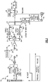
Figure 1 is a schematic diagram of a communications systems that includes a transmit device paired with a receive device according to an embodiment. -
Figure 2 is a schematic diagram of a receive device in accordance with an embodiment. -
Figure 3A is a graph of a frequency-shift keying signal with no frequency offset and a frequency response of a channelization filter of a receive device. -
Figure 3B is a graph of a frequency-shift keying signal with frequency offset and a frequency response of a channelization filter of a receive device. -
Figure 4 is waveform of a frequency shift-keying signal in accordance with an embodiment. -
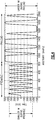
Figure 5 shows spectral plots for different modulation index values. -
Figure 6 is a schematic diagram of a transmit signal chain according to an embodiment. -
Figure 7 is a schematic diagram of a transceiver integrated circuit according to an embodiment. - The following detailed description of certain embodiments presents various descriptions of specific embodiments. However, the innovations described herein can be embodied in a multitude of different ways, for example, as defined and covered by the claims. In this description, reference is made to the drawings where like reference numerals can indicate identical or functionally similar elements. It will be understood that elements illustrated in the figures are not necessarily drawn to scale. Moreover, it will be understood that certain embodiments can include more elements than illustrated in a drawing and/or a subset of the elements illustrated in a drawing. Further, some embodiments can incorporate any suitable combination of features from two or more drawings. The headings provided herein are for convenience only and do not necessarily affect the scope or meaning of the claims.
- In Gaussian frequency-shift keying (GFSK) systems, frequency correction can be performed in a receive device during processing of a preamble of a packet. When there is a relatively large frequency error, the preamble of the packet can be filtered by a receiver such that frequency measurement accuracy can be compromised. Aspects of this disclosure relate to changing a protocol so that a modulation index (MI) has a smaller magnitude for the preamble of a packet relative to other parts of the packet, such as a payload of the packet. This adjustment of the modulation index can ensure that an entire signal is within a passband of a channelization filter of the receiver of a receive device. Accordingly, frequency adjustment in the receiver can be performed on an accurately measured frequency.
- A transmit device can adjust a modulation index of a frequency-shift keying (FSK) signal such that a preamble of a packet has a modulation index with a smaller magnitude than a modulation index for an other portion of the packet. The other portion of the packet can be the remainder of the packet. The modulation index represents an amount by which a modulated variable varies around an unmodulated level. With a modulation index having a smaller magnitude for the preamble, more of the FSK signal received by a receive device can be within a passband of a channelization filter of the receive device in the presence of a relatively large frequency offset. Frequency correction can be performed during processing of the preamble. After frequency correction is performed, the remainder of the packet having a relatively larger magnitude modulation index can be processed by the receiver. As such, after frequency correction has been completed and the receiver is processing the other portion (e.g., the remainder) of the packet, the modulation index can have an intended value for a particular application.
- Accordingly, a communications protocol can involve adjusting modulation index such that modulation index is reduced for a preamble relative to the remainder of the packet, for example, the payload. This can have the impact of reducing the frequency deviation of the preamble to the point where the FSK signal can reside entirely in-band in a channelization filter in a receiver even in the presence of a relatively large frequency offset.
- Modulation index adjustment discussed herein can improve robustness of a communications system, such as improving robustness of calibration of a receive device. With the modulation index adjustment discussed herein, a modulation index of a preamble of a packet can be independent of information being transmitted by the packet. For instance, the modulation index of the preamble can have a value that does not encode any information being transmitted by the packet. Accordingly, a receive device that receives the packet can process the packet without any modulation index information in certain applications. This can enable a transmit device in accordance with the principles and advantages discussed herein to communication with a variety of receive devices. All control information of the packet can be included outside of the preamble. For example, data rate information can be included in the packet outside of the preamble. A modulation index of the remainder of the packet can also be of information being transmitted by the packet.
- The modulation index of the preamble can have a smaller magnitude than the modulation index of an other portion of the packet, which can be some or all of the remainder of the packet. The other portion of the packet can be a payload or a payload together with one or more additional fields. The modulation index for the preamble of a packet can have the same sign as the modulation index for the other portion of the packet (i.e., both modulation indexes can be positive or both modulation indexes can be negative). A first modulation index of the preamble can have a magnitude that is within approximately 50% of a magnitude of a second modulation index of a payload. In some of instances, the first modulation index of the preamble can have a magnitude that is within approximately 25% of a magnitude of a second modulation index of a payload. For example, in certain instances, the second modulation index can be 0.5 and the first modulation index can be 0.4. As another example, the second modulation index can be 0.5 and the first modulation index can be 0.3 in certain applications. The first modulation index of the preamble can have a substantially constant value throughout substantially all of the preamble. The second modulation index of the other portion of the packet can have a substantially constant value throughout substantially the other portion of the packet.
- Advantages of the communications protocol discussed herein can include one or more of the following advantages, among other. The channelization filter of the receiver can avoid filtering an in-band signal during an automatic frequency control (AFC) measurement. This can be achieved without reducing blocker selectivity. Other preamble related activities, such as signal-detect and automatic gain control (AGC), can be unaffected. Such other preamble related activities can be unaffected by frequency measurements and can be based on other measurements, such as power measurements. Fixed-point restrictions on the output of an arctangent (ATAN) block that adjusts I and Q signals to frequency can be alleviated. For example, for relatively extreme frequency offsets, there is a possibility that the ATAN block can introduce digital wraparounds, which would compromise the AFC measurement accuracy. The receiver may not need to be tuned differently if the MI value changes. In some instances, the receiver can be function properly without any changes related to adjusting the MI during the preamble. The receiver can be backwards compatible to existing technology. Modifications to the transmitter on the pairing device can be relatively straightforward.
-
Figure 1 is a schematic diagram of acommunications systems 10 that includes a transmitdevice 20 paired with a receivedevice 30 according to an embodiment. The transmitdevice 20 can wirelessly transmit an FSK signal to the receivedevice 30. The receivedevice 30 can process the FSK signal. The transmitdevice 20 and the receivedevice 30 are both communications devices. In some instances, the transmitdevice 20 can include additional circuitry (not illustrated inFigure 1 ) to perform receive functionality in accordance with any suitable principles and advantages discussed herein. Similarly, in some instances, the receivedevice 30 can include additional circuitry (not illustrated inFigure 1 ) to perform transmit features in accordance with any suitable principles and advantages discussed herein. - In the
communications system 10, the transmitdevice 20 can generate an FSK signal that includes a packet commencing with a preamble . FSK includes a variety of frequency modulation protocols including, for example, GFSK, continuous phase frequency-shift keying (CPFSK), and minimum frequency-shift keying (MSK). The FSK signal has a modulation index. The modulation index represents an amount by which a modulated variable varies around an unmodulated level. In an FSK signal, the modulation index can represent a peak frequency deviation divided by a highest frequency component of a modulating signal, for example. - The transmit
device 20 can control the modulation index of the FSK signal. For instance, a multiplier controlled by a state machine can give a different modulation index for a preamble of a packet versus for a remainder of the packet. The receivedevice 30 can receive the FSK signal and demodulate it to an instantaneous frequency signal. For certain modes of operation (e.g., hunt mode in the illustrated diagram), the receivedevice 30 can be provided with modulation index information during the preamble to assist with operation of the initial sub-systems, such as AFC. For a number of other modes of operation, the receiver can operate autonomously to the modulation index of the FSK signal. - The transmit
device 20 can control the modulation index of the packet so that the modulation index has a smaller magnitude for the preamble than for the remainder of the packet. As illustrated, the transmitdevice 20 includes aGaussian filter 21, amultiplier 22, afinite state machine 23, a phase-locked loop (PLL) 24, apower amplifier 25, anintegrated circuit contact 26, and anantenna 27. - A digital input signal that that includes a bit stream can be modulated by a modulation circuit. The modulation circuit can operate in a digital domain. In such instances, the modulation circuit can be referred to as a digital modulation circuit. The modulation circuit of illustrated transmit
device 20 includes theGaussian filter 21, themultiplier 22, and thefinite state machine 23. TheGaussian filter 21 can filter pulses of the bit stream to make transitions smoother. Themultiplier 22 can multiply the output of theGaussian filter 21 by a modulation index adjust signal MI Adjust provided by thefinite state machine 23. Themultiplier 22 can be any circuit that can perform a suitable multiplication operation. Themultiplier 22 can be implemented by digital circuits in certain applications. Thefinite state machine 23 can control the modulation index adjust signal MI Adjust so that an FSK signal generated by the transmitter has a smaller magnitude modulation index for a preamble of a packet than for the rest of the packet. The rest of the packet can include an access address field and a payload as illustrated. In some other instances, the rest of the packet can include one or more additional fields and/or a subset of the illustrated fields. - A frequency synthesizer can receive an output of the modulation circuit and output an FSK signal that includes a packet, which contains a preamble for the earlier portion of the packet. The modulation circuit adjusting modulation can cause the preamble to have a first modulation index and a payload of the packet to have a second modulation index, in which the first second modulation index has a greater magnitude than the first modulation index. In the illustrated transmit
device 20, the frequency synthesizer is thePLL 24. ThePLL 24 receives an output of the modulation circuit, which can adjust phase and/or frequency of an output of the PLL. As illustrated, thePLL 24 can also receive an amplitude signal that controls an amplitude of the output of thePLL 24. - The FSK signal from the
PLL 24 can be amplified by thepower amplifier 25. The illustratedpower amplifier 25 has an output connected to the integratedcircuit contact 26. Theintegrated circuit contact 26 is connected to anantenna 27, which is implemented external to an integrated circuit that includes the modulation circuit,PLL 24, andpower amplifier 25 in the illustrated transmitdevice 20. Theantenna 27 transmits the FSK signal to the receivedevice 30. - As illustrated, the receive
device 30 includes anantenna 31, anintegrated circuit contact 32, a radio frequency front end (RF FE) 33,mixers local oscillator 35, IQquadrature generation circuit 36, analog-to-digital converters (ADCs) 37A and 37B,channelization filters 38A and 38B,switches ATAN block 40, a firstpacket detection circuit 43, and secondpacket detection circuit 44,switch 45,AFC circuit 46,summer 47,timing synchronization circuit 48,switch 49, andbit recovery circuit 50. - The
antenna 31 can receive the FSK signal from the transmitdevice 20. Theantenna 31 is implemented external to an integrated circuit that includes the other illustrated circuitry of the receiver. Theantenna 31 is connected to theRF FE 33 by way of the integratedcircuit contact 32. TheRF FE 33 can process the FSK signal. For instance, theRF FE 33 can include a low noise amplifier and one or more filters. - An output of the
RF FE 33 can be down converted bymixers quadrature generation circuit 36 can receive an output of thelocal oscillator 35 and provide signals to themixers mixers ADCs 37A and 37B, respectively. Channelization filters 38A and 37B can filter the outputs ofADCs 37A and 37B, respectively.Switches channelization filters 38A and 38B, respectively, to theATAN block 40. TheATAN block 40 can perform an ATAN function. TheATAN block 40 can convert processed I and Q signals to a frequency. Any suitable circuit that convert I and Q signals to a frequency can be implemented in place of theATAN block 40. - A packet can be detected by a first
packet detection circuit 43 and/or a secondpacket detection circuit 44. The firstpacket detection circuit 43 can use modulation index information to identify the packet. For example, the first packet detection circuit can be a hunt mode packet detection circuit. In hunt mode, packet detection can involve using modulation index information. The secondpacket detection circuit 44 can detect a packet without using modulation index information. The secondpacket detection circuit 44 can detect a packet in modes other than hunt mode, such as during typical operation. Aswitch 45 can selectively electrically connect the firstpacket detection circuit 43 or the secondpacket detection circuit 44 to theAFC circuit 46 based on a mode of operation of the receiver. - The
AFC circuit 46 can detect a frequency based on an instantaneous frequency contained in the preamble. TheAFC circuit 46 can include a state machine. TheAFC circuit 46 can generate frequency correction information Frecovery. Thesummer 47 can adjust an output of theATAN block 40 by the frequency correction information Frecovery to correct for a frequency offset in the FSK signal received by the receivedevice 30. For instance, thesummer 47 can subtract a frequency correction value from the output of theATAN block 40. Thesummer 47 is an example of a correction circuit that can perform any suitable frequency correction operation, such as addition, subtract, the like, or any suitable combination thereof. The frequency correction information Frecovery can be determined while a preamble is being processed. The frequency correction information Frecovery can be set for the duration of the remainder of the packet. - A frequency corrected signal provided by the
summer 47 can be further processed. Atiming synchronization circuit 78 can control aswitch 49 that provides the frequency corrected signal to abit recovery circuit 50 that generates bits corresponding to the FSK signal received from the transmitdevice 20. - Accordingly, in the
communications system 10, the transmitdevice 20 can transmit a packet using frequency-shift keying. The transmitdevice 20 can generate a preamble of the packet such that the preamble has a first modulation index, in which the packet is modulated with frequency-shift keying. The transmitdevice 20 can generate the remaining portion of the packet containing a second modulation index, in which the second modulation index has a greater magnitude than the first modulation index. The transmitdevice 20 can transmit the packet to the receivedevice 30. The receivedevice 30 can process the packet. A receive signal path of the receivedevice 30 can perform frequency correction based on an output of a channelization filter, in which the output is associated with the preamble. Then the receive signal path can demodulate the remainder of the packet, which has a modulation index with a greater magnitude than the modulation index of the preamble. -
Figure 2 is a schematic diagram of a receivedevice 60 according to an embodiment. The receivedevice 60 is similar to the receivedevice 30 ofFigure 1 . Any suitable principles and advantages of these receive devices can be implemented in accordance with the modulation index adjustment disclosed herein. In thereceiver 60, anRF FE 63 can down convert an FSK signal received by anantenna 31 to baseband. Abaseband filter 65 can filter an output of theRF FE 63. TheADC 37 can convert the output of thebaseband filter 65 to a digital signal. Thechannelization filter 38 can filter an output of theADC 37. The output of thechannelization filter 38 is connected to theATAN block 40. While only one signal path from theRF FE 63 to theATAN block 40 is shown inFigure 2 , an I path and a Q path can be included between theRF FE 63 and theATAN block 40. - The receive
device 60 includes a receiver with automatic frequency correction (AFC). In this receiver, frequency error can manifest itself as a direct current (DC) offset at the output of theATAN block 40. Frequency error can be measured during preamble where the frequency pattern is deterministic. TheAFC circuit 46 can measure the frequency error. For a specified period (e.g., a few symbols), the average frequency can be measured. A single-shot adjustment can then be made. TheAFC circuit 46 can output an AFC offset adjustment value. Thesummer 47 can adjust the output of theATAN block 40 by the AFC offset adjustment value to reduce and/or eliminate the frequency error. Thesummer 47 can add and/or subtract an output of theAFC circuit 46 to/from the output of the ATAN block. The AFC offset adjustment value can be constant while the rest of the packet other than the preamble is being processed. The output of thesummer 47 can then be demodulated into bits. - The
channelization filter 38 can offer a relatively tight selectivity around a wanted channel bandwidth. However, if a large frequency error exists, then the preamble, from which the AFC offset adjustment value is derived, can be significantly filtered. In certain cases, this can lead to a relatively poor AFC detection and correction. Consequently, throughput can be degraded. -
Figure 3A is a graph of a frequency-shift keying signal with no frequency offset and a frequency response of thechannelization filter 38 of the receivedevice 60. In contrast,Figure 3B is a graph of a frequency-shift keying signal with frequency offset and the frequency response of thechannelization filter 38. These figures illustrate the frequency of a preamble versus time with no frequency offset and with a frequency offset that can result in part of the preamble being filtered by thechannelization filter 38. When part of the preamble is filtered out, data can be corrupted. - The modulation in the transmit
device 20 discussed with reference toFigure 1 can reduce the frequency deviation of the preamble such that the FSK signal can be entirely in-band. Accordingly, the preamble can be within the passband of thechannelization filter 38 ofFigure 2 even in the presence of a relatively large frequency offset. This can result in accurate frequency correction even in the presence of a relatively large frequency offset. The receive device can tolerate a larger frequency error with the modulation index adjustment discussed herein while maintaining desired characteristics of thechannelization filter 38. For instance, thechannelization filter 38 can have a passband corresponding to a modulation index of a non-preamble portion of a packet. Accordingly, the parameters of thechannelization filter 38 can be designed and/or optimized for processing the non-preamble portion of the packet. -
Figure 4 is waveform of a frequency shift-keying signal in accordance with an embodiment. The waveform ofFigure 4 corresponds to a signal transmitted by the transmitdevice 20 ofFigure 1 and received by the receivedevice 30 ofFigure 1 or the receivedevice 60 ofFigure 2 . This waveform shows that the FSK signal has a smaller magnitude modulation index for a preamble and a larger magnitude modulation index for the remainder of the packet. A receive device can measure frequency error (e.g., frequency offset) and make a one-shot adjustment while processing the preamble. -
Figure 5 shows spectral plots for different modulation index values. This figure shows that for a smaller magnitude of a modulation index, less bandwidth is used. For instance, less bandwidth is used when the modulation index is 0.3 compared to when the modulation index is 0.5. Accordingly, reducing the magnitude of the modulation index of a preamble will reduce bandwidth of a signal being filtered by a channelization filter of a receive device. The modulation index of 0.3 can be for a preamble of a packet and the modulation index of 0.5 can be for the remainder of the packet (including the payload) in accordance with the principles and advantages discussed herein. -
Figure 6 is a schematic diagram of a transmitsignal chain 70 according to an embodiment. In the transmitsignal chain 70, the transmitter takes on the form of a frequency synthesizer with digital control ports allowing instantaneous frequency modulation. Frequency control words can be received from a digital baseband processor. Carrier frequency adjustment and modulation are performed via the frequency synthesizer. Output signal generation and power control can be performed via the power amplifier. - The transmit
signal chain 70 includes adigital GFSK modulator 71, aPLL 72, and a power amplifier. ThePLL 72 is a frequency synthesizer. ThePLL 72 includes a voltage-controller oscillator 73, adivider 74, afeedback divider 75, and a phase frequency detector/charge pump/loop filter circuit 76. - Carrier frequency adjustment and low frequency modulation can be accomplished using a first control word TX_FM1. A
sigma delta modulator 77 can generate the first control word TX_FM1 based on an output of theGFSK modulator 71. The first control word TX_FM1 can dynamically adjust a division ratio in a feedback loop of thePLL 72. In particular, the first control word TX_FM1 can adjust a division ratio of thefeedback divider 75. The transfer function of the frequency modulation at this injection point can take on a low-pass form, with the bandwidth being defined by the PLL's loop bandwidth. - A digital-to-analog converter (DAC), such as a frequency modulated (FM)
DAC 78, can modulate the PLL's carrier frequency via a second control word TX_FM2 to provide for high frequency modulation. TheFM DAC 78 can convert the second control word TX_FM2 to an analog signal and apply the analog signal to the voltage-controlledoscillator 73 of thePLL 72. The transfer function of this injection point can take on a highpass form, with the cut-off determined by the PLL's loop bandwidth. - The
GFSK modulator 71 can scale the first control word TX_FM1 and/or the first control word TX_FM2 to adjust modulation index in accordance with the principles and advantages discussed herein. Amultiplier 22 of theGFSK modulation 71 can be used in the scaling. As illustrated, theGFSK modulator 71 can include aGaussian filter 21, themultiplier 22, and afinite state machine 23 arranged to control themultiplier 22 to cause modulation index to be adjusted in accordance with any suitable principles and advantages discussed herein. - The
power amplifier 25 can include multiple segments, each converting the PLL's output voltage waveform to a current. The output power of thepower amplifier 25 can be set by adjusting the number of active power amplifier segments. An output matching circuit (not illustrated) can be coupled between an output of the power amplifier and an antenna. -
Figure 7 is a schematic diagram of a transceiver integratedcircuit 80 according to an embodiment. Any of the transmit devices and/or the receive devices discussed herein can be implemented on a transceiver integrated circuit. As illustrated, the transceiver integratedcircuit 80 includes adigital baseband processor 81, asynthesizer 82, acrystal oscillator 83, a transmitter 84, apower amplifier 25, a receiver 85, and alow noise amplifier 86. - An analog RF FE can include the transmitter 84, the receiver 85, and the
synthesizer 82. Thetransceiver 80 can operate in a half-duplex fashion so that thesynthesizer 82 can serve the dual purpose of generating local oscillator signals for both the receiver 85 and the transmitter 84. In the transceiver integratedcircuit 80, a receive chain can include thelow noise amplifier 86, a receiver 85 that includes a heterodyne down-converter and filtering, and a data conversion stage in thebaseband processor 81. In the transceiver integratedcircuit 80, a transmitter chain can include a receiver 85 that includes a frequency agile synthesizer and thepower amplifier 25. The illustratedcrystal oscillator 83 is connected to an off-chip crystal. The radio channel frequency and symbol rate can be derived from an output of thecrystal oscillator 83. - The
digital baseband processor 81 can perform any suitable processing associated with generating signals for the transmitter 84 and/or processing signals provided by the receiver 85. Thedigital baseband processor 81 can provide digital modulation data to the transmitter 84. Thedigital baseband processor 81 can include any of the modulation circuits discussed herein, such as thedigital GFSK modulator 71 ofFigure 6 or the modulation circuit of the transmitdevice 20 ofFigure 1 . Thedigital baseband processor 81 can process baseband data from the receiver 85 to perform a variety of different processing, such as automatic gain control, synchronization, and data demodulation. Thedigital baseband processor 81 can dynamically provide configuration and/or control data to/from an RF FE that includes the transmitter 84 and the receiver 85. Thedigital baseband processor 81 can control system timing in the transceiver integratedcircuit 80. - Any of the principles and advantages discussed herein can be applied to other systems, devices, integrated circuits, electronic apparatus, not just to the embodiments described above. The elements and operations of the various embodiments described above can be combined to provide further embodiments. The principles and advantages of the embodiments can be used in connection with any other systems, devices, integrated circuits, apparatus, or methods that could benefit from any of the teachings herein.
- Aspects of this disclosure can be implemented in various electronic devices. Examples of the electronic devices can include, but are not limited to, consumer electronic products, parts of electronic products such as integrated circuits, electronic test equipment, wireless communication devices, personal area network communication devices, cellular communications infrastructure such as a base station, vehicular electronics such as automotive electronics, etc. Further, the electronic devices can include unfinished products.
- Unless the context indicates otherwise, throughout the description and the claims, the words "comprise," "comprising," "include," "including," and the like are to generally be construed in an inclusive sense, as opposed to an exclusive or exhaustive sense; that is to say, in the sense of "including, but not limited to." The word "coupled," as generally used herein, refers to two or more elements that may be either directly coupled to each other, or coupled by way of one or more intermediate elements. Likewise, the word "connected," as generally used herein, refers to two or more elements that may be either directly connected, or connected by way of one or more intermediate elements. Additionally, the words "herein," "above," "below," and words of similar import, when used in this application, shall refer to this application as a whole and not to any particular portions of this application. Where the context permits, words in the above Detailed Description using the singular or plural may also include the plural or singular, respectively. The word "or" in reference to a list of two or more items, is generally intended to encompass all of the following interpretations of the word: any of the items in the list, all of the items in the list, and any combination of the items in the list.
- Moreover, conditional language used herein, such as, among others, "can," "could," "might," "may," "e.g.," "for example," "such as" and the like, unless specifically stated otherwise or otherwise understood within the context as used, is generally intended to convey that certain embodiments include, while other embodiments do not include, certain features, elements and/or states. Thus, such conditional language is not generally intended to imply that features, elements and/or states are in any way required for one or more embodiments or that one or more embodiments necessarily include logic for deciding whether these features, elements and/or states are included or are to be performed in any particular embodiment.
- While certain embodiments have been described, these embodiments have been presented by way of example only, and are not intended to limit the scope of the disclosure. Indeed, the novel methods, apparatus, systems, devices, and integrate circuits described herein may be embodied in a variety of other forms; furthermore, various omissions, substitutions and changes in the form of the methods, apparatus, and systems described herein may be made without departing from the spirit of the disclosure. For example, circuit blocks described herein may be deleted, moved, added, subdivided, combined, and/or modified. Each of these circuit blocks may be implemented in a variety of different ways. The accompanying claims and their equivalents are intended to cover any such forms or modifications as would fall within the scope and spirit of the disclosure.
Claims (15)
- A communication device with frequency-shift keying, the communication device comprising:a modulation circuit configured to modulate a digital input signal; anda frequency synthesizer configured to receive an output of the modulation circuit and to output a frequency-shift keying signal comprising a packet, wherein the packet comprises a preamble and an other portion;wherein the modulation circuit is configured to adjust modulation to cause the preamble to have a first modulation index and the other portion to have a second modulation index, and wherein the second modulation index has a greater magnitude than the first modulation index.
- The communication device of Claim 1, wherein the modulation circuit comprises a multiplier configured to adjust modulation of the digital input signal.
- The communication device of Claim 2, further comprising a finite state machine configured to control the multiplier.
- The communication device of any preceding Claim, wherein the first modulation index and the second modulation index have the same sign.
- The communication device of any preceding Claim, wherein the first modulation index is independent of information being transmitted by the packet.
- The communication device of any preceding Claim, wherein the frequency synthesizer comprises a phase-locked loop comprising a divider, and wherein the divider is configured to receive the output of the modulation circuit.
- The communication device of Claim 6, further comprising a sigma delta modulator coupled between the modulation circuit and the divider.
- The communication device of any preceding Claim, wherein the frequency synthesizer comprises a phase locked loop comprising a controllable oscillator, wherein the controllable oscillator is configured to receive the output of the modulation circuit; and optionally further comprising a digital-to-analog converter coupled between the modulation circuit and the controllable oscillator, wherein the controllable oscillator comprises a voltage-controlled oscillator.
- The communication device of any preceding Claim, further comprising:a power amplifier configured to amplify the frequency-shift keying signal; and/ora receiver that comprises a frequency correction circuit configured to perform frequency correction based on a preamble of a received packet received by the communication device.
- A method of transmitting a packet using frequency-shift keying, the method comprising:generating a preamble of a packet such that the preamble has a first modulation index, wherein the packet is modulated with frequency-shift keying;generating a payload of the packet such that the payload has a second modulation index, wherein the second modulation index has a greater magnitude than the first modulation index; andtransmitting the packet.
- The method of Claim 10, further comprising adjusting modulation index for the packet, using a multiplier, from the first modulation index to the second modulation index.
- The method of Claims 10 or 11, wherein the first modulation index and the second modulation index are both independent of the information being transmitted by the packet; and/or the packet is modulated with Gaussian frequency-shift keying.
- A method of processing a frequency-shift keying signal, the method comprising:receiving, by a receive signal path, a frequency-shift keying signal comprising a packet that comprises a preamble and a payload, wherein the preamble has a first modulation index that has a smaller magnitude than a second modulation index of the payload;performing frequency correction based on an output of a channelization filter associated with the preamble that has the first modulation index, wherein the channelization filter is in the receive signal path; andsubsequent to said performing frequency correction, demodulating the payload that has the second modulation index.
- The method of Claim 13, further comprising measuring frequency error based on an output of a circuit that has an input coupled to the output of the channelization filter, and wherein said performing frequency correction is based on said measuring frequency error.
- The method of Claims 13 or 14, wherein one or more of the following apply:the channelization filter has a passband associated with the second modulation index;modulation index information is used in said performing frequency correction; andthe first modulation index is independent of information being transmitted by the packet.
Applications Claiming Priority (1)
| Application Number | Priority Date | Filing Date | Title |
|---|---|---|---|
| US15/716,197 US10541721B2 (en) | 2017-09-26 | 2017-09-26 | Modulation index adjustment |
Publications (2)
| Publication Number | Publication Date |
|---|---|
| EP3461092A1 true EP3461092A1 (en) | 2019-03-27 |
| EP3461092B1 EP3461092B1 (en) | 2021-05-05 |
Family
ID=63682986
Family Applications (1)
| Application Number | Title | Priority Date | Filing Date |
|---|---|---|---|
| EP18196109.5A Active EP3461092B1 (en) | 2017-09-26 | 2018-09-21 | Modulation index adjustment |
Country Status (3)
| Country | Link |
|---|---|
| US (1) | US10541721B2 (en) |
| EP (1) | EP3461092B1 (en) |
| CN (1) | CN109586741B (en) |
Cited By (1)
| Publication number | Priority date | Publication date | Assignee | Title |
|---|---|---|---|---|
| RU2822223C1 (en) * | 2023-10-03 | 2024-07-03 | Федеральное государственное бюджетное образовательное учреждение высшего образования "Московский автомобильно-дорожный государственный технический университет (МАДИ)" | Method of modulating high-frequency signals |
Families Citing this family (11)
| Publication number | Priority date | Publication date | Assignee | Title |
|---|---|---|---|---|
| CN111212006B (en) * | 2019-12-25 | 2022-07-15 | 奉加微电子(上海)有限公司 | A kind of signal demodulation system and demodulation method |
| US11240078B1 (en) * | 2020-04-21 | 2022-02-01 | Hrl Laboratories, Llc | Frequency shift keying modulator, transmitter and link |
| CN112235220B (en) * | 2020-09-25 | 2022-11-11 | 展讯通信(天津)有限公司 | Modulation index adjusting method and device and terminal equipment |
| US11088784B1 (en) | 2020-12-24 | 2021-08-10 | Aira Technologies, Inc. | Systems and methods for utilizing dynamic codes with neural networks |
| US11575469B2 (en) | 2020-12-28 | 2023-02-07 | Aira Technologies, Inc. | Multi-bit feedback protocol systems and methods |
| US11368251B1 (en) | 2020-12-28 | 2022-06-21 | Aira Technologies, Inc. | Convergent multi-bit feedback system |
| US11483109B2 (en) | 2020-12-28 | 2022-10-25 | Aira Technologies, Inc. | Systems and methods for multi-device communication |
| CN112804174B (en) * | 2020-12-30 | 2023-03-24 | 湖南艾科诺维科技有限公司 | GFSK digital modulation device with variable code rate and modulation index |
| US12199759B2 (en) | 2021-03-09 | 2025-01-14 | Intel Corporation | Asynchronous input dependency resolution mechanism |
| US11489623B2 (en) | 2021-03-15 | 2022-11-01 | Aira Technologies, Inc. | Error correction in network packets |
| US11496242B2 (en) | 2021-03-15 | 2022-11-08 | Aira Technologies, Inc. | Fast cyclic redundancy check: utilizing linearity of cyclic redundancy check for accelerating correction of corrupted network packets |
Citations (2)
| Publication number | Priority date | Publication date | Assignee | Title |
|---|---|---|---|---|
| EP0377180A2 (en) * | 1989-01-03 | 1990-07-11 | Motorola, Inc. | All-digital quadrature modulator |
| US20160373279A1 (en) * | 2015-02-04 | 2016-12-22 | Telefonaktiebolaget Lm Ericsson (Publ) | Modulation Index Shift Signaling |
Family Cites Families (17)
| Publication number | Priority date | Publication date | Assignee | Title |
|---|---|---|---|---|
| US5272446A (en) * | 1991-11-29 | 1993-12-21 | Comsat | Digitally implemented fast frequency estimator/demodulator for low bit rate maritime and mobile data communications without the use of an acquisition preamble |
| US5832022A (en) | 1995-06-02 | 1998-11-03 | Omnipoint Corporation | Method and apparatus for controlling the modulation index of continuous phase modulated (CPM) signals |
| US6008703A (en) * | 1997-01-31 | 1999-12-28 | Massachusetts Institute Of Technology | Digital compensation for wideband modulation of a phase locked loop frequency synthesizer |
| JP2000307666A (en) * | 1999-04-26 | 2000-11-02 | Kenwood Corp | Frequency shift modulating circuit |
| US7385929B1 (en) * | 2001-09-25 | 2008-06-10 | Atheros Communications, Inc. | Method and system for detecting false packets in wireless communications systems |
| US6694742B2 (en) * | 2002-06-26 | 2004-02-24 | General Electric Company | Gas turbine system operation based on estimated stress |
| US20040001447A1 (en) | 2002-06-28 | 2004-01-01 | Schafer David C. | Wireless communication airlink protocol |
| US20040001448A1 (en) | 2002-06-28 | 2004-01-01 | Preston Shawn E. | System and method for transmitting highly correlated preambles in QAM constellations |
| WO2004021659A1 (en) * | 2002-08-28 | 2004-03-11 | Philips Intellectual Property & Standards Gmbh | Method for generating i/q signal in a tdma transmitter and corresponding modulator |
| JP3858021B2 (en) * | 2003-12-26 | 2006-12-13 | 松下電器産業株式会社 | Modulator, semiconductor integrated circuit, wired and wireless communication device |
| US7421006B2 (en) | 2004-03-16 | 2008-09-02 | Harris Corporation | System and method for coherent multi-h continuous phase modulation waveform |
| TWI278184B (en) * | 2005-05-23 | 2007-04-01 | Novatek Microelectronics Corp | A modulation method and apparatus with adjustable divisors of the dividers in phase-locked loop |
| US8761230B2 (en) * | 2009-06-08 | 2014-06-24 | Adeptence, Llc | Method and apparatus for continuous phase modulation preamble encoding and decoding |
| US8401118B2 (en) * | 2009-06-09 | 2013-03-19 | Adeptence Llc | Method and apparatus for constant envelope demodulation |
| CN102769462A (en) * | 2011-05-06 | 2012-11-07 | 成都天奥电子股份有限公司 | Direct digital frequency phase-locked frequency multiplier circuit |
| US8497716B2 (en) * | 2011-08-05 | 2013-07-30 | Qualcomm Incorporated | Phase locked loop with phase correction in the feedback loop |
| US9712356B2 (en) | 2015-04-14 | 2017-07-18 | Texas Instruments Incorporated | Managing multiple modulation schemes with coded modulation indicator in default-modulated preamble |
-
2017
- 2017-09-26 US US15/716,197 patent/US10541721B2/en active Active
-
2018
- 2018-09-21 EP EP18196109.5A patent/EP3461092B1/en active Active
- 2018-09-26 CN CN201811120116.3A patent/CN109586741B/en active Active
Patent Citations (2)
| Publication number | Priority date | Publication date | Assignee | Title |
|---|---|---|---|---|
| EP0377180A2 (en) * | 1989-01-03 | 1990-07-11 | Motorola, Inc. | All-digital quadrature modulator |
| US20160373279A1 (en) * | 2015-02-04 | 2016-12-22 | Telefonaktiebolaget Lm Ericsson (Publ) | Modulation Index Shift Signaling |
Cited By (1)
| Publication number | Priority date | Publication date | Assignee | Title |
|---|---|---|---|---|
| RU2822223C1 (en) * | 2023-10-03 | 2024-07-03 | Федеральное государственное бюджетное образовательное учреждение высшего образования "Московский автомобильно-дорожный государственный технический университет (МАДИ)" | Method of modulating high-frequency signals |
Also Published As
| Publication number | Publication date |
|---|---|
| US20190097680A1 (en) | 2019-03-28 |
| US10541721B2 (en) | 2020-01-21 |
| EP3461092B1 (en) | 2021-05-05 |
| CN109586741A (en) | 2019-04-05 |
| CN109586741B (en) | 2021-03-09 |
Similar Documents
| Publication | Publication Date | Title |
|---|---|---|
| EP3461092B1 (en) | Modulation index adjustment | |
| US10742462B2 (en) | BPSK demodulation | |
| EP1710967B1 (en) | Method and system for using PSK SYNC word for fine frequency adjustment | |
| EP0835557B1 (en) | Digitally compensated direct conversion receiver | |
| TWI597957B (en) | Low-power, noise insensitive communication channel system and related method using logarithmic detector amplifier (lda) demodulator | |
| JP3744546B2 (en) | Variable of sampled signal C. Method and apparatus for compensating offset | |
| EP2905905B1 (en) | System for direct conversion receivers | |
| EP0594894A1 (en) | DC offset correction for direct-conversion TDMA receiver | |
| EP1653616B1 (en) | A method and system for frequency feedback adjustment in digital receivers | |
| US10484215B2 (en) | Asynchronous transmission for NFC card emulation mode | |
| US8324962B2 (en) | Apparatus and method for demodulation | |
| CN108337203B (en) | Clock correction method and Bluetooth chip | |
| CN108306628B (en) | Amplitude demodulator and method of demodulating an input signal | |
| EP3182584B1 (en) | Phase tracking receiver | |
| US7542527B2 (en) | Frequency offset correction circuit device | |
| JP4316198B2 (en) | Semiconductor device, receiver, and control method of semiconductor device | |
| US20060115021A1 (en) | Compensation for the carrier frequency offset in a receiving apparatus, which is designed for a plurality of modulation types, in a mobile communications system | |
| US10841217B2 (en) | Multi-packet protocol header detection | |
| CN103840848A (en) | Adaptive dc offset cancellation for direct conversion rf receivers | |
| US7573948B2 (en) | Radio transmitter incorporating digital modulator and circuitry to accommodate baseband processor with analog interface | |
| US20160226686A1 (en) | Receiving apparatus and receiving method | |
| US6567479B1 (en) | System and method for extracting and compensating for reference frequency error in a communications system | |
| US9071417B2 (en) | Method and system for packet synchronization | |
| JP3898839B2 (en) | Transmitter | |
| US11569854B1 (en) | RF receiver and method for simultaneously compensating carrier frequency offset and optimizing bandwidth by using preamble of a received RF signal |
Legal Events
| Date | Code | Title | Description |
|---|---|---|---|
| PUAI | Public reference made under article 153(3) epc to a published international application that has entered the european phase |
Free format text: ORIGINAL CODE: 0009012 |
|
| STAA | Information on the status of an ep patent application or granted ep patent |
Free format text: STATUS: THE APPLICATION HAS BEEN PUBLISHED |
|
| AK | Designated contracting states |
Kind code of ref document: A1 Designated state(s): AL AT BE BG CH CY CZ DE DK EE ES FI FR GB GR HR HU IE IS IT LI LT LU LV MC MK MT NL NO PL PT RO RS SE SI SK SM TR |
|
| AX | Request for extension of the european patent |
Extension state: BA ME |
|
| STAA | Information on the status of an ep patent application or granted ep patent |
Free format text: STATUS: REQUEST FOR EXAMINATION WAS MADE |
|
| 17P | Request for examination filed |
Effective date: 20190603 |
|
| RBV | Designated contracting states (corrected) |
Designated state(s): AL AT BE BG CH CY CZ DE DK EE ES FI FR GB GR HR HU IE IS IT LI LT LU LV MC MK MT NL NO PL PT RO RS SE SI SK SM TR |
|
| GRAP | Despatch of communication of intention to grant a patent |
Free format text: ORIGINAL CODE: EPIDOSNIGR1 |
|
| STAA | Information on the status of an ep patent application or granted ep patent |
Free format text: STATUS: GRANT OF PATENT IS INTENDED |
|
| INTG | Intention to grant announced |
Effective date: 20201204 |
|
| GRAS | Grant fee paid |
Free format text: ORIGINAL CODE: EPIDOSNIGR3 |
|
| GRAA | (expected) grant |
Free format text: ORIGINAL CODE: 0009210 |
|
| STAA | Information on the status of an ep patent application or granted ep patent |
Free format text: STATUS: THE PATENT HAS BEEN GRANTED |
|
| RAP1 | Party data changed (applicant data changed or rights of an application transferred) |
Owner name: ANALOG DEVICES INTERNATIONAL UNLIMITED COMPANY |
|
| AK | Designated contracting states |
Kind code of ref document: B1 Designated state(s): AL AT BE BG CH CY CZ DE DK EE ES FI FR GB GR HR HU IE IS IT LI LT LU LV MC MK MT NL NO PL PT RO RS SE SI SK SM TR |
|
| REG | Reference to a national code |
Ref country code: GB Ref legal event code: FG4D |
|
| REG | Reference to a national code |
Ref country code: CH Ref legal event code: EP |
|
| REG | Reference to a national code |
Ref country code: AT Ref legal event code: REF Ref document number: 1391238 Country of ref document: AT Kind code of ref document: T Effective date: 20210515 |
|
| REG | Reference to a national code |
Ref country code: IE Ref legal event code: FG4D |
|
| REG | Reference to a national code |
Ref country code: DE Ref legal event code: R096 Ref document number: 602018016534 Country of ref document: DE |
|
| REG | Reference to a national code |
Ref country code: LT Ref legal event code: MG9D |
|
| REG | Reference to a national code |
Ref country code: AT Ref legal event code: MK05 Ref document number: 1391238 Country of ref document: AT Kind code of ref document: T Effective date: 20210505 |
|
| PG25 | Lapsed in a contracting state [announced via postgrant information from national office to epo] |
Ref country code: HR Free format text: LAPSE BECAUSE OF FAILURE TO SUBMIT A TRANSLATION OF THE DESCRIPTION OR TO PAY THE FEE WITHIN THE PRESCRIBED TIME-LIMIT Effective date: 20210505 Ref country code: LT Free format text: LAPSE BECAUSE OF FAILURE TO SUBMIT A TRANSLATION OF THE DESCRIPTION OR TO PAY THE FEE WITHIN THE PRESCRIBED TIME-LIMIT Effective date: 20210505 Ref country code: FI Free format text: LAPSE BECAUSE OF FAILURE TO SUBMIT A TRANSLATION OF THE DESCRIPTION OR TO PAY THE FEE WITHIN THE PRESCRIBED TIME-LIMIT Effective date: 20210505 Ref country code: AT Free format text: LAPSE BECAUSE OF FAILURE TO SUBMIT A TRANSLATION OF THE DESCRIPTION OR TO PAY THE FEE WITHIN THE PRESCRIBED TIME-LIMIT Effective date: 20210505 Ref country code: BG Free format text: LAPSE BECAUSE OF FAILURE TO SUBMIT A TRANSLATION OF THE DESCRIPTION OR TO PAY THE FEE WITHIN THE PRESCRIBED TIME-LIMIT Effective date: 20210805 |
|
| PGFP | Annual fee paid to national office [announced via postgrant information from national office to epo] |
Ref country code: IE Payment date: 20210719 Year of fee payment: 4 |
|
| PG25 | Lapsed in a contracting state [announced via postgrant information from national office to epo] |
Ref country code: SE Free format text: LAPSE BECAUSE OF FAILURE TO SUBMIT A TRANSLATION OF THE DESCRIPTION OR TO PAY THE FEE WITHIN THE PRESCRIBED TIME-LIMIT Effective date: 20210505 Ref country code: RS Free format text: LAPSE BECAUSE OF FAILURE TO SUBMIT A TRANSLATION OF THE DESCRIPTION OR TO PAY THE FEE WITHIN THE PRESCRIBED TIME-LIMIT Effective date: 20210505 Ref country code: LV Free format text: LAPSE BECAUSE OF FAILURE TO SUBMIT A TRANSLATION OF THE DESCRIPTION OR TO PAY THE FEE WITHIN THE PRESCRIBED TIME-LIMIT Effective date: 20210505 Ref country code: PL Free format text: LAPSE BECAUSE OF FAILURE TO SUBMIT A TRANSLATION OF THE DESCRIPTION OR TO PAY THE FEE WITHIN THE PRESCRIBED TIME-LIMIT Effective date: 20210505 Ref country code: PT Free format text: LAPSE BECAUSE OF FAILURE TO SUBMIT A TRANSLATION OF THE DESCRIPTION OR TO PAY THE FEE WITHIN THE PRESCRIBED TIME-LIMIT Effective date: 20210906 Ref country code: NO Free format text: LAPSE BECAUSE OF FAILURE TO SUBMIT A TRANSLATION OF THE DESCRIPTION OR TO PAY THE FEE WITHIN THE PRESCRIBED TIME-LIMIT Effective date: 20210805 Ref country code: IS Free format text: LAPSE BECAUSE OF FAILURE TO SUBMIT A TRANSLATION OF THE DESCRIPTION OR TO PAY THE FEE WITHIN THE PRESCRIBED TIME-LIMIT Effective date: 20210905 Ref country code: GR Free format text: LAPSE BECAUSE OF FAILURE TO SUBMIT A TRANSLATION OF THE DESCRIPTION OR TO PAY THE FEE WITHIN THE PRESCRIBED TIME-LIMIT Effective date: 20210806 |
|
| REG | Reference to a national code |
Ref country code: NL Ref legal event code: MP Effective date: 20210505 |
|
| PG25 | Lapsed in a contracting state [announced via postgrant information from national office to epo] |
Ref country code: NL Free format text: LAPSE BECAUSE OF FAILURE TO SUBMIT A TRANSLATION OF THE DESCRIPTION OR TO PAY THE FEE WITHIN THE PRESCRIBED TIME-LIMIT Effective date: 20210505 |
|
| PG25 | Lapsed in a contracting state [announced via postgrant information from national office to epo] |
Ref country code: ES Free format text: LAPSE BECAUSE OF FAILURE TO SUBMIT A TRANSLATION OF THE DESCRIPTION OR TO PAY THE FEE WITHIN THE PRESCRIBED TIME-LIMIT Effective date: 20210505 Ref country code: EE Free format text: LAPSE BECAUSE OF FAILURE TO SUBMIT A TRANSLATION OF THE DESCRIPTION OR TO PAY THE FEE WITHIN THE PRESCRIBED TIME-LIMIT Effective date: 20210505 Ref country code: SK Free format text: LAPSE BECAUSE OF FAILURE TO SUBMIT A TRANSLATION OF THE DESCRIPTION OR TO PAY THE FEE WITHIN THE PRESCRIBED TIME-LIMIT Effective date: 20210505 Ref country code: SM Free format text: LAPSE BECAUSE OF FAILURE TO SUBMIT A TRANSLATION OF THE DESCRIPTION OR TO PAY THE FEE WITHIN THE PRESCRIBED TIME-LIMIT Effective date: 20210505 Ref country code: DK Free format text: LAPSE BECAUSE OF FAILURE TO SUBMIT A TRANSLATION OF THE DESCRIPTION OR TO PAY THE FEE WITHIN THE PRESCRIBED TIME-LIMIT Effective date: 20210505 Ref country code: CZ Free format text: LAPSE BECAUSE OF FAILURE TO SUBMIT A TRANSLATION OF THE DESCRIPTION OR TO PAY THE FEE WITHIN THE PRESCRIBED TIME-LIMIT Effective date: 20210505 Ref country code: RO Free format text: LAPSE BECAUSE OF FAILURE TO SUBMIT A TRANSLATION OF THE DESCRIPTION OR TO PAY THE FEE WITHIN THE PRESCRIBED TIME-LIMIT Effective date: 20210505 |
|
| REG | Reference to a national code |
Ref country code: DE Ref legal event code: R097 Ref document number: 602018016534 Country of ref document: DE |
|
| PLBE | No opposition filed within time limit |
Free format text: ORIGINAL CODE: 0009261 |
|
| STAA | Information on the status of an ep patent application or granted ep patent |
Free format text: STATUS: NO OPPOSITION FILED WITHIN TIME LIMIT |
|
| 26N | No opposition filed |
Effective date: 20220208 |
|
| REG | Reference to a national code |
Ref country code: CH Ref legal event code: PL |
|
| REG | Reference to a national code |
Ref country code: BE Ref legal event code: MM Effective date: 20210930 |
|
| PG25 | Lapsed in a contracting state [announced via postgrant information from national office to epo] |
Ref country code: IS Free format text: LAPSE BECAUSE OF FAILURE TO SUBMIT A TRANSLATION OF THE DESCRIPTION OR TO PAY THE FEE WITHIN THE PRESCRIBED TIME-LIMIT Effective date: 20210905 Ref country code: MC Free format text: LAPSE BECAUSE OF FAILURE TO SUBMIT A TRANSLATION OF THE DESCRIPTION OR TO PAY THE FEE WITHIN THE PRESCRIBED TIME-LIMIT Effective date: 20210505 Ref country code: AL Free format text: LAPSE BECAUSE OF FAILURE TO SUBMIT A TRANSLATION OF THE DESCRIPTION OR TO PAY THE FEE WITHIN THE PRESCRIBED TIME-LIMIT Effective date: 20210505 |
|
| PG25 | Lapsed in a contracting state [announced via postgrant information from national office to epo] |
Ref country code: LU Free format text: LAPSE BECAUSE OF NON-PAYMENT OF DUE FEES Effective date: 20210921 Ref country code: IT Free format text: LAPSE BECAUSE OF FAILURE TO SUBMIT A TRANSLATION OF THE DESCRIPTION OR TO PAY THE FEE WITHIN THE PRESCRIBED TIME-LIMIT Effective date: 20210505 Ref country code: FR Free format text: LAPSE BECAUSE OF NON-PAYMENT OF DUE FEES Effective date: 20210930 Ref country code: BE Free format text: LAPSE BECAUSE OF NON-PAYMENT OF DUE FEES Effective date: 20210930 |
|
| PG25 | Lapsed in a contracting state [announced via postgrant information from national office to epo] |
Ref country code: LI Free format text: LAPSE BECAUSE OF NON-PAYMENT OF DUE FEES Effective date: 20210930 Ref country code: CH Free format text: LAPSE BECAUSE OF NON-PAYMENT OF DUE FEES Effective date: 20210930 |
|
| PG25 | Lapsed in a contracting state [announced via postgrant information from national office to epo] |
Ref country code: CY Free format text: LAPSE BECAUSE OF FAILURE TO SUBMIT A TRANSLATION OF THE DESCRIPTION OR TO PAY THE FEE WITHIN THE PRESCRIBED TIME-LIMIT Effective date: 20210505 |
|
| PG25 | Lapsed in a contracting state [announced via postgrant information from national office to epo] |
Ref country code: IE Free format text: LAPSE BECAUSE OF NON-PAYMENT OF DUE FEES Effective date: 20220921 Ref country code: HU Free format text: LAPSE BECAUSE OF FAILURE TO SUBMIT A TRANSLATION OF THE DESCRIPTION OR TO PAY THE FEE WITHIN THE PRESCRIBED TIME-LIMIT; INVALID AB INITIO Effective date: 20180921 |
|
| PG25 | Lapsed in a contracting state [announced via postgrant information from national office to epo] |
Ref country code: MK Free format text: LAPSE BECAUSE OF FAILURE TO SUBMIT A TRANSLATION OF THE DESCRIPTION OR TO PAY THE FEE WITHIN THE PRESCRIBED TIME-LIMIT Effective date: 20210505 |
|
| PG25 | Lapsed in a contracting state [announced via postgrant information from national office to epo] |
Ref country code: MT Free format text: LAPSE BECAUSE OF FAILURE TO SUBMIT A TRANSLATION OF THE DESCRIPTION OR TO PAY THE FEE WITHIN THE PRESCRIBED TIME-LIMIT Effective date: 20210505 |
|
| PGFP | Annual fee paid to national office [announced via postgrant information from national office to epo] |
Ref country code: DE Payment date: 20250820 Year of fee payment: 8 |
|
| PGFP | Annual fee paid to national office [announced via postgrant information from national office to epo] |
Ref country code: GB Payment date: 20250820 Year of fee payment: 8 |
|
| PG25 | Lapsed in a contracting state [announced via postgrant information from national office to epo] |
Ref country code: TR Free format text: LAPSE BECAUSE OF FAILURE TO SUBMIT A TRANSLATION OF THE DESCRIPTION OR TO PAY THE FEE WITHIN THE PRESCRIBED TIME-LIMIT Effective date: 20210505 |