EP3460907A1 - Array antenna device - Google Patents
Array antenna device Download PDFInfo
- Publication number
- EP3460907A1 EP3460907A1 EP16905426.9A EP16905426A EP3460907A1 EP 3460907 A1 EP3460907 A1 EP 3460907A1 EP 16905426 A EP16905426 A EP 16905426A EP 3460907 A1 EP3460907 A1 EP 3460907A1
- Authority
- EP
- European Patent Office
- Prior art keywords
- patch
- line
- patch antenna
- coupling
- antenna
- Prior art date
- Legal status (The legal status is an assumption and is not a legal conclusion. Google has not performed a legal analysis and makes no representation as to the accuracy of the status listed.)
- Granted
Links
Images




Classifications
-
- H—ELECTRICITY
- H01—ELECTRIC ELEMENTS
- H01Q—ANTENNAS, i.e. RADIO AERIALS
- H01Q1/00—Details of, or arrangements associated with, antennas
- H01Q1/52—Means for reducing coupling between antennas; Means for reducing coupling between an antenna and another structure
- H01Q1/521—Means for reducing coupling between antennas; Means for reducing coupling between an antenna and another structure reducing the coupling between adjacent antennas
- H01Q1/523—Means for reducing coupling between antennas; Means for reducing coupling between an antenna and another structure reducing the coupling between adjacent antennas between antennas of an array
-
- H—ELECTRICITY
- H01—ELECTRIC ELEMENTS
- H01Q—ANTENNAS, i.e. RADIO AERIALS
- H01Q21/00—Antenna arrays or systems
- H01Q21/0006—Particular feeding systems
-
- H—ELECTRICITY
- H01—ELECTRIC ELEMENTS
- H01Q—ANTENNAS, i.e. RADIO AERIALS
- H01Q21/00—Antenna arrays or systems
- H01Q21/06—Arrays of individually energised antenna units similarly polarised and spaced apart
- H01Q21/061—Two dimensional planar arrays
- H01Q21/065—Patch antenna array
Definitions
- the present invention relates to an array antenna device configured such that a planar antenna, such as a patch antenna, is used as an element antenna, and the element antennas are arrayed in plurality.
- the gap between adjacent element antennas in the array is required to be close in order to avoid unnecessary emission called grating lobe in the visible range in beam scanning.
- Patent Literature 1 and Patent Literature 2 Various methods of reducing the mutual coupling between element antennas are disclosed for the purpose of solving those problems (see Patent Literature 1 and Patent Literature 2, for example).
- Patent Literature 1 For instance, in a method disclosed in Patent Literature 1, at least one of a metal body or a dielectric substance is formed in the vicinity of element antennas .
- Patent Literature 2 there are disclosed a method in which each element antenna is covered with a metal wall and a method in which electromagnetic band gap (EBG) elements are arranged at equal intervals between element antennas.
- ESG electromagnetic band gap
- Patent Literature 1 has a problem in that, while a description about providing a metal body and/or a dielectric substance in the vicinity of dipole antennas or circular horn antennas is included, there is no disclosure or even hint about the arrangement, specific structure, and the like of the metal body or the dielectric substance that reduce the mutual coupling when this method is applied to a patch antenna or a similar planar antenna.
- Patent Literature 2 has a problem as well because of the need for the metal wall, which is an additional member, and the need to form through-holes for arranging the EBG elements.
- the problem is a significant increase in cost due to the material cost required for the structure for reducing the mutual coupling, and an additional manufacturing cost for the added manufacturing step of forming the through-holes.
- the present invention has been made to solve the problems described above, and an object of the present invention is therefore to provide an array antenna device capable of satisfactorily reducing mutual coupling between element antennas without inviting a significant increase in cost.
- an array antenna device including a plurality of patch antennas arrayed in at least a polarization direction of the plurality of patch antennas, the array antenna device including: a parallel line formed for each of the plurality of patch antennas in parallel to the polarization direction of the patch antenna, on the same plane as a patch element of the patch antenna, close to the patch element and in a magnetic field direction of the patch antenna; and a bent line configured to connect the parallel line, which is formed close to the patch element, to another parallel line, which is formed close to another patch element, and shaped so as to be bent between adjacent patch elements, in which the parallel line and the bent line form a coupling line, which couples part of an electromagnetic wave excited by the patch element to an adjacent patch antenna, and in which, in the coupling line, a gap between the parallel line and the patch element and a length of the bent line are set so that an electromagnetic wave coupled from one patch antenna to an adjacent patch antenna via space and an electromagnetic wave coupled from the one patch antenna to the adjacent patch
- the parallel line formed on the same plane as a patch element, close to the patch element, in a direction that is the magnetic field direction of the patch antenna and that is parallel to the polarization direction of the patch antenna, and the bent line shaped so as to be bent between adjacent patch elements and configured to connect their parallel lines to each other form the coupling line, which couples part of an electromagnetic wave excited by one of the patch elements to its adjacent patch antenna, and, in the coupling line, a gap between the parallel line and the patch element and the length of the bent line are set so that an electromagnetic wave coupled from one patch antenna to its adjacent patch antenna via space and an electromagnetic wave coupled from the one patch antenna to the adjacent patch antenna via the coupling line cancel each other.
- FIG. 1 is a plan view for illustrating an array antenna device according to a first embodiment of the present invention.
- FIG. 2 is a sectional view of the array antenna device of FIG. 1 taken along the line I-I.
- an array antenna device 100 includes a first patch antenna 10 and a second patch antenna 20, which are formed on a dielectric substrate 1, and two coupling lines 30 as well.
- the first patch antenna 10 includes a patch element 11, which is formed on the dielectric substrate 1, a power feeding probe 12 and a coaxial line 13, which excite the patch element 11, and a ground plane 2, which is formed on a flat surface of the dielectric substrate 1 on the side opposite from the patch element 11.
- the second patch antenna 20 includes a patch element 21, which is formed on the dielectric substrate 1, a power feeding probe 22 and a coaxial line 23, which excite the patch element 21, and the ground plane 2.
- the first patch antenna 10 and the second patch antenna 20 are arrayed so as to be adjacent to each other in a direction that is the polarization direction of the first patch antenna 10 and the second patch antenna 20. This makes the array of the first patch antenna 10 and the second patch antenna 20 an E-plane array.
- the two coupling lines 30 are formed so as to be symmetrical with respect to the line I-I in FIG. 1 , which passes through centers of the patch elements 11 and 21.
- the coupling lines 30 are each made up of a first parallel line 31, a second parallel line 32, and a bent line 33.
- Each first parallel line 31 is formed close to the patch element 11 on the dielectric substrate 1 in a magnetic field direction of the first patch antenna 10 and the second patch antenna 20.
- Each first parallel line 31 is also a line formed in parallel to the polarization direction of the first patch antenna 10 and the second patch antenna 20.
- each second parallel line 32 is formed close to the patch element 21 on the dielectric substrate 1 in the magnetic field direction of the first patch antenna 20 and the second patch antenna 20.
- Each second parallel line 32 is also a line formed in parallel to the polarization direction of the first patch antenna 10 and the second patch antenna 20.
- Each bent line 33 is a line connecting one first parallel line 31 and one second parallel line 32 to each other, and is bent in the shape of a crank between the patch element 11 and the patch element 21.
- an electromagnetic wave excited by the patch element 11 via the power feeding probe 12 and the coaxial line 13, namely, an electromagnetic wave resultant from the excitation of the first patch antenna 10, is mostly emitted into free space.
- each first parallel line 31 is formed on the same plane as the patch element 11, close to the patch element 11, in a direction that is the magnetic field direction of the first patch antenna 10 and that is parallel to the polarization direction of the first patch antenna 10.
- Part of the electromagnetic wave emitted into free space is coupled via free space to the second patch antenna 20 adjacent to the first patch antenna 10.
- Part of the electromagnetic wave coupled to the coupling lines 30, too, is coupled via the coupling lines 30 to the adjacent second patch antenna 20.
- the length of each of the coupling lines 30 it is desirable to set the length of each of the coupling lines 30 so that the electromagnetic wave coupled from the first patch antenna 10 to the second patch antenna 20 via free space and the electromagnetic wave coupled from the first patch antenna 10 to the second patch antenna 20 via the coupling lines 30 cancel each other.
- the gap from the patch element 11 to one first parallel line 31 and one second parallel line 32, the gap from the patch element 21 to another first parallel line 31 and another second parallel line 32, and the length of each bent line 33 are set so that the electromagnetic wave coupled from the first patch antenna 10 to the second patch antenna 20 via free space and the electromagnetic wave coupled from the first patch antenna 10 to the second patch antenna 20 via the coupling lines 30 have roughly equal amplitudes and phases reverse to each other.
- An electromagnetic wave coupled from the second patch antenna 20 to the first patch antenna 10 at this point is similar to the electromagnetic wave coupled from the first patch antenna 10 to the second patch antenna 20 due to reversibility.
- Mutual coupling between the first patch antenna 10 and the second patch antenna 20 can accordingly be reduced.
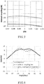
- FIG. 3 is an explanatory graph for showing the amount of mutual coupling in the array antenna device according to the first embodiment of the present invention by comparison between a case in which a coupling line is included and a case in which there is no coupling line.
- the axis of abscissa indicates a frequency standardized by the design center frequency
- the axis of ordinate indicates the amount of mutual coupling between the first patch antenna 10 and the second patch antenna 20.
- the amount of mutual coupling in the case where no coupling lines 30 are included is represented by the broken line in FIG. 3 , and is -18.1 dB.
- the amount of mutual coupling in the case where the coupling lines 30 are included is represented by the solid line in FIG. 3 , and is -26.1 dB.
- the comparison of the amount of mutual coupling between those cases reveals that mutual coupling is successfully reduced by 8.0 dB from the case of the related art in which there are no coupling lines 30.
- FIG. 4 is an explanatory graph for showing an emission pattern in the array antenna device according to the first embodiment of the present invention by comparison between a case in which a single patch antenna is used, a case in which a coupling line is included, and a case in which there is no coupling line.
- the axis of abscissa indicates the angle
- the axis of ordinate indicates an emission pattern observed when the first patch antenna 10 is excited.
- Patterns shown in FIG. 4 are: an emission pattern observed when the first patch antenna 10 is used alone (the solid line); an emission pattern observed when the first patch antenna 10 is excited, the coaxial line 23 of the second patch antenna 20 is match-terminated, and there are no coupling lines 30 (the broken line) ; and an emission pattern observed when the first patch antenna 10 is excited, the coaxial line 23 of the second patch antenna 20 is match-terminated, and the coupling lines 30 are included (the dotted line).
- FIG. 5 is an explanatory graph for showing an emission pattern in the array antenna device according to the first embodiment of the present invention by comparison between a case in which a single patch antenna is used, a case in which a coupling line is included, and a case in which there is no coupling line.
- the axis of abscissa indicates the angle
- the axis of ordinate indicates an emission pattern observed when the second patch antenna 20 is excited.
- Patterns shown in FIG. 5 are: an emission pattern observed when the second patch antenna 20 is used alone (the solid line); an emission pattern observed when the second patch antenna 20 is excited, the coaxial line 13 of the first patch antenna 10 is match-terminated, and there are no coupling lines 30 (the broken line); and an emission pattern observed when the second patch antenna 20 is excited, the coaxial line 13 of the first patch antenna 10 is match-terminated, and the coupling lines 30 are included (the dotted line).
- the emission pattern observed when the first patch antenna 10 is excited and the coupling lines 30 are included has, around a boresight, ripples smaller than the ones when the first patch antenna 10 is excited and there are no coupling lines 30, and is accordingly similar to the emission pattern observed when the first patch antenna 10 is used alone.
- the emission pattern observed when the second patch antenna 20 is excited and the coupling lines 30 are included has smaller ripples around the boresight than when the second patch antenna 20 is excited and there are no coupling lines 30, and is similar to the emission pattern observed when the second patch antenna 20 is used alone.
- Disturbance caused in emission characteristics by mutual coupling between the first patch antenna 10 and the second patch antenna 20 can accordingly be ameliorated by reducing the influence of the mutual coupling between the patch antennas.
- Mutual coupling is accordingly reduced by controlling the phases of the electromagnetic waves, each of which is coupled to the patch antennas, through the amount of bend, that is, the line length, of the coupling line to cancel out the electromagnetic wave coupled to the patch elements via space and the electromagnetic wave coupled to the patch elements via the coupling line.
- the coupling line can be formed by etching in the same manufacturing step as the step of forming the patch elements of the patch antennas, which means no additional cost to form the coupling line.
- FIG. 6 is a plan view for illustrating an array antenna device according to a second embodiment of the present invention.
- an array antenna device 100A includes coupling lines 30A in place of the coupling lines 30 illustrated in FIG. 1 .
- the coupling lines 30A are each made up of a first parallel line 31, a second parallel line 32, and a bent line 33A.
- Each bent line 33A is a line connecting one first parallel line 31 and one second parallel line 32 to each other, and is bent in the shape of a meander between the patch element 11 and the patch element 21.
- the rest of the configuration is the same as the one described in the first embodiment with reference to FIG. 1 , and a description on the rest is omitted.
- the operation of the array antenna device 100A configured as above, too, is the same as the operation described in the first embodiment, and a description on the operation is omitted.
- FIG. 7 is an explanatory graph for showing the amount of mutual coupling in the array antenna device according to the second embodiment of the present invention by comparison between a case in which a coupling line is included and a case in which there is no coupling line.
- the axis of abscissa indicates a frequency standardized by the design center frequency
- the axis of ordinate indicates the amount of mutual coupling between the first patch antenna 10 and the second patch antenna 20.
- the amount of mutual coupling in the case where the coupling lines 30A are included and the amount of mutual coupling in the case where no coupling lines 30A are included are represented by the solid line and the broken line, respectively, in FIG. 7 .
- the comparison of the amount of mutual coupling between those cases reveals that mutual coupling is successfully reduced by 10 dB from the case in which there are no coupling lines 30A.
- FIG. 8 is an explanatory graph for showing an emission pattern in the array antenna device according to the second embodiment of the present invention by comparison between a case in which a single patch antenna is used, a case in which a coupling line is included, and a case in which there is no coupling line.
- the axis of abscissa indicates the angle
- the axis of ordinate indicates an emission pattern observed when the first patch antenna 10 is excited.
- Patterns shown in FIG. 8 are: an emission pattern observed when the first patch antenna 10 is used alone (the solid line); an emission pattern observed when the first patch antenna 10 is excited, the coaxial line 23 of the second patch antenna 20 is match-terminated, and there are no coupling lines 30A (the broken line) ; and an emission pattern observed when the first patch antenna 10 is excited, the coaxial line 23 of the second patch antenna 20 is match-terminated, and the coupling lines 30A are included (the dotted line).
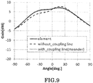
- FIG. 9 is an explanatory graph for showing an emission pattern in the array antenna device according to the second embodiment of the present invention by comparison between a case in which a single patch antenna is used, a case in which a coupling line is included, and a case in which there is no coupling line.
- the axis of abscissa indicates the angle
- the axis of ordinate indicates an emission pattern observed when the second patch antenna 20 is excited.
- Patterns shown in FIG. 9 are: an emission pattern observed when the second patch antenna 20 is used alone (the solid line); an emission pattern observed when the second patch antenna 20 is excited, the coaxial line 13 of the first patch antenna 10 is match-terminated, and there are no coupling lines 30A (the broken line); and an emission pattern observed when the second patch antenna 20 is excited, the coaxial line 13 of the first patch antenna 10 is match-terminated, and the coupling lines 30A are included (the dotted line).
- the emission pattern observed when the first patch antenna 10 is excited and the coupling lines 30A are included has, around a boresight, ripples smaller than the ones when the first patch antenna 10 is excited and there are no coupling lines 30A, and is accordingly similar to the emission pattern observed when the first patch antenna 10 is used alone.
- the emission pattern observed when the second patch antenna 20 is excited and the coupling lines 30A are included has smaller ripples around the boresight than when the second patch antenna 20 is excited and there are no coupling lines 30A, and is similar to the emission pattern observed when the second patch antenna 20 is used alone.
- Disturbance caused in emission characteristics by mutual coupling between the first patch antenna 10 and the second patch antenna 20 can accordingly be ameliorated by reducing the influence of the mutual coupling between the patch antennas.
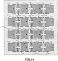
- FIG. 10 is another plan view for illustrating the array antenna device according to the second embodiment of the present invention, and patch antennas 40 are arrayed two-dimensionally into a 4 ⁇ 4 array in FIG. 10 .
- the coupling lines 30A in the second embodiment described above each have the bent line 33A, which is formed so as to be inserted between adjacent patch antennas 40.
- FIG. 11 to FIG. 17 are each a plan view for illustrating an array antenna device according to a third embodiment of the present invention. While the number and shape of the coupling lines are limited in the first embodiment and the second embodiment, the present invention is not limited thereto.
- one coupling line 30A may be formed between adjacent patch antennas 40 as illustrated in FIG. 11
- three or more coupling lines 30A and 50 may be formed between adjacent patch antennas 40 as illustrated in FIG. 12 .
- Coupling lines in the present invention do not always need to have a shape obtained by bending a straight line at the right angle, and can be like coupling lines 60 illustrated in FIG. 13 .
- Coupling lines in the present invention may also be shaped to have a bent portion made up of a curve as in the case of coupling lines 70 illustrated in FIG. 14 .
- the present invention is also not limited to the case described in the first embodiment and the second embodiment in which an array of patch antennas 40 is a two-dimensional array that is a two-element array or a quadrangular array.
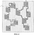
- the patch antennas 40 may form a linear array made up of three or more elements as illustrated in FIG. 15 , a triangular array as illustrated in FIG. 16 , and an aperiodic array as illustrated in FIG. 17 .
- the same effects as the ones described in the first embodiment and the second embodiment can be obtained by forming at least one coupling line between adjacent patch antennas 40 to cancel out the electromagnetic wave coupled via free space and the electromagnetic wave coupled via the coupling line.
- the wide range of choices in how the patch antennas 40 are arrayed and in the configuration of the coupling line also gives a degree of freedom to the designing of the array antenna device.
Landscapes
- Variable-Direction Aerials And Aerial Arrays (AREA)
- Waveguide Aerials (AREA)
- Details Of Aerials (AREA)
Abstract
Description
- The present invention relates to an array antenna device configured such that a planar antenna, such as a patch antenna, is used as an element antenna, and the element antennas are arrayed in plurality.
- Hitherto, a high level of transmission/reception of an electromagnetic wave from a varying arrival direction has been demanded of radars and mobile communication devices, and a method has been used in response to the demand which adopts an array antenna device including an array of a plurality of element antennas to control a main beam direction.
- In the array antenna device, the gap between adjacent element antennas in the array is required to be close in order to avoid unnecessary emission called grating lobe in the visible range in beam scanning.
- However, an array in which the gap between adjacent element antennas is close is high in the level of mutual coupling between the element antennas, and the resultant problems are low antenna gain and directivity disturbance.
- Various methods of reducing the mutual coupling between element antennas are disclosed for the purpose of solving those problems (see
Patent Literature 1 andPatent Literature 2, for example). - For instance, in a method disclosed in
Patent Literature 1, at least one of a metal body or a dielectric substance is formed in the vicinity of element antennas . InPatent Literature 2, there are disclosed a method in which each element antenna is covered with a metal wall and a method in which electromagnetic band gap (EBG) elements are arranged at equal intervals between element antennas. -
- [PTL 1]
JP 59-194517 A - [PTL 2]
JP 2010-28182 A -
Patent Literature 1, however, has a problem in that, while a description about providing a metal body and/or a dielectric substance in the vicinity of dipole antennas or circular horn antennas is included, there is no disclosure or even hint about the arrangement, specific structure, and the like of the metal body or the dielectric substance that reduce the mutual coupling when this method is applied to a patch antenna or a similar planar antenna. -
Patent Literature 2 has a problem as well because of the need for the metal wall, which is an additional member, and the need to form through-holes for arranging the EBG elements. The problem is a significant increase in cost due to the material cost required for the structure for reducing the mutual coupling, and an additional manufacturing cost for the added manufacturing step of forming the through-holes. - The present invention has been made to solve the problems described above, and an object of the present invention is therefore to provide an array antenna device capable of satisfactorily reducing mutual coupling between element antennas without inviting a significant increase in cost.
- According to one embodiment of the present invention, there is provided an array antenna device including a plurality of patch antennas arrayed in at least a polarization direction of the plurality of patch antennas, the array antenna device including: a parallel line formed for each of the plurality of patch antennas in parallel to the polarization direction of the patch antenna, on the same plane as a patch element of the patch antenna, close to the patch element and in a magnetic field direction of the patch antenna; and a bent line configured to connect the parallel line, which is formed close to the patch element, to another parallel line, which is formed close to another patch element, and shaped so as to be bent between adjacent patch elements, in which the parallel line and the bent line form a coupling line, which couples part of an electromagnetic wave excited by the patch element to an adjacent patch antenna, and in which, in the coupling line, a gap between the parallel line and the patch element and a length of the bent line are set so that an electromagnetic wave coupled from one patch antenna to an adjacent patch antenna via space and an electromagnetic wave coupled from the one patch antenna to the adjacent patch antenna via the coupling line cancel each other.
- According to the array antenna device of the present invention, the parallel line formed on the same plane as a patch element, close to the patch element, in a direction that is the magnetic field direction of the patch antenna and that is parallel to the polarization direction of the patch antenna, and the bent line shaped so as to be bent between adjacent patch elements and configured to connect their parallel lines to each other, form the coupling line, which couples part of an electromagnetic wave excited by one of the patch elements to its adjacent patch antenna, and, in the coupling line, a gap between the parallel line and the patch element and the length of the bent line are set so that an electromagnetic wave coupled from one patch antenna to its adjacent patch antenna via space and an electromagnetic wave coupled from the one patch antenna to the adjacent patch antenna via the coupling line cancel each other.
- Thus, it is possible to satisfactorily reduce mutual coupling between element antennas without inviting a significant increase in cost.
-
-
FIG. 1 is a plan view for illustrating an array antenna device according to a first embodiment of the present invention. -
FIG. 2 is a sectional view of the array antenna device ofFIG. 1 taken along the line I-I. -
FIG. 3 is an explanatory graph for showing the amount of mutual coupling in the array antenna device according to the first embodiment of the present invention by comparison between a case in which a coupling line is included and a case in which there is no coupling line. -
FIG. 4 is an explanatory graph for showing an emission pattern in the array antenna device according to the first embodiment of the present invention by comparison between a case in which a single patch antenna is used, a case in which a coupling line is included, and a case in which there is no coupling line. -
FIG. 5 is another explanatory graph for showing an emission pattern in the array antenna device according to the first embodiment of the present invention by comparison between a case in which a single patch antenna is used, a case in which a coupling line is included, and a case in which there is no coupling line. -
FIG. 6 is a plan view for illustrating an array antenna device according to a second embodiment of the present invention. -
FIG. 7 is an explanatory graph for showing the amount of mutual coupling in the array antenna device according to the second embodiment of the present invention by comparison between a case in which a coupling line is included and a case in which there is no coupling line. -
FIG. 8 is an explanatory graph for showing an emission pattern in the array antenna device according to the second embodiment of the present invention by comparison between a case in which a single patch antenna is used, a case in which a coupling line is included, and a case in which there is no coupling line. -
FIG. 9 is another explanatory graph for showing an emission pattern in the array antenna device according to the second embodiment of the present invention by comparison between a case in which a single patch antenna is used, a case in which a coupling line is included, and a case in which there is no coupling line. -
FIG. 10 is another plan view for illustrating the array antenna device according to the second embodiment of the present invention. -
FIG. 11 is a plan view for illustrating an array antenna device according to a third embodiment of the present invention. -
FIG. 12 is another plan view for illustrating the array antenna device according to the third embodiment of the present invention. -
FIG. 13 is still another plan view for illustrating the array antenna device according to the third embodiment of the present invention. -
FIG. 14 is yet still another plan view for illustrating the array antenna device according to the third embodiment of the present invention. -
FIG. 15 is yet still another plan view for illustrating the array antenna device according to the third embodiment of the present invention. -
FIG. 16 is yet still another plan view for illustrating the array antenna device according to the third embodiment of the present invention. -
FIG. 17 is yet still another plan view for illustrating the array antenna device according to the third embodiment of the present invention. - A description is now given of an array antenna device according to preferred embodiments of the present invention referring to the accompanying drawings, and throughout the drawings, like or corresponding components are denoted by like reference symbols to describe those components.
-
FIG. 1 is a plan view for illustrating an array antenna device according to a first embodiment of the present invention.FIG. 2 is a sectional view of the array antenna device ofFIG. 1 taken along the line I-I. InFIG. 1 and FIG. 2 , anarray antenna device 100 includes afirst patch antenna 10 and asecond patch antenna 20, which are formed on adielectric substrate 1, and twocoupling lines 30 as well. - The
first patch antenna 10 includes apatch element 11, which is formed on thedielectric substrate 1, apower feeding probe 12 and acoaxial line 13, which excite thepatch element 11, and aground plane 2, which is formed on a flat surface of thedielectric substrate 1 on the side opposite from thepatch element 11. - Further, the
second patch antenna 20 includes apatch element 21, which is formed on thedielectric substrate 1, apower feeding probe 22 and acoaxial line 23, which excite thepatch element 21, and theground plane 2. - The
first patch antenna 10 and thesecond patch antenna 20 are arrayed so as to be adjacent to each other in a direction that is the polarization direction of thefirst patch antenna 10 and thesecond patch antenna 20. This makes the array of thefirst patch antenna 10 and thesecond patch antenna 20 an E-plane array. - The two
coupling lines 30 are formed so as to be symmetrical with respect to the line I-I inFIG. 1 , which passes through centers of thepatch elements coupling lines 30 are each made up of a firstparallel line 31, a secondparallel line 32, and abent line 33. - Each first
parallel line 31 is formed close to thepatch element 11 on thedielectric substrate 1 in a magnetic field direction of thefirst patch antenna 10 and thesecond patch antenna 20. Each firstparallel line 31 is also a line formed in parallel to the polarization direction of thefirst patch antenna 10 and thesecond patch antenna 20. - Further, each second
parallel line 32 is formed close to thepatch element 21 on thedielectric substrate 1 in the magnetic field direction of thefirst patch antenna 20 and thesecond patch antenna 20. Each secondparallel line 32 is also a line formed in parallel to the polarization direction of thefirst patch antenna 10 and thesecond patch antenna 20. - Each
bent line 33 is a line connecting one firstparallel line 31 and one secondparallel line 32 to each other, and is bent in the shape of a crank between thepatch element 11 and thepatch element 21. - The operation of the
array antenna device 100 configured as above is described below. First, an electromagnetic wave excited by thepatch element 11 via thepower feeding probe 12 and thecoaxial line 13, namely, an electromagnetic wave resultant from the excitation of thefirst patch antenna 10, is mostly emitted into free space. - Part of the electromagnetic wave excited by the
patch element 11 is coupled to thecoupling lines 30 in thearray antenna device 100 configured as above because each firstparallel line 31 is formed on the same plane as thepatch element 11, close to thepatch element 11, in a direction that is the magnetic field direction of thefirst patch antenna 10 and that is parallel to the polarization direction of thefirst patch antenna 10. - Part of the electromagnetic wave emitted into free space is coupled via free space to the
second patch antenna 20 adjacent to thefirst patch antenna 10. Part of the electromagnetic wave coupled to thecoupling lines 30, too, is coupled via thecoupling lines 30 to the adjacentsecond patch antenna 20. - In the array antenna device according to the first embodiment of the present invention, it is desirable to set the length of each of the
coupling lines 30 so that the electromagnetic wave coupled from thefirst patch antenna 10 to thesecond patch antenna 20 via free space and the electromagnetic wave coupled from thefirst patch antenna 10 to thesecond patch antenna 20 via thecoupling lines 30 cancel each other. - Specifically, the gap from the
patch element 11 to one firstparallel line 31 and one secondparallel line 32, the gap from thepatch element 21 to another firstparallel line 31 and another secondparallel line 32, and the length of eachbent line 33 are set so that the electromagnetic wave coupled from thefirst patch antenna 10 to thesecond patch antenna 20 via free space and the electromagnetic wave coupled from thefirst patch antenna 10 to thesecond patch antenna 20 via thecoupling lines 30 have roughly equal amplitudes and phases reverse to each other. - An electromagnetic wave coupled from the
second patch antenna 20 to thefirst patch antenna 10 at this point is similar to the electromagnetic wave coupled from thefirst patch antenna 10 to thesecond patch antenna 20 due to reversibility. Mutual coupling between thefirst patch antenna 10 and thesecond patch antenna 20 can accordingly be reduced. - Effects of the
array antenna device 100 according to the first embodiment of the present invention are described below by comparison of the amount of mutual coupling between a case in which thecoupling lines 30 are included and a case in which there is no coupling line, while giving a calculation example. - In the calculation, the gap between the
first patch antenna 10 and thesecond patch antenna 20 is set to 1/2 of the free space wavelength, and the length of each side of the shape of thepatch elements patch elements -
FIG. 3 is an explanatory graph for showing the amount of mutual coupling in the array antenna device according to the first embodiment of the present invention by comparison between a case in which a coupling line is included and a case in which there is no coupling line. InFIG. 3 , the axis of abscissa indicates a frequency standardized by the design center frequency, and the axis of ordinate indicates the amount of mutual coupling between thefirst patch antenna 10 and thesecond patch antenna 20. - The amount of mutual coupling in the case where no
coupling lines 30 are included is represented by the broken line inFIG. 3 , and is -18.1 dB. The amount of mutual coupling in the case where thecoupling lines 30 are included is represented by the solid line inFIG. 3 , and is -26.1 dB. The comparison of the amount of mutual coupling between those cases reveals that mutual coupling is successfully reduced by 8.0 dB from the case of the related art in which there are no coupling lines 30. -
FIG. 4 is an explanatory graph for showing an emission pattern in the array antenna device according to the first embodiment of the present invention by comparison between a case in which a single patch antenna is used, a case in which a coupling line is included, and a case in which there is no coupling line. InFIG. 4 , the axis of abscissa indicates the angle, and the axis of ordinate indicates an emission pattern observed when thefirst patch antenna 10 is excited. - Patterns shown in
FIG. 4 are: an emission pattern observed when thefirst patch antenna 10 is used alone (the solid line); an emission pattern observed when thefirst patch antenna 10 is excited, thecoaxial line 23 of thesecond patch antenna 20 is match-terminated, and there are no coupling lines 30 (the broken line) ; and an emission pattern observed when thefirst patch antenna 10 is excited, thecoaxial line 23 of thesecond patch antenna 20 is match-terminated, and thecoupling lines 30 are included (the dotted line). -
FIG. 5 is an explanatory graph for showing an emission pattern in the array antenna device according to the first embodiment of the present invention by comparison between a case in which a single patch antenna is used, a case in which a coupling line is included, and a case in which there is no coupling line. InFIG. 5 , the axis of abscissa indicates the angle, and the axis of ordinate indicates an emission pattern observed when thesecond patch antenna 20 is excited. - Patterns shown in
FIG. 5 are: an emission pattern observed when thesecond patch antenna 20 is used alone (the solid line); an emission pattern observed when thesecond patch antenna 20 is excited, thecoaxial line 13 of thefirst patch antenna 10 is match-terminated, and there are no coupling lines 30 (the broken line); and an emission pattern observed when thesecond patch antenna 20 is excited, thecoaxial line 13 of thefirst patch antenna 10 is match-terminated, and thecoupling lines 30 are included (the dotted line). - It is understood from
FIG. 4 that the emission pattern observed when thefirst patch antenna 10 is excited and thecoupling lines 30 are included has, around a boresight, ripples smaller than the ones when thefirst patch antenna 10 is excited and there are nocoupling lines 30, and is accordingly similar to the emission pattern observed when thefirst patch antenna 10 is used alone. - From
FIG. 5 , it is understood that, as is the case for the emission patterns observed when thefirst patch antenna 10 is excited, the emission pattern observed when thesecond patch antenna 20 is excited and thecoupling lines 30 are included has smaller ripples around the boresight than when thesecond patch antenna 20 is excited and there are nocoupling lines 30, and is similar to the emission pattern observed when thesecond patch antenna 20 is used alone. - Disturbance caused in emission characteristics by mutual coupling between the
first patch antenna 10 and thesecond patch antenna 20 can accordingly be ameliorated by reducing the influence of the mutual coupling between the patch antennas. - As described above, according to the first embodiment, the parallel line formed on the same plane as a patch element, close to the patch element, in a direction that is the magnetic field direction of the patch antenna and that is parallel to the polarization direction of the patch antenna, and the bent line shaped so as to be bent between adjacent patch elements and configured to connect their parallel lines to each other, form the coupling line, which couples part of an electromagnetic wave excited by one of the patch elements to its adjacent patch antenna, and, in the coupling line, a gap between the parallel line and the patch element and the length of the bent line are set so that an electromagnetic wave coupled from one patch antenna to its adjacent patch antenna via space and an electromagnetic wave coupled from the one patch antenna to the adjacent patch antenna via the coupling line cancel each other.
- Mutual coupling is accordingly reduced by controlling the phases of the electromagnetic waves, each of which is coupled to the patch antennas, through the amount of bend, that is, the line length, of the coupling line to cancel out the electromagnetic wave coupled to the patch elements via space and the electromagnetic wave coupled to the patch elements via the coupling line.
- Another advantage is that the coupling line can be formed by etching in the same manufacturing step as the step of forming the patch elements of the patch antennas, which means no additional cost to form the coupling line.
- Mutual coupling between element antennas can thus be reduced satisfactorily without inviting a significant increase in cost.
-
FIG. 6 is a plan view for illustrating an array antenna device according to a second embodiment of the present invention. InFIG. 6 , anarray antenna device 100A includescoupling lines 30A in place of thecoupling lines 30 illustrated inFIG. 1 . - The coupling lines 30A are each made up of a first
parallel line 31, a secondparallel line 32, and abent line 33A. Eachbent line 33A is a line connecting one firstparallel line 31 and one secondparallel line 32 to each other, and is bent in the shape of a meander between thepatch element 11 and thepatch element 21. - The rest of the configuration is the same as the one described in the first embodiment with reference to
FIG. 1 , and a description on the rest is omitted. The operation of thearray antenna device 100A configured as above, too, is the same as the operation described in the first embodiment, and a description on the operation is omitted. - Effects of the
array antenna device 100A according to the second embodiment of the present invention are described below by comparison of the amount of mutual coupling between a case in which thecoupling lines 30A are included and a case in which there is no coupling line, while giving a calculation example. Conditions of the calculation are the same as those in the first embodiment described above. -
FIG. 7 is an explanatory graph for showing the amount of mutual coupling in the array antenna device according to the second embodiment of the present invention by comparison between a case in which a coupling line is included and a case in which there is no coupling line. InFIG. 7 , the axis of abscissa indicates a frequency standardized by the design center frequency, and the axis of ordinate indicates the amount of mutual coupling between thefirst patch antenna 10 and thesecond patch antenna 20. - The amount of mutual coupling in the case where the
coupling lines 30A are included and the amount of mutual coupling in the case where nocoupling lines 30A are included are represented by the solid line and the broken line, respectively, inFIG. 7 . The comparison of the amount of mutual coupling between those cases reveals that mutual coupling is successfully reduced by 10 dB from the case in which there are nocoupling lines 30A. -
FIG. 8 is an explanatory graph for showing an emission pattern in the array antenna device according to the second embodiment of the present invention by comparison between a case in which a single patch antenna is used, a case in which a coupling line is included, and a case in which there is no coupling line. InFIG. 8 , the axis of abscissa indicates the angle, and the axis of ordinate indicates an emission pattern observed when thefirst patch antenna 10 is excited. - Patterns shown in
FIG. 8 are: an emission pattern observed when thefirst patch antenna 10 is used alone (the solid line); an emission pattern observed when thefirst patch antenna 10 is excited, thecoaxial line 23 of thesecond patch antenna 20 is match-terminated, and there are nocoupling lines 30A (the broken line) ; and an emission pattern observed when thefirst patch antenna 10 is excited, thecoaxial line 23 of thesecond patch antenna 20 is match-terminated, and thecoupling lines 30A are included (the dotted line). -
FIG. 9 is an explanatory graph for showing an emission pattern in the array antenna device according to the second embodiment of the present invention by comparison between a case in which a single patch antenna is used, a case in which a coupling line is included, and a case in which there is no coupling line. InFIG. 9 , the axis of abscissa indicates the angle, and the axis of ordinate indicates an emission pattern observed when thesecond patch antenna 20 is excited. - Patterns shown in
FIG. 9 are: an emission pattern observed when thesecond patch antenna 20 is used alone (the solid line); an emission pattern observed when thesecond patch antenna 20 is excited, thecoaxial line 13 of thefirst patch antenna 10 is match-terminated, and there are nocoupling lines 30A (the broken line); and an emission pattern observed when thesecond patch antenna 20 is excited, thecoaxial line 13 of thefirst patch antenna 10 is match-terminated, and thecoupling lines 30A are included (the dotted line). - It is understood from
FIG. 8 that the emission pattern observed when thefirst patch antenna 10 is excited and thecoupling lines 30A are included has, around a boresight, ripples smaller than the ones when thefirst patch antenna 10 is excited and there are nocoupling lines 30A, and is accordingly similar to the emission pattern observed when thefirst patch antenna 10 is used alone. - From
FIG. 9 , it is understood that, as is the case for the emission patterns observed when thefirst patch antenna 10 is excited, the emission pattern observed when thesecond patch antenna 20 is excited and thecoupling lines 30A are included has smaller ripples around the boresight than when thesecond patch antenna 20 is excited and there are nocoupling lines 30A, and is similar to the emission pattern observed when thesecond patch antenna 20 is used alone. - Disturbance caused in emission characteristics by mutual coupling between the
first patch antenna 10 and thesecond patch antenna 20 can accordingly be ameliorated by reducing the influence of the mutual coupling between the patch antennas. - According to the second embodiment, mutual coupling between element antennas can thus be reduced satisfactorily without inviting a significant increase in cost, as in the first embodiment described above.
-
FIG. 10 is another plan view for illustrating the array antenna device according to the second embodiment of the present invention, andpatch antennas 40 are arrayed two-dimensionally into a 4×4 array inFIG. 10 . The coupling lines 30A in the second embodiment described above each have thebent line 33A, which is formed so as to be inserted betweenadjacent patch antennas 40. - Accordingly, it is physically possible to array the
coupling lines 30A even when, for example, thepatch antennas 40, from which thearray antenna device 100 is formed, form a two-dimensional array with a narrow gap from one another as illustrated inFIG. 10 , and mutual coupling betweenadjacent patch antennas 40 is reduced as a result. -
FIG. 11 to FIG. 17 are each a plan view for illustrating an array antenna device according to a third embodiment of the present invention. While the number and shape of the coupling lines are limited in the first embodiment and the second embodiment, the present invention is not limited thereto. - For instance, one
coupling line 30A may be formed betweenadjacent patch antennas 40 as illustrated inFIG. 11 , and three ormore coupling lines adjacent patch antennas 40 as illustrated inFIG. 12 . - Coupling lines in the present invention do not always need to have a shape obtained by bending a straight line at the right angle, and can be like coupling
lines 60 illustrated inFIG. 13 . Coupling lines in the present invention may also be shaped to have a bent portion made up of a curve as in the case ofcoupling lines 70 illustrated inFIG. 14 . - The present invention is also not limited to the case described in the first embodiment and the second embodiment in which an array of
patch antennas 40 is a two-dimensional array that is a two-element array or a quadrangular array. For instance, thepatch antennas 40 may form a linear array made up of three or more elements as illustrated inFIG. 15 , a triangular array as illustrated inFIG. 16 , and an aperiodic array as illustrated inFIG. 17 . - In those cases, too, the same effects as the ones described in the first embodiment and the second embodiment can be obtained by forming at least one coupling line between
adjacent patch antennas 40 to cancel out the electromagnetic wave coupled via free space and the electromagnetic wave coupled via the coupling line. The wide range of choices in how thepatch antennas 40 are arrayed and in the configuration of the coupling line also gives a degree of freedom to the designing of the array antenna device.
Claims (8)
- An array antenna device including a plurality of patch antennas arrayed in at least a polarization direction of the plurality of patch antennas,
the array antenna device comprising:a parallel line formed for each of the plurality of patch antennas in parallel to the polarization direction of the patch antenna, on the same plane as a patch element of the patch antenna, close to the patch element and in a magnetic field direction of the patch antenna; anda bent line configured to connect the parallel line, which is formed close to the patch element, to another parallel line, which is formed close to another patch element, and shaped so as to be bent between adjacent patch elements,wherein the parallel line and the bent line form a coupling line, which couples part of an electromagnetic wave excited by the patch element to an adjacent patch antenna, andwherein, in the coupling line, a gap between the parallel line and the patch element and a length of the bent line are set so that an electromagnetic wave coupled from one patch antenna to an adjacent patch antenna via space and an electromagnetic wave coupled from the one patch antenna to the adjacent patch antenna via the coupling line cancel each other. - An array antenna device according to claim 1, wherein the bent line is bent in a shape of a crank.
- An array antenna device according to claim 1, wherein the bent line is bent in a shape of a meander.
- An array antenna device according to claim 1, wherein the bent line is bent in a shape of a curve.
- An array antenna device according to any one of claims 1 to 4, wherein at least two coupling lines are formed in the magnetic field direction of the patch antenna.
- An array antenna device according to any one of claims 1 to 5, wherein the plurality of patch antennas are arrayed into a quadrangular array.
- An array antenna device according to any one of claims 1 to 5, wherein the plurality of patch antennas are arrayed into a triangular array.
- An array antenna device according to any one of claims 1 to 5, wherein the plurality of patch antennas are arrayed into an aperiodic array.
Applications Claiming Priority (1)
| Application Number | Priority Date | Filing Date | Title |
|---|---|---|---|
| PCT/JP2016/067668 WO2017216871A1 (en) | 2016-06-14 | 2016-06-14 | Array antenna device |
Publications (3)
| Publication Number | Publication Date |
|---|---|
| EP3460907A1 true EP3460907A1 (en) | 2019-03-27 |
| EP3460907A4 EP3460907A4 (en) | 2019-06-05 |
| EP3460907B1 EP3460907B1 (en) | 2021-10-13 |
Family
ID=60663967
Family Applications (1)
| Application Number | Title | Priority Date | Filing Date |
|---|---|---|---|
| EP16905426.9A Active EP3460907B1 (en) | 2016-06-14 | 2016-06-14 | Array antenna device |
Country Status (5)
| Country | Link |
|---|---|
| US (1) | US20190131701A1 (en) |
| EP (1) | EP3460907B1 (en) |
| JP (1) | JP6395984B2 (en) |
| CN (1) | CN109314313B (en) |
| WO (1) | WO2017216871A1 (en) |
Families Citing this family (14)
| Publication number | Priority date | Publication date | Assignee | Title |
|---|---|---|---|---|
| US11005174B2 (en) * | 2016-06-15 | 2021-05-11 | University Of Florida Research Foundation, Incorporated | Point symmetric complementary meander line slots for mutual coupling reduction |
| EP3616255B8 (en) * | 2017-04-25 | 2023-10-25 | The Antenna Company International N.V. | Ebg structure, ebg component, and antenna device |
| CN108281788A (en) * | 2018-01-22 | 2018-07-13 | 电子科技大学 | A kind of element microstrip array antenna reducing coupling |
| KR102639417B1 (en) | 2019-05-10 | 2024-02-23 | 삼성전자주식회사 | Electronic device including antenna |
| EP3993161A4 (en) * | 2019-06-25 | 2023-07-26 | Kyocera Corporation | Antenna, wireless communication module, and wireless communication device |
| WO2021000175A1 (en) * | 2019-06-30 | 2021-01-07 | 瑞声声学科技(深圳)有限公司 | Antenna and base station |
| TWI738343B (en) * | 2020-05-18 | 2021-09-01 | 為昇科科技股份有限公司 | Meander antenna structure |
| KR20220068557A (en) * | 2020-11-19 | 2022-05-26 | 삼성전기주식회사 | Antenna apparatus |
| JP7771979B2 (en) * | 2020-12-24 | 2025-11-18 | Agc株式会社 | Antenna device and vehicle antenna system |
| EP4040602B1 (en) * | 2021-02-08 | 2025-03-05 | Nokia Technologies Oy | An array of patch antennas |
| US12132250B2 (en) | 2021-09-15 | 2024-10-29 | Samsung Electronics Co., Ltd. | Antenna module and electronic device including the same |
| CN116130956A (en) * | 2021-11-15 | 2023-05-16 | 华为技术有限公司 | Decoupling antenna array and decoupling device |
| WO2023095223A1 (en) * | 2021-11-24 | 2023-06-01 | エイターリンク株式会社 | Wireless power supply device |
| CN114267946B (en) * | 2021-12-16 | 2025-08-05 | Oppo广东移动通信有限公司 | Antenna assembly and electronic equipment |
Family Cites Families (19)
| Publication number | Priority date | Publication date | Assignee | Title |
|---|---|---|---|---|
| US5892482A (en) * | 1996-12-06 | 1999-04-06 | Raytheon Company | Antenna mutual coupling neutralizer |
| SE9700401D0 (en) * | 1997-02-05 | 1997-02-05 | Allgon Ab | Antenna operating with isolated channels |
| SE519118C2 (en) * | 1997-07-23 | 2003-01-14 | Allgon Ab | Antenna device for receiving and / or transmitting double-polarizing electromagnetic waves |
| SE512413C2 (en) * | 1997-10-01 | 2000-03-13 | Allgon Ab | Methods of manufacturing an antenna device and antenna device |
| US6320542B1 (en) * | 1998-09-22 | 2001-11-20 | Matsushita Electric Industrial Co., Ltd. | Patch antenna apparatus with improved projection area |
| KR100699472B1 (en) * | 2005-09-27 | 2007-03-26 | 삼성전자주식회사 | Flat Panel Array Antenna with Isolation Element |
| US20070279286A1 (en) * | 2006-06-05 | 2007-12-06 | Mark Iv Industries Corp. | Multi-Mode Antenna Array |
| FR2942915A1 (en) * | 2009-03-06 | 2010-09-10 | Thomson Licensing | COMPACT ANTENNA SYSTEM |
| KR101139703B1 (en) * | 2010-11-23 | 2012-04-26 | 주식회사 모비텍 | Mimo antenna having multi-isolation element |
| CN102104185A (en) * | 2010-12-01 | 2011-06-22 | 中兴通讯股份有限公司 | Multiple input multiple output (MIMO) array antenna |
| US8890763B2 (en) * | 2011-02-21 | 2014-11-18 | Funai Electric Co., Ltd. | Multiantenna unit and communication apparatus |
| CN102280696A (en) * | 2011-04-28 | 2011-12-14 | 上海交通大学 | Half-wave transmission decoupling small-space microstrip array antenna |
| US9444129B2 (en) * | 2011-05-13 | 2016-09-13 | Funai Electric Co., Ltd. | Multi-band compatible multi-antenna device and communication equipment |
| TWI502810B (en) * | 2012-05-25 | 2015-10-01 | Acer Inc | Communication device |
| CN103457037A (en) * | 2012-05-30 | 2013-12-18 | 宏碁股份有限公司 | Communication device |
| CN203103510U (en) * | 2012-09-27 | 2013-07-31 | 东莞宇龙通信科技有限公司 | MIMO antenna device and communication terminal with MIMO antenna device |
| TW201442340A (en) * | 2013-04-18 | 2014-11-01 | Ind Tech Res Inst | Multi-antenna system |
| TWI539674B (en) * | 2014-09-26 | 2016-06-21 | 宏碁股份有限公司 | Antenna system |
| TW201712950A (en) * | 2015-09-23 | 2017-04-01 | 啟碁科技股份有限公司 | Antenna system |
-
2016
- 2016-06-14 US US16/096,408 patent/US20190131701A1/en not_active Abandoned
- 2016-06-14 JP JP2018523076A patent/JP6395984B2/en active Active
- 2016-06-14 CN CN201680086506.6A patent/CN109314313B/en active Active
- 2016-06-14 WO PCT/JP2016/067668 patent/WO2017216871A1/en not_active Ceased
- 2016-06-14 EP EP16905426.9A patent/EP3460907B1/en active Active
Also Published As
| Publication number | Publication date |
|---|---|
| WO2017216871A1 (en) | 2017-12-21 |
| US20190131701A1 (en) | 2019-05-02 |
| JP6395984B2 (en) | 2018-09-26 |
| JPWO2017216871A1 (en) | 2018-09-27 |
| EP3460907B1 (en) | 2021-10-13 |
| CN109314313B (en) | 2021-07-23 |
| CN109314313A (en) | 2019-02-05 |
| EP3460907A4 (en) | 2019-06-05 |
Similar Documents
| Publication | Publication Date | Title |
|---|---|---|
| EP3460907B1 (en) | Array antenna device | |
| US9692117B2 (en) | Antenna | |
| US9929472B2 (en) | Phased array antenna | |
| EP2493018B1 (en) | Aperture mode filter | |
| US8144068B2 (en) | To planar antennas comprising at least one radiating element of the longitudinal radiation slot type | |
| US20200091599A1 (en) | Antenna device | |
| EP3038206B1 (en) | Augmented e-plane taper techniques in variable inclination continuous transverse stub antenna arrays | |
| JP2016058790A (en) | Array antenna and device using the same | |
| JP2011244136A (en) | Antenna device | |
| EP3780279A1 (en) | Array antenna apparatus and communication device | |
| GB2539279A (en) | Frequency selective surface for reducing antenna coupling | |
| EP4407786A2 (en) | High-performance dual-polarized antenna feed chain | |
| JP2017059909A (en) | Waveguide/transmission line converter, array antenna and plane antenna | |
| EP3059802B1 (en) | Array antenna | |
| US11189939B2 (en) | Dual-polarized wide-bandwidth antenna | |
| Mologni et al. | Investigation on the deployment of FSS as electromagnetic shielding for 5G devices | |
| JP6721352B2 (en) | Waveguide/transmission line converter and antenna device | |
| Wei et al. | Array-antenna decoupling surfaces for quasi-yagi antenna arrays | |
| EP3312934A1 (en) | Antenna | |
| BG et al. | Multi-band Series-Fed Millimeter Wave Array Antenna with LP and CP Characteristics for 5G Applications | |
| KR101775516B1 (en) | Crpa array antenna | |
| KR102324090B1 (en) | Dipole Communication Antenna for Integrated Mast | |
| CN112821058B (en) | A Vivaldi antenna | |
| JP2013110577A (en) | Antenna, array antenna and sector antenna | |
| KR20110116834A (en) | Linear tapered slot antenna with slot and array antenna |
Legal Events
| Date | Code | Title | Description |
|---|---|---|---|
| STAA | Information on the status of an ep patent application or granted ep patent |
Free format text: STATUS: THE INTERNATIONAL PUBLICATION HAS BEEN MADE |
|
| PUAI | Public reference made under article 153(3) epc to a published international application that has entered the european phase |
Free format text: ORIGINAL CODE: 0009012 |
|
| STAA | Information on the status of an ep patent application or granted ep patent |
Free format text: STATUS: REQUEST FOR EXAMINATION WAS MADE |
|
| 17P | Request for examination filed |
Effective date: 20181210 |
|
| AK | Designated contracting states |
Kind code of ref document: A1 Designated state(s): AL AT BE BG CH CY CZ DE DK EE ES FI FR GB GR HR HU IE IS IT LI LT LU LV MC MK MT NL NO PL PT RO RS SE SI SK SM TR |
|
| AX | Request for extension of the european patent |
Extension state: BA ME |
|
| A4 | Supplementary search report drawn up and despatched |
Effective date: 20190507 |
|
| RIC1 | Information provided on ipc code assigned before grant |
Ipc: H01Q 1/52 20060101AFI20190430BHEP Ipc: H01Q 21/06 20060101ALI20190430BHEP Ipc: H01Q 13/08 20060101ALI20190430BHEP |
|
| DAV | Request for validation of the european patent (deleted) | ||
| DAX | Request for extension of the european patent (deleted) | ||
| GRAP | Despatch of communication of intention to grant a patent |
Free format text: ORIGINAL CODE: EPIDOSNIGR1 |
|
| STAA | Information on the status of an ep patent application or granted ep patent |
Free format text: STATUS: GRANT OF PATENT IS INTENDED |
|
| INTG | Intention to grant announced |
Effective date: 20210429 |
|
| GRAS | Grant fee paid |
Free format text: ORIGINAL CODE: EPIDOSNIGR3 |
|
| GRAA | (expected) grant |
Free format text: ORIGINAL CODE: 0009210 |
|
| STAA | Information on the status of an ep patent application or granted ep patent |
Free format text: STATUS: THE PATENT HAS BEEN GRANTED |
|
| AK | Designated contracting states |
Kind code of ref document: B1 Designated state(s): AL AT BE BG CH CY CZ DE DK EE ES FI FR GB GR HR HU IE IS IT LI LT LU LV MC MK MT NL NO PL PT RO RS SE SI SK SM TR |
|
| REG | Reference to a national code |
Ref country code: GB Ref legal event code: FG4D |
|
| REG | Reference to a national code |
Ref country code: CH Ref legal event code: EP |
|
| REG | Reference to a national code |
Ref country code: DE Ref legal event code: R096 Ref document number: 602016065015 Country of ref document: DE |
|
| REG | Reference to a national code |
Ref country code: IE Ref legal event code: FG4D |
|
| REG | Reference to a national code |
Ref country code: AT Ref legal event code: REF Ref document number: 1438851 Country of ref document: AT Kind code of ref document: T Effective date: 20211115 |
|
| REG | Reference to a national code |
Ref country code: LT Ref legal event code: MG9D |
|
| REG | Reference to a national code |
Ref country code: NL Ref legal event code: MP Effective date: 20211013 |
|
| REG | Reference to a national code |
Ref country code: AT Ref legal event code: MK05 Ref document number: 1438851 Country of ref document: AT Kind code of ref document: T Effective date: 20211013 |
|
| PG25 | Lapsed in a contracting state [announced via postgrant information from national office to epo] |
Ref country code: RS Free format text: LAPSE BECAUSE OF FAILURE TO SUBMIT A TRANSLATION OF THE DESCRIPTION OR TO PAY THE FEE WITHIN THE PRESCRIBED TIME-LIMIT Effective date: 20211013 Ref country code: LT Free format text: LAPSE BECAUSE OF FAILURE TO SUBMIT A TRANSLATION OF THE DESCRIPTION OR TO PAY THE FEE WITHIN THE PRESCRIBED TIME-LIMIT Effective date: 20211013 Ref country code: FI Free format text: LAPSE BECAUSE OF FAILURE TO SUBMIT A TRANSLATION OF THE DESCRIPTION OR TO PAY THE FEE WITHIN THE PRESCRIBED TIME-LIMIT Effective date: 20211013 Ref country code: BG Free format text: LAPSE BECAUSE OF FAILURE TO SUBMIT A TRANSLATION OF THE DESCRIPTION OR TO PAY THE FEE WITHIN THE PRESCRIBED TIME-LIMIT Effective date: 20220113 Ref country code: AT Free format text: LAPSE BECAUSE OF FAILURE TO SUBMIT A TRANSLATION OF THE DESCRIPTION OR TO PAY THE FEE WITHIN THE PRESCRIBED TIME-LIMIT Effective date: 20211013 |
|
| PG25 | Lapsed in a contracting state [announced via postgrant information from national office to epo] |
Ref country code: IS Free format text: LAPSE BECAUSE OF FAILURE TO SUBMIT A TRANSLATION OF THE DESCRIPTION OR TO PAY THE FEE WITHIN THE PRESCRIBED TIME-LIMIT Effective date: 20220213 Ref country code: SE Free format text: LAPSE BECAUSE OF FAILURE TO SUBMIT A TRANSLATION OF THE DESCRIPTION OR TO PAY THE FEE WITHIN THE PRESCRIBED TIME-LIMIT Effective date: 20211013 Ref country code: PT Free format text: LAPSE BECAUSE OF FAILURE TO SUBMIT A TRANSLATION OF THE DESCRIPTION OR TO PAY THE FEE WITHIN THE PRESCRIBED TIME-LIMIT Effective date: 20220214 Ref country code: PL Free format text: LAPSE BECAUSE OF FAILURE TO SUBMIT A TRANSLATION OF THE DESCRIPTION OR TO PAY THE FEE WITHIN THE PRESCRIBED TIME-LIMIT Effective date: 20211013 Ref country code: NO Free format text: LAPSE BECAUSE OF FAILURE TO SUBMIT A TRANSLATION OF THE DESCRIPTION OR TO PAY THE FEE WITHIN THE PRESCRIBED TIME-LIMIT Effective date: 20220113 Ref country code: NL Free format text: LAPSE BECAUSE OF FAILURE TO SUBMIT A TRANSLATION OF THE DESCRIPTION OR TO PAY THE FEE WITHIN THE PRESCRIBED TIME-LIMIT Effective date: 20211013 Ref country code: LV Free format text: LAPSE BECAUSE OF FAILURE TO SUBMIT A TRANSLATION OF THE DESCRIPTION OR TO PAY THE FEE WITHIN THE PRESCRIBED TIME-LIMIT Effective date: 20211013 Ref country code: HR Free format text: LAPSE BECAUSE OF FAILURE TO SUBMIT A TRANSLATION OF THE DESCRIPTION OR TO PAY THE FEE WITHIN THE PRESCRIBED TIME-LIMIT Effective date: 20211013 Ref country code: GR Free format text: LAPSE BECAUSE OF FAILURE TO SUBMIT A TRANSLATION OF THE DESCRIPTION OR TO PAY THE FEE WITHIN THE PRESCRIBED TIME-LIMIT Effective date: 20220114 Ref country code: ES Free format text: LAPSE BECAUSE OF FAILURE TO SUBMIT A TRANSLATION OF THE DESCRIPTION OR TO PAY THE FEE WITHIN THE PRESCRIBED TIME-LIMIT Effective date: 20211013 |
|
| REG | Reference to a national code |
Ref country code: DE Ref legal event code: R097 Ref document number: 602016065015 Country of ref document: DE |
|
| PG25 | Lapsed in a contracting state [announced via postgrant information from national office to epo] |
Ref country code: SM Free format text: LAPSE BECAUSE OF FAILURE TO SUBMIT A TRANSLATION OF THE DESCRIPTION OR TO PAY THE FEE WITHIN THE PRESCRIBED TIME-LIMIT Effective date: 20211013 Ref country code: SK Free format text: LAPSE BECAUSE OF FAILURE TO SUBMIT A TRANSLATION OF THE DESCRIPTION OR TO PAY THE FEE WITHIN THE PRESCRIBED TIME-LIMIT Effective date: 20211013 Ref country code: RO Free format text: LAPSE BECAUSE OF FAILURE TO SUBMIT A TRANSLATION OF THE DESCRIPTION OR TO PAY THE FEE WITHIN THE PRESCRIBED TIME-LIMIT Effective date: 20211013 Ref country code: EE Free format text: LAPSE BECAUSE OF FAILURE TO SUBMIT A TRANSLATION OF THE DESCRIPTION OR TO PAY THE FEE WITHIN THE PRESCRIBED TIME-LIMIT Effective date: 20211013 Ref country code: DK Free format text: LAPSE BECAUSE OF FAILURE TO SUBMIT A TRANSLATION OF THE DESCRIPTION OR TO PAY THE FEE WITHIN THE PRESCRIBED TIME-LIMIT Effective date: 20211013 Ref country code: CZ Free format text: LAPSE BECAUSE OF FAILURE TO SUBMIT A TRANSLATION OF THE DESCRIPTION OR TO PAY THE FEE WITHIN THE PRESCRIBED TIME-LIMIT Effective date: 20211013 |
|
| PLBE | No opposition filed within time limit |
Free format text: ORIGINAL CODE: 0009261 |
|
| STAA | Information on the status of an ep patent application or granted ep patent |
Free format text: STATUS: NO OPPOSITION FILED WITHIN TIME LIMIT |
|
| 26N | No opposition filed |
Effective date: 20220714 |
|
| PG25 | Lapsed in a contracting state [announced via postgrant information from national office to epo] |
Ref country code: AL Free format text: LAPSE BECAUSE OF FAILURE TO SUBMIT A TRANSLATION OF THE DESCRIPTION OR TO PAY THE FEE WITHIN THE PRESCRIBED TIME-LIMIT Effective date: 20211013 |
|
| PG25 | Lapsed in a contracting state [announced via postgrant information from national office to epo] |
Ref country code: SI Free format text: LAPSE BECAUSE OF FAILURE TO SUBMIT A TRANSLATION OF THE DESCRIPTION OR TO PAY THE FEE WITHIN THE PRESCRIBED TIME-LIMIT Effective date: 20211013 |
|
| PG25 | Lapsed in a contracting state [announced via postgrant information from national office to epo] |
Ref country code: MC Free format text: LAPSE BECAUSE OF FAILURE TO SUBMIT A TRANSLATION OF THE DESCRIPTION OR TO PAY THE FEE WITHIN THE PRESCRIBED TIME-LIMIT Effective date: 20211013 |
|
| REG | Reference to a national code |
Ref country code: CH Ref legal event code: PL |
|
| REG | Reference to a national code |
Ref country code: BE Ref legal event code: MM Effective date: 20220630 |
|
| PG25 | Lapsed in a contracting state [announced via postgrant information from national office to epo] |
Ref country code: LU Free format text: LAPSE BECAUSE OF NON-PAYMENT OF DUE FEES Effective date: 20220614 Ref country code: LI Free format text: LAPSE BECAUSE OF NON-PAYMENT OF DUE FEES Effective date: 20220630 Ref country code: IE Free format text: LAPSE BECAUSE OF NON-PAYMENT OF DUE FEES Effective date: 20220614 Ref country code: CH Free format text: LAPSE BECAUSE OF NON-PAYMENT OF DUE FEES Effective date: 20220630 |
|
| PG25 | Lapsed in a contracting state [announced via postgrant information from national office to epo] |
Ref country code: IT Free format text: LAPSE BECAUSE OF FAILURE TO SUBMIT A TRANSLATION OF THE DESCRIPTION OR TO PAY THE FEE WITHIN THE PRESCRIBED TIME-LIMIT Effective date: 20211013 Ref country code: BE Free format text: LAPSE BECAUSE OF NON-PAYMENT OF DUE FEES Effective date: 20220630 |
|
| P01 | Opt-out of the competence of the unified patent court (upc) registered |
Effective date: 20230512 |
|
| PG25 | Lapsed in a contracting state [announced via postgrant information from national office to epo] |
Ref country code: HU Free format text: LAPSE BECAUSE OF FAILURE TO SUBMIT A TRANSLATION OF THE DESCRIPTION OR TO PAY THE FEE WITHIN THE PRESCRIBED TIME-LIMIT; INVALID AB INITIO Effective date: 20160614 |
|
| PG25 | Lapsed in a contracting state [announced via postgrant information from national office to epo] |
Ref country code: MK Free format text: LAPSE BECAUSE OF FAILURE TO SUBMIT A TRANSLATION OF THE DESCRIPTION OR TO PAY THE FEE WITHIN THE PRESCRIBED TIME-LIMIT Effective date: 20211013 Ref country code: CY Free format text: LAPSE BECAUSE OF FAILURE TO SUBMIT A TRANSLATION OF THE DESCRIPTION OR TO PAY THE FEE WITHIN THE PRESCRIBED TIME-LIMIT Effective date: 20211013 |
|
| PG25 | Lapsed in a contracting state [announced via postgrant information from national office to epo] |
Ref country code: MT Free format text: LAPSE BECAUSE OF FAILURE TO SUBMIT A TRANSLATION OF THE DESCRIPTION OR TO PAY THE FEE WITHIN THE PRESCRIBED TIME-LIMIT Effective date: 20211013 |
|
| PGFP | Annual fee paid to national office [announced via postgrant information from national office to epo] |
Ref country code: DE Payment date: 20250429 Year of fee payment: 10 |
|
| PGFP | Annual fee paid to national office [announced via postgrant information from national office to epo] |
Ref country code: GB Payment date: 20250501 Year of fee payment: 10 |
|
| PGFP | Annual fee paid to national office [announced via postgrant information from national office to epo] |
Ref country code: FR Payment date: 20250508 Year of fee payment: 10 |
|
| PG25 | Lapsed in a contracting state [announced via postgrant information from national office to epo] |
Ref country code: TR Free format text: LAPSE BECAUSE OF FAILURE TO SUBMIT A TRANSLATION OF THE DESCRIPTION OR TO PAY THE FEE WITHIN THE PRESCRIBED TIME-LIMIT Effective date: 20211013 |