EP3460473A1 - Analysis method and analyzing device - Google Patents
Analysis method and analyzing device Download PDFInfo
- Publication number
- EP3460473A1 EP3460473A1 EP17799161.9A EP17799161A EP3460473A1 EP 3460473 A1 EP3460473 A1 EP 3460473A1 EP 17799161 A EP17799161 A EP 17799161A EP 3460473 A1 EP3460473 A1 EP 3460473A1
- Authority
- EP
- European Patent Office
- Prior art keywords
- signal
- nanoparticles
- substrate
- reaction region
- analysis
- Prior art date
- Legal status (The legal status is an assumption and is not a legal conclusion. Google has not performed a legal analysis and makes no representation as to the accuracy of the status listed.)
- Granted
Links
Images




Classifications
-
- G—PHYSICS
- G01—MEASURING; TESTING
- G01N—INVESTIGATING OR ANALYSING MATERIALS BY DETERMINING THEIR CHEMICAL OR PHYSICAL PROPERTIES
- G01N33/00—Investigating or analysing materials by specific methods not covered by groups G01N1/00 - G01N31/00
- G01N33/48—Biological material, e.g. blood, urine; Haemocytometers
- G01N33/50—Chemical analysis of biological material, e.g. blood, urine; Testing involving biospecific ligand binding methods; Immunological testing
- G01N33/58—Chemical analysis of biological material, e.g. blood, urine; Testing involving biospecific ligand binding methods; Immunological testing involving labelled substances
- G01N33/585—Chemical analysis of biological material, e.g. blood, urine; Testing involving biospecific ligand binding methods; Immunological testing involving labelled substances with a particulate label, e.g. coloured latex
- G01N33/587—Nanoparticles
-
- G—PHYSICS
- G01—MEASURING; TESTING
- G01N—INVESTIGATING OR ANALYSING MATERIALS BY DETERMINING THEIR CHEMICAL OR PHYSICAL PROPERTIES
- G01N15/00—Investigating characteristics of particles; Investigating permeability, pore-volume or surface-area of porous materials
- G01N15/10—Investigating individual particles
-
- G—PHYSICS
- G01—MEASURING; TESTING
- G01N—INVESTIGATING OR ANALYSING MATERIALS BY DETERMINING THEIR CHEMICAL OR PHYSICAL PROPERTIES
- G01N33/00—Investigating or analysing materials by specific methods not covered by groups G01N1/00 - G01N31/00
- G01N33/48—Biological material, e.g. blood, urine; Haemocytometers
- G01N33/50—Chemical analysis of biological material, e.g. blood, urine; Testing involving biospecific ligand binding methods; Immunological testing
- G01N33/53—Immunoassay; Biospecific binding assay; Materials therefor
- G01N33/543—Immunoassay; Biospecific binding assay; Materials therefor with an insoluble carrier for immobilising immunochemicals
- G01N33/551—Immunoassay; Biospecific binding assay; Materials therefor with an insoluble carrier for immobilising immunochemicals the carrier being inorganic
- G01N33/553—Metal or metal coated
-
- G—PHYSICS
- G01—MEASURING; TESTING
- G01N—INVESTIGATING OR ANALYSING MATERIALS BY DETERMINING THEIR CHEMICAL OR PHYSICAL PROPERTIES
- G01N35/00—Automatic analysis not limited to methods or materials provided for in any single one of groups G01N1/00 - G01N33/00; Handling materials therefor
- G01N35/00029—Automatic analysis not limited to methods or materials provided for in any single one of groups G01N1/00 - G01N33/00; Handling materials therefor provided with flat sample substrates, e.g. slides
- G01N35/00069—Automatic analysis not limited to methods or materials provided for in any single one of groups G01N1/00 - G01N33/00; Handling materials therefor provided with flat sample substrates, e.g. slides whereby the sample substrate is of the bio-disk type, i.e. having the format of an optical disk
-
- B—PERFORMING OPERATIONS; TRANSPORTING
- B01—PHYSICAL OR CHEMICAL PROCESSES OR APPARATUS IN GENERAL
- B01L—CHEMICAL OR PHYSICAL LABORATORY APPARATUS FOR GENERAL USE
- B01L2300/00—Additional constructional details
- B01L2300/08—Geometry, shape and general structure
- B01L2300/0803—Disc shape
- B01L2300/0806—Standardised forms, e.g. compact disc [CD] format
-
- G—PHYSICS
- G01—MEASURING; TESTING
- G01N—INVESTIGATING OR ANALYSING MATERIALS BY DETERMINING THEIR CHEMICAL OR PHYSICAL PROPERTIES
- G01N15/00—Investigating characteristics of particles; Investigating permeability, pore-volume or surface-area of porous materials
- G01N2015/0038—Investigating nanoparticles
-
- G—PHYSICS
- G01—MEASURING; TESTING
- G01N—INVESTIGATING OR ANALYSING MATERIALS BY DETERMINING THEIR CHEMICAL OR PHYSICAL PROPERTIES
- G01N15/00—Investigating characteristics of particles; Investigating permeability, pore-volume or surface-area of porous materials
- G01N15/10—Investigating individual particles
- G01N2015/1024—Counting particles by non-optical means
-
- G—PHYSICS
- G01—MEASURING; TESTING
- G01N—INVESTIGATING OR ANALYSING MATERIALS BY DETERMINING THEIR CHEMICAL OR PHYSICAL PROPERTIES
- G01N35/00—Automatic analysis not limited to methods or materials provided for in any single one of groups G01N1/00 - G01N33/00; Handling materials therefor
- G01N35/02—Automatic analysis not limited to methods or materials provided for in any single one of groups G01N1/00 - G01N33/00; Handling materials therefor using a plurality of sample containers moved by a conveyor system past one or more treatment or analysis stations
- G01N35/04—Details of the conveyor system
- G01N2035/0401—Sample carriers, cuvettes or reaction vessels
- G01N2035/0437—Cleaning cuvettes or reaction vessels
-
- G—PHYSICS
- G01—MEASURING; TESTING
- G01N—INVESTIGATING OR ANALYSING MATERIALS BY DETERMINING THEIR CHEMICAL OR PHYSICAL PROPERTIES
- G01N35/00—Automatic analysis not limited to methods or materials provided for in any single one of groups G01N1/00 - G01N33/00; Handling materials therefor
- G01N35/02—Automatic analysis not limited to methods or materials provided for in any single one of groups G01N1/00 - G01N33/00; Handling materials therefor using a plurality of sample containers moved by a conveyor system past one or more treatment or analysis stations
- G01N35/04—Details of the conveyor system
Definitions
- the present disclosure relates to an analysis method and an analysis device of analyzing biomaterials such as antigens and antibodies.
- Immunoassays are known to quantitatively analyze disease detection and therapeutic effects by detecting particular antigens or antibodies as biomarkers associated with diseases.
- Patent Literature 1 discloses an analysis method and an analysis device in which antibodies that are fixed to a reaction region on an analysis substrate are allowed to bind to antigens that are detection target substances in a specimen, and the detection target substances further bound to nanoparticles are captured on the reaction region and scanned with laser light emitted from an optical pickup, so as to detect the nanoparticles captured on the reaction region.
- Patent Literature 1 scans the reaction region by emitting the laser light from the optical pickup, and analyzes the reflected light from the reaction region to detect the nanoparticles, so as to detect the detection target substances indirectly.
- the analysis method and the analysis device disclosed in Patent Literature 1 are the application of an optical disc and an optical disc device to specimen detection.
- Patent Literature 1 Japanese Translation of PCT International Application Publication No. 2002-530786
- an aggregation of proteins, salt contained in a cleaning liquid, or a surfactant may remain as residues in the reaction region.
- the residues are detected when the nanoparticles are detected.
- Detection signals noise signals derived from residues and detection signals (nanoparticle detection signals) derived from nanoparticles typically have similar pulse waveforms.
- the conventional analysis method and analysis device cannot distinguish between the noise signals and the nanoparticle detection signals with a high accuracy.
- the amount of detection target substances contained is quite small, nanoparticles binding to the detection target substances and captured on the reaction region are decreased to a quite small amount.
- influence of the noise signals is relatively increased, and accuracy of quantitatively analyzing the nanoparticles is decreased, which particularly leads to limitations on accurate detection of the nanoparticles, or a decrease in the accuracy of quantitation analysis of decomposition of the nanoparticles.
- An object of an embodiment is to provide an analysis method and an analysis device capable of extracting nanoparticle detection signals with a higher accuracy than conventional methods and devices to detect nanoparticles based on the extracted nanoparticle detection signals, so as to improve the accuracy of indirectly detecting detection target substances.
- a first aspect of the embodiment provides an analysis method including: irradiating, with laser light, an analysis substrate made of a resin material and having a reaction region on which detection target substances and nanoparticles of a metal compound for labeling the detection target substances are captured; extracting, as a substrate signal level, a signal level generated when receiving reflected light from the analysis substrate; receiving reflected light from the reaction region to generate a light reception level signal; extracting a nanoparticle detection signal having a higher signal level than the substrate signal level from the light reception level signal of the reflected light from the reaction region; and detecting the nanoparticles in accordance with the extracted nanoparticle detection signal.
- a second aspect of the embodiment provides an analysis device including: an optical pickup configured to irradiate, with laser light, an analysis substrate made of a resin material and having a reaction region on which detection target substances and nanoparticles of a metal compound for labeling the detection target substance are captured, and to detect light reception levels of reflected light from the reaction region and a non-reaction region at which the reaction region is not formed so as to generate light reception level signals; a substrate level detection circuit configured to extract, as a substrate signal level, a signal level of a light reception level signal from the non-reaction region; a determination circuit configured to extract a nanoparticle detection signal having a higher signal level than the substrate signal level from the light reception level signal of the reflected light from the reaction region; and a counter circuit configured to detect the nanoparticles in accordance with the nanoparticle detection signal.
- the analysis method and the analysis device can extract nanoparticle detection signals with a higher accuracy than conventional methods and devices to detect nanoparticles based on the extracted nanoparticle detection signals, so as to improve the accuracy of indirectly detecting detection target substances.
- a method of forming reaction regions on an analysis substrate is described below with reference to Fig. 1 to Fig. 3 .
- an analysis substrate 1 is formed into a circular shape having substantially the same dimensions as optical discs such as Blu-ray discs (BDs), DVDs, and compact discs (CDs).
- the analysis substrate 1 is provided with a positioning hole 2 in the middle.
- the analysis substrate 1 is formed of resin material such as polycarbonate resin and cycloolefin polymer, commonly used for optical discs.
- the analysis substrate 1 is not limited to the optical discs described above, and may be any optical disc according to other embodiments or conforming to prescribed standards.
- the surface of the analysis substrate 1 includes track regions 5 provided with convex regions 3 and recesses 4 alternately arranged in a radial direction.
- the convex regions 3 and the recesses 4 are formed in a spiral from the inner side to the outer side of the analysis substrate 1.
- a track pitch W4 of the recesses 4 (the convex regions 3) in the radial direction is 320 nanometers (nm), for example.
- the track regions 5 of the analysis substrate 1 are provided with reaction regions 10.
- the method of forming the reaction regions 10 is described below with reference to Fig. 3 .
- Antibodies 12 which specifically bind to detection target substances 11 as particular antigens associated with a disease, are fixed to predetermined regions (in which the reaction regions 10 are formed) on the track regions 5. For example, a buffer solution including the antibodies 12 is reacted with the analysis substrate 1. The buffer solution after the reaction is then removed, and the analysis substrate 1 is washed and dried, so as to fix the antibodies 12 to the track regions 5.
- the detection target substances 11 are specific proteins, for example.
- the detection target substances 11 are specifically bound to the antibodies 12 fixed to the track regions 5.
- a sample solution, including the detection target substances 11, is reacted with the antibodies 12.
- the sample solution after the reaction is then removed, and the analysis substrate 1 is washed and dried, so as to capture the detection target substances 11 on the recesses 4 of the reaction regions 5.
- An outer diameter of the detection target substances 11 is 100 nm, for example.
- Sample solutions sometimes do not include the detection target substances 11. The following is a case in which the sample solution includes the detection target substances 11 for illustration purposes.
- Nanoparticles 20 for labeling the detection target substances 11 specifically bind to the detection target substances 11 captured on the track regions 5.
- the surfaces of the nanoparticles 20 are provided with antibodies 21 specifically binding to the detection target substances 11.
- the nanoparticles 20 are captured in the recesses 4 of the track regions 5.
- the size and material characteristics of the nanoparticles 20 are described below.
- the detection target substances 11 and the nanoparticles 20 are thus captured in the recesses 4 of the track regions 5 of the analysis substrate 1.
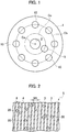
- the regions in which the detection target substances 11 and the nanoparticles 20 are captured are the reaction regions 10 shown in Fig. 1 . While Fig. 1 illustrates eight reaction regions 10 arranged at regular intervals such that the respective center points are located on the common circle Cb concentric with the analysis substrate 1 having the center Ca, the number and positions of the reaction regions 10 formed are not limited to this illustration.
- a configuration of an analysis device of detecting the nanoparticles 20 captured in the reaction regions 10 of the analysis substrate 1 is illustrated below with reference to Fig. 4 .
- the analysis device 1 includes a turntable 31, a clamper 32, a turntable drive unit 33, a turntable drive circuit 34, a guide shaft 35, an optical pickup 40, an optical pickup drive circuit 36, and a controller 37.
- the analysis substrate 1 is placed on the turntable 31 with the reaction regions 10 facing down.
- the clamper 32 is driven in directions separating from and approaching the turntable 31, namely, in the upper and lower directions in Fig. 4 .
- the analysis substrate 1 is held between the turntable 31 and the clamper 32 when the clamper 32 is driven downward.
- the analysis substrate 1 is held such that the center Ca is located on a rotation axis C31 of the turntable 31.
- the turntable drive unit 33 drives the turntable 31 to rotate on the rotation axis C31 together with the analysis substrate 1 and the clamper 32.
- a spindle motor may be used as the turntable drive unit 33.
- the turntable drive circuit 34 controls the turntable drive unit 33.
- the turntable drive circuit 34 controls the turntable drive unit 33 such that the turntable 31 rotates at a constant linear velocity Lv together with the analysis substrate 1 and the clamper 32.
- the guide shaft 35 is placed in parallel to the analysis substrate 1 in the radial direction of the analysis substrate 1.
- the guide shaft 35 is arranged in a direction perpendicular to the rotation axis C31 of the turntable 31.
- the optical pickup 40 is supported by the guide shaft 35.
- the optical pickup 40 is driven along the guide shaft 35 in the radial direction of the analysis substrate 1 and in parallel to the analysis substrate 1.
- the optical pickup 40 is driven in a direction perpendicular to the rotation axis C31 of the turntable 31.
- the optical pickup 40 includes an objective lens 41.
- the objective lens 41 is supported by suspension wires 42.
- the objective lens 41 is driven in the directions separating from and approaching the analysis substrate 1, namely, in the upper and lower directions in Fig. 4 .
- the optical pickup 40 emits laser light 40a to the analysis substrate 1.
- the laser light 40a is condensed by the objective lens 41 on the surface of the analysis substrate 1 provided with the reaction regions 10 (on the lower surface of the analysis substrate 1 in Fig. 4 ).
- the laser light 40a has a wavelength ⁇ of 405 nm, for example.
- the optical pickup 40 receives the reflected light from the analysis substrate 1.
- the optical pickup 40 detects a light reception level of the reflected light, generates a light reception level signal JS, and outputs the signal to the controller 37.
- the optical pickup drive circuit 36 controls the operation of the optical pickup 40.
- the optical pickup drive circuit 36 moves the optical pickup 40 along the guide shaft 35 or moves the objective lens 41 of the optical pickup 40 in the vertical direction, for example.
- the controller 37 controls the turntable drive circuit 34 and the optical pickup drive circuit 36.
- a central processing unit CPU may be used as the controller 37, for example.
- the controller 37 includes a signal detector 50 for detecting signals from the analysis substrate 1.
- the signal detector 50 includes a substrate level detection circuit 51, a memory circuit 52, a light reception signal detection circuit 53, a determination circuit 54, and a counter circuit 55.
- the signal detector 50 extracts and counts the nanoparticle detection signals KS from the light reception level signal JS output from the optical pickup 40, so as to detect and quantitate the nanoparticles 20 captured in the reaction regions 10. It is difficult to directly detect the detection target substances 11, since the detection target substances 11 have a size as small as 100 nm.
- the present embodiment detects and quantitates the nanoparticles 20 having a greater size than the detection target substances 11 so as to indirectly detect and quantitate the detection target substances 11 captured in the reaction regions 10.
- step S1 the controller 37 controls the turntable drive circuit 34 to direct the turntable drive unit 33 to drive the turntable 31 so that the analysis substrate 1 provided with the reaction regions 10 rotates at a constant linear velocity Lv.
- step S2 the substrate level detection circuit 51 directs the optical pickup 40 to emit the laser light 40a to the analysis substrate 1, and controls the optical pickup drive circuit 36 to move the optical pickup 40 to a radial position of a predetermined non-reaction region 9 in the analysis substrate 1 at which the reaction region 10 is not formed.
- step S3 the optical pickup 40 receives the reflected light from the non-reaction region 9.
- the optical pickup 40 detects a light reception level of the reflected light from the non-reaction region 9, generates a light reception level signal JS, and outputs the signal to the substrate level detection circuit 51.
- step S4 the substrate level detection circuit 51 extracts a light reception level of the light reception level signal JS of the non-reaction region 9 as a substrate signal level DL, and stores the extracted level in the memory circuit 52.
- the substrate signal level DL depends on the substrate characteristics of the analysis substrate 1.
- the processing from step S2 to step S4 for extracting the substrate signal level DL does not need to be repeated every time the analysis substrate 1 is replaced when the analysis substrates 1 having the same design are used.
- the extraction of the substrate signal level DL may be performed only once during the operation of the analysis device 30, or may be repeated every time the lot of the analysis substrates 1 is changed to a new lot.
- step S2 When the extraction of the substrate signal level DL is the first step, the processing from step S2 to step S4 may be omitted.
- the present embodiment exemplifies a case in which the light reception level signal JS from the non-reaction region 9 is obtained every time the analysis substrate 1 is replaced.
- step S5 the light reception signal detection circuit 53 directs the optical pickup 40 to emit the laser light 40a to the analysis substrate 1, and controls the optical pickup drive circuit 36 to move the optical pickup 40 to a radial position in the analysis substrate 1 at which the reaction region 10 is formed. As shown in Fig. 3 , the reaction region 10 is irradiated with the laser light 40a and scanned along the recesses 4.
- step S6 the optical pickup 40 receives the reflected light from the reaction region 10.
- the optical pickup 40 detects the light reception level of the reflected light, generates a light reception level signal JS, and outputs the signal to the light reception signal detection circuit 53.
- Fig. 6 is a graph showing an example of the light reception level signal JS obtained by the analysis method according to the present embodiment.
- the vertical axis in Fig. 6 represents a signal level of the light reception level signal JS, and the horizontal axis represents a time.
- the light reception level of the reflected light from the reaction region 10, which is the reflected light from the analysis substrate 1 is referred to as a substrate signal level DL.
- the substrate signal level DL is in particular a light reception level of the reflected light from a recess 4 in the reaction region 10 of the analysis substrate 1.
- a light reception level signal having a signal level (a high level) higher than the substrate signal level DL is a nanoparticle detection signal KS
- a light reception level signal having a signal level (a low level) lower than the substrate signal level DL is a noise signal NS.
- the substrate signal level DL in the light reception level signal JS is a constant light reception level during a period not including either the nanoparticle detection signal KS or the noise signal NS.
- reaction regions 10 During the process of forming the reaction regions 10, more particularly, in the steps of capturing the detection target substances 11 on the analysis substrate 1 by an antigen-antibody reaction, and washing out unreacted and unnecessary substances, an aggregation of proteins, salt contained in a cleaning liquid, or a surfactant may remain as residues in the reaction regions 10.
- the noise signal NS derived from such residues is also detected as the light reception level signal JS.
- Fig. 8 is a partly-enlarged view of Fig. 7 .
- the vertical axis in each of Fig. 7 and Fig. 8 represents a signal level (a voltage relative value) of the nanoparticle detection signal KS, and the horizontal axis represents a refractive index n of a real part in the complex refractive index m of the nanoparticles.
- ki is an imaginary part
- k is an extinction coefficient.
- DL is a substrate signal level.
- Fig. 9 is a graph showing a relationship between conventional nanoparticle detection signals KS and noise signals NS.
- nanoparticles are made of synthetic resin such as polystyrene.
- Typical synthetic resin such as polystyrene has a refractive index n of about 1.5 and an extinction coefficient k of about 0.2 to 0.4.
- the nanoparticle detection signals KS have signal levels lower than the substrate signal level DL, as shown in Fig. 9 .
- the nanoparticle detection signals KS and the noise signals NS are thus detected as signal levels lower than the substrate signal level DL, as shown in Fig. 9 .
- Nanoparticle detection signals KS typically have lower signal levels than noise signals NS. It is thus possible to distinguish between the nanoparticle detection signals KS and the noise signals NS with some accuracy by comparing the respective signal levels of the light reception level signals with a threshold Ltha. However, if the amount of nanoparticles detected is quite small, an influence of the noise signals NS is relatively increased, decreasing the accuracy of quantitating nanoparticles.
- the present embodiment uses the nanoparticles 20 of which the nanoparticle detection signals KS have higher signal levels than the substrate signal level DL.
- Such material may be a metal compound including an oxide of transition metal such as titanium oxide, niobium oxide, and tantalum oxide.
- the surfaces of the nanoparticles 20 may be polymerized and covered with resin material in order to provide a ligand.
- the effective complex refractive index of the nanoparticles 20 thus leads to a synthetic complex refractive index of the metal compound and the resin material.
- the polymerization covering of the surfaces of the nanoparticles 20 with such a thin resin film can provide a ligand.
- the nanoparticle detection signals KS can have higher signal levels than the substrate signal level DL when a refractive index n and an extinction coefficient k of the synthetic complex refractive index are set to the same ranges as described above.
- a magnetic substance may be enclosed in the nanoparticles 20 in order to magnetically capture the nanoparticles 20.
- the effective complex refractive index of the nanoparticles 20 thus leads to a synthetic complex refractive index of the metal compound and the magnetic substance.
- the nanoparticle detection signals KS can have higher signal levels than the substrate signal level DL when a refractive index n and an extinction coefficient k of the synthetic complex refractive index are set to the same ranges as described above.
- the reaction regions 10 are irradiated with the laser light 40a and scanned along the recesses 4.
- the nanoparticles 20 are preferably captured in the recesses 4 along the scanning direction with a high probability so as to quantitate the nanoparticles 20 accurately. If a diameter d of the nanoparticles 20 (refer to Fig. 3 ) is smaller than ⁇ /4, the accuracy of detecting the nanoparticles 20 may be decreased, or some nanoparticles 20 may be captured and aligned in the direction orthogonal to the scanning direction to decrease the accuracy of quantitating the nanoparticles 20.
- the symbol " ⁇ " represents a wavelength of the laser light 40a emitted to the nanoparticles 20.
- the diameter d of the nanoparticles 20 is therefore preferably in a range of ⁇ /4 to ⁇ /2 ( ⁇ /4 ⁇ d ⁇ ⁇ /2).
- the determination circuit 54 determines that a light reception level signal with a signal level higher than the substrate signal level DL stored in the memory circuit 52 is the nanoparticle detection signal KS. For example, the determination circuit 54 compares the light reception level signal JS with a threshold Lth, and determines that the light reception level signal JS having the signal level greater than or equal to the threshold Lth is the nanoparticle detection signal KS.
- the threshold Lth is set to be a higher level than the substrate signal level DL.
- the noise signals NS included in the light reception level signal JS can easily be distinguished from the nanoparticle detection signals KS, since the nanoparticle detection signals KS have higher signal levels than the substrate signal level DL and the noise signals NS have lower signal levels than the substrate signal level DL. Accordingly, only the nanoparticle detection signals KS can be extracted from the light reception level signal JS accurately.
- step S8 the counter circuit 55 counts the nanoparticle detection signals KS, in particular, the number of pulses of the nanoparticle detection signals KS for each reaction region 10, and sums up the counted values per track.
- the counter circuit 55 thus can quantitate the nanoparticles 20 in the reaction regions 10.
- the quantitation of the nanoparticles 20 leads to indirect quantitation of the detection target substances 11 labeled by the nanoparticles 20.
- step S9 the controller 37 controls the optical pickup drive circuit 36 to move the optical pickup 40 to the initial position, and stops the irradiation of the laser light 40a.
- the controller 37 then controls the turntable drive circuit 34 to stop the rotation of the turntable 31.
- the analysis method according to the present embodiment uses the nanoparticles 20 of which the nanoparticle detection signals KS have higher signal levels than the substrate signal level DL, so as to facilitate the distinction of the nanoparticle detection signals KS from noise signals having lower signal levels than the substrate signal level DL.
- the light reception level signal JS is compared with the threshold Lth set to a higher level than the substrate signal level DL, so as to accurately extract only the nanoparticle detection signals KS from the light reception level signal JS. Accordingly, the nanoparticles 20 captured in the reaction regions 10 can be detected accurately in accordance with the nanoparticle detection signals KS extracted.
- the analysis method according to the present embodiment can extract nanoparticle detection signals with a higher accuracy than conventional methods to detect nanoparticles based on the extracted nanoparticle detection signals, so as to improve the accuracy of indirectly detecting detection target substances.
- the present invention can be utilized for analyzing biomaterials such as antigens and antibodies.
Landscapes
- Health & Medical Sciences (AREA)
- Life Sciences & Earth Sciences (AREA)
- Chemical & Material Sciences (AREA)
- Immunology (AREA)
- Engineering & Computer Science (AREA)
- Biomedical Technology (AREA)
- Urology & Nephrology (AREA)
- Molecular Biology (AREA)
- Hematology (AREA)
- General Health & Medical Sciences (AREA)
- General Physics & Mathematics (AREA)
- Pathology (AREA)
- Biochemistry (AREA)
- Analytical Chemistry (AREA)
- Physics & Mathematics (AREA)
- Medicinal Chemistry (AREA)
- Food Science & Technology (AREA)
- Biotechnology (AREA)
- Microbiology (AREA)
- Cell Biology (AREA)
- Nanotechnology (AREA)
- Inorganic Chemistry (AREA)
- Dispersion Chemistry (AREA)
- Investigating Or Analysing Materials By Optical Means (AREA)
Abstract
Description
- The present disclosure relates to an analysis method and an analysis device of analyzing biomaterials such as antigens and antibodies.
- Immunoassays are known to quantitatively analyze disease detection and therapeutic effects by detecting particular antigens or antibodies as biomarkers associated with diseases.
-
Patent Literature 1 discloses an analysis method and an analysis device in which antibodies that are fixed to a reaction region on an analysis substrate are allowed to bind to antigens that are detection target substances in a specimen, and the detection target substances further bound to nanoparticles are captured on the reaction region and scanned with laser light emitted from an optical pickup, so as to detect the nanoparticles captured on the reaction region. - The conventional analysis method as disclosed in
Patent Literature 1 scans the reaction region by emitting the laser light from the optical pickup, and analyzes the reflected light from the reaction region to detect the nanoparticles, so as to detect the detection target substances indirectly. The analysis method and the analysis device disclosed inPatent Literature 1 are the application of an optical disc and an optical disc device to specimen detection. - Patent Literature 1: Japanese Translation of
PCT International Application Publication No. 2002-530786 - During the process of forming the reaction region, more particularly, in the steps of capturing the detection target substances on the analysis substrate by an antigen-antibody reaction, and washing out unreacted and unnecessary substances, an aggregation of proteins, salt contained in a cleaning liquid, or a surfactant may remain as residues in the reaction region. The residues are detected when the nanoparticles are detected.
- Detection signals (noise signals) derived from residues and detection signals (nanoparticle detection signals) derived from nanoparticles typically have similar pulse waveforms. The conventional analysis method and analysis device cannot distinguish between the noise signals and the nanoparticle detection signals with a high accuracy. When the amount of detection target substances contained is quite small, nanoparticles binding to the detection target substances and captured on the reaction region are decreased to a quite small amount. As a result, influence of the noise signals is relatively increased, and accuracy of quantitatively analyzing the nanoparticles is decreased, which particularly leads to limitations on accurate detection of the nanoparticles, or a decrease in the accuracy of quantitation analysis of decomposition of the nanoparticles.
- An object of an embodiment is to provide an analysis method and an analysis device capable of extracting nanoparticle detection signals with a higher accuracy than conventional methods and devices to detect nanoparticles based on the extracted nanoparticle detection signals, so as to improve the accuracy of indirectly detecting detection target substances.
- A first aspect of the embodiment provides an analysis method including: irradiating, with laser light, an analysis substrate made of a resin material and having a reaction region on which detection target substances and nanoparticles of a metal compound for labeling the detection target substances are captured; extracting, as a substrate signal level, a signal level generated when receiving reflected light from the analysis substrate; receiving reflected light from the reaction region to generate a light reception level signal; extracting a nanoparticle detection signal having a higher signal level than the substrate signal level from the light reception level signal of the reflected light from the reaction region; and detecting the nanoparticles in accordance with the extracted nanoparticle detection signal.
- A second aspect of the embodiment provides an analysis device including: an optical pickup configured to irradiate, with laser light, an analysis substrate made of a resin material and having a reaction region on which detection target substances and nanoparticles of a metal compound for labeling the detection target substance are captured, and to detect light reception levels of reflected light from the reaction region and a non-reaction region at which the reaction region is not formed so as to generate light reception level signals; a substrate level detection circuit configured to extract, as a substrate signal level, a signal level of a light reception level signal from the non-reaction region; a determination circuit configured to extract a nanoparticle detection signal having a higher signal level than the substrate signal level from the light reception level signal of the reflected light from the reaction region; and a counter circuit configured to detect the nanoparticles in accordance with the nanoparticle detection signal.
- The analysis method and the analysis device according to the embodiment can extract nanoparticle detection signals with a higher accuracy than conventional methods and devices to detect nanoparticles based on the extracted nanoparticle detection signals, so as to improve the accuracy of indirectly detecting detection target substances.
-
-
Fig. 1 is a top view of an analysis substrate provided with reaction regions. -
Fig. 2 is an enlarged schematic view illustrating a state in which nanoparticles are captured on a track region of a reaction region. -
Fig. 3 is an enlarged schematic view illustrating a state in which nanoparticles specifically binding to detection target substances are captured on a track region of a reaction region. -
Fig. 4 is a configuration diagram showing an analysis device according to the embodiment. -
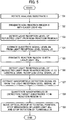
Fig. 5 is a flowchart for describing a method of analyzing nanoparticles according to the embodiment. -
Fig. 6 is a graph illustrating a light reception level signal obtained by the analysis method according to the embodiment. -
Fig. 7 is a graph showing a relationship between a complex refractive index of nanoparticles and a signal level of a light reception level signal obtained by a simulation. -
Fig. 8 is a partly-enlarged view ofFig. 7 . -
Fig. 9 is a graph illustrating a conventional light reception level signal. - A method of forming reaction regions on an analysis substrate is described below with reference to
Fig. 1 to Fig. 3 . - As shown in
Fig. 1 , ananalysis substrate 1 is formed into a circular shape having substantially the same dimensions as optical discs such as Blu-ray discs (BDs), DVDs, and compact discs (CDs). Theanalysis substrate 1 is provided with apositioning hole 2 in the middle. - The
analysis substrate 1 is formed of resin material such as polycarbonate resin and cycloolefin polymer, commonly used for optical discs. Theanalysis substrate 1 is not limited to the optical discs described above, and may be any optical disc according to other embodiments or conforming to prescribed standards. - As shown in
Fig. 2 , the surface of theanalysis substrate 1 includestrack regions 5 provided withconvex regions 3 andrecesses 4 alternately arranged in a radial direction. Theconvex regions 3 and therecesses 4 are formed in a spiral from the inner side to the outer side of theanalysis substrate 1. A track pitch W4 of the recesses 4 (the convex regions 3) in the radial direction is 320 nanometers (nm), for example. - The
track regions 5 of theanalysis substrate 1 are provided withreaction regions 10. The method of forming thereaction regions 10 is described below with reference toFig. 3 . -
Antibodies 12, which specifically bind todetection target substances 11 as particular antigens associated with a disease, are fixed to predetermined regions (in which thereaction regions 10 are formed) on thetrack regions 5. For example, a buffer solution including theantibodies 12 is reacted with theanalysis substrate 1. The buffer solution after the reaction is then removed, and theanalysis substrate 1 is washed and dried, so as to fix theantibodies 12 to thetrack regions 5. Thedetection target substances 11 are specific proteins, for example. - The
detection target substances 11 are specifically bound to theantibodies 12 fixed to thetrack regions 5. For example, a sample solution, including thedetection target substances 11, is reacted with theantibodies 12. The sample solution after the reaction is then removed, and theanalysis substrate 1 is washed and dried, so as to capture thedetection target substances 11 on therecesses 4 of thereaction regions 5. An outer diameter of thedetection target substances 11 is 100 nm, for example. Sample solutions sometimes do not include thedetection target substances 11. The following is a case in which the sample solution includes thedetection target substances 11 for illustration purposes. -
Nanoparticles 20 for labeling thedetection target substances 11 specifically bind to thedetection target substances 11 captured on thetrack regions 5. The surfaces of thenanoparticles 20 are provided withantibodies 21 specifically binding to thedetection target substances 11. When theantibodies 21 of thenanoparticles 20 specifically bind to thedetection target substances 11, thenanoparticles 20 are captured in therecesses 4 of thetrack regions 5. The size and material characteristics of thenanoparticles 20 are described below. - The detection target
substances 11 and thenanoparticles 20 are thus captured in therecesses 4 of thetrack regions 5 of theanalysis substrate 1. The regions in which the detection targetsubstances 11 and thenanoparticles 20 are captured are thereaction regions 10 shown inFig. 1 . WhileFig. 1 illustrates eightreaction regions 10 arranged at regular intervals such that the respective center points are located on the common circle Cb concentric with theanalysis substrate 1 having the center Ca, the number and positions of thereaction regions 10 formed are not limited to this illustration. - A configuration of an analysis device of detecting the
nanoparticles 20 captured in thereaction regions 10 of theanalysis substrate 1 is illustrated below with reference toFig. 4 . - The
analysis device 1 includes aturntable 31, aclamper 32, aturntable drive unit 33, aturntable drive circuit 34, aguide shaft 35, anoptical pickup 40, an opticalpickup drive circuit 36, and acontroller 37. - The
analysis substrate 1 is placed on theturntable 31 with thereaction regions 10 facing down. - The
clamper 32 is driven in directions separating from and approaching theturntable 31, namely, in the upper and lower directions inFig. 4 . Theanalysis substrate 1 is held between theturntable 31 and theclamper 32 when theclamper 32 is driven downward. In particular, theanalysis substrate 1 is held such that the center Ca is located on a rotation axis C31 of theturntable 31. - The
turntable drive unit 33 drives theturntable 31 to rotate on the rotation axis C31 together with theanalysis substrate 1 and theclamper 32. A spindle motor may be used as theturntable drive unit 33. - The
turntable drive circuit 34 controls theturntable drive unit 33. For example, theturntable drive circuit 34 controls theturntable drive unit 33 such that theturntable 31 rotates at a constant linear velocity Lv together with theanalysis substrate 1 and theclamper 32. - The
guide shaft 35 is placed in parallel to theanalysis substrate 1 in the radial direction of theanalysis substrate 1. Theguide shaft 35 is arranged in a direction perpendicular to the rotation axis C31 of theturntable 31. - The
optical pickup 40 is supported by theguide shaft 35. Theoptical pickup 40 is driven along theguide shaft 35 in the radial direction of theanalysis substrate 1 and in parallel to theanalysis substrate 1. Theoptical pickup 40 is driven in a direction perpendicular to the rotation axis C31 of theturntable 31. - The
optical pickup 40 includes anobjective lens 41. Theobjective lens 41 is supported bysuspension wires 42. Theobjective lens 41 is driven in the directions separating from and approaching theanalysis substrate 1, namely, in the upper and lower directions inFig. 4 . - The
optical pickup 40 emitslaser light 40a to theanalysis substrate 1. Thelaser light 40a is condensed by theobjective lens 41 on the surface of theanalysis substrate 1 provided with the reaction regions 10 (on the lower surface of theanalysis substrate 1 inFig. 4 ). Thelaser light 40a has a wavelength λ of 405 nm, for example. - The
optical pickup 40 receives the reflected light from theanalysis substrate 1. Theoptical pickup 40 detects a light reception level of the reflected light, generates a light reception level signal JS, and outputs the signal to thecontroller 37. - The optical
pickup drive circuit 36 controls the operation of theoptical pickup 40. The opticalpickup drive circuit 36 moves theoptical pickup 40 along theguide shaft 35 or moves theobjective lens 41 of theoptical pickup 40 in the vertical direction, for example. - The
controller 37 controls theturntable drive circuit 34 and the opticalpickup drive circuit 36. A central processing unit (CPU) may be used as thecontroller 37, for example. - The
controller 37 includes asignal detector 50 for detecting signals from theanalysis substrate 1. Thesignal detector 50 includes a substratelevel detection circuit 51, amemory circuit 52, a light receptionsignal detection circuit 53, adetermination circuit 54, and acounter circuit 55. - The
signal detector 50 extracts and counts the nanoparticle detection signals KS from the light reception level signal JS output from theoptical pickup 40, so as to detect and quantitate thenanoparticles 20 captured in thereaction regions 10. It is difficult to directly detect thedetection target substances 11, since thedetection target substances 11 have a size as small as 100 nm. The present embodiment detects and quantitates thenanoparticles 20 having a greater size than thedetection target substances 11 so as to indirectly detect and quantitate thedetection target substances 11 captured in thereaction regions 10. - An analysis method of analyzing the nanoparticles 20 (the detection target substances 11) is described below with reference to the flowchart shown in
Fig. 5 . When a sample solution does not include thedetection target substances 11, nodetection target substance 11 ornanoparticle 20 is captured in thereaction regions 10 of theanalysis substrate 1. The following is a case in which thedetection target substances 11 and thenanoparticles 20 are captured in thereaction regions 10 for illustration purposes. - In step S1, the
controller 37 controls theturntable drive circuit 34 to direct theturntable drive unit 33 to drive theturntable 31 so that theanalysis substrate 1 provided with thereaction regions 10 rotates at a constant linear velocity Lv. - In step S2, the substrate
level detection circuit 51 directs theoptical pickup 40 to emit thelaser light 40a to theanalysis substrate 1, and controls the opticalpickup drive circuit 36 to move theoptical pickup 40 to a radial position of apredetermined non-reaction region 9 in theanalysis substrate 1 at which thereaction region 10 is not formed. Thenon-reaction region 9 located on a circle Cc concentric with theanalysis substrate 1 having the center Ca where thereaction region 10 is not provided as shown inFig. 1 , for example, is irradiated with thelaser light 40a and scanned. - In step S3, the
optical pickup 40 receives the reflected light from thenon-reaction region 9. Theoptical pickup 40 detects a light reception level of the reflected light from thenon-reaction region 9, generates a light reception level signal JS, and outputs the signal to the substratelevel detection circuit 51. - In step S4, the substrate
level detection circuit 51 extracts a light reception level of the light reception level signal JS of thenon-reaction region 9 as a substrate signal level DL, and stores the extracted level in thememory circuit 52. - The substrate signal level DL depends on the substrate characteristics of the
analysis substrate 1. The processing from step S2 to step S4 for extracting the substrate signal level DL does not need to be repeated every time theanalysis substrate 1 is replaced when theanalysis substrates 1 having the same design are used. The extraction of the substrate signal level DL may be performed only once during the operation of theanalysis device 30, or may be repeated every time the lot of theanalysis substrates 1 is changed to a new lot. - When the extraction of the substrate signal level DL is the first step, the processing from step S2 to step S4 may be omitted. The present embodiment exemplifies a case in which the light reception level signal JS from the
non-reaction region 9 is obtained every time theanalysis substrate 1 is replaced. - In step S5, the light reception
signal detection circuit 53 directs theoptical pickup 40 to emit thelaser light 40a to theanalysis substrate 1, and controls the opticalpickup drive circuit 36 to move theoptical pickup 40 to a radial position in theanalysis substrate 1 at which thereaction region 10 is formed. As shown inFig. 3 , thereaction region 10 is irradiated with thelaser light 40a and scanned along therecesses 4. - In step S6, the
optical pickup 40 receives the reflected light from thereaction region 10. Theoptical pickup 40 detects the light reception level of the reflected light, generates a light reception level signal JS, and outputs the signal to the light receptionsignal detection circuit 53. -
Fig. 6 is a graph showing an example of the light reception level signal JS obtained by the analysis method according to the present embodiment. The vertical axis inFig. 6 represents a signal level of the light reception level signal JS, and the horizontal axis represents a time. The light reception level of the reflected light from thereaction region 10, which is the reflected light from theanalysis substrate 1, is referred to as a substrate signal level DL. The substrate signal level DL is in particular a light reception level of the reflected light from arecess 4 in thereaction region 10 of theanalysis substrate 1. - A light reception level signal having a signal level (a high level) higher than the substrate signal level DL is a nanoparticle detection signal KS, and a light reception level signal having a signal level (a low level) lower than the substrate signal level DL is a noise signal NS. The substrate signal level DL in the light reception level signal JS is a constant light reception level during a period not including either the nanoparticle detection signal KS or the noise signal NS.
- During the process of forming the
reaction regions 10, more particularly, in the steps of capturing thedetection target substances 11 on theanalysis substrate 1 by an antigen-antibody reaction, and washing out unreacted and unnecessary substances, an aggregation of proteins, salt contained in a cleaning liquid, or a surfactant may remain as residues in thereaction regions 10. The noise signal NS derived from such residues is also detected as the light reception level signal JS. -
Fig. 7 is a graph showing a relationship between a complex refractive index m (m = n - ki) of nanoparticles and a signal level of a nanoparticle detection signal KS, obtained by an optical simulation by a finite-difference time-domain (FDTD) method.Fig. 8 is a partly-enlarged view ofFig. 7 . - The vertical axis in each of
Fig. 7 andFig. 8 represents a signal level (a voltage relative value) of the nanoparticle detection signal KS, and the horizontal axis represents a refractive index n of a real part in the complex refractive index m of the nanoparticles. In the complex refractive index (m = n - ki), ki is an imaginary part, and k is an extinction coefficient. InFig. 7 andFig. 8 , Lk0, Lk1, Lk2, Lk3, and Lk4 are signal levels of nanoparticle detection signals KS when k = 0, k = 0.1, k = 0.2, k = 0.3, and k = 0.4, and DL is a substrate signal level.Fig. 7 andFig. 8 each show a result of the optical simulation under the conditions that thelaser light 40a has a wavelength λ of 405 nm, the outer diameter of the nanoparticles is 200 nm, and the refractive index n of the real part in theanalysis substrate 1 is 1.53 (ki = 0). -
Fig. 9 is a graph showing a relationship between conventional nanoparticle detection signals KS and noise signals NS. Conventionally, nanoparticles are made of synthetic resin such as polystyrene. Typical synthetic resin such as polystyrene has a refractive index n of about 1.5 and an extinction coefficient k of about 0.2 to 0.4. In the conventional case, the nanoparticle detection signals KS have signal levels lower than the substrate signal level DL, as shown inFig. 9 . The nanoparticle detection signals KS and the noise signals NS are thus detected as signal levels lower than the substrate signal level DL, as shown inFig. 9 . - Nanoparticle detection signals KS typically have lower signal levels than noise signals NS. It is thus possible to distinguish between the nanoparticle detection signals KS and the noise signals NS with some accuracy by comparing the respective signal levels of the light reception level signals with a threshold Ltha. However, if the amount of nanoparticles detected is quite small, an influence of the noise signals NS is relatively increased, decreasing the accuracy of quantitating nanoparticles.
- The present embodiment uses the
nanoparticles 20 of which the nanoparticle detection signals KS have higher signal levels than the substrate signal level DL. In particular, thenanoparticles 20 are made of material having a complex refractive index (m = n - ki), where an extinction coefficient k of an imaginary part is 0.3 or smaller (k ≤ 0.3) and a refractive index n of a real part is in a range of 2.1 to 2.5 (2.1 ≤ n ≤ 2.5), or where an extinction coefficient k of an imaginary part is 0.2 or smaller (k ≤ 0.2) and a refractive index n of a real part is in a range of 2.1 to 2.6 (2.1 ≤ n ≤ 2.6). Such material may be a metal compound including an oxide of transition metal such as titanium oxide, niobium oxide, and tantalum oxide. - The surfaces of the
nanoparticles 20 may be polymerized and covered with resin material in order to provide a ligand. The effective complex refractive index of thenanoparticles 20 thus leads to a synthetic complex refractive index of the metal compound and the resin material. The polymerization covering of the surfaces of thenanoparticles 20 with such a thin resin film can provide a ligand. The nanoparticle detection signals KS can have higher signal levels than the substrate signal level DL when a refractive index n and an extinction coefficient k of the synthetic complex refractive index are set to the same ranges as described above. - A magnetic substance may be enclosed in the
nanoparticles 20 in order to magnetically capture thenanoparticles 20. The effective complex refractive index of thenanoparticles 20 thus leads to a synthetic complex refractive index of the metal compound and the magnetic substance. The nanoparticle detection signals KS can have higher signal levels than the substrate signal level DL when a refractive index n and an extinction coefficient k of the synthetic complex refractive index are set to the same ranges as described above. - The
reaction regions 10 are irradiated with thelaser light 40a and scanned along therecesses 4. Thenanoparticles 20 are preferably captured in therecesses 4 along the scanning direction with a high probability so as to quantitate thenanoparticles 20 accurately. If a diameter d of the nanoparticles 20 (refer toFig. 3 ) is smaller than λ/4, the accuracy of detecting thenanoparticles 20 may be decreased, or somenanoparticles 20 may be captured and aligned in the direction orthogonal to the scanning direction to decrease the accuracy of quantitating thenanoparticles 20. The symbol "λ" represents a wavelength of thelaser light 40a emitted to thenanoparticles 20. - If the diameter d of the
nanoparticles 20 is greater than λ/2, the amount of thenanoparticles 20 captured in therecesses 4 is decreased. The diameter d of thenanoparticles 20 is therefore preferably in a range of λ/4 to λ/2 (λ/4 ≤ d ≤ λ/2). - Returning to
Fig. 5 , in step S7, thedetermination circuit 54 determines that a light reception level signal with a signal level higher than the substrate signal level DL stored in thememory circuit 52 is the nanoparticle detection signal KS. For example, thedetermination circuit 54 compares the light reception level signal JS with a threshold Lth, and determines that the light reception level signal JS having the signal level greater than or equal to the threshold Lth is the nanoparticle detection signal KS. The threshold Lth is set to be a higher level than the substrate signal level DL. - The noise signals NS included in the light reception level signal JS can easily be distinguished from the nanoparticle detection signals KS, since the nanoparticle detection signals KS have higher signal levels than the substrate signal level DL and the noise signals NS have lower signal levels than the substrate signal level DL. Accordingly, only the nanoparticle detection signals KS can be extracted from the light reception level signal JS accurately.
- In step S8, the
counter circuit 55 counts the nanoparticle detection signals KS, in particular, the number of pulses of the nanoparticle detection signals KS for eachreaction region 10, and sums up the counted values per track. Thecounter circuit 55 thus can quantitate thenanoparticles 20 in thereaction regions 10. The quantitation of thenanoparticles 20 leads to indirect quantitation of thedetection target substances 11 labeled by thenanoparticles 20. - In step S9, the
controller 37 controls the opticalpickup drive circuit 36 to move theoptical pickup 40 to the initial position, and stops the irradiation of thelaser light 40a. Thecontroller 37 then controls theturntable drive circuit 34 to stop the rotation of theturntable 31. - The analysis method according to the present embodiment uses the
nanoparticles 20 of which the nanoparticle detection signals KS have higher signal levels than the substrate signal level DL, so as to facilitate the distinction of the nanoparticle detection signals KS from noise signals having lower signal levels than the substrate signal level DL. For example, the light reception level signal JS is compared with the threshold Lth set to a higher level than the substrate signal level DL, so as to accurately extract only the nanoparticle detection signals KS from the light reception level signal JS. Accordingly, thenanoparticles 20 captured in thereaction regions 10 can be detected accurately in accordance with the nanoparticle detection signals KS extracted. - The analysis method according to the present embodiment can extract nanoparticle detection signals with a higher accuracy than conventional methods to detect nanoparticles based on the extracted nanoparticle detection signals, so as to improve the accuracy of indirectly detecting detection target substances.
- It should be understood that the present invention is not intended to be limited to the embodiment described above, and various modifications will be apparent to those skilled in the art without departing from the scope of the present invention.
- The present invention can be utilized for analyzing biomaterials such as antigens and antibodies.
Claims (5)
- An analysis method comprising:irradiating, with laser light, an analysis substrate made of a resin material and having a reaction region on which detection target substances and nanoparticles of a metal compound for labeling the detection target substances are captured;extracting, as a substrate signal level, a signal level generated when receiving reflected light from the analysis substrate;receiving reflected light from the reaction region to generate a light reception level signal;extracting a nanoparticle detection signal having a higher signal level than the substrate signal level from the light reception level signal of the reflected light from the reaction region; anddetecting the nanoparticles in accordance with the extracted nanoparticle detection signal.
- The analysis method according to claim 1, wherein the nanoparticles have a complex refractive index n - ki, where an extinction coefficient k of an imaginary part ki is 0.3 or smaller and a refractive index n of a real part is in a range of 2.1 to 2.5, or where an extinction coefficient k of an imaginary part ki is 0.2 or smaller and a refractive index n of a real part is in a range of 2.1 to 2.6.
- The analysis method according to claim 1 or 2, wherein the nanoparticles are covered with a resin film.
- The analysis method according to claim 1 or 2, wherein a magnetic body is enclosed in the nanoparticles.
- An analysis device comprising:an optical pickup configured to irradiate, with laser light, an analysis substrate made of a resin material and having a reaction region on which detection target substances and nanoparticles of a metal compound for labeling the detection target substance are captured, and to detect light reception levels of reflected light from the reaction region and a non-reaction region not provided with the reaction region so as to generate light reception level signals;a substrate level detection circuit configured to extract, as a substrate signal level, a signal level of a light reception level signal from the non-reaction region;a determination circuit configured to extract a nanoparticle detection signal having a higher signal level than the substrate signal level from the light reception level signal of the reflected light from the reaction region; anda counter circuit configured to detect the nanoparticles in accordance with the nanoparticle detection signal.
Applications Claiming Priority (2)
| Application Number | Priority Date | Filing Date | Title |
|---|---|---|---|
| JP2016097830A JP6740703B2 (en) | 2016-05-16 | 2016-05-16 | Analysis method and analyzer |
| PCT/JP2017/016894 WO2017199731A1 (en) | 2016-05-16 | 2017-04-28 | Analysis method and analyzing device |
Publications (3)
| Publication Number | Publication Date |
|---|---|
| EP3460473A1 true EP3460473A1 (en) | 2019-03-27 |
| EP3460473A4 EP3460473A4 (en) | 2019-03-27 |
| EP3460473B1 EP3460473B1 (en) | 2020-12-09 |
Family
ID=60325085
Family Applications (1)
| Application Number | Title | Priority Date | Filing Date |
|---|---|---|---|
| EP17799161.9A Not-in-force EP3460473B1 (en) | 2016-05-16 | 2017-04-28 | Analysis method and analysis device |
Country Status (5)
| Country | Link |
|---|---|
| US (1) | US10520417B2 (en) |
| EP (1) | EP3460473B1 (en) |
| JP (1) | JP6740703B2 (en) |
| CN (1) | CN109154608B (en) |
| WO (1) | WO2017199731A1 (en) |
Families Citing this family (7)
| Publication number | Priority date | Publication date | Assignee | Title |
|---|---|---|---|---|
| JP7208468B2 (en) * | 2018-08-01 | 2023-01-19 | 株式会社Jvcケンウッド | Analysis device and analysis method |
| CN109243660B (en) * | 2018-09-19 | 2024-04-30 | 深圳大学 | A SPP optical tweezers device based on chirality-dependent lens excitation |
| EP3940390A4 (en) * | 2019-03-13 | 2022-05-04 | Jvckenwood Corporation | Method for fabricating analysis substrate, analysis substrate, and analysis unit |
| JP7183899B2 (en) * | 2019-03-25 | 2022-12-06 | 株式会社Jvcケンウッド | Analysis device and analysis method |
| JP2022053204A (en) | 2020-09-24 | 2022-04-05 | 株式会社Jvcケンウッド | Cell state evaluation method and evaluation kit |
| EP4310498A4 (en) | 2021-03-17 | 2024-09-11 | JVCKenwood Corporation | METHOD FOR FORMING CONJUGATE, METHOD FOR MEASURING SUBSTANCE OF INTEREST, AND KIT |
| JP2022175664A (en) | 2021-05-14 | 2022-11-25 | 株式会社Jvcケンウッド | Method for manufacturing reaction unit, manufacturing kit for reaction unit, and method for measuring substance to be detected |
Family Cites Families (14)
| Publication number | Priority date | Publication date | Assignee | Title |
|---|---|---|---|---|
| US6025202A (en) * | 1995-02-09 | 2000-02-15 | The Penn State Research Foundation | Self-assembled metal colloid monolayers and detection methods therewith |
| US5922537A (en) * | 1996-11-08 | 1999-07-13 | N.o slashed.AB Immunoassay, Inc. | Nanoparticles biosensor |
| JP2002530786A (en) | 1998-10-30 | 2002-09-17 | バースタイン・ラボラトリーズ・インコーポレイテッド | Trackable optical disk with simultaneously readable analytical material |
| US6221579B1 (en) * | 1998-12-11 | 2001-04-24 | Kimberly-Clark Worldwide, Inc. | Patterned binding of functionalized microspheres for optical diffraction-based biosensors |
| AU2002241851A1 (en) * | 2001-01-11 | 2002-07-24 | Burstein Technologies, Inc. | Optical disc analysis system including related methods for biological and medical imaging |
| US20030003457A1 (en) * | 2001-06-26 | 2003-01-02 | Valeri Golovlev | Bio-polymer array system with detection sensitivity enhanced by radiation treatment |
| US20050019901A1 (en) * | 2002-01-31 | 2005-01-27 | Evgenia Matveeva | Methods for synthesis of bio-active nanoparticles and nanocapsules for use in optical bio-disc assays and disc assembly including same |
| US20060171288A1 (en) * | 2005-01-04 | 2006-08-03 | Children's Hospital Oakland Research Institute | Optical disk assay device, system and method |
| CN1928561A (en) * | 2006-09-15 | 2007-03-14 | 东南大学 | Photon crystal micro-ball based multicomponent immunity detection method |
| JP4970217B2 (en) * | 2007-11-07 | 2012-07-04 | 株式会社東芝 | Method for measuring substances |
| US7812318B1 (en) * | 2008-03-14 | 2010-10-12 | Advanced Technology Applications, Llc | Electromagnetic biosensor |
| JP5899908B2 (en) * | 2011-12-26 | 2016-04-06 | 株式会社Jvcケンウッド | Sample analysis disc |
| CA2846909C (en) * | 2013-03-15 | 2022-08-02 | Nicoya Lifesciences Inc. | Method and apparatus for lspr chemical detection using a sensor comprising a porous membrane and nanoparticles |
| JP2016070782A (en) * | 2014-09-30 | 2016-05-09 | 株式会社Jvcケンウッド | Analyzer and analysis method |
-
2016
- 2016-05-16 JP JP2016097830A patent/JP6740703B2/en not_active Expired - Fee Related
-
2017
- 2017-04-28 WO PCT/JP2017/016894 patent/WO2017199731A1/en not_active Ceased
- 2017-04-28 CN CN201780026892.4A patent/CN109154608B/en not_active Expired - Fee Related
- 2017-04-28 EP EP17799161.9A patent/EP3460473B1/en not_active Not-in-force
-
2018
- 2018-10-31 US US16/176,264 patent/US10520417B2/en active Active
Also Published As
| Publication number | Publication date |
|---|---|
| CN109154608B (en) | 2021-11-09 |
| JP2017207289A (en) | 2017-11-24 |
| WO2017199731A1 (en) | 2017-11-23 |
| CN109154608A (en) | 2019-01-04 |
| EP3460473A4 (en) | 2019-03-27 |
| EP3460473B1 (en) | 2020-12-09 |
| US10520417B2 (en) | 2019-12-31 |
| JP6740703B2 (en) | 2020-08-19 |
| US20190064048A1 (en) | 2019-02-28 |
Similar Documents
| Publication | Publication Date | Title |
|---|---|---|
| US10520417B2 (en) | Analysis method and analysis device | |
| US10866233B2 (en) | Analysis device and analysis method | |
| US11300580B2 (en) | Analysis device and analysis method | |
| US20200088626A1 (en) | Analysis device and analysis method | |
| US12007387B2 (en) | Analysis threshold generation device and analysis threshold generation method | |
| JP6958166B2 (en) | Analytical equipment and analytical method | |
| US20180238790A1 (en) | Analysis device and analysis method | |
| JP6883248B2 (en) | Particle measuring machine, analyzer, and analysis method | |
| US20200173918A1 (en) | Analysis Method and Analysis Device | |
| JP6962276B2 (en) | Analytical threshold determination device and analytical threshold determination method | |
| US11692924B2 (en) | Optical device and method for detection target substance analysis | |
| JP7218788B2 (en) | ANALYSIS THRESHOLD GENERATOR AND ANALYSIS THRESHOLD GENERATION METHOD | |
| US20240003802A1 (en) | Analysis device and analysis method | |
| CN1846262A (en) | Disc drive apparatus, and method for recognizing CD and dvd | |
| JP2020118693A (en) | Disk for sample analysis | |
| JP2007121186A (en) | Analysis equipment |
Legal Events
| Date | Code | Title | Description |
|---|---|---|---|
| STAA | Information on the status of an ep patent application or granted ep patent |
Free format text: STATUS: THE INTERNATIONAL PUBLICATION HAS BEEN MADE |
|
| PUAI | Public reference made under article 153(3) epc to a published international application that has entered the european phase |
Free format text: ORIGINAL CODE: 0009012 |
|
| STAA | Information on the status of an ep patent application or granted ep patent |
Free format text: STATUS: REQUEST FOR EXAMINATION WAS MADE |
|
| 17P | Request for examination filed |
Effective date: 20181114 |
|
| A4 | Supplementary search report drawn up and despatched |
Effective date: 20190218 |
|
| AK | Designated contracting states |
Kind code of ref document: A1 Designated state(s): AL AT BE BG CH CY CZ DE DK EE ES FI FR GB GR HR HU IE IS IT LI LT LU LV MC MK MT NL NO PL PT RO RS SE SI SK SM TR |
|
| AX | Request for extension of the european patent |
Extension state: BA ME |
|
| DAV | Request for validation of the european patent (deleted) | ||
| DAX | Request for extension of the european patent (deleted) | ||
| STAA | Information on the status of an ep patent application or granted ep patent |
Free format text: STATUS: EXAMINATION IS IN PROGRESS |
|
| 17Q | First examination report despatched |
Effective date: 20200110 |
|
| RAP1 | Party data changed (applicant data changed or rights of an application transferred) |
Owner name: JVC KENWOOD CORPORATION |
|
| GRAP | Despatch of communication of intention to grant a patent |
Free format text: ORIGINAL CODE: EPIDOSNIGR1 |
|
| STAA | Information on the status of an ep patent application or granted ep patent |
Free format text: STATUS: GRANT OF PATENT IS INTENDED |
|
| INTG | Intention to grant announced |
Effective date: 20200714 |
|
| RAP1 | Party data changed (applicant data changed or rights of an application transferred) |
Owner name: JVC KENWOOD CORPORATION |
|
| RIN1 | Information on inventor provided before grant (corrected) |
Inventor name: HASEGAWA, YUICHI Inventor name: ONO, MASAYUKI Inventor name: TSUJITA, KOJI Inventor name: ITONAGA, MAKOTO Inventor name: IWAMA, SHIGEHIKO |
|
| GRAS | Grant fee paid |
Free format text: ORIGINAL CODE: EPIDOSNIGR3 |
|
| GRAA | (expected) grant |
Free format text: ORIGINAL CODE: 0009210 |
|
| STAA | Information on the status of an ep patent application or granted ep patent |
Free format text: STATUS: THE PATENT HAS BEEN GRANTED |
|
| AK | Designated contracting states |
Kind code of ref document: B1 Designated state(s): AL AT BE BG CH CY CZ DE DK EE ES FI FR GB GR HR HU IE IS IT LI LT LU LV MC MK MT NL NO PL PT RO RS SE SI SK SM TR |
|
| REG | Reference to a national code |
Ref country code: GB Ref legal event code: FG4D |
|
| REG | Reference to a national code |
Ref country code: AT Ref legal event code: REF Ref document number: 1343953 Country of ref document: AT Kind code of ref document: T Effective date: 20201215 Ref country code: CH Ref legal event code: EP |
|
| REG | Reference to a national code |
Ref country code: DE Ref legal event code: R096 Ref document number: 602017029377 Country of ref document: DE |
|
| REG | Reference to a national code |
Ref country code: IE Ref legal event code: FG4D |
|
| PG25 | Lapsed in a contracting state [announced via postgrant information from national office to epo] |
Ref country code: GR Free format text: LAPSE BECAUSE OF FAILURE TO SUBMIT A TRANSLATION OF THE DESCRIPTION OR TO PAY THE FEE WITHIN THE PRESCRIBED TIME-LIMIT Effective date: 20210310 Ref country code: NO Free format text: LAPSE BECAUSE OF FAILURE TO SUBMIT A TRANSLATION OF THE DESCRIPTION OR TO PAY THE FEE WITHIN THE PRESCRIBED TIME-LIMIT Effective date: 20210309 Ref country code: RS Free format text: LAPSE BECAUSE OF FAILURE TO SUBMIT A TRANSLATION OF THE DESCRIPTION OR TO PAY THE FEE WITHIN THE PRESCRIBED TIME-LIMIT Effective date: 20201209 Ref country code: FI Free format text: LAPSE BECAUSE OF FAILURE TO SUBMIT A TRANSLATION OF THE DESCRIPTION OR TO PAY THE FEE WITHIN THE PRESCRIBED TIME-LIMIT Effective date: 20201209 |
|
| REG | Reference to a national code |
Ref country code: AT Ref legal event code: MK05 Ref document number: 1343953 Country of ref document: AT Kind code of ref document: T Effective date: 20201209 |
|
| PG25 | Lapsed in a contracting state [announced via postgrant information from national office to epo] |
Ref country code: SE Free format text: LAPSE BECAUSE OF FAILURE TO SUBMIT A TRANSLATION OF THE DESCRIPTION OR TO PAY THE FEE WITHIN THE PRESCRIBED TIME-LIMIT Effective date: 20201209 Ref country code: LV Free format text: LAPSE BECAUSE OF FAILURE TO SUBMIT A TRANSLATION OF THE DESCRIPTION OR TO PAY THE FEE WITHIN THE PRESCRIBED TIME-LIMIT Effective date: 20201209 Ref country code: BG Free format text: LAPSE BECAUSE OF FAILURE TO SUBMIT A TRANSLATION OF THE DESCRIPTION OR TO PAY THE FEE WITHIN THE PRESCRIBED TIME-LIMIT Effective date: 20210309 |
|
| REG | Reference to a national code |
Ref country code: NL Ref legal event code: MP Effective date: 20201209 |
|
| PG25 | Lapsed in a contracting state [announced via postgrant information from national office to epo] |
Ref country code: NL Free format text: LAPSE BECAUSE OF FAILURE TO SUBMIT A TRANSLATION OF THE DESCRIPTION OR TO PAY THE FEE WITHIN THE PRESCRIBED TIME-LIMIT Effective date: 20201209 Ref country code: HR Free format text: LAPSE BECAUSE OF FAILURE TO SUBMIT A TRANSLATION OF THE DESCRIPTION OR TO PAY THE FEE WITHIN THE PRESCRIBED TIME-LIMIT Effective date: 20201209 |
|
| REG | Reference to a national code |
Ref country code: LT Ref legal event code: MG9D |
|
| PG25 | Lapsed in a contracting state [announced via postgrant information from national office to epo] |
Ref country code: SK Free format text: LAPSE BECAUSE OF FAILURE TO SUBMIT A TRANSLATION OF THE DESCRIPTION OR TO PAY THE FEE WITHIN THE PRESCRIBED TIME-LIMIT Effective date: 20201209 Ref country code: PT Free format text: LAPSE BECAUSE OF FAILURE TO SUBMIT A TRANSLATION OF THE DESCRIPTION OR TO PAY THE FEE WITHIN THE PRESCRIBED TIME-LIMIT Effective date: 20210409 Ref country code: RO Free format text: LAPSE BECAUSE OF FAILURE TO SUBMIT A TRANSLATION OF THE DESCRIPTION OR TO PAY THE FEE WITHIN THE PRESCRIBED TIME-LIMIT Effective date: 20201209 Ref country code: SM Free format text: LAPSE BECAUSE OF FAILURE TO SUBMIT A TRANSLATION OF THE DESCRIPTION OR TO PAY THE FEE WITHIN THE PRESCRIBED TIME-LIMIT Effective date: 20201209 Ref country code: CZ Free format text: LAPSE BECAUSE OF FAILURE TO SUBMIT A TRANSLATION OF THE DESCRIPTION OR TO PAY THE FEE WITHIN THE PRESCRIBED TIME-LIMIT Effective date: 20201209 Ref country code: EE Free format text: LAPSE BECAUSE OF FAILURE TO SUBMIT A TRANSLATION OF THE DESCRIPTION OR TO PAY THE FEE WITHIN THE PRESCRIBED TIME-LIMIT Effective date: 20201209 Ref country code: LT Free format text: LAPSE BECAUSE OF FAILURE TO SUBMIT A TRANSLATION OF THE DESCRIPTION OR TO PAY THE FEE WITHIN THE PRESCRIBED TIME-LIMIT Effective date: 20201209 |
|
| PG25 | Lapsed in a contracting state [announced via postgrant information from national office to epo] |
Ref country code: PL Free format text: LAPSE BECAUSE OF FAILURE TO SUBMIT A TRANSLATION OF THE DESCRIPTION OR TO PAY THE FEE WITHIN THE PRESCRIBED TIME-LIMIT Effective date: 20201209 Ref country code: AT Free format text: LAPSE BECAUSE OF FAILURE TO SUBMIT A TRANSLATION OF THE DESCRIPTION OR TO PAY THE FEE WITHIN THE PRESCRIBED TIME-LIMIT Effective date: 20201209 |
|
| REG | Reference to a national code |
Ref country code: DE Ref legal event code: R097 Ref document number: 602017029377 Country of ref document: DE |
|
| PG25 | Lapsed in a contracting state [announced via postgrant information from national office to epo] |
Ref country code: IS Free format text: LAPSE BECAUSE OF FAILURE TO SUBMIT A TRANSLATION OF THE DESCRIPTION OR TO PAY THE FEE WITHIN THE PRESCRIBED TIME-LIMIT Effective date: 20210409 |
|
| PLBE | No opposition filed within time limit |
Free format text: ORIGINAL CODE: 0009261 |
|
| STAA | Information on the status of an ep patent application or granted ep patent |
Free format text: STATUS: NO OPPOSITION FILED WITHIN TIME LIMIT |
|
| PG25 | Lapsed in a contracting state [announced via postgrant information from national office to epo] |
Ref country code: IT Free format text: LAPSE BECAUSE OF FAILURE TO SUBMIT A TRANSLATION OF THE DESCRIPTION OR TO PAY THE FEE WITHIN THE PRESCRIBED TIME-LIMIT Effective date: 20201209 Ref country code: AL Free format text: LAPSE BECAUSE OF FAILURE TO SUBMIT A TRANSLATION OF THE DESCRIPTION OR TO PAY THE FEE WITHIN THE PRESCRIBED TIME-LIMIT Effective date: 20201209 |
|
| 26N | No opposition filed |
Effective date: 20210910 |
|
| PG25 | Lapsed in a contracting state [announced via postgrant information from national office to epo] |
Ref country code: SI Free format text: LAPSE BECAUSE OF FAILURE TO SUBMIT A TRANSLATION OF THE DESCRIPTION OR TO PAY THE FEE WITHIN THE PRESCRIBED TIME-LIMIT Effective date: 20201209 Ref country code: DK Free format text: LAPSE BECAUSE OF FAILURE TO SUBMIT A TRANSLATION OF THE DESCRIPTION OR TO PAY THE FEE WITHIN THE PRESCRIBED TIME-LIMIT Effective date: 20201209 Ref country code: MC Free format text: LAPSE BECAUSE OF FAILURE TO SUBMIT A TRANSLATION OF THE DESCRIPTION OR TO PAY THE FEE WITHIN THE PRESCRIBED TIME-LIMIT Effective date: 20201209 |
|
| PG25 | Lapsed in a contracting state [announced via postgrant information from national office to epo] |
Ref country code: LU Free format text: LAPSE BECAUSE OF NON-PAYMENT OF DUE FEES Effective date: 20210428 |
|
| REG | Reference to a national code |
Ref country code: BE Ref legal event code: MM Effective date: 20210430 |
|
| PG25 | Lapsed in a contracting state [announced via postgrant information from national office to epo] |
Ref country code: LI Free format text: LAPSE BECAUSE OF NON-PAYMENT OF DUE FEES Effective date: 20210430 Ref country code: CH Free format text: LAPSE BECAUSE OF NON-PAYMENT OF DUE FEES Effective date: 20210430 Ref country code: FR Free format text: LAPSE BECAUSE OF NON-PAYMENT OF DUE FEES Effective date: 20210430 Ref country code: ES Free format text: LAPSE BECAUSE OF FAILURE TO SUBMIT A TRANSLATION OF THE DESCRIPTION OR TO PAY THE FEE WITHIN THE PRESCRIBED TIME-LIMIT Effective date: 20201209 |
|
| PG25 | Lapsed in a contracting state [announced via postgrant information from national office to epo] |
Ref country code: IE Free format text: LAPSE BECAUSE OF NON-PAYMENT OF DUE FEES Effective date: 20210428 |
|
| PG25 | Lapsed in a contracting state [announced via postgrant information from national office to epo] |
Ref country code: IS Free format text: LAPSE BECAUSE OF FAILURE TO SUBMIT A TRANSLATION OF THE DESCRIPTION OR TO PAY THE FEE WITHIN THE PRESCRIBED TIME-LIMIT Effective date: 20210409 |
|
| PG25 | Lapsed in a contracting state [announced via postgrant information from national office to epo] |
Ref country code: BE Free format text: LAPSE BECAUSE OF NON-PAYMENT OF DUE FEES Effective date: 20210430 |
|
| PG25 | Lapsed in a contracting state [announced via postgrant information from national office to epo] |
Ref country code: CY Free format text: LAPSE BECAUSE OF FAILURE TO SUBMIT A TRANSLATION OF THE DESCRIPTION OR TO PAY THE FEE WITHIN THE PRESCRIBED TIME-LIMIT Effective date: 20201209 |
|
| PG25 | Lapsed in a contracting state [announced via postgrant information from national office to epo] |
Ref country code: HU Free format text: LAPSE BECAUSE OF FAILURE TO SUBMIT A TRANSLATION OF THE DESCRIPTION OR TO PAY THE FEE WITHIN THE PRESCRIBED TIME-LIMIT; INVALID AB INITIO Effective date: 20170428 |
|
| PG25 | Lapsed in a contracting state [announced via postgrant information from national office to epo] |
Ref country code: MK Free format text: LAPSE BECAUSE OF FAILURE TO SUBMIT A TRANSLATION OF THE DESCRIPTION OR TO PAY THE FEE WITHIN THE PRESCRIBED TIME-LIMIT Effective date: 20201209 |
|
| PGFP | Annual fee paid to national office [announced via postgrant information from national office to epo] |
Ref country code: GB Payment date: 20240307 Year of fee payment: 8 |
|
| PGFP | Annual fee paid to national office [announced via postgrant information from national office to epo] |
Ref country code: DE Payment date: 20240306 Year of fee payment: 8 |
|
| PG25 | Lapsed in a contracting state [announced via postgrant information from national office to epo] |
Ref country code: MT Free format text: LAPSE BECAUSE OF FAILURE TO SUBMIT A TRANSLATION OF THE DESCRIPTION OR TO PAY THE FEE WITHIN THE PRESCRIBED TIME-LIMIT Effective date: 20201209 |
|
| REG | Reference to a national code |
Ref country code: DE Ref legal event code: R119 Ref document number: 602017029377 Country of ref document: DE |
|
| PG25 | Lapsed in a contracting state [announced via postgrant information from national office to epo] |
Ref country code: TR Free format text: LAPSE BECAUSE OF FAILURE TO SUBMIT A TRANSLATION OF THE DESCRIPTION OR TO PAY THE FEE WITHIN THE PRESCRIBED TIME-LIMIT Effective date: 20201209 |
|
| GBPC | Gb: european patent ceased through non-payment of renewal fee |
Effective date: 20250428 |
|
| PG25 | Lapsed in a contracting state [announced via postgrant information from national office to epo] |
Ref country code: DE Free format text: LAPSE BECAUSE OF NON-PAYMENT OF DUE FEES Effective date: 20251104 |
|
| PG25 | Lapsed in a contracting state [announced via postgrant information from national office to epo] |
Ref country code: GB Free format text: LAPSE BECAUSE OF NON-PAYMENT OF DUE FEES Effective date: 20250428 |