EP3457328A1 - Rf tag - Google Patents
Rf tag Download PDFInfo
- Publication number
- EP3457328A1 EP3457328A1 EP18188555.9A EP18188555A EP3457328A1 EP 3457328 A1 EP3457328 A1 EP 3457328A1 EP 18188555 A EP18188555 A EP 18188555A EP 3457328 A1 EP3457328 A1 EP 3457328A1
- Authority
- EP
- European Patent Office
- Prior art keywords
- impedance
- voltage
- tag
- circuit
- rectification circuit
- Prior art date
- Legal status (The legal status is an assumption and is not a legal conclusion. Google has not performed a legal analysis and makes no representation as to the accuracy of the status listed.)
- Granted
Links
Images




Classifications
-
- G—PHYSICS
- G06—COMPUTING OR CALCULATING; COUNTING
- G06K—GRAPHICAL DATA READING; PRESENTATION OF DATA; RECORD CARRIERS; HANDLING RECORD CARRIERS
- G06K19/00—Record carriers for use with machines and with at least a part designed to carry digital markings
- G06K19/06—Record carriers for use with machines and with at least a part designed to carry digital markings characterised by the kind of the digital marking, e.g. shape, nature, code
- G06K19/067—Record carriers with conductive marks, printed circuits or semiconductor circuit elements, e.g. credit or identity cards also with resonating or responding marks without active components
- G06K19/07—Record carriers with conductive marks, printed circuits or semiconductor circuit elements, e.g. credit or identity cards also with resonating or responding marks without active components with integrated circuit chips
- G06K19/0701—Record carriers with conductive marks, printed circuits or semiconductor circuit elements, e.g. credit or identity cards also with resonating or responding marks without active components with integrated circuit chips at least one of the integrated circuit chips comprising an arrangement for power management
- G06K19/0712—Record carriers with conductive marks, printed circuits or semiconductor circuit elements, e.g. credit or identity cards also with resonating or responding marks without active components with integrated circuit chips at least one of the integrated circuit chips comprising an arrangement for power management the arrangement being capable of triggering distinct operating modes or functions dependent on the strength of an energy or interrogation field in the proximity of the record carrier
-
- G—PHYSICS
- G06—COMPUTING OR CALCULATING; COUNTING
- G06K—GRAPHICAL DATA READING; PRESENTATION OF DATA; RECORD CARRIERS; HANDLING RECORD CARRIERS
- G06K19/00—Record carriers for use with machines and with at least a part designed to carry digital markings
- G06K19/06—Record carriers for use with machines and with at least a part designed to carry digital markings characterised by the kind of the digital marking, e.g. shape, nature, code
- G06K19/067—Record carriers with conductive marks, printed circuits or semiconductor circuit elements, e.g. credit or identity cards also with resonating or responding marks without active components
- G06K19/07—Record carriers with conductive marks, printed circuits or semiconductor circuit elements, e.g. credit or identity cards also with resonating or responding marks without active components with integrated circuit chips
- G06K19/0701—Record carriers with conductive marks, printed circuits or semiconductor circuit elements, e.g. credit or identity cards also with resonating or responding marks without active components with integrated circuit chips at least one of the integrated circuit chips comprising an arrangement for power management
- G06K19/0707—Record carriers with conductive marks, printed circuits or semiconductor circuit elements, e.g. credit or identity cards also with resonating or responding marks without active components with integrated circuit chips at least one of the integrated circuit chips comprising an arrangement for power management the arrangement being capable of collecting energy from external energy sources, e.g. thermocouples, vibration, electromagnetic radiation
- G06K19/0708—Record carriers with conductive marks, printed circuits or semiconductor circuit elements, e.g. credit or identity cards also with resonating or responding marks without active components with integrated circuit chips at least one of the integrated circuit chips comprising an arrangement for power management the arrangement being capable of collecting energy from external energy sources, e.g. thermocouples, vibration, electromagnetic radiation the source being electromagnetic or magnetic
- G06K19/0709—Record carriers with conductive marks, printed circuits or semiconductor circuit elements, e.g. credit or identity cards also with resonating or responding marks without active components with integrated circuit chips at least one of the integrated circuit chips comprising an arrangement for power management the arrangement being capable of collecting energy from external energy sources, e.g. thermocouples, vibration, electromagnetic radiation the source being electromagnetic or magnetic the source being an interrogation field
-
- G—PHYSICS
- G06—COMPUTING OR CALCULATING; COUNTING
- G06K—GRAPHICAL DATA READING; PRESENTATION OF DATA; RECORD CARRIERS; HANDLING RECORD CARRIERS
- G06K19/00—Record carriers for use with machines and with at least a part designed to carry digital markings
- G06K19/06—Record carriers for use with machines and with at least a part designed to carry digital markings characterised by the kind of the digital marking, e.g. shape, nature, code
- G06K19/067—Record carriers with conductive marks, printed circuits or semiconductor circuit elements, e.g. credit or identity cards also with resonating or responding marks without active components
- G06K19/07—Record carriers with conductive marks, printed circuits or semiconductor circuit elements, e.g. credit or identity cards also with resonating or responding marks without active components with integrated circuit chips
- G06K19/0701—Record carriers with conductive marks, printed circuits or semiconductor circuit elements, e.g. credit or identity cards also with resonating or responding marks without active components with integrated circuit chips at least one of the integrated circuit chips comprising an arrangement for power management
- G06K19/0715—Record carriers with conductive marks, printed circuits or semiconductor circuit elements, e.g. credit or identity cards also with resonating or responding marks without active components with integrated circuit chips at least one of the integrated circuit chips comprising an arrangement for power management the arrangement including means to regulate power transfer to the integrated circuit
-
- G—PHYSICS
- G06—COMPUTING OR CALCULATING; COUNTING
- G06K—GRAPHICAL DATA READING; PRESENTATION OF DATA; RECORD CARRIERS; HANDLING RECORD CARRIERS
- G06K19/00—Record carriers for use with machines and with at least a part designed to carry digital markings
- G06K19/06—Record carriers for use with machines and with at least a part designed to carry digital markings characterised by the kind of the digital marking, e.g. shape, nature, code
- G06K19/067—Record carriers with conductive marks, printed circuits or semiconductor circuit elements, e.g. credit or identity cards also with resonating or responding marks without active components
- G06K19/07—Record carriers with conductive marks, printed circuits or semiconductor circuit elements, e.g. credit or identity cards also with resonating or responding marks without active components with integrated circuit chips
- G06K19/0723—Record carriers with conductive marks, printed circuits or semiconductor circuit elements, e.g. credit or identity cards also with resonating or responding marks without active components with integrated circuit chips the record carrier comprising an arrangement for non-contact communication, e.g. wireless communication circuits on transponder cards, non-contact smart cards or RFIDs
-
- G—PHYSICS
- G06—COMPUTING OR CALCULATING; COUNTING
- G06K—GRAPHICAL DATA READING; PRESENTATION OF DATA; RECORD CARRIERS; HANDLING RECORD CARRIERS
- G06K19/00—Record carriers for use with machines and with at least a part designed to carry digital markings
- G06K19/06—Record carriers for use with machines and with at least a part designed to carry digital markings characterised by the kind of the digital marking, e.g. shape, nature, code
- G06K19/067—Record carriers with conductive marks, printed circuits or semiconductor circuit elements, e.g. credit or identity cards also with resonating or responding marks without active components
- G06K19/07—Record carriers with conductive marks, printed circuits or semiconductor circuit elements, e.g. credit or identity cards also with resonating or responding marks without active components with integrated circuit chips
- G06K19/073—Special arrangements for circuits, e.g. for protecting identification code in memory
-
- G—PHYSICS
- G06—COMPUTING OR CALCULATING; COUNTING
- G06K—GRAPHICAL DATA READING; PRESENTATION OF DATA; RECORD CARRIERS; HANDLING RECORD CARRIERS
- G06K19/00—Record carriers for use with machines and with at least a part designed to carry digital markings
- G06K19/06—Record carriers for use with machines and with at least a part designed to carry digital markings characterised by the kind of the digital marking, e.g. shape, nature, code
- G06K19/067—Record carriers with conductive marks, printed circuits or semiconductor circuit elements, e.g. credit or identity cards also with resonating or responding marks without active components
- G06K19/07—Record carriers with conductive marks, printed circuits or semiconductor circuit elements, e.g. credit or identity cards also with resonating or responding marks without active components with integrated circuit chips
- G06K19/077—Constructional details, e.g. mounting of circuits in the carrier
-
- G—PHYSICS
- G06—COMPUTING OR CALCULATING; COUNTING
- G06K—GRAPHICAL DATA READING; PRESENTATION OF DATA; RECORD CARRIERS; HANDLING RECORD CARRIERS
- G06K19/00—Record carriers for use with machines and with at least a part designed to carry digital markings
- G06K19/06—Record carriers for use with machines and with at least a part designed to carry digital markings characterised by the kind of the digital marking, e.g. shape, nature, code
- G06K19/067—Record carriers with conductive marks, printed circuits or semiconductor circuit elements, e.g. credit or identity cards also with resonating or responding marks without active components
- G06K19/07—Record carriers with conductive marks, printed circuits or semiconductor circuit elements, e.g. credit or identity cards also with resonating or responding marks without active components with integrated circuit chips
- G06K19/077—Constructional details, e.g. mounting of circuits in the carrier
- G06K19/07749—Constructional details, e.g. mounting of circuits in the carrier the record carrier being capable of non-contact communication, e.g. constructional details of the antenna of a non-contact smart card
-
- H—ELECTRICITY
- H02—GENERATION; CONVERSION OR DISTRIBUTION OF ELECTRIC POWER
- H02J—ELECTRIC POWER NETWORKS; CIRCUIT ARRANGEMENTS OR SYSTEMS FOR SUPPLYING OR DISTRIBUTING ELECTRIC POWER; SYSTEMS FOR STORING ELECTRIC ENERGY
- H02J50/00—Circuit arrangements or systems for wireless supply or distribution of electric power
- H02J50/20—Circuit arrangements or systems for wireless supply or distribution of electric power using microwaves or radio frequency waves
-
- H—ELECTRICITY
- H03—ELECTRONIC CIRCUITRY
- H03H—IMPEDANCE NETWORKS, e.g. RESONANT CIRCUITS; RESONATORS
- H03H7/00—Multiple-port networks comprising only passive electrical elements as network components
- H03H7/38—Impedance-matching networks
Definitions
- the present invention relates to an RF tag.
- RF tags are used for mounting wireless electronic components by applying a wireless power transmission function in addition to their original use of object identification.
- electrical loads such as a CPU and a sensor are included as wireless electronic components, and it is preferable to further increase the electric power received by the RF tags such that electric power is stably supplied for operations of such loads.
- an RF tag that realizes the effect described above, an RF tag in which a matching circuit having variable impedance (variable impedance circuit) is disposed in a front stage of a rectification circuit is known.
- an output voltage of the rectification circuit (hereinafter, also expressed as a power supply voltage) may be easily caused to be equal to or less than an operation lower limit voltage of each circuit included in the RF tag in accordance with environmental changes. More specifically, since the impedance of the matching circuit is adjusted to an optimal value, an RF tag having a power supply margin of 7 dB will be considered.
- a power supply margin is the reduced amount of input power that causes a power supply voltage (the output voltage of the rectification circuit) to be reduced to the operation lower limit voltage in units of dB.
- the power supply voltage may be easily caused to be equal to or lower than the operation lower limit voltage of each circuit included in the RF tag due to environmental change. For this reason, it is preferable to satisfactorily adjust the impedance of the matching circuit included in the RF tag.
- the impedance of the matching circuit included in the RF tag is, generally, adjusted such that the output voltage of the rectification circuit is maximal (for example, see Japanese Patent Application Laid-open No. H7-111470 ).
- the impedance of the matching circuit can be adjusted to the optimal value using the adjustment process described above.
- the power supply voltage is limited by the limiter. For this reason, in the adjustment process described above, the impedance of the matching circuit of the RF tag cannot be adjusted to the optimal value.
- the matching circuit generally, a circuit (see Fig. 5A ) combining two inductors and a variable-capacitance capacitor is employed.
- the adjustment process generally, a process in which the capacitance C of the variable-capacitance capacitor included in the matching circuit is reduced to a certain value C 0 , and the capacitance C is increased until the power supply voltage does not change is performed. Accordingly, in a case in which the impedance of the matching circuit of the RF tag including a limiter is adjusted in the adjustment process, as schematically illustrated in Fig.
- the adjustment of the impedance (the capacitance C of the variable-capacitance capacitor) of the matching circuit ends in a stage in which the power supply voltage rises up to a saturation voltage (limiter voltage), and thus, the impedance of the matching circuit cannot be adjusted to the optimal value.
- the invention is in view of the current situation described above, and an object thereof is to provide an RF tag that is an RF tag including a limiter and is capable of satisfactorily adjusting the impedance of a matching circuit.
- an RF tag to which power is wirelessly fed from a reader/writer including: a rectification circuit that rectifies an AC signal supplied from an antenna and outputs a DC voltage supplied to each unit inside the RF tag as a power supply voltage; a limiter that limits the output voltage of the rectification circuit to a predetermined voltage or less; a matching circuit, of which an impedance is changeable, disposed between the antenna and the rectification circuit; a variable load unit, of which an amount of power consumption is changeable, consuming power output from the rectification circuit; and a control unit that is capable of executing an impedance adjusting process of adjusting the impedance of the matching circuit such that the output voltage of the rectification circuit increases and executes the impedance adjusting process after reducing the output voltage of the rectification circuit to a voltage less than the predetermined voltage by adjusting the amount of power consumption of the variable load unit when a predetermined condition is satisfied.
- an impedance adjusting process of adjusting the impedance of the matching circuit such that the output voltage of the rectification circuit increases is a process in which more satisfactory adjustment of the impedance can be achieved when the process is performed after the output voltage of the rectification circuit is decreased to a voltage that is not limited by the limiter.
- the RF tag according to the invention has a function of "executing the impedance adjusting process after reducing the output voltage of the rectification circuit to a voltage less than the predetermined voltage by adjusting the amount of power consumption of the variable load unit". Therefore, according to the invention, an RF tag including a limiter and is capable of satisfactorily adjusting the impedance of the matching circuit can be realized.
- variable load unit of the RF tag may include a variable load for impedance adjustment (for adjustment of the amount of power consumption) and a load (an IC, a sensor, or the like) for the original use of the RF tag or may include only a variable load for impedance adjustment (for adjustment of the amount of power consumption).
- the "predetermined condition” according to the invention may be any condition. More specifically, the "predetermined condition”, for example, may be a condition that "a predetermined time has elapsed after previous adjustment of impedance was performed", a condition that "a predetermined direction is input from another device (a reader/writer or the like), or a condition that "the power supply voltage becomes less than the limiter voltage".
- the RF tag according to the invention may employ a configuration in which "the control unit repeats the process of executing the impedance adjusting process after reducing the output voltage of the rectification circuit to the voltage less than the predetermined voltage by adjusting the amount of power consumption of the variable load unit when the predetermined condition is satisfied until the output voltage of the rectification circuit after the process becomes a voltage less than the predetermined voltage".
- the RF tag according to the invention may employ a configuration in which "the variable load unit is a unit of which a resistance value is changeable, and the control unit repeats the process of executing the impedance adjusting process after reducing the output voltage of the rectification circuit to the voltage less than the predetermined voltage by adjusting the amount of power consumption of the variable load unit when the predetermined condition is satisfied until the resistance value of the variable load unit after the process becomes a predetermined value or less" or a configuration in which "the control unit repeats the process of executing the impedance adjusting process after reducing the output voltage of the rectification circuit to the voltage less than the predetermined voltage by adjusting the amount of power consumption of the variable load unit when the predetermined condition is satisfied a predetermined number of times or until a predetermined time elapses.
- an RF tag including a limiter and is capable of satisfactorily adjusting the impedance of a matching circuit can be provided.
- Fig. 4 illustrates the configuration and the use form of an RF tag 10 according to one embodiment of the invention.
- the RF tag 10 includes a matching circuit 11, a demodulation circuit 12, a rectification circuit 13, a modulation circuit 14, an impedance adjustment control circuit 15, a limiter 16, an ADC 17, a control unit 18, a variable load 21, and a load 25.
- the matching circuit 11 is a variable impedance circuit used for impedance matching between an antenna 20 and a circuit disposed inside the RF tag 10.
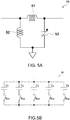
- the matching circuit 11 included in the RF tag 10 according to this embodiment, as illustrated in Fig. 5A is a circuit including two inductors 51 and 52 and a variable-capacitance capacitor 53 of which a capacitance can be changed in accordance with a control signal supplied from the outside.
- the matching circuit 11 uses a circuit combining capacitors C 1 to C 5 having mutually-different capacitance values and switches S C1 to S C5 as illustrated in Fig. 5B as the variable-capacitance capacitor 53.
- the matching circuit 11 may be a circuit that has a different circuit configuration (for example, a circuit configured such that the capacity of an inductor can be changed) as long as it is a circuit of which an impedance can be changed using a control signal supplied from the outside.
- the demodulation circuit 12 ( Fig. 4 ) is a circuit that extracts a command transmitted by a reader/writer (R/W) 85 (host device 90) from a radio wave received by the antenna 20 by demodulating an output of the antenna 20 that is input through the matching circuit 11.
- the modulation circuit 14 is a circuit that is used for transmitting information to the reader/writer 85 by performing modulation according to the information to be notified to the reader/writer 85 for a reflected wave of a carrier wave transmitted from an antenna 80 of the reader/writer 85.
- the rectification circuit 13 is a circuit that generates DC power used for operating each unit (the demodulation circuit 12, the modulation circuit 14, the load 25, and the like) disposed inside the RF tag 10 by rectifying AC power output by the antenna 20 that has received the radio wave.
- this rectification circuit 13 for example, a circuit having a configuration illustrated in Fig. 6 , in other words, a diode charge pump in which unit rectification circuits 55 1 to 55 N each configured by two diodes (D1 and D2 or the like) and a capacitor C (C1 and C2 or the like) are connected in N stages is used.
- the rectification circuit 13 may a circuit that can output a voltage for the load 25 and a voltage for circuits other than the load 25.
- the load 25 is an electronic circuit (a sensor, an LED, an IC, a microcomputer, or the like) used by the host device 90 through the reader/writer (R/W) 85.
- a power supply voltage VOUT is supplied to the load 25 through a first switch 22 of a normally-on type that can be controlled such that it is turned on/off by the control unit 18.
- the variable load 21 is a circuit of which the power consumption amount can be changed.
- the power supply voltage VOUT is supplied to the variable load 21 through a second switch 23 of a normally-off type that can be controlled such that it is turned on/off by the control unit 18.
- a variable resistance circuit of which the resistance value can be changed (designated) using a control signal is used.
- the limiter 16 ( Fig. 4 ) is a circuit that limits the output voltage of the rectification circuit 13 to a predetermined voltage (hereinafter, also represented as a limiter voltage VLIM or a saturation voltage) or less.
- the ADC 17 is an AD converter that digitalizes the output voltage of the rectification circuit 13.
- the impedance adjustment control circuit 15 is a circuit that outputs a control signal (in this embodiment, a control signal designating the capacitance of the variable-capacitance capacitor 53 ( Fig. 5B )) designating the impedance of the matching circuit 11.
- a control signal in this embodiment, a control signal designating the capacitance of the variable-capacitance capacitor 53 ( Fig. 5B ) designating the impedance of the matching circuit 11.
- the impedance adjustment control circuit 15 having the configuration illustrated in Fig. 6 is used.
- an up counter 61 is a counter that clears a count value to "0" when a Reset pulse is input and counts up when an up pulse is input.
- the counter value of the up counter 61 is used as a control signal designating the impedance (the capacitance of the variable-capacitance capacitor 53 ( Fig. 4B) ) of the matching circuit 11.
- a comparator 62 is a circuit that outputs a result of comparison between the power supply voltage (the output voltage of the rectification circuit 13) VOUT and the voltage of a capacitor 63.
- the output of the comparator 62 is input to the control unit 18 through a CMP_OUT signal line.
- the switch 64 is a switch that is controlled to be turned on/off by the control unit 18 through a Ctrl signal line.
- the control unit 18 is a unit, which is configured of a processor (a CPU or the like), responding to a command extracted by the demodulation circuit 12 by controlling the demodulation circuit 14 and the like.
- the control unit 18 is configured (programmed) such that it can execute an impedance optimization process of a flow illustrated in Fig. 8 .
- An execution timing of the impedance optimization process is not particularly limited. Accordingly, for example, the control unit 18 may be configured such that it executes the impedance optimization process when the power supply voltage becomes a threshold value or less, or the control unit 18 may be configured such that it executes the impedance optimization process when the execution of the impedance optimization process is directed from the reader/writer 85.
- the control unit 18 when the impedance optimization process is started, the control unit 18, first, performs a process of turning off the first switch 22 and turning on the second switch 23 (Step S101). In other words, the control unit 18 performs a process for stopping supply of power to the load 25 and starting supply of power to the variable load 21.
- the control unit 18 measures the power supply voltage VOUT by controlling the ADC 17 (Step S102). Thereafter, the control unit 18 determines whether or not the power supply voltage VOUT is equal to or less than a voltage VREF (Step S103).
- the voltage VREF is a voltage that is less than the limiter voltage VLIM set in advance.
- Step S107 the control unit 18 performs a process of changing the amount of power consumption of the variable load 21 in a direction in which the power supply voltage VOUT reduces (Step S107).
- the limiter 16 is disposed in a rear stage of the rectification circuit 13.
- the control unit 18 that has completed the process of Step S107 executes the process of Step S102 and subsequent steps again. Then, as a result of repeating the process of Steps S102, S103, and S107, the control unit 18 executes the impedance adjusting process (Step S104) in a case in which the power supply voltage VOUT becomes the voltage VREF or less (Step S103: Yes).
- the impedance adjusting process is a process of a flow illustrated in Fig. 9 .
- the control unit 18 that has started the impedance adjusting process, first, outputs a Reset pulse (Step S201). Accordingly, the count value of the up counter 61 disposed inside the impedance adjustment control circuit 15 (see Fig. 7 ) is Reset to "0", and the capacitance of the variable-capacitance capacitor 53 ( Fig. 5A ) disposed inside the matching circuit 11 is adjusted to the lowest capacitance C 0 .
- control unit 18 outputs a Ctrl pulse (Step S202).
- control unit 18 causes the voltage (an input voltage input to the "-" terminal of the comparator 62) of the capacitor 63 to coincide with the power supply voltage VOUT at that time point by turning on the switch 64 and then holds the voltage of the capacitor 63 by turning off the switch 64.
- control unit 18 outputs an up pulse (Step S203) and then determines whether or not the output CMP_OUT of the comparator 62 is low (Step S204).
- the up pulse When the up pulse is input, the count value of the up counter 61 is counted up, and accordingly, the capacitance of the variable-capacitance capacitor 53 disposed inside the matching circuit 11 increases.
- the capacitance of the variable-capacitance capacitor 53 increases, the power supply voltage increases in a case in which the impedance of the matching circuit 11 does not have an appropriate value and the power supply voltage is not limited by the limiter 16.
- the impedance of the matching circuit 11 has an appropriate value and the power supply voltage is limited by the limiter 16
- the power supply voltage hardly changes.
- Step S204: No the control unit 18 returns the process to Step S203 and outputs the up pulse again. Then, when the output CMP_OUT of the comparator 62 becomes low (Step S204: Yes), the control unit 18 ends the impedance adjusting process (the process illustrated in Fig. 9 ).
- the control unit 18 that has ended impedance adjusting process (Step S104) measures the power supply voltage VOUT (Step S105) and determines whether or not the power supply voltage VOUT is less than the limiter voltage VLIM (Step S106). In a case in which the power supply voltage VOUT is not less than the limiter voltage VLIM (Step S106: No), the control unit 18 re-executes the process of Step S102 and subsequent steps.
- Step S106 when the power supply voltage VOUT becomes less than the limiter voltage VLIM during the repetition of the process described above (Step S106: Yes), the control unit 18 performs a process of turning off the second switch 23 and turning on the first switch 22 (Step S108) and then ends this impedance optimization process (the process illustrated in Fig 8 ).
- the control unit 18 determines whether or not the amount of power consumption of the variable load 21 at that time point is an upper limit amount.
- the control unit 18 causes the process to proceed to Step S107 and increase the amount of power consumption of the variable load 21.
- the control unit 18 performs the process of Step S108 and then ends this impedance optimization process.
- the control unit 18 is configured such that it performs the impedance optimization process of the sequence described above.
- the impedance optimization process is started in a state in which the power supply voltage VOUT is less than the limiter voltage VLIM, as illustrated in Fig. 10 .
- the first switch 22 and the second switch 23 are controlled such that a state is formed in which power is not supplied to the load 25, and power is supplied to the variable load 21.
- the power supply voltage VOUT is reduced to the voltage VREF.
- the power supply voltage VOUT after the impedance adjusting process is not less than the limiter voltage VLIM, as illustrated in Fig. 10 , again, the power supply voltage VOUT is reduced to the voltage VREF in accordance with adjustment of the amount of power consumption of the variable load 21. Thereafter, the impedance adjusting process is performed. Then, it is determined whether or not the power supply voltage VOUT after the impedance adjusting process is less than the limiter voltage VLIM. In a case in which the power supply voltage VOUT is less than the limiter voltage VLIM, the first switch 22 and the second switch 23 are controlled such that the state is returned to the original state in which power is not supplied to the variable load 21, and power is supplied to the load 25, and the impedance optimization process ends.
- the power supply voltage after the impedance adjusting process being less than the limiter voltage VLIM represents that the impedance of the matching circuit 11 has an optimal value. More specifically, as illustrated in Fig. 11 , a power supply voltage - capacitance curve (broken line) of a case in which the limiter 16 is not disposed represents that a peak voltage changes to a lower side in accordance with an increase in the amount of power consumption of the variable load 21.
- the impedance adjusting process ( Fig. 8 ) is a process of adjusting the capacitance of the variable-capacitance capacitor 53 to a capacitance for which the power supply voltage is a maximum. Accordingly, in a case in which the power supply voltage after the impedance adjusting process is less than the limiter voltage VLIM, the impedance of the matching circuit 11 has an optimal value.
- the RF tag 10 has a function of adjusting the impedance of the matching circuit 11 to an optimal value. Accordingly, by using the RF tag 10, a radio communication system that is robust with respect to environmental changes, in other words, a radio communication system in which it is difficult for an obstacle to occur in communication with the reader/writer 85 even when power input to the RF tag 10 is reduced in accordance with environmental changes can be built.
- the RF tag 10 may be modified into a device in which the variable load 21 is not included, and the unit described above is used as the variable load 21.
- the RF tag 10 may be modified into a device not including the first switch 22 and/or the second switch 23.
- a process of adjusting the power consumption of the variable load 21 to "0" (or minimum power consumption) may be performed in Step S108.
- the RF tag 10 may be modified to a multi-level comparator comparing the power supply voltage VOUT with the voltage VREF and comparing the power supply voltage VOUT with the limiter voltage VLIM instead of the ADC 17.
- the RF tag 10 may be modified into a device that includes a comparator comparing the power supply voltage VOUT with the voltage VREF and a comparator comparing the power supply voltage VOUT with the limiter voltage VLIM instead of the ADC 17.
- a function for executing a second impedance adjusting process (an impedance adjusting process in which the process of Step S101 is not performed) starting adjustment of the impedance of the matching circuit 11 from the impedance at that time point may be included in the RF tag 10, and the impedance optimization process may be changed to the process in which the second impedance adjusting process is performed in the second and subsequent Step S105.
- the impedance optimization process ( Fig. 8 ) may be modified to a process in which the process of Step S106 is not performed, that is, a process in which, after the power supply voltage VOUT is reduced to a voltage less than the limiter voltage VLIM (a voltage that is VREF or less), the impedance adjusting process is performed only once.
- the condition for ending the impedance optimization process may be changed to a condition other than "VOUT ⁇ VLIM", for example, "the number of times of execution of the impedance adjusting process ⁇ a predetermined number of times" or "an execution time of the impedance optimization process (an elapsed time after the start of the impedance optimization process) ⁇ a predetermined number of times".
- a comparator comparing the power supply voltage VOUT with the voltage VREF may be used instead of the ADC 17.
- the impedance of the matching circuit 11 may not be adjusted to the optimal value in some cases. Even in a case in which the condition for ending the impedance optimization process is changed to the condition described above, the impedance of the matching circuit 11 can be adjusted more satisfactorily than in a conventional case (a form in which a result of the adjustment of the impedance is closer to the optimal value than that of the conventional case).
- the impedance adjusting process described above is a process in which the capacitance of the variable-capacitance capacitor 53 for which the impedance of the matching circuit 11 has an optimal value (hereinafter, referred to as optimal capacitance) is retrieved through a linear search of monotonously increasing the capacitance of the variable-capacitance capacitor 53 ( Fig. 5A )
- the impedance adjusting process may be a process in which an optimal capacitance of the variable-capacitance capacitor 53 is retrieved through a linear search monotonously reducing the capacitance of the variable-capacitance capacitor 53.
- the impedance adjusting process may be a process of retrieving the optimal capacitance of the variable-capacitance capacitor 53 using another search algorithm such as a binary search or a tree search.
- a process using various search algorithms may be employed.
- a function of monitoring the power supply voltage VOUT being a predetermined voltage, which is less than the voltage VLIM, or less and performing an impedance adjusting process when the power supply voltage VOUT becomes the predetermined voltage or less may be given to the RF tag 10.
- the RF tag 10 may be modified into a device, which has the function described above, not performing the impedance optimization process.
Landscapes
- Engineering & Computer Science (AREA)
- Computer Hardware Design (AREA)
- Microelectronics & Electronic Packaging (AREA)
- Physics & Mathematics (AREA)
- Theoretical Computer Science (AREA)
- General Physics & Mathematics (AREA)
- Electromagnetism (AREA)
- Computer Networks & Wireless Communication (AREA)
- Computer Security & Cryptography (AREA)
- General Engineering & Computer Science (AREA)
- Power Engineering (AREA)
- Near-Field Transmission Systems (AREA)
- Details Of Aerials (AREA)
Abstract
Description
- The present invention relates to an RF tag.
- In recent years, the development of RF tags has been remarkable, and RF tags are used for mounting wireless electronic components by applying a wireless power transmission function in addition to their original use of object identification. In such applications, electrical loads such as a CPU and a sensor are included as wireless electronic components, and it is preferable to further increase the electric power received by the RF tags such that electric power is stably supplied for operations of such loads. As an RF tag that realizes the effect described above, an RF tag in which a matching circuit having variable impedance (variable impedance circuit) is disposed in a front stage of a rectification circuit is known.
- In such an RF tag, in a case in which a deviation of the impedance of the matching circuit from an optimal value is large, an output voltage of the rectification circuit (hereinafter, also expressed as a power supply voltage) may be easily caused to be equal to or less than an operation lower limit voltage of each circuit included in the RF tag in accordance with environmental changes. More specifically, since the impedance of the matching circuit is adjusted to an optimal value, an RF tag having a power supply margin of 7 dB will be considered. Here, a power supply margin is the reduced amount of input power that causes a power supply voltage (the output voltage of the rectification circuit) to be reduced to the operation lower limit voltage in units of dB.
- In a case in which input power to the RF tag drops by 6 dB due to an environmental change (appearance of an obstacle inhibiting the propagation of radio waves toward the antenna, water adhesion to the antenna, or the like), as illustrated in
Fig. 1A , the power supply voltage is lowered but not to the operation lower limit voltage. Accordingly, the RF tag continues to operate. - On the other hand, in a case in which the impedance of the matching circuit is not adjusted to an optimal value, and thus, the power supply margin of the RF tag is only 4 dB, as illustrated in
Fig. 1B , when the input power drops by 6 dB, the power supply voltage becomes equal to or lower than the operation lower limit voltage. As a result, the RF tag does not operate. - In this way, in a case in which a deviation of the impedance of the matching circuit from the optimal value is large, the power supply voltage may be easily caused to be equal to or lower than the operation lower limit voltage of each circuit included in the RF tag due to environmental change. For this reason, it is preferable to satisfactorily adjust the impedance of the matching circuit included in the RF tag.
- Meanwhile, the impedance of the matching circuit included in the RF tag is, generally, adjusted such that the output voltage of the rectification circuit is maximal (for example, see Japanese Patent Application Laid-open No.
H7-111470 Fig. 2 , in an RF tag including a limiter that is used for preventing application of an excessive voltage to each circuit or the like, the power supply voltage is limited by the limiter. For this reason, in the adjustment process described above, the impedance of the matching circuit of the RF tag cannot be adjusted to the optimal value. - More specifically, as the matching circuit, generally, a circuit (see
Fig. 5A ) combining two inductors and a variable-capacitance capacitor is employed. In addition, as the adjustment process, generally, a process in which the capacitance C of the variable-capacitance capacitor included in the matching circuit is reduced to a certain value C0, and the capacitance C is increased until the power supply voltage does not change is performed. Accordingly, in a case in which the impedance of the matching circuit of the RF tag including a limiter is adjusted in the adjustment process, as schematically illustrated inFig. 3 , the adjustment of the impedance (the capacitance C of the variable-capacitance capacitor) of the matching circuit ends in a stage in which the power supply voltage rises up to a saturation voltage (limiter voltage), and thus, the impedance of the matching circuit cannot be adjusted to the optimal value. - The invention is in view of the current situation described above, and an object thereof is to provide an RF tag that is an RF tag including a limiter and is capable of satisfactorily adjusting the impedance of a matching circuit.
- In order to achieve the objective described above, according to the invention, there is provided an RF tag to which power is wirelessly fed from a reader/writer including: a rectification circuit that rectifies an AC signal supplied from an antenna and outputs a DC voltage supplied to each unit inside the RF tag as a power supply voltage; a limiter that limits the output voltage of the rectification circuit to a predetermined voltage or less; a matching circuit, of which an impedance is changeable, disposed between the antenna and the rectification circuit; a variable load unit, of which an amount of power consumption is changeable, consuming power output from the rectification circuit; and a control unit that is capable of executing an impedance adjusting process of adjusting the impedance of the matching circuit such that the output voltage of the rectification circuit increases and executes the impedance adjusting process after reducing the output voltage of the rectification circuit to a voltage less than the predetermined voltage by adjusting the amount of power consumption of the variable load unit when a predetermined condition is satisfied.
- In other words, "an impedance adjusting process of adjusting the impedance of the matching circuit such that the output voltage of the rectification circuit increases" is a process in which more satisfactory adjustment of the impedance can be achieved when the process is performed after the output voltage of the rectification circuit is decreased to a voltage that is not limited by the limiter. The RF tag according to the invention has a function of "executing the impedance adjusting process after reducing the output voltage of the rectification circuit to a voltage less than the predetermined voltage by adjusting the amount of power consumption of the variable load unit". Therefore, according to the invention, an RF tag including a limiter and is capable of satisfactorily adjusting the impedance of the matching circuit can be realized.
- In addition, the variable load unit of the RF tag according to the invention may include a variable load for impedance adjustment (for adjustment of the amount of power consumption) and a load (an IC, a sensor, or the like) for the original use of the RF tag or may include only a variable load for impedance adjustment (for adjustment of the amount of power consumption). Furthermore, the "predetermined condition" according to the invention may be any condition. More specifically, the "predetermined condition", for example, may be a condition that "a predetermined time has elapsed after previous adjustment of impedance was performed", a condition that "a predetermined direction is input from another device (a reader/writer or the like), or a condition that "the power supply voltage becomes less than the limiter voltage".
- The RF tag according to the invention may employ a configuration in which "the control unit repeats the process of executing the impedance adjusting process after reducing the output voltage of the rectification circuit to the voltage less than the predetermined voltage by adjusting the amount of power consumption of the variable load unit when the predetermined condition is satisfied until the output voltage of the rectification circuit after the process becomes a voltage less than the predetermined voltage". In addition, the RF tag according to the invention may employ a configuration in which "the variable load unit is a unit of which a resistance value is changeable, and the control unit repeats the process of executing the impedance adjusting process after reducing the output voltage of the rectification circuit to the voltage less than the predetermined voltage by adjusting the amount of power consumption of the variable load unit when the predetermined condition is satisfied until the resistance value of the variable load unit after the process becomes a predetermined value or less" or a configuration in which "the control unit repeats the process of executing the impedance adjusting process after reducing the output voltage of the rectification circuit to the voltage less than the predetermined voltage by adjusting the amount of power consumption of the variable load unit when the predetermined condition is satisfied a predetermined number of times or until a predetermined time elapses. By employing such a configuration, an RF tag capable of adjusting the impedance of the matching circuit more satisfactorily is acquired.
- According to the invention, an RF tag including a limiter and is capable of satisfactorily adjusting the impedance of a matching circuit can be provided.
-
-
Fig. 1A is an explanatory diagram illustrating change in a pattern of a power supply voltage over time when an environment change occurs in an RF tag in which an impedance of a matching circuit is adjusted to an optimal value; -
Fig. 1B is an explanatory diagram illustrating a change in a pattern of a power supply voltage over time when an environment change occurs in an RF tag in which an impedance of a matching circuit is not adjusted to an optimal value; -
Fig. 2 is a configuration diagram of an RF tag that includes a limiter; -
Fig. 3 is a diagram illustrating problems in a conventional adjustment process; -
Fig. 4 is an explanatory diagram illustrating the configuration and the use form of an RF tag according to one embodiment of the invention; -
Fig. 5A is an explanatory diagram illustrating the configuration of a matching circuit included in an RF tag; -
Fig. 5B is an explanatory diagram illustrating the configuration of a variable-capacitance capacitor disposed inside a matching circuit; -
Fig. 6 is a block diagram of a rectification circuit included in an RF tag; -
Fig. 7 is an explanatory diagram illustrating the configuration of an impedance adjustment control circuit included in an RF tag; -
Fig. 8 is a flowchart illustrating an impedance optimization process executed by a control unit disposed in an RF tag; -
Fig. 9 is a flowchart illustrating an impedance adjusting process executed during the impedance optimization process; -
Fig. 10 is an explanatory diagram illustrating an impedance optimization process; and -
Fig. 11 is a diagram illustrating a reason why the impedance of a matching circuit can be adjusted to an optimal value using an impedance optimization process. - Hereinafter, an embodiment of the invention will be described with reference to the drawings.
-
Fig. 4 illustrates the configuration and the use form of anRF tag 10 according to one embodiment of the invention. As illustrated in the drawing, theRF tag 10 includes amatching circuit 11, ademodulation circuit 12, arectification circuit 13, amodulation circuit 14, an impedanceadjustment control circuit 15, alimiter 16, anADC 17, acontrol unit 18, avariable load 21, and aload 25. - The matching
circuit 11 is a variable impedance circuit used for impedance matching between anantenna 20 and a circuit disposed inside theRF tag 10. Thematching circuit 11 included in theRF tag 10 according to this embodiment, as illustrated inFig. 5A , is a circuit including twoinductors capacitance capacitor 53 of which a capacitance can be changed in accordance with a control signal supplied from the outside. Thematching circuit 11 uses a circuit combining capacitors C1 to C5 having mutually-different capacitance values and switches SC1 to SC5 as illustrated inFig. 5B as the variable-capacitance capacitor 53. Here, the matchingcircuit 11 may be a circuit that has a different circuit configuration (for example, a circuit configured such that the capacity of an inductor can be changed) as long as it is a circuit of which an impedance can be changed using a control signal supplied from the outside. - The demodulation circuit 12 (
Fig. 4 ) is a circuit that extracts a command transmitted by a reader/writer (R/W) 85 (host device 90) from a radio wave received by theantenna 20 by demodulating an output of theantenna 20 that is input through the matchingcircuit 11. Themodulation circuit 14 is a circuit that is used for transmitting information to the reader/writer 85 by performing modulation according to the information to be notified to the reader/writer 85 for a reflected wave of a carrier wave transmitted from anantenna 80 of the reader/writer 85. - The
rectification circuit 13 is a circuit that generates DC power used for operating each unit (thedemodulation circuit 12, themodulation circuit 14, theload 25, and the like) disposed inside theRF tag 10 by rectifying AC power output by theantenna 20 that has received the radio wave. As thisrectification circuit 13, for example, a circuit having a configuration illustrated inFig. 6 , in other words, a diode charge pump in which unit rectification circuits 551 to 55N each configured by two diodes (D1 and D2 or the like) and a capacitor C (C1 and C2 or the like) are connected in N stages is used. In addition, therectification circuit 13 may a circuit that can output a voltage for theload 25 and a voltage for circuits other than theload 25. - The
load 25 is an electronic circuit (a sensor, an LED, an IC, a microcomputer, or the like) used by thehost device 90 through the reader/writer (R/W) 85. A power supply voltage VOUT is supplied to theload 25 through afirst switch 22 of a normally-on type that can be controlled such that it is turned on/off by thecontrol unit 18. - The
variable load 21 is a circuit of which the power consumption amount can be changed. The power supply voltage VOUT is supplied to thevariable load 21 through asecond switch 23 of a normally-off type that can be controlled such that it is turned on/off by thecontrol unit 18. As thevariable load 21, for example, a variable resistance circuit of which the resistance value can be changed (designated) using a control signal is used. - The limiter 16 (
Fig. 4 ) is a circuit that limits the output voltage of therectification circuit 13 to a predetermined voltage (hereinafter, also represented as a limiter voltage VLIM or a saturation voltage) or less. TheADC 17 is an AD converter that digitalizes the output voltage of therectification circuit 13. - The impedance
adjustment control circuit 15 is a circuit that outputs a control signal (in this embodiment, a control signal designating the capacitance of the variable-capacitance capacitor 53 (Fig. 5B )) designating the impedance of the matchingcircuit 11. In theRF tag 10 according to this embodiment, the impedanceadjustment control circuit 15 having the configuration illustrated inFig. 6 is used. - Although the overall operation of the impedance
adjustment control circuit 15 will be described later, an upcounter 61 is a counter that clears a count value to "0" when a Reset pulse is input and counts up when an up pulse is input. The counter value of theup counter 61 is used as a control signal designating the impedance (the capacitance of the variable-capacitance capacitor 53 (Fig. 4B) ) of the matchingcircuit 11. - A comparator 62 is a circuit that outputs a result of comparison between the power supply voltage (the output voltage of the rectification circuit 13) VOUT and the voltage of a
capacitor 63. The output of the comparator 62 is input to thecontrol unit 18 through a CMP_OUT signal line. Theswitch 64 is a switch that is controlled to be turned on/off by thecontrol unit 18 through a Ctrl signal line. - The
control unit 18 is a unit, which is configured of a processor (a CPU or the like), responding to a command extracted by thedemodulation circuit 12 by controlling thedemodulation circuit 14 and the like. - The
control unit 18 is configured (programmed) such that it can execute an impedance optimization process of a flow illustrated inFig. 8 . An execution timing of the impedance optimization process is not particularly limited. Accordingly, for example, thecontrol unit 18 may be configured such that it executes the impedance optimization process when the power supply voltage becomes a threshold value or less, or thecontrol unit 18 may be configured such that it executes the impedance optimization process when the execution of the impedance optimization process is directed from the reader/writer 85. - As illustrated in
Fig. 8 , when the impedance optimization process is started, thecontrol unit 18, first, performs a process of turning off thefirst switch 22 and turning on the second switch 23 (Step S101). In other words, thecontrol unit 18 performs a process for stopping supply of power to theload 25 and starting supply of power to thevariable load 21. - Next, the
control unit 18 measures the power supply voltage VOUT by controlling the ADC 17 (Step S102). Thereafter, thecontrol unit 18 determines whether or not the power supply voltage VOUT is equal to or less than a voltage VREF (Step S103). Here, the voltage VREF is a voltage that is less than the limiter voltage VLIM set in advance. - In a case in which the power supply voltage VOUT is not the voltage VREF or less (Step S103: No), the
control unit 18 performs a process of changing the amount of power consumption of thevariable load 21 in a direction in which the power supply voltage VOUT reduces (Step S107). In addition, thelimiter 16 is disposed in a rear stage of therectification circuit 13. Thus, there are also cases in which the power supply voltage VOUT does not decrease even when the process of Step S107 is performed. - The
control unit 18 that has completed the process of Step S107 executes the process of Step S102 and subsequent steps again. Then, as a result of repeating the process of Steps S102, S103, and S107, thecontrol unit 18 executes the impedance adjusting process (Step S104) in a case in which the power supply voltage VOUT becomes the voltage VREF or less (Step S103: Yes). - The impedance adjusting process is a process of a flow illustrated in
Fig. 9 . - In other words, the
control unit 18 that has started the impedance adjusting process, first, outputs a Reset pulse (Step S201). Accordingly, the count value of the up counter 61 disposed inside the impedance adjustment control circuit 15 (seeFig. 7 ) is Reset to "0", and the capacitance of the variable-capacitance capacitor 53 (Fig. 5A ) disposed inside the matchingcircuit 11 is adjusted to the lowest capacitance C0. - Next, the
control unit 18 outputs a Ctrl pulse (Step S202). In other words, thecontrol unit 18 causes the voltage (an input voltage input to the "-" terminal of the comparator 62) of thecapacitor 63 to coincide with the power supply voltage VOUT at that time point by turning on theswitch 64 and then holds the voltage of thecapacitor 63 by turning off theswitch 64. - Thereafter, the
control unit 18 outputs an up pulse (Step S203) and then determines whether or not the output CMP_OUT of the comparator 62 is low (Step S204). - When the up pulse is input, the count value of the
up counter 61 is counted up, and accordingly, the capacitance of the variable-capacitance capacitor 53 disposed inside the matchingcircuit 11 increases. When the capacitance of the variable-capacitance capacitor 53 increases, the power supply voltage increases in a case in which the impedance of the matchingcircuit 11 does not have an appropriate value and the power supply voltage is not limited by thelimiter 16. On the other hand, in a case in which the impedance of the matchingcircuit 11 has an appropriate value and the power supply voltage is limited by thelimiter 16, even when the capacitance of the variable-capacitance capacitor 53 increases, the power supply voltage hardly changes. Thus, in a case in which the output CMP_OUT is low, the adjustment of the impedance of the matchingcircuit 11 is completed. However, in a case in which the output CMP_OUT is high, the adjustment of the impedance of the matchingcircuit 11 is not completed. - For this reason, in a case in which the output CMP_OUT of the comparator 62 is high (Step S204: No), the
control unit 18 returns the process to Step S203 and outputs the up pulse again. Then, when the output CMP_OUT of the comparator 62 becomes low (Step S204: Yes), thecontrol unit 18 ends the impedance adjusting process (the process illustrated inFig. 9 ). - The description of the impedance optimization process will be continued with reference back to
Fig. 8 . - The
control unit 18 that has ended impedance adjusting process (Step S104) measures the power supply voltage VOUT (Step S105) and determines whether or not the power supply voltage VOUT is less than the limiter voltage VLIM (Step S106). In a case in which the power supply voltage VOUT is not less than the limiter voltage VLIM (Step S106: No), thecontrol unit 18 re-executes the process of Step S102 and subsequent steps. - Then, when the power supply voltage VOUT becomes less than the limiter voltage VLIM during the repetition of the process described above (Step S106: Yes), the
control unit 18 performs a process of turning off thesecond switch 23 and turning on the first switch 22 (Step S108) and then ends this impedance optimization process (the process illustrated inFig 8 ). Although not illustrated in the flowchart (Fig. 8 ), in a case in which the power supply voltage VOUT is not less than the limiter voltage VLIM, thecontrol unit 18 determines whether or not the amount of power consumption of thevariable load 21 at that time point is an upper limit amount. Then, in a case in which the amount of power consumption of thevariable load 21 is not the upper limit amount (in other words, in a case in which the amount of power consumption of thevariable load 21 can be increased), thecontrol unit 18 causes the process to proceed to Step S107 and increase the amount of power consumption of thevariable load 21. On the other hand, in a case in which the amount of power consumption of thevariable load 21 is the upper limit amount, thecontrol unit 18 performs the process of Step S108 and then ends this impedance optimization process. - The
control unit 18 is configured such that it performs the impedance optimization process of the sequence described above. Thus, in a case in which the impedance optimization process is started in a state in which the power supply voltage VOUT is less than the limiter voltage VLIM, as illustrated inFig. 10 , first, thefirst switch 22 and thesecond switch 23 are controlled such that a state is formed in which power is not supplied to theload 25, and power is supplied to thevariable load 21. Next, in accordance with adjustment of the amount of power consumption of thevariable load 21, the power supply voltage VOUT is reduced to the voltage VREF. Then, after the impedance adjusting process is performed, it is determined whether or not the power supply voltage VOUT after the impedance adjusting process is less than the limiter voltage VLIM. - In a case in which the power supply voltage VOUT after the impedance adjusting process is not less than the limiter voltage VLIM, as illustrated in
Fig. 10 , again, the power supply voltage VOUT is reduced to the voltage VREF in accordance with adjustment of the amount of power consumption of thevariable load 21. Thereafter, the impedance adjusting process is performed. Then, it is determined whether or not the power supply voltage VOUT after the impedance adjusting process is less than the limiter voltage VLIM. In a case in which the power supply voltage VOUT is less than the limiter voltage VLIM, thefirst switch 22 and thesecond switch 23 are controlled such that the state is returned to the original state in which power is not supplied to thevariable load 21, and power is supplied to theload 25, and the impedance optimization process ends. - The power supply voltage after the impedance adjusting process being less than the limiter voltage VLIM represents that the impedance of the matching
circuit 11 has an optimal value. More specifically, as illustrated inFig. 11 , a power supply voltage - capacitance curve (broken line) of a case in which thelimiter 16 is not disposed represents that a peak voltage changes to a lower side in accordance with an increase in the amount of power consumption of thevariable load 21. The impedance adjusting process (Fig. 8 ) is a process of adjusting the capacitance of the variable-capacitance capacitor 53 to a capacitance for which the power supply voltage is a maximum. Accordingly, in a case in which the power supply voltage after the impedance adjusting process is less than the limiter voltage VLIM, the impedance of the matchingcircuit 11 has an optimal value. - As described above, the
RF tag 10 according to this embodiment has a function of adjusting the impedance of the matchingcircuit 11 to an optimal value. Accordingly, by using theRF tag 10, a radio communication system that is robust with respect to environmental changes, in other words, a radio communication system in which it is difficult for an obstacle to occur in communication with the reader/writer 85 even when power input to theRF tag 10 is reduced in accordance with environmental changes can be built. - Various modifications can be made in the
RF tag 10 according to the embodiment described above. For example, in a case in which there is a unit of which the amount of power consumption can be adjusted relatively finely among power supply targets in the RF tag 10 (theload 25, thecontrol unit 18, thedemodulation circuit 12, themodulation circuit 14, the impedanceadjustment control circuit 15, and the like), theRF tag 10 may be modified into a device in which thevariable load 21 is not included, and the unit described above is used as thevariable load 21. In addition, theRF tag 10 may be modified into a device not including thefirst switch 22 and/or thesecond switch 23. Furthermore, in a case in which theRF tag 10 is modified into a device not including thesecond switch 23, a process of adjusting the power consumption of thevariable load 21 to "0" (or minimum power consumption) may be performed in Step S108. - The
RF tag 10 may be modified to a multi-level comparator comparing the power supply voltage VOUT with the voltage VREF and comparing the power supply voltage VOUT with the limiter voltage VLIM instead of theADC 17. In addition, theRF tag 10 may be modified into a device that includes a comparator comparing the power supply voltage VOUT with the voltage VREF and a comparator comparing the power supply voltage VOUT with the limiter voltage VLIM instead of theADC 17. - Furthermore, a function for executing a second impedance adjusting process (an impedance adjusting process in which the process of Step S101 is not performed) starting adjustment of the impedance of the matching
circuit 11 from the impedance at that time point may be included in theRF tag 10, and the impedance optimization process may be changed to the process in which the second impedance adjusting process is performed in the second and subsequent Step S105. - The impedance optimization process (
Fig. 8 ) may be modified to a process in which the process of Step S106 is not performed, that is, a process in which, after the power supply voltage VOUT is reduced to a voltage less than the limiter voltage VLIM (a voltage that is VREF or less), the impedance adjusting process is performed only once. The condition for ending the impedance optimization process may be changed to a condition other than "VOUT < VLIM", for example, "the number of times of execution of the impedance adjusting process < a predetermined number of times" or "an execution time of the impedance optimization process (an elapsed time after the start of the impedance optimization process) < a predetermined number of times". In addition, in a case in which a condition of not using the power supply voltage VOUT is used as the condition for ending the impedance optimization process, a comparator comparing the power supply voltage VOUT with the voltage VREF may be used instead of theADC 17. - When the condition for ending the impedance optimization process is changed to the condition described above, the impedance of the matching
circuit 11 may not be adjusted to the optimal value in some cases. Even in a case in which the condition for ending the impedance optimization process is changed to the condition described above, the impedance of the matchingcircuit 11 can be adjusted more satisfactorily than in a conventional case (a form in which a result of the adjustment of the impedance is closer to the optimal value than that of the conventional case). - While the impedance adjusting process described above is a process in which the capacitance of the variable-
capacitance capacitor 53 for which the impedance of the matchingcircuit 11 has an optimal value (hereinafter, referred to as optimal capacitance) is retrieved through a linear search of monotonously increasing the capacitance of the variable-capacitance capacitor 53 (Fig. 5A ), the impedance adjusting process may be a process in which an optimal capacitance of the variable-capacitance capacitor 53 is retrieved through a linear search monotonously reducing the capacitance of the variable-capacitance capacitor 53. In addition, the impedance adjusting process may be a process of retrieving the optimal capacitance of the variable-capacitance capacitor 53 using another search algorithm such as a binary search or a tree search. Also in an impedance adjusting process of anRF tag 10 in which thematching circuit 11 is a circuit of which the impedance can be adjusted by changing the capacity of an inductor, similarly, a process using various search algorithms may be employed. - A function of monitoring the power supply voltage VOUT being a predetermined voltage, which is less than the voltage VLIM, or less and performing an impedance adjusting process when the power supply voltage VOUT becomes the predetermined voltage or less may be given to the
RF tag 10. In addition, theRF tag 10 may be modified into a device, which has the function described above, not performing the impedance optimization process. -
- 10 RF tag
- 11 Matching circuit
- 12 Demodulation circuit
- 13 Rectification circuit
- 14 Modulation circuit
- 15 Impedance adjustment control circuit
- 16 Limiter
- 17 ADC
- 18 Control unit
- 20, 80 Antenna
- 21 Variable load
- 22 First switch
- 23 Second switch
- 25 Load
- 51, 52 Inductor
- 53 Variable-capacitance capacitor
- 551 to 55N Unit rectification circuit
- 61 Up counter
- 62 Comparator
- 63, C1 to C5, C2n-1, C2n Capacitor
- 64, SC1 to SC5 Switch
- 85 Reader/writer
- 90 Host device
- C Capacitance
- C0 Lowest capacitance
- CMP_OUT Output
- Ctrl Singal
- D1, D2, D3, D4, D2n Diode
- S101 ∼ S108, S201 ∼ S204 Steps
- VLIM Limiter voltage
- VOUT Power supply voltage
- VREF Voltage
Claims (4)
- An RF tag (10) to which power is wirelessly fed from a reader/writer (85), characterized in that, the RF tag (10) comprises:a rectification circuit (13) that rectifies an AC signal supplied from an antenna (20) and outputs a DC voltage (VOUT) supplied to each unit inside the RF tag (10) as a power supply voltage;a limiter (16) that limits the output voltage of the rectification circuit (13) to a predetermined voltage or less;a matching circuit (11), of which an impedance is changeable, disposed between the antenna (20) and the rectification circuit (13);a variable load unit (21), of which an amount of power consumption is changeable, consuming power output from the rectification circuit (13); anda control unit (18) that is capable of executing an impedance adjusting process of adjusting the impedance of the matching circuit (11) such that the output voltage of the rectification circuit (13) increases and executes the impedance adjusting process after reducing the output voltage of the rectification circuit (13) to a voltage less than the predetermined voltage by adjusting the amount of power consumption of the variable load unit (21) when a predetermined condition is satisfied.
- The RF tag (10) according to claim 1, characterized in that the control unit (18) repeats the process of executing the impedance adjusting process after reducing the output voltage of the rectification circuit (13) to the voltage less than the predetermined voltage by adjusting the amount of power consumption of the variable load unit (21) when the predetermined condition is satisfied until the output voltage of the rectification circuit (13) after the process becomes a voltage less than the predetermined voltage.
- The RF tag (10) according to claim 1, characterized in that the variable load unit (21) is a unit of which a resistance value is changeable, and the control unit (18) repeats the process of executing the impedance adjusting process after reducing the output voltage of the rectification circuit (13) to the voltage less than the predetermined voltage by adjusting the amount of power consumption of the variable load unit (21) when the predetermined condition is satisfied until the resistance value of the variable load unit (21) after the process becomes a predetermined value or less.
- The RF tag (10) according to claim 1, characterized in that the control unit (18) repeats the process of executing the impedance adjusting process after reducing the output voltage of the rectification circuit (13) to the voltage less than the predetermined voltage by adjusting the amount of power consumption of the variable load unit (21) when the predetermined condition is satisfied for a predetermined number of times or until a predetermined time elapses.
Applications Claiming Priority (1)
| Application Number | Priority Date | Filing Date | Title |
|---|---|---|---|
| JP2017177013A JP6844478B2 (en) | 2017-09-14 | 2017-09-14 | RF tag |
Publications (2)
| Publication Number | Publication Date |
|---|---|
| EP3457328A1 true EP3457328A1 (en) | 2019-03-20 |
| EP3457328B1 EP3457328B1 (en) | 2021-01-13 |
Family
ID=63311786
Family Applications (1)
| Application Number | Title | Priority Date | Filing Date |
|---|---|---|---|
| EP18188555.9A Active EP3457328B1 (en) | 2017-09-14 | 2018-08-10 | Rf tag |
Country Status (6)
| Country | Link |
|---|---|
| US (1) | US10572788B2 (en) |
| EP (1) | EP3457328B1 (en) |
| JP (1) | JP6844478B2 (en) |
| KR (1) | KR101999822B1 (en) |
| CN (1) | CN109508773B (en) |
| TW (1) | TWI668911B (en) |
Families Citing this family (5)
| Publication number | Priority date | Publication date | Assignee | Title |
|---|---|---|---|---|
| CN115001539A (en) * | 2019-04-11 | 2022-09-02 | 奈克赛特公司 | Wireless device configured to transmit power using harvested energy |
| US11748590B2 (en) * | 2020-12-18 | 2023-09-05 | Nxp B.V. | RFID tag with impedance tuning,and method of impedance tuning of an RRID tag |
| EP4275160B1 (en) | 2021-01-11 | 2025-05-07 | Nexite Ltd. | Contactless and automatic operations of a retail store |
| EP4449301A1 (en) | 2021-12-13 | 2024-10-23 | Nexite Ltd. | Systems, methods, and devices for contactless and automatic operation of retail stores |
| US20260101725A1 (en) * | 2024-10-09 | 2026-04-09 | Ap Memory Technology Corporation | Semiconductor device, testing system, and method for testing device under test on semiconductor wafer |
Citations (4)
| Publication number | Priority date | Publication date | Assignee | Title |
|---|---|---|---|---|
| JPH07111470A (en) | 1993-10-13 | 1995-04-25 | Tokai Rika Co Ltd | Receiver |
| US20080266729A1 (en) * | 2005-12-15 | 2008-10-30 | Nxp B.V. | Radio Frequency Interface Circuit for a Radio Frequency Identification Tag |
| US20140093016A1 (en) * | 2012-09-28 | 2014-04-03 | Kabushiki Kaisha Toshiba | Rectification circuit and wireless communication apparatus using the same |
| US20160004890A1 (en) * | 2014-07-02 | 2016-01-07 | Stmicroelectronics (Rousset) Sas | Voltage and power limiter for an electromagnetic transponder |
Family Cites Families (20)
| Publication number | Priority date | Publication date | Assignee | Title |
|---|---|---|---|---|
| JP3715518B2 (en) * | 2000-08-23 | 2005-11-09 | 日本電信電話株式会社 | Non-contact response device |
| US7538673B2 (en) * | 2005-08-26 | 2009-05-26 | Texas Instruments Incorporated | Voltage regulation circuit for RFID systems |
| KR100659272B1 (en) | 2005-12-15 | 2006-12-20 | 삼성전자주식회사 | Tag for wireless authentication capable of overvoltage control and its overvoltage control method |
| JP5236243B2 (en) * | 2006-10-18 | 2013-07-17 | 株式会社半導体エネルギー研究所 | RF tag |
| EP1914669B1 (en) * | 2006-10-18 | 2011-04-20 | Semiconductor Energy Laboratory Co., Ltd. | RFID tag |
| KR101210042B1 (en) * | 2006-12-11 | 2012-12-07 | 엘지이노텍 주식회사 | Radio Frequency IDentification tramceiver system |
| KR101044480B1 (en) * | 2009-08-17 | 2011-06-27 | 엘에스산전 주식회사 | RFID Tag |
| CN102244502A (en) * | 2011-04-25 | 2011-11-16 | 胡建国 | Automatic Q value adjustment amplitude limiting circuit |
| US9130369B2 (en) * | 2012-08-29 | 2015-09-08 | Qualcomm Incorporated | Wireless power overvoltage protection circuit with reduced power dissipation |
| CN102840925B (en) * | 2012-09-20 | 2014-03-19 | 卓捷创芯科技(深圳)有限公司 | Temperature measurement and correction circuit, passive radio frequency identification label and temperature measurement method |
| US8622313B1 (en) * | 2012-09-25 | 2014-01-07 | Cambridge Silicon Radio Limited | Near field communications device |
| KR20140112319A (en) * | 2013-03-13 | 2014-09-23 | 엘에스산전 주식회사 | Rfid reader based on automatic matching network and controlling method thereof |
| EP2963587B1 (en) * | 2014-07-04 | 2017-03-15 | Nxp B.V. | Voltage converter |
| JP2016100922A (en) * | 2014-11-18 | 2016-05-30 | キヤノン株式会社 | Power transmission device, power transmission device control method, and program |
| US9525412B2 (en) | 2015-02-18 | 2016-12-20 | Reno Technologies, Inc. | Switching circuit |
| EP3082072B1 (en) * | 2015-04-13 | 2017-12-27 | EM Microelectronic-Marin SA | Receiving unit of an rfid tag |
| CN106485290B (en) * | 2015-08-24 | 2019-08-13 | 瑞章科技有限公司 | Enhance the device and method of tag backscatter energy |
| CN106599972B (en) * | 2015-10-16 | 2019-10-25 | 中国科学院上海高等研究院 | UHF RFID tag chip impedance adaptive circuit and its realization method |
| KR20170081809A (en) * | 2016-01-04 | 2017-07-13 | 한국전자통신연구원 | RFID tag and controlling method |
| JP6739190B2 (en) * | 2016-03-01 | 2020-08-12 | ローム株式会社 | Contactless communication medium and electronic device using the same |
-
2017
- 2017-09-14 JP JP2017177013A patent/JP6844478B2/en active Active
-
2018
- 2018-08-10 EP EP18188555.9A patent/EP3457328B1/en active Active
- 2018-08-13 CN CN201810915838.1A patent/CN109508773B/en active Active
- 2018-08-13 KR KR1020180094456A patent/KR101999822B1/en not_active Expired - Fee Related
- 2018-08-14 TW TW107128312A patent/TWI668911B/en not_active IP Right Cessation
- 2018-08-14 US US16/102,755 patent/US10572788B2/en active Active
Patent Citations (4)
| Publication number | Priority date | Publication date | Assignee | Title |
|---|---|---|---|---|
| JPH07111470A (en) | 1993-10-13 | 1995-04-25 | Tokai Rika Co Ltd | Receiver |
| US20080266729A1 (en) * | 2005-12-15 | 2008-10-30 | Nxp B.V. | Radio Frequency Interface Circuit for a Radio Frequency Identification Tag |
| US20140093016A1 (en) * | 2012-09-28 | 2014-04-03 | Kabushiki Kaisha Toshiba | Rectification circuit and wireless communication apparatus using the same |
| US20160004890A1 (en) * | 2014-07-02 | 2016-01-07 | Stmicroelectronics (Rousset) Sas | Voltage and power limiter for an electromagnetic transponder |
Also Published As
| Publication number | Publication date |
|---|---|
| US20190080214A1 (en) | 2019-03-14 |
| CN109508773B (en) | 2022-04-15 |
| EP3457328B1 (en) | 2021-01-13 |
| JP2019054392A (en) | 2019-04-04 |
| JP6844478B2 (en) | 2021-03-17 |
| KR20190030590A (en) | 2019-03-22 |
| CN109508773A (en) | 2019-03-22 |
| US10572788B2 (en) | 2020-02-25 |
| KR101999822B1 (en) | 2019-07-12 |
| TW201916463A (en) | 2019-04-16 |
| TWI668911B (en) | 2019-08-11 |
Similar Documents
| Publication | Publication Date | Title |
|---|---|---|
| US10572788B2 (en) | RF tag | |
| US7606532B2 (en) | Adaptable power supply circuit | |
| US20100019907A1 (en) | Self Tuning RFID | |
| US10599965B2 (en) | RF tag circuit | |
| JP2006524402A (en) | Method for optimizing the design and implementation of RFID tags | |
| EP3576308B1 (en) | Tag circuit | |
| US9178362B2 (en) | Voltage adjusting circuit and contactless card and contactless card system which include the same | |
| JP2002078247A (en) | Electromagnetic field receiver | |
| EP1306741B1 (en) | Data processing apparatus/device | |
| US8274370B2 (en) | Modulator and modulation method for a wireless data transmission device | |
| KR101149680B1 (en) | Rfid(radio frequency identification) system capable of controlling a distance of recognition to a tag | |
| CN102270313B (en) | Power on reset circuit of RFID (Radio Frequency Identification) tag | |
| JP6888495B2 (en) | Wireless communication system | |
| EP1527411B1 (en) | Transponder with two supply voltages | |
| US20130176111A1 (en) | Radio frequency identification system | |
| CN113792563B (en) | Dual-mode radio frequency identification sensor, system and working method | |
| EP4016390B1 (en) | Dual system rfid tag | |
| CN219533806U (en) | Chipless UHF radio frequency tag based on MEMS switch | |
| KR20140068063A (en) | Charge-pump circuit for improving read distance | |
| JP2008160229A (en) | Ic tag |
Legal Events
| Date | Code | Title | Description |
|---|---|---|---|
| PUAI | Public reference made under article 153(3) epc to a published international application that has entered the european phase |
Free format text: ORIGINAL CODE: 0009012 |
|
| STAA | Information on the status of an ep patent application or granted ep patent |
Free format text: STATUS: REQUEST FOR EXAMINATION WAS MADE |
|
| 17P | Request for examination filed |
Effective date: 20180810 |
|
| AK | Designated contracting states |
Kind code of ref document: A1 Designated state(s): AL AT BE BG CH CY CZ DE DK EE ES FI FR GB GR HR HU IE IS IT LI LT LU LV MC MK MT NL NO PL PT RO RS SE SI SK SM TR |
|
| AX | Request for extension of the european patent |
Extension state: BA ME |
|
| RBV | Designated contracting states (corrected) |
Designated state(s): AL AT BE BG CH CY CZ DE DK EE ES FI FR GB GR HR HU IE IS IT LI LT LU LV MC MK MT NL NO PL PT RO RS SE SI SK SM TR |
|
| GRAP | Despatch of communication of intention to grant a patent |
Free format text: ORIGINAL CODE: EPIDOSNIGR1 |
|
| STAA | Information on the status of an ep patent application or granted ep patent |
Free format text: STATUS: GRANT OF PATENT IS INTENDED |
|
| INTG | Intention to grant announced |
Effective date: 20200813 |
|
| RAP1 | Party data changed (applicant data changed or rights of an application transferred) |
Owner name: OMRON CORPORATION |
|
| RIN1 | Information on inventor provided before grant (corrected) |
Inventor name: YASE, SATOSHI Inventor name: NOSAKA, TETSUYA |
|
| GRAS | Grant fee paid |
Free format text: ORIGINAL CODE: EPIDOSNIGR3 |
|
| GRAA | (expected) grant |
Free format text: ORIGINAL CODE: 0009210 |
|
| STAA | Information on the status of an ep patent application or granted ep patent |
Free format text: STATUS: THE PATENT HAS BEEN GRANTED |
|
| AK | Designated contracting states |
Kind code of ref document: B1 Designated state(s): AL AT BE BG CH CY CZ DE DK EE ES FI FR GB GR HR HU IE IS IT LI LT LU LV MC MK MT NL NO PL PT RO RS SE SI SK SM TR |
|
| REG | Reference to a national code |
Ref country code: GB Ref legal event code: FG4D |
|
| REG | Reference to a national code |
Ref country code: CH Ref legal event code: EP |
|
| REG | Reference to a national code |
Ref country code: DE Ref legal event code: R096 Ref document number: 602018011766 Country of ref document: DE |
|
| REG | Reference to a national code |
Ref country code: IE Ref legal event code: FG4D |
|
| REG | Reference to a national code |
Ref country code: AT Ref legal event code: REF Ref document number: 1355109 Country of ref document: AT Kind code of ref document: T Effective date: 20210215 |
|
| REG | Reference to a national code |
Ref country code: AT Ref legal event code: MK05 Ref document number: 1355109 Country of ref document: AT Kind code of ref document: T Effective date: 20210113 |
|
| REG | Reference to a national code |
Ref country code: NL Ref legal event code: MP Effective date: 20210113 |
|
| REG | Reference to a national code |
Ref country code: LT Ref legal event code: MG9D |
|
| PG25 | Lapsed in a contracting state [announced via postgrant information from national office to epo] |
Ref country code: BG Free format text: LAPSE BECAUSE OF FAILURE TO SUBMIT A TRANSLATION OF THE DESCRIPTION OR TO PAY THE FEE WITHIN THE PRESCRIBED TIME-LIMIT Effective date: 20210413 Ref country code: HR Free format text: LAPSE BECAUSE OF FAILURE TO SUBMIT A TRANSLATION OF THE DESCRIPTION OR TO PAY THE FEE WITHIN THE PRESCRIBED TIME-LIMIT Effective date: 20210113 Ref country code: GR Free format text: LAPSE BECAUSE OF FAILURE TO SUBMIT A TRANSLATION OF THE DESCRIPTION OR TO PAY THE FEE WITHIN THE PRESCRIBED TIME-LIMIT Effective date: 20210414 Ref country code: FI Free format text: LAPSE BECAUSE OF FAILURE TO SUBMIT A TRANSLATION OF THE DESCRIPTION OR TO PAY THE FEE WITHIN THE PRESCRIBED TIME-LIMIT Effective date: 20210113 Ref country code: PT Free format text: LAPSE BECAUSE OF FAILURE TO SUBMIT A TRANSLATION OF THE DESCRIPTION OR TO PAY THE FEE WITHIN THE PRESCRIBED TIME-LIMIT Effective date: 20210513 Ref country code: NO Free format text: LAPSE BECAUSE OF FAILURE TO SUBMIT A TRANSLATION OF THE DESCRIPTION OR TO PAY THE FEE WITHIN THE PRESCRIBED TIME-LIMIT Effective date: 20210413 Ref country code: LT Free format text: LAPSE BECAUSE OF FAILURE TO SUBMIT A TRANSLATION OF THE DESCRIPTION OR TO PAY THE FEE WITHIN THE PRESCRIBED TIME-LIMIT Effective date: 20210113 |
|
| PG25 | Lapsed in a contracting state [announced via postgrant information from national office to epo] |
Ref country code: SE Free format text: LAPSE BECAUSE OF FAILURE TO SUBMIT A TRANSLATION OF THE DESCRIPTION OR TO PAY THE FEE WITHIN THE PRESCRIBED TIME-LIMIT Effective date: 20210113 Ref country code: AT Free format text: LAPSE BECAUSE OF FAILURE TO SUBMIT A TRANSLATION OF THE DESCRIPTION OR TO PAY THE FEE WITHIN THE PRESCRIBED TIME-LIMIT Effective date: 20210113 Ref country code: PL Free format text: LAPSE BECAUSE OF FAILURE TO SUBMIT A TRANSLATION OF THE DESCRIPTION OR TO PAY THE FEE WITHIN THE PRESCRIBED TIME-LIMIT Effective date: 20210113 Ref country code: LV Free format text: LAPSE BECAUSE OF FAILURE TO SUBMIT A TRANSLATION OF THE DESCRIPTION OR TO PAY THE FEE WITHIN THE PRESCRIBED TIME-LIMIT Effective date: 20210113 Ref country code: RS Free format text: LAPSE BECAUSE OF FAILURE TO SUBMIT A TRANSLATION OF THE DESCRIPTION OR TO PAY THE FEE WITHIN THE PRESCRIBED TIME-LIMIT Effective date: 20210113 |
|
| PG25 | Lapsed in a contracting state [announced via postgrant information from national office to epo] |
Ref country code: IS Free format text: LAPSE BECAUSE OF FAILURE TO SUBMIT A TRANSLATION OF THE DESCRIPTION OR TO PAY THE FEE WITHIN THE PRESCRIBED TIME-LIMIT Effective date: 20210513 |
|
| REG | Reference to a national code |
Ref country code: DE Ref legal event code: R097 Ref document number: 602018011766 Country of ref document: DE |
|
| PG25 | Lapsed in a contracting state [announced via postgrant information from national office to epo] |
Ref country code: EE Free format text: LAPSE BECAUSE OF FAILURE TO SUBMIT A TRANSLATION OF THE DESCRIPTION OR TO PAY THE FEE WITHIN THE PRESCRIBED TIME-LIMIT Effective date: 20210113 Ref country code: CZ Free format text: LAPSE BECAUSE OF FAILURE TO SUBMIT A TRANSLATION OF THE DESCRIPTION OR TO PAY THE FEE WITHIN THE PRESCRIBED TIME-LIMIT Effective date: 20210113 Ref country code: SM Free format text: LAPSE BECAUSE OF FAILURE TO SUBMIT A TRANSLATION OF THE DESCRIPTION OR TO PAY THE FEE WITHIN THE PRESCRIBED TIME-LIMIT Effective date: 20210113 |
|
| PLBE | No opposition filed within time limit |
Free format text: ORIGINAL CODE: 0009261 |
|
| STAA | Information on the status of an ep patent application or granted ep patent |
Free format text: STATUS: NO OPPOSITION FILED WITHIN TIME LIMIT |
|
| PG25 | Lapsed in a contracting state [announced via postgrant information from national office to epo] |
Ref country code: DK Free format text: LAPSE BECAUSE OF FAILURE TO SUBMIT A TRANSLATION OF THE DESCRIPTION OR TO PAY THE FEE WITHIN THE PRESCRIBED TIME-LIMIT Effective date: 20210113 Ref country code: RO Free format text: LAPSE BECAUSE OF FAILURE TO SUBMIT A TRANSLATION OF THE DESCRIPTION OR TO PAY THE FEE WITHIN THE PRESCRIBED TIME-LIMIT Effective date: 20210113 Ref country code: SK Free format text: LAPSE BECAUSE OF FAILURE TO SUBMIT A TRANSLATION OF THE DESCRIPTION OR TO PAY THE FEE WITHIN THE PRESCRIBED TIME-LIMIT Effective date: 20210113 |
|
| 26N | No opposition filed |
Effective date: 20211014 |
|
| PG25 | Lapsed in a contracting state [announced via postgrant information from national office to epo] |
Ref country code: ES Free format text: LAPSE BECAUSE OF FAILURE TO SUBMIT A TRANSLATION OF THE DESCRIPTION OR TO PAY THE FEE WITHIN THE PRESCRIBED TIME-LIMIT Effective date: 20210113 Ref country code: AL Free format text: LAPSE BECAUSE OF FAILURE TO SUBMIT A TRANSLATION OF THE DESCRIPTION OR TO PAY THE FEE WITHIN THE PRESCRIBED TIME-LIMIT Effective date: 20210113 |
|
| PG25 | Lapsed in a contracting state [announced via postgrant information from national office to epo] |
Ref country code: SI Free format text: LAPSE BECAUSE OF FAILURE TO SUBMIT A TRANSLATION OF THE DESCRIPTION OR TO PAY THE FEE WITHIN THE PRESCRIBED TIME-LIMIT Effective date: 20210113 |
|
| REG | Reference to a national code |
Ref country code: CH Ref legal event code: PL |
|
| PG25 | Lapsed in a contracting state [announced via postgrant information from national office to epo] |
Ref country code: MC Free format text: LAPSE BECAUSE OF FAILURE TO SUBMIT A TRANSLATION OF THE DESCRIPTION OR TO PAY THE FEE WITHIN THE PRESCRIBED TIME-LIMIT Effective date: 20210113 |
|
| REG | Reference to a national code |
Ref country code: BE Ref legal event code: MM Effective date: 20210831 |
|
| PG25 | Lapsed in a contracting state [announced via postgrant information from national office to epo] |
Ref country code: LI Free format text: LAPSE BECAUSE OF NON-PAYMENT OF DUE FEES Effective date: 20210831 Ref country code: IT Free format text: LAPSE BECAUSE OF FAILURE TO SUBMIT A TRANSLATION OF THE DESCRIPTION OR TO PAY THE FEE WITHIN THE PRESCRIBED TIME-LIMIT Effective date: 20210113 Ref country code: CH Free format text: LAPSE BECAUSE OF NON-PAYMENT OF DUE FEES Effective date: 20210831 |
|
| PG25 | Lapsed in a contracting state [announced via postgrant information from national office to epo] |
Ref country code: IS Free format text: LAPSE BECAUSE OF FAILURE TO SUBMIT A TRANSLATION OF THE DESCRIPTION OR TO PAY THE FEE WITHIN THE PRESCRIBED TIME-LIMIT Effective date: 20210513 Ref country code: LU Free format text: LAPSE BECAUSE OF NON-PAYMENT OF DUE FEES Effective date: 20210810 |
|
| PG25 | Lapsed in a contracting state [announced via postgrant information from national office to epo] |
Ref country code: IE Free format text: LAPSE BECAUSE OF NON-PAYMENT OF DUE FEES Effective date: 20210810 Ref country code: FR Free format text: LAPSE BECAUSE OF NON-PAYMENT OF DUE FEES Effective date: 20210831 Ref country code: BE Free format text: LAPSE BECAUSE OF NON-PAYMENT OF DUE FEES Effective date: 20210831 |
|
| GBPC | Gb: european patent ceased through non-payment of renewal fee |
Effective date: 20220810 |
|
| PG25 | Lapsed in a contracting state [announced via postgrant information from national office to epo] |
Ref country code: NL Free format text: LAPSE BECAUSE OF NON-PAYMENT OF DUE FEES Effective date: 20210113 Ref country code: CY Free format text: LAPSE BECAUSE OF FAILURE TO SUBMIT A TRANSLATION OF THE DESCRIPTION OR TO PAY THE FEE WITHIN THE PRESCRIBED TIME-LIMIT Effective date: 20210113 |
|
| PG25 | Lapsed in a contracting state [announced via postgrant information from national office to epo] |
Ref country code: HU Free format text: LAPSE BECAUSE OF FAILURE TO SUBMIT A TRANSLATION OF THE DESCRIPTION OR TO PAY THE FEE WITHIN THE PRESCRIBED TIME-LIMIT; INVALID AB INITIO Effective date: 20180810 |
|
| PG25 | Lapsed in a contracting state [announced via postgrant information from national office to epo] |
Ref country code: GB Free format text: LAPSE BECAUSE OF NON-PAYMENT OF DUE FEES Effective date: 20220810 |
|
| PG25 | Lapsed in a contracting state [announced via postgrant information from national office to epo] |
Ref country code: MK Free format text: LAPSE BECAUSE OF FAILURE TO SUBMIT A TRANSLATION OF THE DESCRIPTION OR TO PAY THE FEE WITHIN THE PRESCRIBED TIME-LIMIT Effective date: 20210113 |
|
| PG25 | Lapsed in a contracting state [announced via postgrant information from national office to epo] |
Ref country code: TR Free format text: LAPSE BECAUSE OF FAILURE TO SUBMIT A TRANSLATION OF THE DESCRIPTION OR TO PAY THE FEE WITHIN THE PRESCRIBED TIME-LIMIT Effective date: 20210113 |
|
| PG25 | Lapsed in a contracting state [announced via postgrant information from national office to epo] |
Ref country code: MT Free format text: LAPSE BECAUSE OF FAILURE TO SUBMIT A TRANSLATION OF THE DESCRIPTION OR TO PAY THE FEE WITHIN THE PRESCRIBED TIME-LIMIT Effective date: 20210113 |
|
| PGFP | Annual fee paid to national office [announced via postgrant information from national office to epo] |
Ref country code: DE Payment date: 20250819 Year of fee payment: 8 |